Logic Design II (17.342) Spring 2012 Lecture Outline
122
1 Logic Design II (17.342) Spring 2012 Lecture Outline Class # 10 April 12, 2012 Dohn Bowden
Transcript of Logic Design II (17.342) Spring 2012 Lecture Outline

1
Logic Design II (17.342)
Spring 2012
Lecture Outline
Class # 10
April 12, 2012
Dohn Bowden

2
Today’s Lecture
• First half of the class …
– Circuits for Arithmetic Operations … Chapter 18
• Should finish at least half the chapter
• Second half of the class …
– Lab

3
CourseAdmin

4
Administrative
• Admin for tonight …
– Syllabus review
• Lab #2 is due TONIGHT … 4/12
• Starting this week …
– The class will be split half lecture … half lab time
» Lab time to work on your project
– Lab will be held in BL-407
5
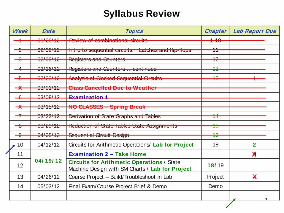
Syllabus Review
Week Date Topics Chapter Lab Report Due
1 01/26/12 Review of combinational circuits 1-10
2 02/02/12 Intro to sequential circuits. Latches and flip-flops 11
3 02/09/12 Registers and Counters 12
4 02/16/12 Registers and Counters … continued 12
5 02/23/12 Analysis of Clocked Sequential Circuits 13 1
X 03/01/12 Class Cancelled Due to Weather
6 03/08/12 Examination 1
X 03/15/12 NO CLASSES – Spring Break
7 03/22/12 Derivation of State Graphs and Tables 14
8 03/29/12 Reduction of State Tables State Assignments 15
9 04/05/12 Sequential Circuit Design 16
10 04/12/12 Circuits for Arithmetic Operations/ Lab for Project 18 2
1104/19/12
Examination 2 – Take Home 3
12 Circuits for Arithmetic Operations / State Machine Design with SM Charts / Lab for Project 18/19
13 04/26/12 Course Project – Build/Troubleshoot in Lab Project 4
14 05/03/12 Final Exam/Course Project Brief & Demo Demo
X
X

Course Project
• Guidelines are on the Class Web Page
• Any questions???
6

7
Questions?

8
Chapter 18 …
Circuits for Arithmetic Operations

9
Objectives
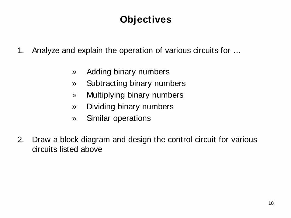
Objectives
1. Analyze and explain the operation of various circuits for …
» Adding binary numbers » Subtracting binary numbers » Multiplying binary numbers » Dividing binary numbers» Similar operations
2. Draw a block diagram and design the control circuit for various circuits listed above
10

Overview
• Using a sequential circuit to control a sequence of operations in a digital system
– Such a control circuit outputs a sequence of control signals that cause operations such as addition or shifting to take place at the appropriate times
11

12
Serial Adder with Accumulator

Serial Adder with Accumulator
• Design a control circuit for a serial adder with an accumulator
13
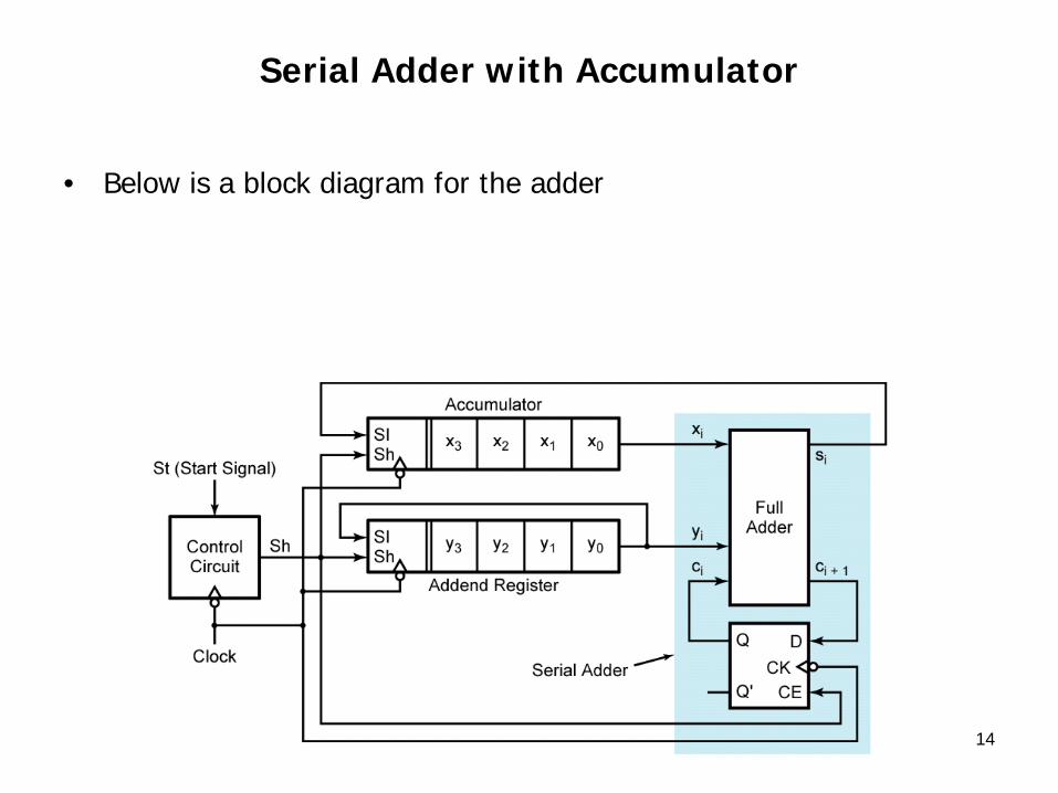
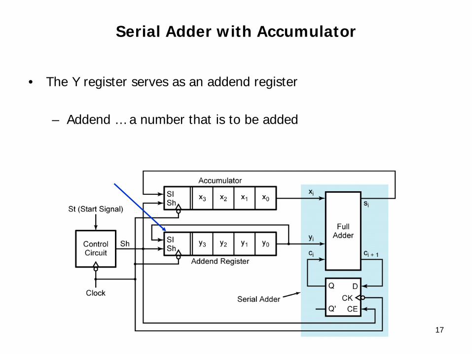
Serial Adder with Accumulator
• Below is a block diagram for the adder
14

Serial Adder with Accumulator
• Two shift registers are used to hold the 4-bit numbers to be added … X … and … Y
15

Serial Adder with Accumulator
• The X register serves as an accumulator
– Accumulator … processor register for storing intermediate results
16
Serial Adder with Accumulator
• The Y register serves as an addend register
– Addend … a number that is to be added
17
Serial Adder with Accumulator
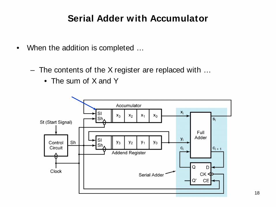
• When the addition is completed …
– The contents of the X register are replaced with …• The sum of X and Y
18

Serial Adder with Accumulator
• The addend register is connected as a cyclic shift register so that after shifting four times it is back in its original state
– The number Y is not lost
19

Serial Adder with Accumulator
• Inputs …– Sh … shift signal– SI … serial input– Clock
20

Serial Adder with Accumulator
• When Sh = 1 and an active clock edge occurs …– SI is entered into x3 … or … y3 at the same time as the contents
of the register are shifted one place to the right
21

Serial Adder with Accumulator
• The serial adder … in blue …– The full adder is a combinational circuit
22

Serial Adder with Accumulator
• At each clock … one pair of bits is added
• Because the full adder is a combinational circuit … the sum and carry appear at the Full Adder output after the propagation delay
23
Serial Adder with Accumulator
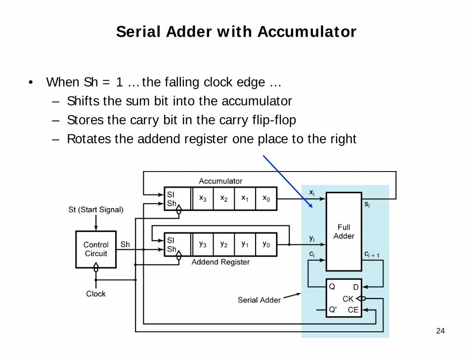
• When Sh = 1 … the falling clock edge …– Shifts the sum bit into the accumulator– Stores the carry bit in the carry flip-flop– Rotates the addend register one place to the right
24
Serial Adder with Accumulator
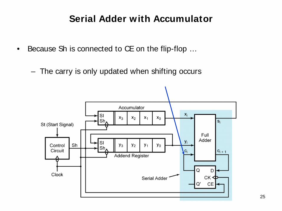
• Because Sh is connected to CE on the flip-flop …
– The carry is only updated when shifting occurs
25

26
Operation of the Adder

Serial Adder with Accumulator
• Operation of the adder …
27

Serial Adder with Accumulator
• Shifting occurs on the falling clock edge when Sh = 1
28

Serial Adder with Accumulator
• At t0 … which is the time before the first shift … the accumulator contains X and the addend register contains Y
• Because the full adder is a combinational circuit … x0 … y0 ... and … c0 are added independently of the clock to form the sum s0 and carry c1
29

Serial Adder with Accumulator
• When the first falling clock edge occurs …– s0 is shifted into the accumulator – The remaining accumulator digits are shifted one position to the
right– The same clock edge stores c1 in the carry flip-flop and rotates
the addend register right
30
Serial Adder with Accumulator
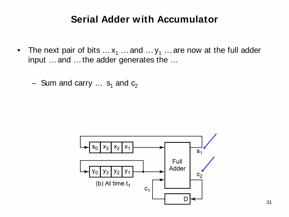
• The next pair of bits … x1 … and … y1 … are now at the full adder input … and … the adder generates the …
– Sum and carry … s1 and c2
31
Serial Adder with Accumulator
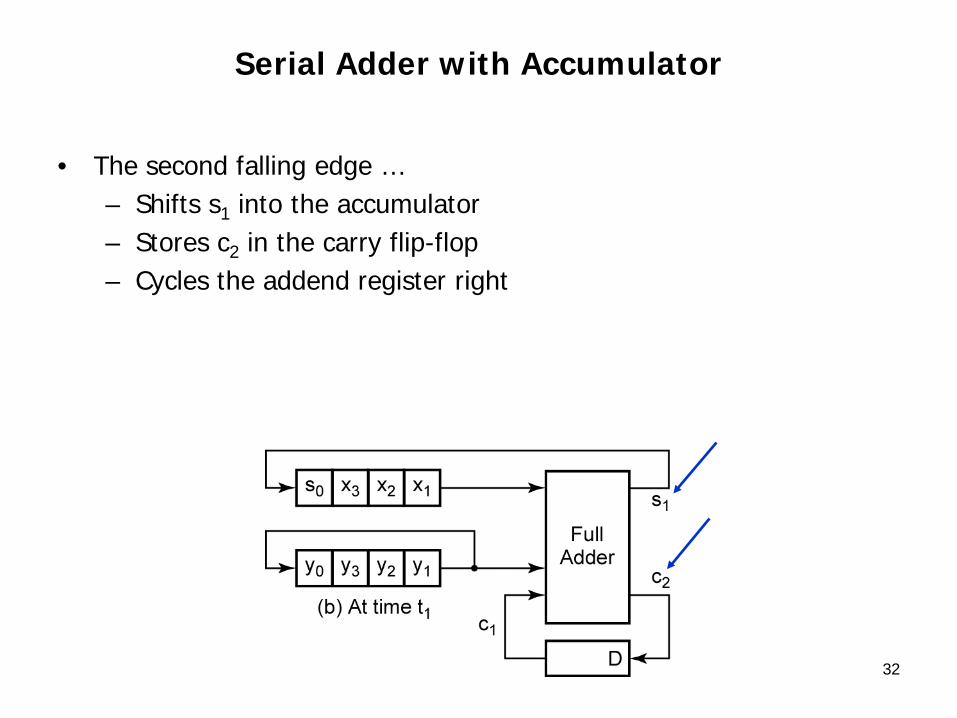
• The second falling edge …– Shifts s1 into the accumulator– Stores c2 in the carry flip-flop– Cycles the addend register right
32

Serial Adder with Accumulator
• Bits x2 and y2 are now at the adder input …
33

Serial Adder with Accumulator
• The process continues until all bit pairs have been added …
34

35
Example …
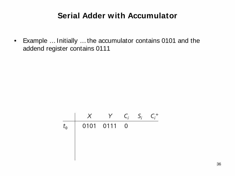
Serial Adder with Accumulator
• Example … Initially … the accumulator contains 0101 and the addend register contains 0111
36
Serial Adder with Accumulator
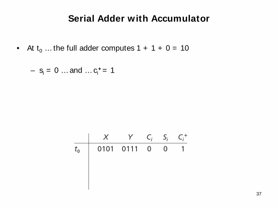
• At t0 … the full adder computes 1 + 1 + 0 = 10
– si = 0 … and … ci+= 1
37

Serial Adder with Accumulator
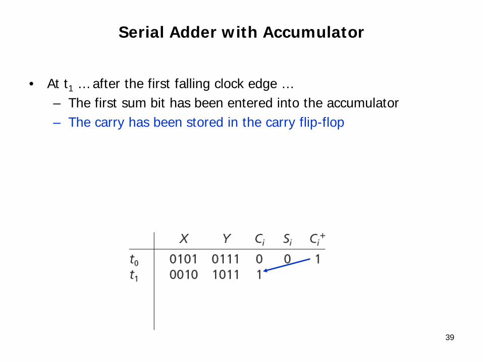
• At t1 … after the first falling clock edge … – The first sum bit has been entered into the accumulator
38
Serial Adder with Accumulator
• At t1 … after the first falling clock edge … – The first sum bit has been entered into the accumulator – The carry has been stored in the carry flip-flop
39
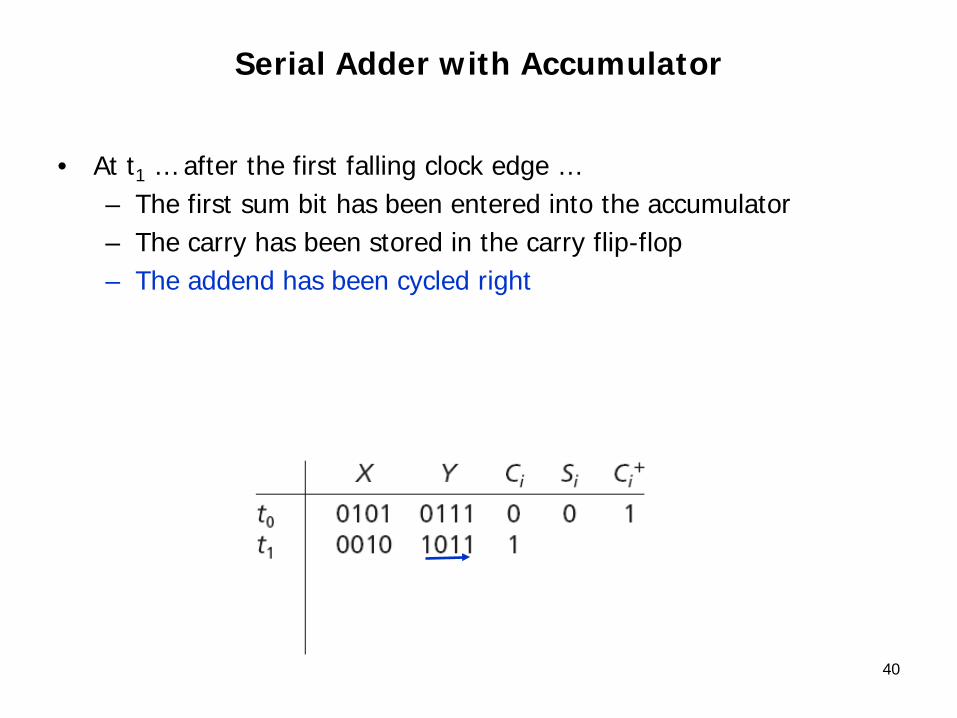
Serial Adder with Accumulator
• At t1 … after the first falling clock edge … – The first sum bit has been entered into the accumulator – The carry has been stored in the carry flip-flop– The addend has been cycled right
40
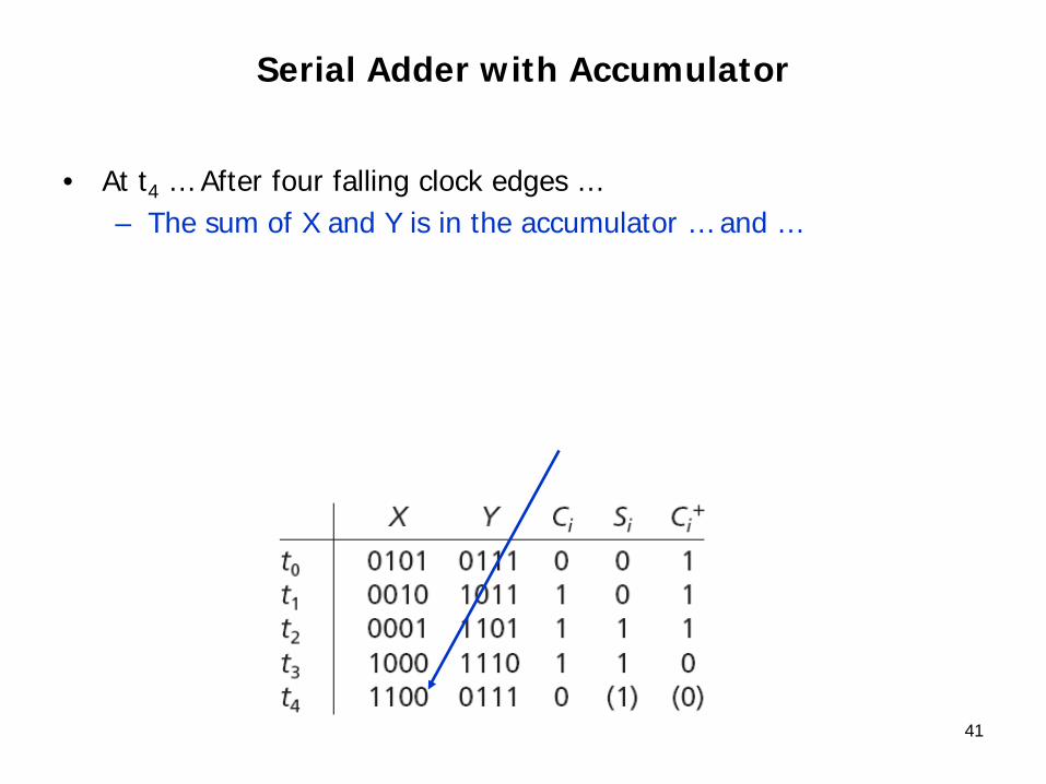
Serial Adder with Accumulator
• At t4 … After four falling clock edges …– The sum of X and Y is in the accumulator … and …
41

Serial Adder with Accumulator
• At t4 … After four falling clock edges …– The sum of X and Y is in the accumulator … and …– The addend register is back to its original state
42

43
Adder Control Circuit …

Adder Control Circuit
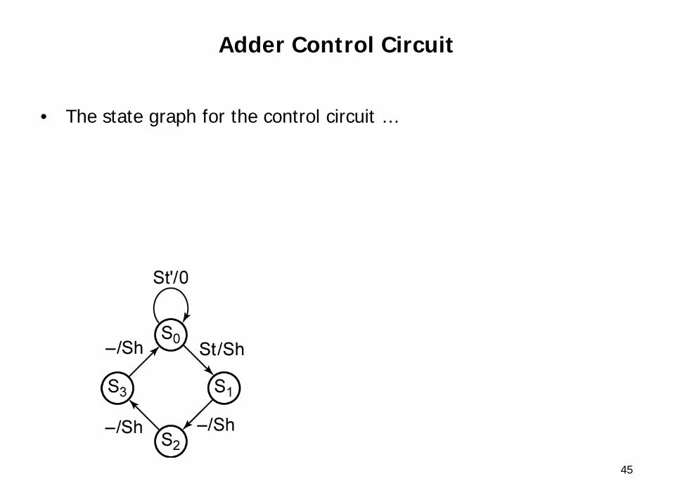
• Design the control circuit for the adder …
– After receiving a start signal …
• The control circuit will put out four shift signals and then stop
44
Adder Control Circuit
• The state graph for the control circuit …
45

Adder Control Circuit
• The circuit remains in S0 until a start signal is received … at which time the circuit outputs Sh = 1 and goes to S1
46

Adder Control Circuit
• Then … at successive clock times … three more shift signals are put out
– It will be assumed that the start signal is terminated before the circuit returns to state S0 so that no further output occurs until another start signal is received
47

Adder Control Circuit
• Dashes appear on the graph because once S1 is reached … the circuit operation continues regardless of the value of St
48

Adder Control Circuit
• State table is developed …
49
Next State Sh St = 0 1 0 1
S0 S0 S1 0 1 S1 S2 S2 1 1 S2 S3 S3 1 1 S3 S0 S0 1 1

Adder Control Circuit
• Starting with the state table … and using a straight binary state assignment … the control circuit equations are derived
50
Next State Sh St = 0 1 0 1
S0 S0 S1 0 1 S1 S2 S2 1 1 S2 S3 S3 1 1 S3 S0 S0 1 1
AB A+B+ 0 1
S0 00 00 01 S1 01 10 10 S2 10 11 11 S3 11 00 00

51
Typical Serial Processing Unit …
Typical Serial Processing Unit
• A serial processing unit …
– Such as a serial adder with an accumulator …
• Processes data one bit at a time
52

Typical Serial Processing Unit
• Shown below is a typical serial processing unit – It has two shift registers
53

Typical Serial Processing Unit
• Shown below is a typical serial processing unit – It has two shift registers– The output bits from the shift register are inputs to a
combinational circuit
54

Typical Serial Processing Unit
• Shown below is a typical serial processing unit – It has two shift registers– The output bits from the shift register are inputs to a
combinational circuit• The combinational circuit generates at least one output bit
55

Typical Serial Processing Unit
• Shown below is a typical serial processing unit – It has two shift registers– The output bits from the shift register are inputs to a
combinational circuit• The combinational circuit generates at least one output bit
– This output bit is fed into the input of a shift register
56

Typical Serial Processing Unit
• Shown below is a typical serial processing unit – It has two shift registers– The output bits from the shift register are inputs to a
combinational circuit• The combinational circuit generates at least one output bit
– This output bit is fed into the input of a shift register– When the active clock edge occurs … this bit is stored in
the first bit of the shift register at the same time the register bits are shifted to the right
57

Typical Serial Processing Unit
• The control for the serial processing unit generates a series of shift signals
58

Typical Serial Processing Unit
• When the start signal … St … is … 1 … the first shift signal .. Sh … is generated
59

Typical Serial Processing Unit
• If the shift registers have n bits … then a total of n shift signals must be generated
60

Typical Serial Processing Unit
• If St is 1 for only one clock time … then the control state graph stops when it returns to state S0
61
Typical Serial Processing Unit
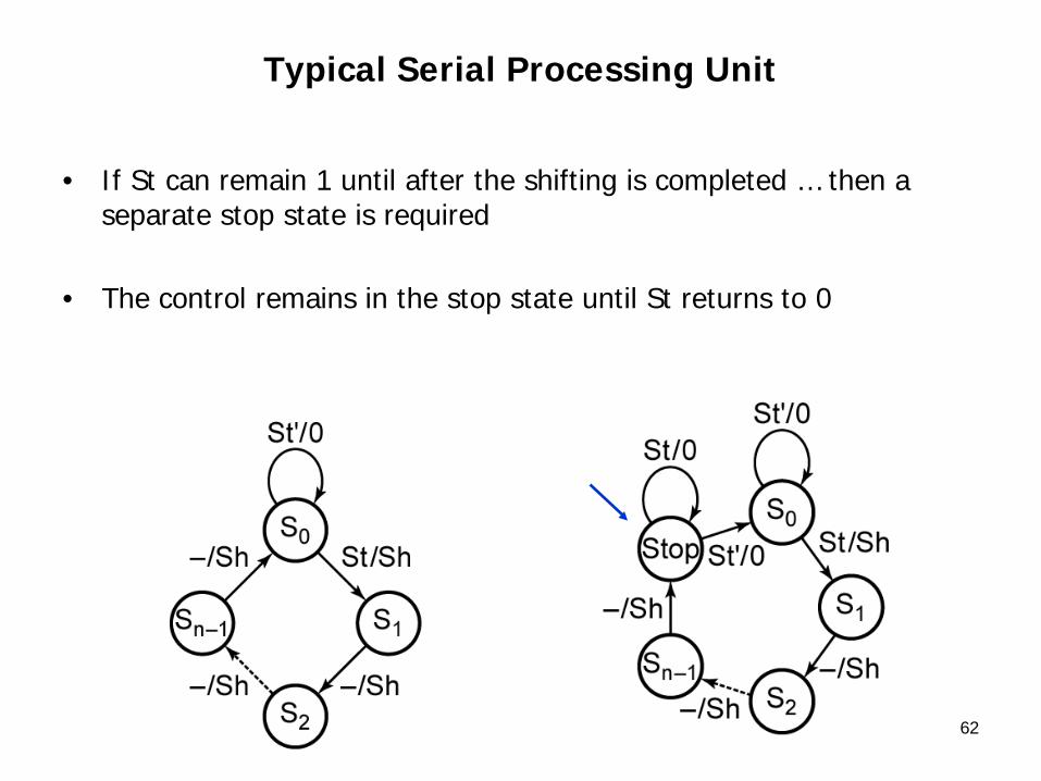
• If St can remain 1 until after the shifting is completed … then a separate stop state is required
• The control remains in the stop state until St returns to 0
62

63
Design of a Parallel Multiplier

Design of a Parallel Multiplier
• Design a parallel multiplier for positive binary numbers
• Binary multiplication requires only shifting and adding – Each partial product is added in as soon as it is formed– This eliminates the need for adding more than two binary
numbers at a time
64

Design of a Parallel Multiplier
• The multiplication of two 4-bit numbers requires … – A 4-bit multiplicand register– A 4-bit multiplier register– 8-bit register for the product
• The product register serves as an accumulator to accumulate the sum of the partial products
• Instead of shifting the multiplicand left each time before it is added … – It is more convenient to shift the product register to the right
each time
65

Design of a Parallel Multiplier
• Below shows a block diagram for Parallel Binary Multiplier
66

Design of a Parallel Multiplier
• As indicated by the arrows on the diagram … – 4 bits from the accumulator … and … – 4 bits from the multiplicand register are connected to the adder
inputs
67

Design of a Parallel Multiplier
• The 4 sum bits … and … the carry output from the adder are connected back to the accumulator
68

Design of a Parallel Multiplier
• The adder calculates the sum of its inputs … and … – When an add signal … Ad … occurs … the adder outputs are
stored in the accumulator by the next rising clock edge … thus causing the multiplicand to be added to the accumulator
69
Design of a Parallel Multiplier
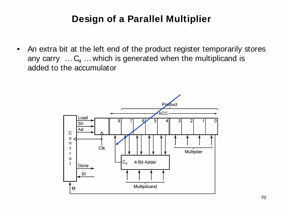
• An extra bit at the left end of the product register temporarily stores any carry … C4 … which is generated when the multiplicand is added to the accumulator
70

Design of a Parallel Multiplier
• Because the lower four bits of the product register are initially unused … we will store the multiplier in this location instead of in a separate register
• As each multiplier bit is used … it is shifted out the right end of the register to make room for additional product bits
71

Design of a Parallel Multiplier
• The Load signal …– Loads the multiplier into the lower four bits of ACC … and …– At the same time clears the upper 5 bits
72

Design of a Parallel Multiplier
• The shift signal … Sh… causes the …– Contents of the product register … including the multiplier … to
be shifted one place to the right when the next rising clock edge occurs
73

Design of a Parallel Multiplier
• The control circuit puts out the proper sequence of add and shift signals after a start signal … St = 1 … has been received
74

Design of a Parallel Multiplier
• The control circuit puts out the proper sequence of add and shift signals after a start signal … St = 1 … has been received– If the current multiplier bit … M … is 1 … the multiplicand is
added to the accumulator followed by a right shift
75

Design of a Parallel Multiplier
• The control circuit puts out the proper sequence of add and shift signals after a start signal … St = 1 … has been received– If the multiplier bit is … 0 … the addition is skipped and only the
right shift occurs
76

77
Example …

Parallel Multiplier - Example
• Example … Multiply … 13 X 11
78

Parallel Multiplier - Example
• Example … Multiply … 13 X 11
Dividing line between product and multipler
79

Parallel Multiplier - Example
• Example … Multiply … 13 X 11 … continued
80
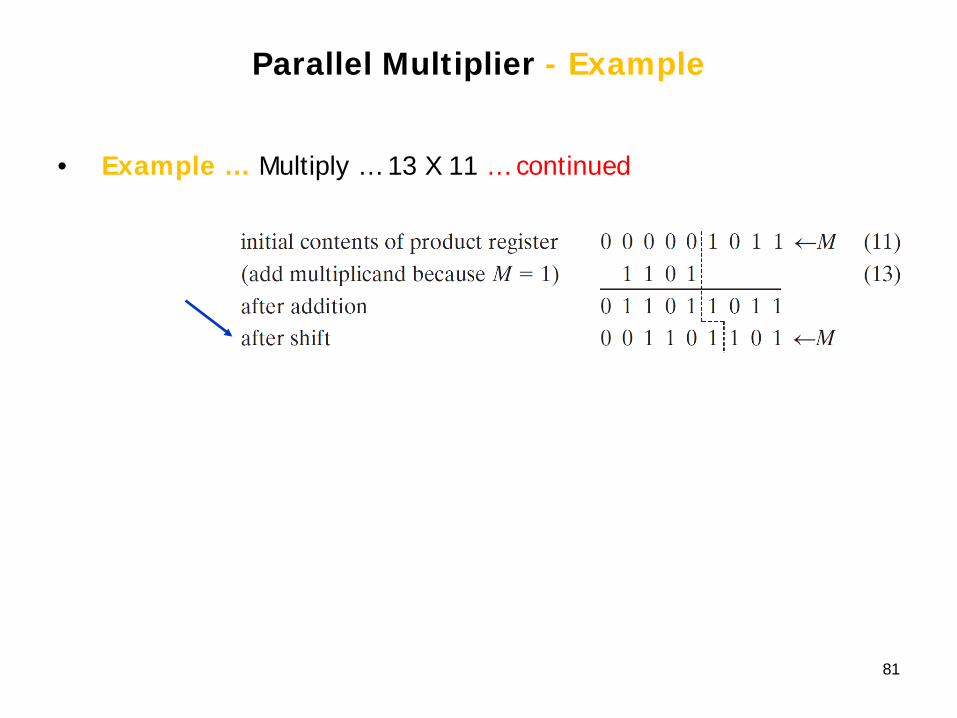
Parallel Multiplier - Example
• Example … Multiply … 13 X 11 … continued
81

Parallel Multiplier - Example
• Example … Multiply … 13 X 11 … continued
82

Parallel Multiplier - Example
• Example … Multiply … 13 X 11 … continued
83

Parallel Multiplier - Example
• Example … Multiply … 13 X 11 … continued
84

Parallel Multiplier - Example
• Example … Multiply … 13 X 11 … continued
85

Parallel Multiplier - Example
• Example … Multiply … 13 X 11 … continued
86

87
Multiplier Control Circuit …

• The control circuit must be designed to output the proper sequence of add and shift signals
• Below shows a state graph for the control circuit
Multiplier Control Circuit
88

• M/Ad means … if M = 1 … then the output Ad is 1 … and the other outputs are 0
Multiplier Control Circuit
89

• M’/Sh means … if M' = 1 … M = 0 … then … the output Sh is 1 … and the other outputs are 0
Multiplier Control Circuit
90

• S0 is the reset state … and the circuit stays in S0 until a start signal … St = 1 … is received
Multiplier Control Circuit
91

• St = 1 … generates a Load signal … which causes – The multiplier to be loaded into the lower 4 bits of the
accumulator (ACC) … and the …– Upper 5 bits of ACC to be cleared on the next rising clock edge
Multiplier Control Circuit
92

• In state S1 … the low order bit of the multiplier … M … is tested– If M = 1 …
• An add signal is generated and, then, a shift signal is generated in S2
Multiplier Control Circuit
93

• In state S1 … the low order bit of the multiplier … M … is tested– If M = 1 …
• If M = 0 in S1 … a shift signal is generated because adding 0 can be omitted
Multiplier Control Circuit
94

• M is tested in the other states to determine whether to generate an add signal followed by shift or just a shift signal
Multiplier Control Circuit
95

• After four shifts have been generated …– All four multiplier bits have been processed and the control
circuit goes to a Done state and terminates the multiplication process
Multiplier Control Circuit
96

97
Multiplier Using a Counter …

Multiplier Using a Counter
• As the previous state graph indicated … the control performs two functions … – Generating add or shift signals as needed … and … – Counting the number of shifts
• If the number of bits is large … it is convenient to divide the control circuit into a counter and an add-shift control
98

Multiplier Using a Counter
• Below shows a counter and an add-shift control block diagram …
99

Multiplier Using a Counter
• We derived a state graph for the add-shift control which tests M and St … and … outputs the proper sequence of add and shift signals
100

Multiplier Using a Counter
• We added a completion signal … K … from the counter which stops the multiplier after the proper number of shifts have been completed
101

Multiplier Using a Counter
• The state graph generates the proper sequence of add and shift signals … but it has no provision for stopping the multiplier
102

Multiplier Using a Counter
• If the multiplier is n bits … a total of n shifts are required• Design the counter so that a completion signal … K … is generated
after n - 1 shifts have occurred• The last shift signal will reset the counter to 0 at the same time the
add-shift control goes to the Done state
103

104
Example …

Multiplier Using a Counter - Example
• Example … Replace the control circuit with the multiplier control circuit. Then again … Multiply … 13 X 11.
105

Multiplier Using a Counter - Example
• Example … Replace the control circuit with the multiplier control circuit. Then again … Multiply … 13 X 11.– Because n = 4 … a 2-bit counter is needed … and K = 1 when
the counter is in state 3 (112)
106
Parallel Multiplier - Example
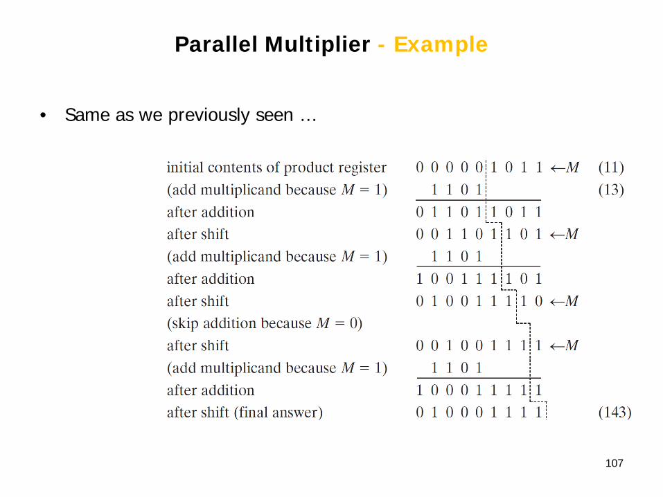
• Same as we previously seen …
107

Multiplier Using a Counter - Example
• At time t0 … the control is reset and waiting for a start signal
108
Time State Counter Product Register
St M K Load Ad Sh Done
t0 S0 00 000000000 0 0 0 0 0 0 0 t1 S0 00 000000000 1 0 0 1 0 0 0 t2 S1 00 000001011 0 1 0 0 1 0 0 t3 S2 00 011011011 0 1 0 0 0 1 0 t4 S1 01 001101101 0 1 0 0 1 0 0 t5 S2 01 100111101 0 1 0 0 0 1 0 t6 S1 10 010011110 0 0 0 0 0 1 0 t7 S1 11 001001111 0 1 1 0 1 0 0 t8 S2 11 100011111 0 1 1 0 0 1 0 t9 S3 00 010001111 0 1 0 0 0 0 1

Multiplier Using a Counter - Example
• At time t1 … the start signal St = 1 … and … a Load signal is generated
109
Time State Counter Product Register
St M K Load Ad Sh Done
t0 S0 00 000000000 0 0 0 0 0 0 0 t1 S0 00 000000000 1 0 0 1 0 0 0 t2 S1 00 000001011 0 1 0 0 1 0 0 t3 S2 00 011011011 0 1 0 0 0 1 0 t4 S1 01 001101101 0 1 0 0 1 0 0 t5 S2 01 100111101 0 1 0 0 0 1 0 t6 S1 10 010011110 0 0 0 0 0 1 0 t7 S1 11 001001111 0 1 1 0 1 0 0 t8 S2 11 100011111 0 1 1 0 0 1 0 t9 S3 00 010001111 0 1 0 0 0 0 1

Multiplier Using a Counter - Example
• At time t2 … M = 1 so an Ad signal is generated• When the next clock occurs … the output of the adder is loaded into
the accumulator and the control goes to S2
110
Time State Counter Product Register
St M K Load Ad Sh Done
t0 S0 00 000000000 0 0 0 0 0 0 0 t1 S0 00 000000000 1 0 0 1 0 0 0 t2 S1 00 000001011 0 1 0 0 1 0 0 t3 S2 00 011011011 0 1 0 0 0 1 0 t4 S1 01 001101101 0 1 0 0 1 0 0 t5 S2 01 100111101 0 1 0 0 0 1 0 t6 S1 10 010011110 0 0 0 0 0 1 0 t7 S1 11 001001111 0 1 1 0 1 0 0 t8 S2 11 100011111 0 1 1 0 0 1 0 t9 S3 00 010001111 0 1 0 0 0 0 1

Multiplier Using a Counter - Example
• At t3 … an Sh signal is generated … so … shifting occurs and the counter is incremented at the next clock
111
Time State Counter Product Register
St M K Load Ad Sh Done
t0 S0 00 000000000 0 0 0 0 0 0 0 t1 S0 00 000000000 1 0 0 1 0 0 0 t2 S1 00 000001011 0 1 0 0 1 0 0 t3 S2 00 011011011 0 1 0 0 0 1 0 t4 S1 01 001101101 0 1 0 0 1 0 0 t5 S2 01 100111101 0 1 0 0 0 1 0 t6 S1 10 010011110 0 0 0 0 0 1 0 t7 S1 11 001001111 0 1 1 0 1 0 0 t8 S2 11 100011111 0 1 1 0 0 1 0 t9 S3 00 010001111 0 1 0 0 0 0 1

Multiplier Using a Counter - Example
• At t4 … M = 1 … so … Ad= 1 … and the adder output is loaded into the accumulator at the next clock
112
Time State Counter Product Register
St M K Load Ad Sh Done
t0 S0 00 000000000 0 0 0 0 0 0 0 t1 S0 00 000000000 1 0 0 1 0 0 0 t2 S1 00 000001011 0 1 0 0 1 0 0 t3 S2 00 011011011 0 1 0 0 0 1 0 t4 S1 01 001101101 0 1 0 0 1 0 0 t5 S2 01 100111101 0 1 0 0 0 1 0 t6 S1 10 010011110 0 0 0 0 0 1 0 t7 S1 11 001001111 0 1 1 0 1 0 0 t8 S2 11 100011111 0 1 1 0 0 1 0 t9 S3 00 010001111 0 1 0 0 0 0 1

Multiplier Using a Counter - Example
• At t5 and t6 … shifting and counting occurs
113
Time State Counter Product Register
St M K Load Ad Sh Done
t0 S0 00 000000000 0 0 0 0 0 0 0 t1 S0 00 000000000 1 0 0 1 0 0 0 t2 S1 00 000001011 0 1 0 0 1 0 0 t3 S2 00 011011011 0 1 0 0 0 1 0 t4 S1 01 001101101 0 1 0 0 1 0 0 t5 S2 01 100111101 0 1 0 0 0 1 0 t6 S1 10 010011110 0 0 0 0 0 1 0 t7 S1 11 001001111 0 1 1 0 1 0 0 t8 S2 11 100011111 0 1 1 0 0 1 0 t9 S3 00 010001111 0 1 0 0 0 0 1

Multiplier Using a Counter - Example
• At t7 three shifts have occurred and the counter state is 11 … so … K = 1
• Because M = 1 … addition occurs and the control goes to S2
114
Time State Counter Product Register
St M K Load Ad Sh Done
t0 S0 00 000000000 0 0 0 0 0 0 0 t1 S0 00 000000000 1 0 0 1 0 0 0 t2 S1 00 000001011 0 1 0 0 1 0 0 t3 S2 00 011011011 0 1 0 0 0 1 0 t4 S1 01 001101101 0 1 0 0 1 0 0 t5 S2 01 100111101 0 1 0 0 0 1 0 t6 S1 10 010011110 0 0 0 0 0 1 0 t7 S1 11 001001111 0 1 1 0 1 0 0 t8 S2 11 100011111 0 1 1 0 0 1 0 t9 S3 00 010001111 0 1 0 0 0 0 1

Multiplier Using a Counter - Example
• At t8 … Sh = K = 1 … so … at the next clock the final shift occurs … and the counter is incremented back to state 00
115
Time State Counter Product Register
St M K Load Ad Sh Done
t0 S0 00 000000000 0 0 0 0 0 0 0 t1 S0 00 000000000 1 0 0 1 0 0 0 t2 S1 00 000001011 0 1 0 0 1 0 0 t3 S2 00 011011011 0 1 0 0 0 1 0 t4 S1 01 001101101 0 1 0 0 1 0 0 t5 S2 01 100111101 0 1 0 0 0 1 0 t6 S1 10 010011110 0 0 0 0 0 1 0 t7 S1 11 001001111 0 1 1 0 1 0 0 t8 S2 11 100011111 0 1 1 0 0 1 0 t9 S3 00 010001111 0 1 0 0 0 0 1

Multiplier Using a Counter - Example
• At t9 … a Done signal is generated
116
Time State Counter Product Register
St M K Load Ad Sh Done
t0 S0 00 000000000 0 0 0 0 0 0 0 t1 S0 00 000000000 1 0 0 1 0 0 0 t2 S1 00 000001011 0 1 0 0 1 0 0 t3 S2 00 011011011 0 1 0 0 0 1 0 t4 S1 01 001101101 0 1 0 0 1 0 0 t5 S2 01 100111101 0 1 0 0 0 1 0 t6 S1 10 010011110 0 0 0 0 0 1 0 t7 S1 11 001001111 0 1 1 0 1 0 0 t8 S2 11 100011111 0 1 1 0 0 1 0 t9 S3 00 010001111 0 1 0 0 0 0 1

183
Lab

184
LABS
• Lab #2 is on the Class Web Page
– Due TONIGHT … April 12th
• Lab time … work on course projects

185
Next Week …

186
Next Week Topics
• Finish … Chapter 18 … Circuits for Arithmetic Operations
• Pages 594 – 607
• Start … Chapter 19 … State Machine Design with SM Charts
• Pages 623 – 640

187
Home Work

188
Homework
1. Read …
– Chapter 18 … Circuits for Arithmetic Operations– Pages 594 – 607
– Chapter 19 … State Machine Design with SM Charts– Pages 623 – 640
2. Chapter 18 … Programmed Exercises
3. Work on projects