LOGIC-CONTROLLED SOLID-STATE SWITCHGEAR · High voltage dc electric power systems ... The concept...
29
N74 13895 NASA TECHNICAL NASA TM X-71483 MEMORANDUM r- (NASA-TM X-71483) LOGIC-CONTROLLED SOLID N74- 1389 STATE SWITCHGEAR FOR 270 =VOLTS dc (NASA) 29 p HC CSCL 09E - Unclas G3/ 9 25681 z LOGIC-CONTROLLED SOLID-STATE SWITCHGEAR FOR 270 VOLTS DC by G. R. Sundberg 4 Lewis Research Center Cleveland, Ohio , and D. Waddington and E. E. Buchanan Jr. Martin Marietta Corporation Denver, Colorado TECHNICAL PAPER presented at Power Electronics Specialists Conference sponsored by the Institute of Electrical and Electronics Engineers Pasadena, California, June 11-13, 1973 REPRODUCED BY NATIONAL TECHNICAL INFORMATION SERVICE U.S. DEPARTMENT OF COMMERCE SPRINGFIELD. VA. 22161 https://ntrs.nasa.gov/search.jsp?R=19740005782 2018-06-18T10:37:30+00:00Z
Transcript of LOGIC-CONTROLLED SOLID-STATE SWITCHGEAR · High voltage dc electric power systems ... The concept...

N74 13895
NASA TECHNICAL NASA TM X-71483MEMORANDUM
r- (NASA-TM X-71483) LOGIC-CONTROLLED SOLID N74- 1389STATE SWITCHGEAR FOR 270 =VOLTS dc (NASA)29 p HC CSCL 09E
- UnclasG3/ 9 25681
z
LOGIC-CONTROLLED SOLID-STATE SWITCHGEAR
FOR 270 VOLTS DC
by G. R. Sundberg 4Lewis Research Center
Cleveland, Ohio ,
and
D. Waddington and E. E. Buchanan Jr.
Martin Marietta Corporation
Denver, Colorado
TECHNICAL PAPER presented at
Power Electronics Specialists Conference sponsored by
the Institute of Electrical and Electronics Engineers
Pasadena, California, June 11-13, 1973
REPRODUCED BYNATIONAL TECHNICALINFORMATION SERVICE
U.S. DEPARTMENT OF COMMERCESPRINGFIELD. VA. 22161
https://ntrs.nasa.gov/search.jsp?R=19740005782 2018-06-18T10:37:30+00:00Z
LOGIC-CONTROLLED SOLID-STATE SWITCHGEAR FOR
270 VOLTS DC*
by G. R. Sundherg, D. Waddington, ** and E. E. Buchanan Jr. **
Lewis Research Center
Cleveland, Ohio
SUMMARY
This report describes the results of a feasibility study to design and
demonstrate solid-state switchgear in the form of circuit breakers and a
power transfer switch. The switchgear operates on a nominal 270 V dc
circuit and controls power to a load of up to 15 amperes, One circuit
breaker may be interconnected to a second breaker to form a power
transfer switch. On-off and transfer functions of the breakers or the
transfer switch are remotely controlled. A number of reclosures with
variable time delay between tripout and reclosure are programmed and
controlled by integrated analog and COSMOS logic circuits. A unique
commutation circuit, that generates only minimal transient disturbance
to either source or load, was developed to interrupt current flow through
the main SCR switching element. Laboratory tests demonstrated perfor-
mance of the solid-state circuit breakers over specified voltage and temp-
erature ranges.
This work was supported by the NASA- Lewis Research Center under
Contract NAS3-15824.**
Electronics Research, Martin Marietta Corporation, Denver,Color ado
/,

2
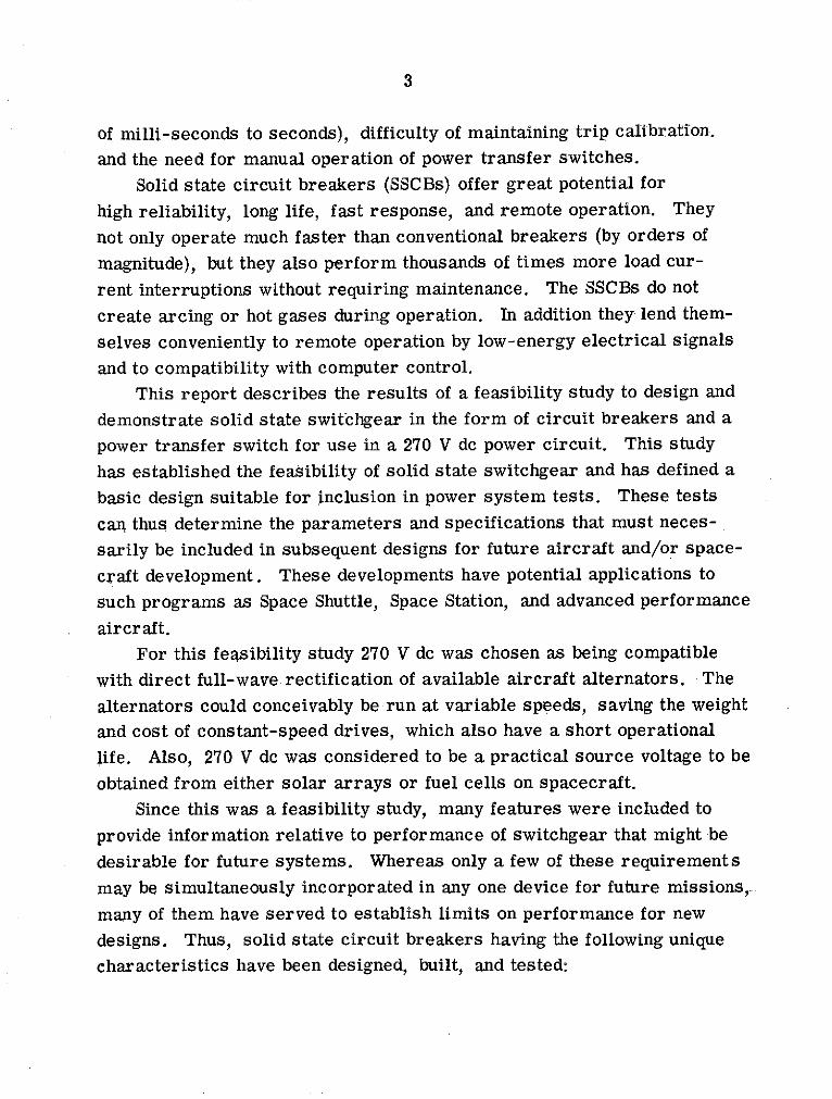
BACKGROUND
High voltage dc electric power systems (above 100 V dc) are seri-
ously being considered as candidate systems for future generation air
and spacecraft. Recent NASA sponsored studies and investigations by
DOD agencies show that high voltage de transmission and distribution
can provide significant weight reduction, greater design flexibility,higher reliability, and lower cost than conventional 28 V dc or 115 V ac
systems. The optimum dc system voltage appears to be about 300 V dc
when all factors are considered including corona breakdown. System
voltages ranging from 120 to 300 V dc are being recommended as
having maximum advantages, in general, and therefore are the most
desirable for future development.Several significant technology problem areas that impede the ap-*.
plication of these high voltage concepts to electric power systems have
been identified. One of the principal problem areas is the need for
demonstrated, space rated, power control and protection devices for
power electronic circuits and systems. Optimum system concepts may
require automatic power management using advanced concepts of remote
control, status reporting, and display as obtained by coupling computer
multiplexing techniques, with the remote control concept. This approach
will provide faster reaction times while minimizing transmission and
distribution wire lengths. In addition it should provide increased reli-
ability and flexibility for system supervision, reconfiguration and check-
put.The continued and increasing complexity of modern aircraft and
spacecraft places greater demands on the performance of electric power
circuitry. These demands require consideration of much more rapid
fault sensing and reaction to protect electrical and electronic equip-
ment. Circuit breakers should protect both the power transmission
cables and associated loads, circuits, and components, which are a
part of the power system. Currently available electromechanical switch-
gear suffer from limited reliability and from functional limitations.
Their high failure probability due to contact erosion limits reliability.The functional limitations include relatively slow response times (the order
3
of milli-seconds to seconds), difficulty of maintaining trip calibration.
and the need for manual operation of power transfer switches.
Solid state circuit breakers (SSCBs) offer great potential for
high reliability, long life, fast response, and remote operation. They
not only operate much faster than conventional breakers (by orders of
magnitude), but they also perform thousands of times more load cur-
rent interruptions without requiring maintenance. The SSCBs do not
create arcing or hot gases during operation. In addition they lend them-
selves conveniently to remote operation by low-energy electrical signals
and to compatibility with computer control.
This report describes the results of a feasibility study to design and
demonstrate solid state switchgear in the form of circuit breakers and a
power transfer switch for use in a 270 V de power circuit. This study
has established the feasibility of solid state switchgear and has defined a
basic design suitable for inclusion in power system tests. These tests
can thus determine the parameters and specifications that must neces-
sarily be included in subsequent designs for future aircraft and/or space-
craft development. These developments have potential applications to
such programs as Space Shuttle, Space Station, and advanced performance
aircraft.
For this feasibility study 270 V dc was chosen as being compatible
with direct full-wave rectification of available aircraft alternators. The
alternators could conceivably be run at variable speeds, saving the weight
and cost of constant-speed drives, which also have a short operational
life. Also, 270 V dc was considered to be a practical source voltage to be
obtained from either solar arrays or fuel cells on spacecraft.
Since this was a feasibility study, many features were included to
provide information relative to performance of switchgear that might be
desirable for future systems. Whereas only a few of these requirements
may be simultaneously incorporated in any one device for future missions,
many of them have served to establish limits on performance for new
designs. Thus, solid state circuit breakers having the following unique
characteristics have been designed, built, and tested:

4
(1) Carry a continuous dc current up to 15 A in a supply line at
270 ±27 V dc;(2) Trip out at an adjustable current level of 18 to 45 A;
(3) React to transient overloads below the ultimate trip level on
an energy basis proportional to 12t within the limits
5<I2t<30;(4) Provide programmable 0 to 9 automatic resets with adjustable
delay times of 1. 5 to 100 ms between resets;
(5) Have a forward voltage drop of less than 3 V dc with a load
current of 15 A;(6) Provide operation from isolated low-energy remote control
signals of less than 1 millijoule;
(7) Perform all functions in the presence of transient overvoltages
up to 300 V above line voltage for a 10 /is duration;
(8) Operate over a temperature range of -45 to 1000 C;
(9) Provide isolation from susceptibility to malfunctions due to
extraneous voltages, currents, and EMI;
(10) Connect to form a power transfer switch operating in the "break
before make" mode.
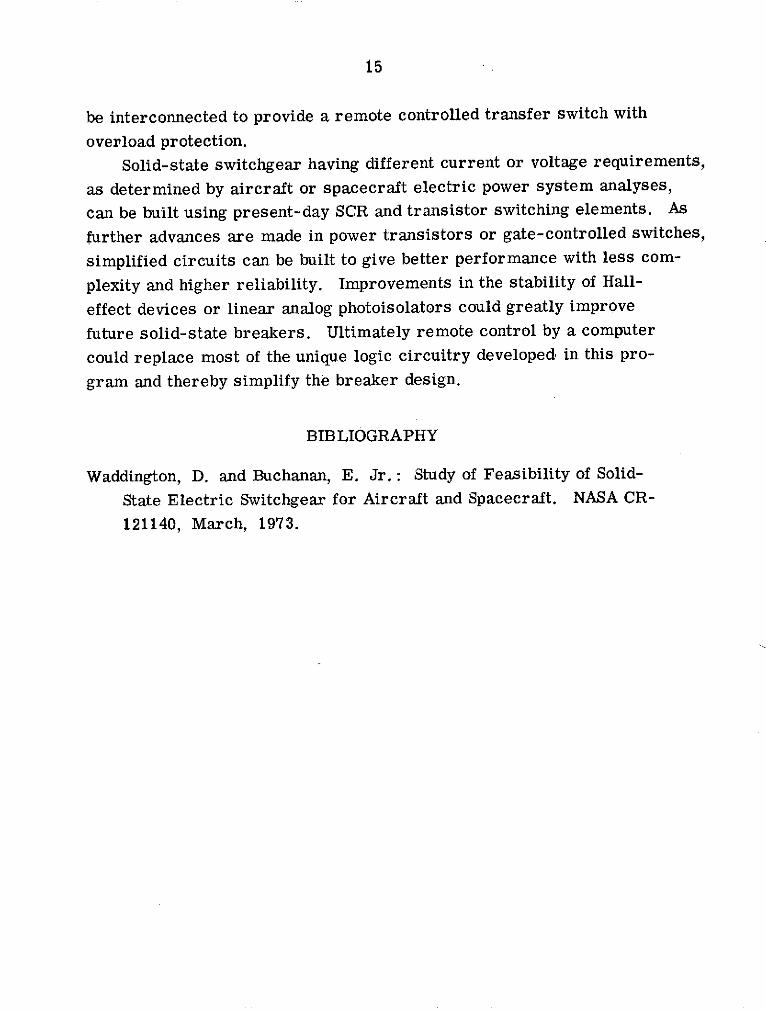
DESIGN CONCEPT
The concept of the logic-controlled solid-state circuit breaker is
illustrated by the block diagram shown in figure 1. The power
from the 270 V dc source is fed through the solid-state switching element
and then through a current sensor into the load. An analog circuit de-
termines whether the sensed current represents an overload. If an over-
load is sensed, the analog circuit then sends a trip signal to the power
switching circuit. A logic circuit provides on-off command functions and
isolation, together with all timing, reset, and recycle counting related to
automatic reclosure. An internal electronic power supply provides all the
internal operating voltages. Each of these functional blocks is discussedin the following paragraphs.

5
SWITCHING CIRCUIT
From a circuit design standpoint, it would be desirable to place the
power switching element in the return lead and to maintain this lead at
ground potential. However, since the circuit breaker was necessarily
general purpose, and since it was necessary to insure that the load
could be grounded by grounding the power return, the switching element
was placed in the +270 V dc line.
Due to the high voltage requirements (270±27 V) and the nominal cur-
rent of 15 A with overloads up to 45 A specified, the main solid state switch-
ing element was determined to be a silicon controlled retified (SCR). Sel-
ection of the main-switching SCR involved a number of requirements which
had to be considered collectively. High blocking voltages were an initial
requirement, because any conceivable switching operation involved transients
that could be several times the source voltage. Fast recovery devices were
essential to insure turn-off with a minimum of energy storage and/or loss.
SCRs with fast recovery were also required to comply with the one milli-
second recycle time.
In order to turn off an SCR, it is necessary to reduce the current
flowing through it to a low value (sub-holding current) or, more pref-
erably to a zero-current condition. This can be conventionally achieved
by applying a reverse potential for a time sufficiently long to allow the
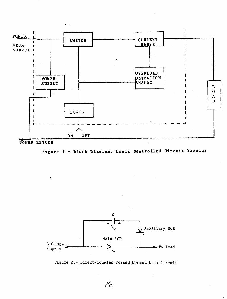
device to recover its blocking capability. The basic circuit for forced-
commutation is shown in figure 2.
Numerous approaches toward commutation were evaluated and dis-
carded for various reasons. The major problems were either that theenergy of commutation had to be dissipated through the load (the case
with the circuit shown in figure 2), or that voltages developed across the
SCR or the commutation capacitor during the commutation cycle wereexcessive. The basic commutation circuit eventually used in the circuit
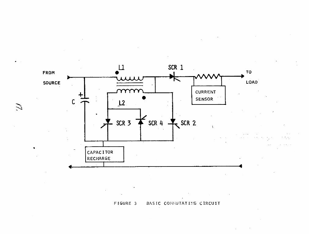
breaker is shown in figure 3.
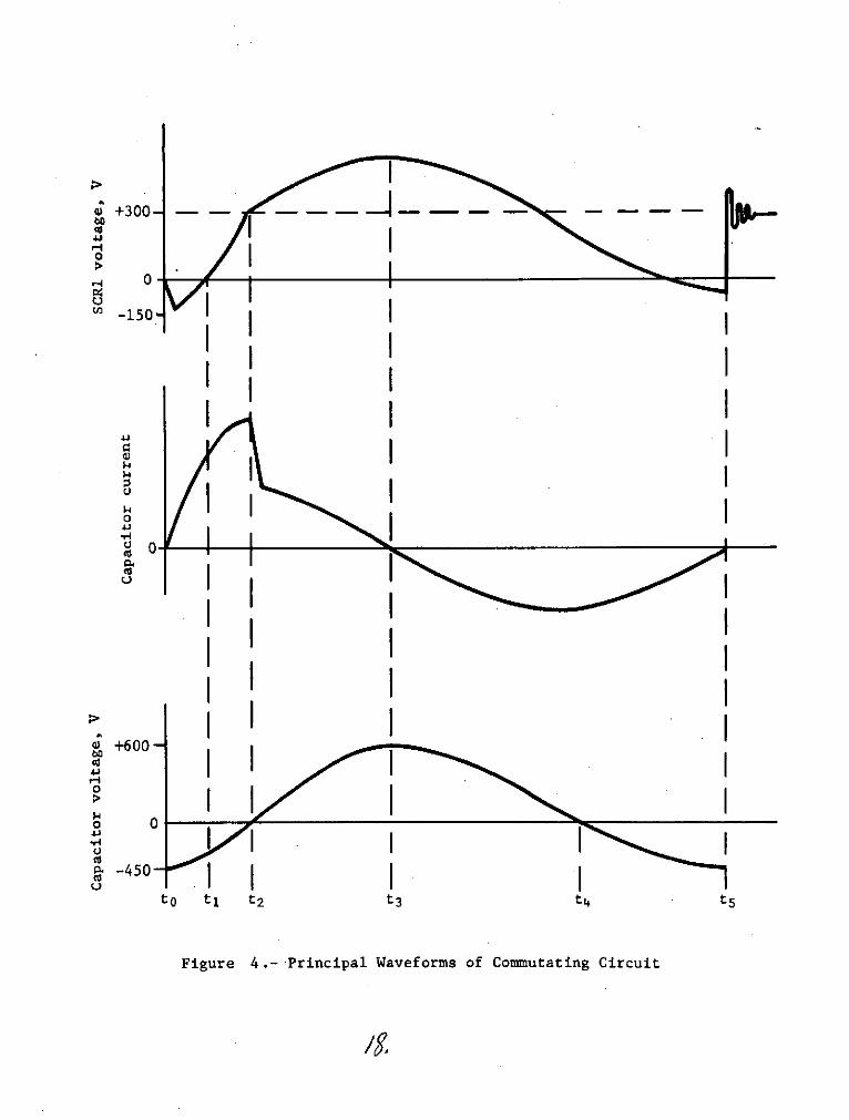
Assume that SCR-1 is gated on and carrying load current. The cap-acitor C1 is pre-charged to approximately 450 volts in the polarity indi-cated. Reference is now made to figure 4 to illustrate the operation ofthe commutation circuit.
6
In the event of an external turn-off command, or a sensed over-
current generated trip signal, SCR-2 is gated on. This occurs at
time to . SCR-2 dumps the commutation capacitor across the winding
L1 to the transformer driving the anode of SCR-1 rapidly negative and
turning it off, The solid state circuit breaker is now open.
The current flowing through L 1 prior to to continues to flow but
is now diverted through SCR-2 and into the capacitor initially aiding its
discharge. As the capacitor discharges, the negative voltage on the
anode of SCR-1 approaches zero at time t 1 on the curve. The
anode of SCR- 1 has now been held negative long enough that the SCR will
not conduct with a forward applied voltage unless it is again gated on.
The current through L 1 continues to flow and the capacitor continues to
discharge until C1 voltage goes through zero at time t 2 .Inductor current in L 1 is now at maximum value. SCR-3 is gated
on at this point, enabling current flow through commutation transformer
winding, L 2 . L1 and L2 have essentially the same number of turns, so
that with the same magnetic field, the current rapidly drops to approxi-
mately one-half the peak value of current. The period of oscillation for
the commutation circuit (C 1, L 1 , L 2 ) is now approximately doubled, be-
ginning with time t 2 . C 1 voltage, rising in the positive-going direction, now
appears across L1 and L2 in series. Half of this voltage appears across
SCR-2 as reverse bias, turning SCR-2 off. This voltage is approximately
equal to the voltage across SCR-1. Note that this SCR-1 voltage is approx-
imately half the value it would have reached if SCR-3 did not conduct.
This conduction of SCR-3 thus permits lower voltage ratings for SCR-1.
As oscillation continues, the commutation current (capacitor C 1current) goes through zero and SCR-4 is gated on at time t 3 ; capacitor
C1 is charged to a voltage that represents the energy of the initial C1charge, plus the energy stored in the commutation inductor L1 at time
to, neglecting circuit losses.
At time t 4 , the capacitor C1 voltage is again going through zero in
the negative direction, the voltage across SCR-1 is back down below
source voltage, and SCR-4 is carrying maximum current. By time t5,capacitor C1 is nearly recharged (neglecting circuit losses), SCR-4 is
7
turned off, and SCR-1 anode voltage returns to source voltage.
Circuit energy loss during commutation is compensated by re-
charging capacitor C1 during the latter portion of the commutation
cycle, beginning this recharge following time t 4 and continuing re-
charge until C1 is fully recharged. The entire commutation cycle
requires less than 0.. 5 ms (neglecting some additional recharge time
required), and occurs with minimum reference to the return circuit
of the power source (with exception of recharge), in order to create
minimum transient disturbances.
A continuous gate drive is provided for the main switching el-
ement, SCR-1. This gate drive insures that SCR-1 will remain ready
to conduct at all times while the circuit breaker is on, even through the
load current may go to zero. Gate circuitry was also required to pro-
vide gate pulses to control each of the SCRs during the commutation. De-
tailed descriptions of each of these curcuits are available in the final
report of the contract, NASA CR-121140.
Since it is possible that the main SCR might close into a short-
circuit or other load fault condition, all necessary conditions for assur-
ing commutation must exist before SCR-1 is gated on. The commutation
capacitor must be fully precharged before turning on SCR-1 and thus
closing the circuit breaker into a load or a fault. Since the commutation
capacitor must be precharged using negative voltage, an isolated out-
put from the internal power supply of the circuit breaker was provided
for this purpose.
The charging circuitry for the commutation capacitor must be cap-
able of withstanding the high voltage occuring between the commutation
capacitor and the charging source during the commutation cycle. Various
LC filter approaches were investigated, but were found to be impractical.
The most satisfactory approach to this problem is shown in figure 5 and
is the one used in the final breaker design. In this approach the negative
charging output of the breaker power supply is used with additional cir-
cuitry as a constant-current source for precharging the commutation ca-
pacitor. A transistor isolation switch used in the negative output of this
constant current source is opened during the commutation cycle, thereby
isolating the charging source from the commutation bus during the high

8
voltage portion of the cycle. The isolation switch is driven by the vol-
tage sensing network through a gate that closes the isolation switch dur-
ing the precharge interval. Shortly after the onset of a commutation
cycle the isolation switch is opened and is not reclosed until after com-
mutation is accomplished near the end of the commutation cycle.
CURRENT SENSING
Current was sensed on the load side of the power switching element
in order to provide greater accuracy in analog fault sensing. A Hall
effect device was originally considered for this application as it would
provide the necessary current indication and also provides high voltage
isolation between the power circuitry and the overload detection cir-
cuitry. A second Hall device, driven by the amplified output of the
first Hail device, provided the 12 function which'was fed fo'an inte-
grator to produce I2t integration. However, manufacturing tolerance
of the Hall devices imposed the requirement for tailoring each circuit
in order to compensate for offset, temperature, and drift. This
made the use of Hall effect devices impractical from the standpoint of
economy in subsequent production and testing.
A series resistor was therefore selected as the more practical
sensing element. In order to minimize inductance, a coaxial shunt
was used. Use of the shunt entailed operation of the complete analog
overload detection circuit at high load potential- that is, at +270 volts
when the breaker was on, and at or near zero when it was off. The shunt
could not be put in the load return lead because there was no surety of
what grounding approach would be used in a system in which the breaker
might be connected, or where a fault might occur.
The voltage output of the current sensing shunt was fed to analog
circuitry which provides the 12t and ultimate current trip levels as illus-
trated in figure 6. The sensed current value is amplified and then com-
pared with a reference signal representing the desired ultimate trip
threshold level. Selectable reference levels were provided for ultimate
trip (IL ) thresholds corresponding to currents of 18 to 45 amperes in

9
seven discrete steps.
In addition to ultimate trip functions, the analog circuitry provides
for 12t fault sensing. The amplified signal proportional to sensed cur-
rent is squared and then fed to an integrator which provides the 12t
value. This is then compared with a reference voltage corresponding
with a predetermined 12t value. If this 12t level exceeds the reference
level, a trip signal is initiated.
In order to prevent integration at all current levels, a reference
level corresponding to 15 amperes is subtracted from the squaring/
integration circuitry so that the circuit response approximates the
integral, J( 2-15 2)dt. It is basically assumed that the load cir-
cuitry of the switch gear output is capable of 15 amperes sustained
current, so that 152 amperes 2 is proportional to the allowable thermal
dissipation of load circuitry.
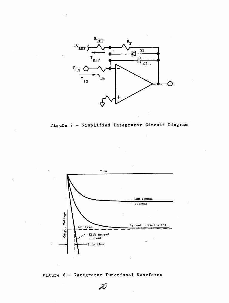
A unique circuit was designed in which an approximation to analog
squaring and integration was accomplished with one operational amp-
lifier. Reference is made to the simplified integrator diagram (fig. 7).
When the input voltage, VIN, is low so that IIN is less than IREF, the
net input to the operational amplifier is negative. The output of this
amplifier, attempting to go positive, is clamped at approximately 0. 5 V
by diode D1; the circuit is now in the off state. When VIN is raised by
an increase in sensed current, IIN can exceed 'REF, with the result
that the output starts going negative as capacitor C2 charges toward
the RF(IREF-IN) with a time constant RFC 2 . This operation is shown
graphically in figure 8. Thus far, this circuit integrates, but does
not square the input voltage.
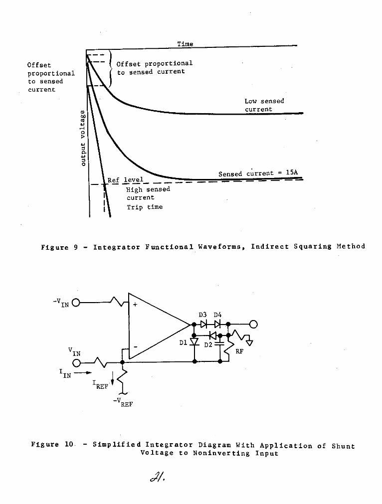
The effect of directly squaring the integrator input voltage would be
to cause higher current-analog voltages to produce a faster trip than
the simplified integrator circuit provides. This same effect is indir-
ectly produced by starting the feedback capacitor charging with the
output already offset in the negative direction by a value of voltage
proportional to the sensed current as shown in the diagram of figure 9.
The voltage offset proportional to the sensed current is obtained
by applying the voltage from the current-sensing shunt directly to the
non-inverting input of the operational amplifier. This circuit diagram
is shown in figure 10.
10
The desired response time versus sensed current is approximated
through appropriate selection of reference voltages, resistance, gains,
and time constant. The fastest allowable response is used, considering
component tolerances and drift. Long delays cause unnecessary heating
of the main SCR; particularly when multiple resets and reclosures of
the SSCB occur. In the preceeding discussion of the integrator circuit,the charging of the feedback capacitor to approximately +0. 5 V in the
off condition has been ignored. The three diodes D2, D3, and D4 pro-
vide compensation for this occurrence.
In the off condition, the output terminal of the bperational ampli-
fier is still at +0. 5 V, but D3 and D4 have insufficient voltage applied
across them to reach the knee of their voltage-current characteristic.
This blocking state leaves a negligible charge on the feedback capacitor
C2, making the output voltage essentially zero.
When IIN exceeds IREF, diode D2 conducts and the feedback cap-
acitor begins to charge. In this case, diode D1 becomes reverse-
biased. Diode D2, in the feedback loop, has a negligible effect on
circuit performance. When IIN is again reduced to less than IREF'the output voltage returns toward zero due to discharge of the feedback
capacitor through diodes D3 and D4 until the output voltage approaches
zero. Because these two diodes are in the feedback loop until diode
D1 clamps the output, diodes D3 and D4 likewise have a negligible
effect on circuit performance.
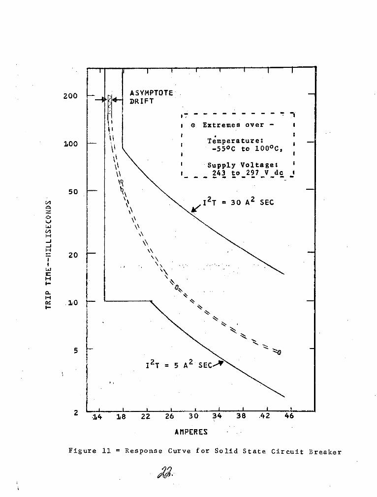
The response of the current sensor and analog circuits is illustra-
ted by the curve of figure 11. The dotted lines with data points included
represent the experimentally determined variation in response over the
extremes of temperature and voltage This total variation of only a
few percent is not only in agreement with theoretically predicted design
limits, but also is well within the I2 t lines at 5 and 30 A 2 . s, which were
initial contract requirements.
11
POWER SUPPLY
The electronic power supply receives its operating voltage from the
270 V dc input line and provides the circuit breaker operating voltages
of ±12 V dc for analog and logic circuits, SCR-1 continuous gate voltage,
-200 V dc for the commutation capacitor precharge and recharge circuit.
While most of the power supply design is conventional, it is critical that
adequate voltage isolation between different portions of the power supply
circuitry be maintained.
LOGIC CIRCUITS
The overall operation of the circuit breaker is controlled by logic
circuitry that relates the time and order of each operational function re-
quired. There are some 14 separate steps or sequences provided as
illustrated by the functional block diagram for the logic portion of the
circuit breaker shown in figure. 12. This circuitry provides the isolation
between control signal inputs and power being controlled as well as all
required timing and counting functions. COSMOS integrated circuits
were chosen for the logic, because of their relatively high noise im-
munity. The number and complexity of the logic functions was a direct
result of the many variable requirements for which feasibility was to
be demonstrated.
BREAKER OPERATION
The logic operation and its control of the breaker is best described
by an overall functional description of the complete circuit breaker. We
refer to the more detailed circuit breaker block diagram in figure 13.for
aid in this description.
A manual close command given to the SSCB causes the power supply
to begin switching. Immediately a 12 V output, fed to the power up-
reset circuitry, sets all logic to the initial state and prevents SCR-1 from
being gated on. Built-in integration circuitry insures a 0. 1 second delay
between the manual close command and the initial clear signal. This delay

12
allows enough time for all critical voltage levels to stabilize. Now,when the initial clear signal arrives, SCR-1 gates on closing the
SSCB into the load.
Before SCR-1 fires, however, the SSCB must be ready to open
under fault-trip conditions in case a short circuit or other overload
condition exists at the load. To insure a readiness for action several
conditions must be set up during the 0. 1 second power up-reset interval.
These conditions are:(1) All power supply output voltages stabilized at operational levels;
(2) All analog and logic circuits armed and ready to respond to
sensed overload and fault-trip output signals;
(3) The commutation circuit ready to commutate with capacitor C1
fully precharged.With the SSCB closed and a load current flowing assume an over-
current, IL, or an I2t fault condition is sensed for the first time. Here's
what happens simultaneously:(1) A trip signal through the comperator fires the SCR-2 gate starting
the commutation cycle;(2) Another signal removes the continuous gate drive from SCR-1;
(3) The programmable timer and the counter reset timer both start
counting time.
When SCR-1 is off and the programmable timer count ends, the
following events happen all at once:
(1) The continuous gate drive is reapplied to SCR-1;
(2) A gate firing pulse is also applied to SCR-1 turning it on;
(3) The recycle counter counts "one".
If the fault still remains on the load, this cycle repeats until either the
fault clears or the recycle counter reaches its programmed count set-
ting.So, if the fault clears, SCR-1 remains on. After 102 seconds the
counter reset timer turns the recycle counter back to zero. A later
fault will then start a complete new cycle.However, if the fault persists and the recycle counter reaches its full
preset count, then SCR-1 remains off. The SSCB is now open and remains

13
so until a manual close command is again applied to it. With the SSCBopen a logic command disables the internal power supply.
SSCB CONSTRUCTION
The circuit breakers are built on a main frame supporting the mainSCR on its heat sink and the individual discrete components of the com-mutation circuit. The majority of the circuitry is placed on three PCboards, one each for the power supply, for the gate and rechargei cir-cuits, and for the analog and logic circuits. The power and gate boardswere conformal-coated because of high voltages. Figure 14 is a photo-graph of the assembled breaker without its cover. Its dimensions areabout 18 cm per side and its weight (cover included) is about 3 kg.
TESTING
The performance of each PC board was measured before it waswired into the final assembly. Timer settings, ultimate current triplevels, and the I2t thresholds were set and calibrated. After completeassembly each breaker was tested operationally as follows:
(1) Response to external close and open commands;(2) Series voltage drop at 15 A;(3) Response time for 12t trip and recycle time;(4) No trip response checked for transient overloads less than pre-
set trip levels.(5) Ultimate trip response measured for 45 A at 243 V and 18 A at
297 V.All tests were run on a special system test tool built for this program.
A simplified schematic of the test tool is shown in figure 15. The results
of the operational tests are shown on the curves of figure 16 to permit easycomparison of the five individual circuit breakers. Please note that thetime to trip for the ultimate current trip tests is, in reality, the timeit took the current to rise to the trip level. This is more a function ofcircuit inductance than of breaker performance. The trip time afterreaching the ultimate trip level was only a few microseconds. Polaroid

14
photographs of oscilloscope traces provided data for recording both
current levels and time to trip.
The total power loss is estimated to be less that 55 watts at full
load, i. e., 270 V and 15 A dc. Of this total 45 watts is due to the 3 V
forward drop at 15 A. The additional 10 watts of loss was not measured,
but is estimated to include power losses in the following circuits: power
supply, SCR-1 continuous gate drive, capacitor recharge, and analog/logic power.
The breakers were characterized by a series of tests in two general
areas:(1) Several 150 V, 10 ps pulses were superimposed on the 270 V dc
line to test transient susceptibility. The breakers did not close
when open and remained closed in the presence of the voltage
transients;(2) Breaker thermal response was measured by testing in a thermal
control chamber at temperatures of 25, 50, 0, -45, 1000 C in
that order. Operational responses were observed and measured
at each temperature setting.Thermal test data is shown in figure 17. One thousand cycle life
tests were made on three breakers, one each at 0, 25, and 500 C. Oper-
ation of two interconnected breakers to form a power transfer switch was
tested with both breakers performing their normal functions. The command
to turn on, with the other breaker on, did result in a break-before-make
operation.
CONCLUSIONS
We have proven the basic feasibility of developing a solid-state cir-
cuit breaker and transfer switch to operate in a 270 V, 15 A dc circuit.
The technology for using SCRs in the solid-state switchgear circuit design
now exists. Circuit breakers using SCR switching elements have been de-
signed, built, and tested. They have met or exceeded most of the originaldesignated performance characteristics. These circuit breakers withtheir automatic trip, their recycle capability, and remote control, can
15
be interconnected to provide a remote controlled transfer switch with
overload protection.
Solid-state switchgear having different current or voltage requirements,
as determined by aircraft or spacecraft electric power system analyses,
can be built using present-day SCR and transistor switching elements. As
further advances are made in power transistors or gate-controlled switches,
simplified circuits can be built to give better performance with less com-
plexity and higher reliability. Improvements in the stability of Hall-
effect devices or linear analog photoisolators could greatly improve
future solid-state breakers. Ultimately remote control by a computer
could replace most of the unique logic circuitry developed in this pro-
gram and thereby simplify the breaker design.
BIBLIOGRAPHY
Waddington, D. and Buchanan, E. Jr.: Study of Feasibility of Solid-
State Electric Switchgear for Aircraft and Spacecraft. NASA CR-
121140, March, 1973.
I IPOKIER ,
I SWITCH CURRENTFROM N ESOURCE
VERLOADPOWER ETECTIONSUPPLY NALOG
I I
D
LOGIC
ON OFF
".---------------- i .. ....... .-- - - - - - - - - - - --
POWER RETURN
Figure 1 - Block Diagram, Logic Controlled Circuit Breaker
C
- +
o Auxiliary SCR
Main SCRVoltage L
supply To LoadSupply
Figure 2.- Direct-Coupled Forced Commutation Circuit
Li SCR 1FROM TO
SOURCE L- OAD
CURRENT
SENSORC. L2
SCR 3 - SCR 4 SCR 2
CAPACITOR
RECHARGE
FIGURE 3 BASIC COiiN-iUTATING CIRCUIT
e +300-Lu
400
a -150,
0'4
I
e +600-74
0o0 I
U
a -450-Lu
to t t2 t3 t4
Figure 4.-.Principal Waveforms of Commutating Circuit

SCR 1+270 Vdc input Tl
SSCR 4 SCR 3 SCR 2
Voltage Decision Isolation
sensing gate switch
Constant currentsource
+
-270 Vdc common
Figure 5.- Recharge Isolation Circuit Functional Diagram
ULTIMATE TRIPSHUNT REFERENCE LEVEL
INVERTING LAMPLIFIER COMPARATOR
TRIP
I I dt COMPARATOR2
I2t
REFERENCE
Figure 6 - Functional Diagram,Analog Fault Detection Circuits
/,
C2.IN
I RIN
Figure 7 - Simplified Integrator Circuit Diagram
Time
Low sensedcurrent
--Ref level Sensed current = 15A
S I High sensedcurrent
-- Trip time
Figure 8 - Integrator Functional Waveforms
Time
Offset ~ Offset proportional
proportional to sensed current
to sensedcurrent
Low sensedacurrent
o0
Sensed current = 15A
Ref level
High sensedcurrent
Trip time
Figure 9 - Integrator Functional Waveforms, Indirect Squaring Method
-VIN+
D3 D4
VIN D DRF
-V-VREF
Figure 10, - Simplified Integrator Diagram With Application of ShuntVoltage to Noninverting Input
'40
200 -- 0ASYMPTOTEDRIFT
i e Extremes over - I
100 Temperature:-550C to 100 0 C,
j\ \o Supply Voltage: D
\\ _ - 243 to 297 V dc
50 \
I2 T = 30 A 2 SEC
I-J
-j.
20
I-
.10
-
12T = 5 A2 SEC--
I I . .a I I i
2 14 18 22 26 30 34 38 .42 46
AMPERES
Figure 11 = Response Curve for Solid State Circuit Breaker

circuit
Recycle Timer SCR 1 gatingcounter gate logic
logicgate logic logic
CRT I and
ExternalRecycle Timer o gate L
program (0 to 9) (1.5 to 100 logic t
counter ms) logic
Counter IL 2treset trip triptimer (CRT) r trip
Clock I I
oscillatorI I Analog I81.92 Hz I curcuit IRecycle I I
counter L.. . -J
-- Power reset logic
supply SCR2SCR2gate logic . External program gate
Power up PowerInitial resetclear circuit supply IPower to logic
to logic - analog, and SCR
Close - SCR1 Continuous gate gate circuitsCommand
Figure 12 - Solid State Circuit Breaker Logic Block Diagram

**
TI~" ____________________
Ti
CAT,
CI
. I-
VE
T'C"
Fiic
I #* 01001 USto Nm CIaMUIt AUAAKts CULT.
FBna
UIassarItews IIr
at Ue Inaue Ccsust
:~r * : :: r suswear sotro Poes meea str, .m ** -
Figure~~~~ 13-Ul~lCll SoidStteCicut rakr untina Da.a

Figure 14 Solid State Circuit Breaker, Covers Removed

Isolation Swit l vichgearunder Test
-I Power
Source Tr n " entr oruGer:r I r n Overl oad (~~~
V(t)1() .009 ill Pnopo
Figure 15. Simplified Schematic, System Test Tool

200:35-A 12t, recycle time
100 ___
1(: 18-A Ultimate, Recycle Time
S- 5040-
30 18-A 12 t, time to trip.
20-
10
_: 35-A I2t, time to trip-
o4
V: Series voltage drop
1.0
0.5-.0.4-
0.3
0.2-
0.2 p: 45-A ultimate, time to trip
S0.05-0.04- X0.03 )
0.02 - :18-A Ultimate Time to Trips
0.01
Unit serial number
Figure 16.- Comparison of Operational Test Data
/747

(0)35-A 12 t, recycle time
(_ ) 45-A ultimate, time to trip
50 -1 _><() 18-A I 2t, time to trip
40
30
20
o() 35-A I2 t, time to trip5
4
( 2 7) Series voltage drop
1.0
Wn0.5
.0.4
0.2
(0) 45 A Ultimate, time to trip
0.1 I-50 -25 0 +25 +50 +75 +100
Temperature, OC
Figure 17.- Variations with Temperature, Serial Number 5Characterization Test