LMV11x Low-Voltage, 45-MHz, Rail-to-Rail Output ... · 2.7V LMV116/ LMV118 OUTPUT 100k : R 1...
28
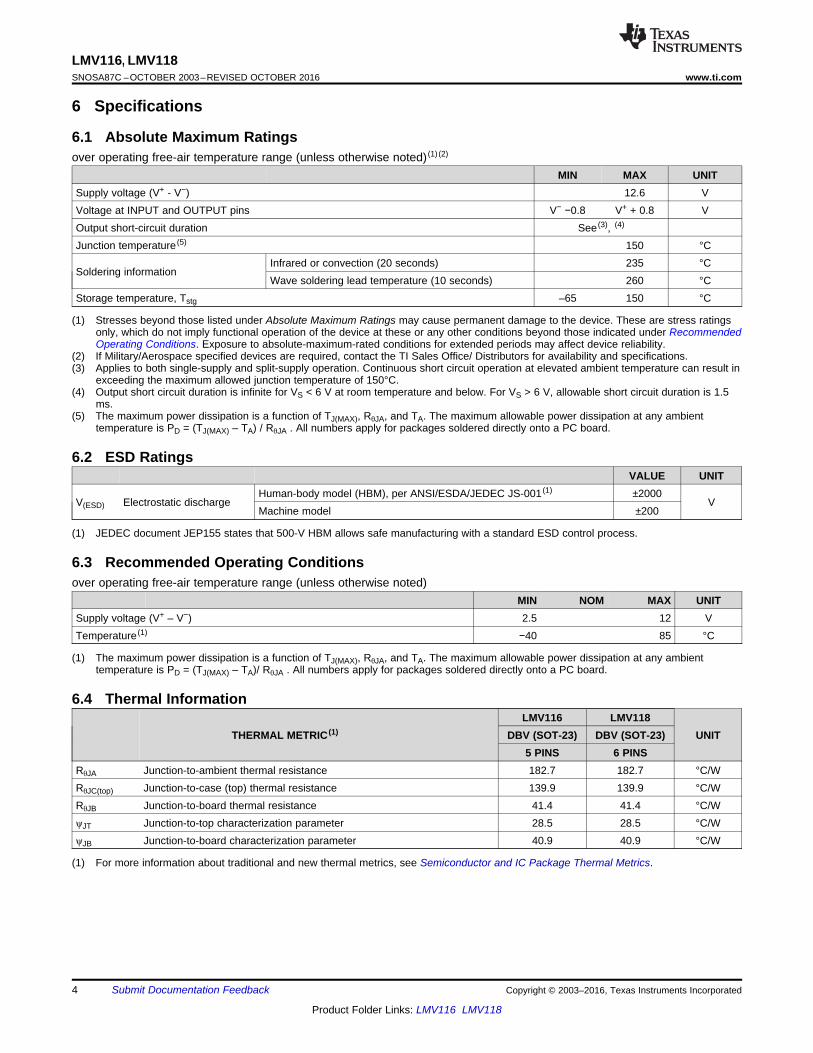
- + 2.7V LMV116/ LMV118 OUTPUT 100k: R 1 15.36MHz SINE WAVE C 1 0.1PF 47k: R 2 Product Folder Sample & Buy Technical Documents Tools & Software Support & Community An IMPORTANT NOTICE at the end of this data sheet addresses availability, warranty, changes, use in safety-critical applications, intellectual property matters and other important disclaimers. PRODUCTION DATA. LMV116, LMV118 SNOSA87C – OCTOBER 2003 – REVISED OCTOBER 2016 LMV11x Low-Voltage, 45-MHz, Rail-To-Rail Output Operational Amplifiers With Shutdown Option 1 1 Features 1• −3-dB BW 45 MHz • Supply Voltage Range 2.7 V to 12 V • Slew Rate 40 V/μs • Supply Current 600 μA • Power Down Supply Current 15 μA • Output Short Circuit Current 32 mA • Linear Output Current ±20 mA • Input Common Mode Voltage −0.3 V to 1.7 V • Output Voltage Swing 20 mV from Rails • Input Voltage Noise 40 nV/√Hz • Input Current Noise 0.75 pA/√Hz 2 Applications • High-Speed Clock Buffer/Driver • Active Filters • High-Speed Portable Devices • Multiplexing Applications (LMV118) • Current Sense Amplifier • High-Speed Transducer Amplifier 3 Description The LMV116 (single) rail-to-rail output voltage feedback amplifiers offer high-speed (45 MHz), and low-voltage operation (2.7 V) in addition to micro- power shutdown capability (LMV118). Output voltage range extends to within 20 mV of either supply rail, allowing wide dynamic range especially in low voltage applications. Even with low supply current of 600 μA, output current capability is kept at a respectable ±20 mA for driving heavier loads. Important device parameters such as BW, slew rate, and output current are kept relatively independent of the operating supply voltage by a combination of process enhancements and design architecture. For portable applications, the LMV118 provides shutdown capability while keeping the turnoff current to 15 μA. Both turnon and turnoff characteristics are well behaved with minimal output fluctuations during transitions, thus the device can be used in power- saving mode, as well as multiplexing applications. Miniature packages (5-pin and 6-pin SOT-23) are further means to ease the adoption of these low- power, high-speed devices in applications where board area is at a premium. Device Information (1) PART NUMBER PACKAGE BODY SIZE (NOM) LMV116 SOT-23 (5) 2.90 mm × 1.60 mm SOT-23 (6) 2.90 mm × 1.60 mm LMV118 SOT-23 (5) 2.90 mm × 1.60 mm SOT-23 (6) 2.90 mm × 1.60 mm (1) For all available packages, see the orderable addendum at the end of the data sheet. Typical Application
Transcript of LMV11x Low-Voltage, 45-MHz, Rail-to-Rail Output ... · 2.7V LMV116/ LMV118 OUTPUT 100k : R 1...
-
+
2.7V
LMV116/
LMV118
OUTPUT
100k:
R115.36MHz
SINE WAVE
C10.1PF
47k:
R2
Product
Folder
Sample &Buy
Technical
Documents
Tools &
Software
Support &Community
An IMPORTANT NOTICE at the end of this data sheet addresses availability, warranty, changes, use in safety-critical applications,intellectual property matters and other important disclaimers. PRODUCTION DATA.
LMV116, LMV118SNOSA87C –OCTOBER 2003–REVISED OCTOBER 2016
LMV11x Low-Voltage, 45-MHz, Rail-To-Rail Output Operational AmplifiersWith Shutdown Option
1
1 Features1• −3-dB BW 45 MHz• Supply Voltage Range 2.7 V to 12 V• Slew Rate 40 V/μs• Supply Current 600 μA• Power Down Supply Current 15 μA• Output Short Circuit Current 32 mA• Linear Output Current ±20 mA• Input Common Mode Voltage −0.3 V to 1.7 V• Output Voltage Swing 20 mV from Rails• Input Voltage Noise 40 nV/√Hz• Input Current Noise 0.75 pA/√Hz
2 Applications• High-Speed Clock Buffer/Driver• Active Filters• High-Speed Portable Devices• Multiplexing Applications (LMV118)• Current Sense Amplifier• High-Speed Transducer Amplifier
3 DescriptionThe LMV116 (single) rail-to-rail output voltagefeedback amplifiers offer high-speed (45 MHz), andlow-voltage operation (2.7 V) in addition to micro-power shutdown capability (LMV118).
Output voltage range extends to within 20 mV ofeither supply rail, allowing wide dynamic rangeespecially in low voltage applications. Even with lowsupply current of 600 μA, output current capability iskept at a respectable ±20 mA for driving heavierloads. Important device parameters such as BW, slewrate, and output current are kept relativelyindependent of the operating supply voltage by acombination of process enhancements and designarchitecture.
For portable applications, the LMV118 providesshutdown capability while keeping the turnoff currentto 15 μA. Both turnon and turnoff characteristics arewell behaved with minimal output fluctuations duringtransitions, thus the device can be used in power-saving mode, as well as multiplexing applications.Miniature packages (5-pin and 6-pin SOT-23) arefurther means to ease the adoption of these low-power, high-speed devices in applications whereboard area is at a premium.
Device Information(1)
PART NUMBER PACKAGE BODY SIZE (NOM)
LMV116SOT-23 (5) 2.90 mm × 1.60 mmSOT-23 (6) 2.90 mm × 1.60 mm
LMV118SOT-23 (5) 2.90 mm × 1.60 mmSOT-23 (6) 2.90 mm × 1.60 mm
(1) For all available packages, see the orderable addendum atthe end of the data sheet.
Typical Application

2
LMV116, LMV118SNOSA87C –OCTOBER 2003–REVISED OCTOBER 2016 www.ti.com
Product Folder Links: LMV116 LMV118
Submit Documentation Feedback Copyright © 2003–2016, Texas Instruments Incorporated
Table of Contents1 Features .................................................................. 12 Applications ........................................................... 13 Description ............................................................. 14 Revision History..................................................... 25 Pin Configuration and Functions ......................... 36 Specifications......................................................... 4
6.1 Absolute Maximum Ratings ...................................... 46.2 ESD Ratings.............................................................. 46.3 Recommended Operating Conditions....................... 46.4 Thermal Information .................................................. 46.5 Electrical Characteristics: 2.7 V ................................ 56.6 Electrical Characteristics: 5 V ................................... 66.7 Electrical Characteristics: ±5 V ................................. 76.8 Typical Characteristics .............................................. 8
7 Detailed Description ............................................ 127.1 Overview ................................................................. 127.2 Functional Block Diagram ....................................... 127.3 Feature Description................................................. 12
7.4 Device Functional Modes........................................ 138 Application and Implementation ........................ 15
8.1 Application Information............................................ 158.2 Typical Application: 2.7-V Single Supply 2:1 MUX 15
9 Power Supply Recommendations ...................... 1610 Layout................................................................... 17
10.1 Layout Guidelines ................................................. 1710.2 Layout Example .................................................... 17
11 Device and Documentation Support ................. 1811.1 Related Documentation......................................... 1811.2 Related Links ........................................................ 1811.3 Receiving Notification of Documentation Updates 1811.4 Community Resources.......................................... 1811.5 Trademarks ........................................................... 1811.6 Electrostatic Discharge Caution............................ 1811.7 Glossary ................................................................ 18
12 Mechanical, Packaging, and OrderableInformation ........................................................... 18
4 Revision HistoryNOTE: Page numbers for previous revisions may differ from page numbers in the current version.
Changes from Revision B (May 2013) to Revision C Page
• Added Device Information and Pin Configuration and Functions sections, ESD Ratings and Thermal Informationtables, Functional Block Diagram, Feature Description, Device Functional Modes, Application and Implementation,Power Supply Recommendations, Layout, Device and Documentation Support, and Mechanical, Packaging, andOrderable Information sections .............................................................................................................................................. 1
• Changed RθJA from 265°C/W to 182.7°C/W ........................................................................................................................... 4
Changes from Revision A (May 2013) to Revision B Page
• Changed layout of National Semiconductor data sheet to TI format.................................................................................... 17

OUTPUT
V-
+IN
V+
-IN
+ -
1
2
3
5
4
OUTPUT
V-
+IN
V+
-IN
+ -
1
2
3
5
4
6
SD
3
LMV116, LMV118www.ti.com SNOSA87C –OCTOBER 2003–REVISED OCTOBER 2016
Product Folder Links: LMV116 LMV118
Submit Documentation FeedbackCopyright © 2003–2016, Texas Instruments Incorporated
5 Pin Configuration and Functions
SOT-23 Package5-Pin DBVTop View
SOT-23 Package6-Pin DBVTop View
Pin FunctionsPIN
I/O DESCRIPTIONNAME LMV116 LMV118+IN 3 3 Input Non-inverting input–IN 4 4 Input Inverting inputOUTPUT 1 1 Output Output
SD — 5 Input Shutdown input. Active high, must be tied to V– with resistor for normaloperation.
V+ 5 6 Power Positive (highest) power supplyV– 2 2 Power Negative (lowest) power supply
4
LMV116, LMV118SNOSA87C –OCTOBER 2003–REVISED OCTOBER 2016 www.ti.com
Product Folder Links: LMV116 LMV118
Submit Documentation Feedback Copyright © 2003–2016, Texas Instruments Incorporated
(1) Stresses beyond those listed under Absolute Maximum Ratings may cause permanent damage to the device. These are stress ratingsonly, which do not imply functional operation of the device at these or any other conditions beyond those indicated under RecommendedOperating Conditions. Exposure to absolute-maximum-rated conditions for extended periods may affect device reliability.
(2) If Military/Aerospace specified devices are required, contact the TI Sales Office/ Distributors for availability and specifications.(3) Applies to both single-supply and split-supply operation. Continuous short circuit operation at elevated ambient temperature can result in
exceeding the maximum allowed junction temperature of 150°C.(4) Output short circuit duration is infinite for VS < 6 V at room temperature and below. For VS > 6 V, allowable short circuit duration is 1.5
ms.(5) The maximum power dissipation is a function of TJ(MAX), RθJA, and TA. The maximum allowable power dissipation at any ambient
temperature is PD = (TJ(MAX) – TA) / RθJA . All numbers apply for packages soldered directly onto a PC board.
6 Specifications
6.1 Absolute Maximum Ratingsover operating free-air temperature range (unless otherwise noted) (1) (2)
MIN MAX UNITSupply voltage (V+ - V−) 12.6 VVoltage at INPUT and OUTPUT pins V− −0.8 V+ + 0.8 VOutput short-circuit duration See (3), (4)
Junction temperature (5) 150 °C
Soldering informationInfrared or convection (20 seconds) 235 °CWave soldering lead temperature (10 seconds) 260 °C
Storage temperature, Tstg –65 150 °C
(1) JEDEC document JEP155 states that 500-V HBM allows safe manufacturing with a standard ESD control process.
6.2 ESD RatingsVALUE UNIT
V(ESD) Electrostatic dischargeHuman-body model (HBM), per ANSI/ESDA/JEDEC JS-001 (1) ±2000
VMachine model ±200
(1) The maximum power dissipation is a function of TJ(MAX), RθJA, and TA. The maximum allowable power dissipation at any ambienttemperature is PD = (TJ(MAX) – TA)/ RθJA . All numbers apply for packages soldered directly onto a PC board.
6.3 Recommended Operating Conditionsover operating free-air temperature range (unless otherwise noted)
MIN NOM MAX UNITSupply voltage (V+ – V−) 2.5 12 VTemperature (1) −40 85 °C
(1) For more information about traditional and new thermal metrics, see Semiconductor and IC Package Thermal Metrics.
6.4 Thermal Information
THERMAL METRIC (1)LMV116 LMV118
UNITDBV (SOT-23) DBV (SOT-23)5 PINS 6 PINS
RθJA Junction-to-ambient thermal resistance 182.7 182.7 °C/WRθJC(top) Junction-to-case (top) thermal resistance 139.9 139.9 °C/WRθJB Junction-to-board thermal resistance 41.4 41.4 °C/WψJT Junction-to-top characterization parameter 28.5 28.5 °C/WψJB Junction-to-board characterization parameter 40.9 40.9 °C/W
5
LMV116, LMV118www.ti.com SNOSA87C –OCTOBER 2003–REVISED OCTOBER 2016
Product Folder Links: LMV116 LMV118
Submit Documentation FeedbackCopyright © 2003–2016, Texas Instruments Incorporated
(1) All limits are specified by testing or statistical analysis.(2) Typical values represent the most likely parametric norm.(3) Offset voltage average drift determined by dividing the change in VOS at temperature extremes into the total temperature change.(4) Positive current corresponds to current flowing into the device.(5) Short-circuit test is a momentary test. See Absolute Maximum Ratings, note 4.(6) Slew rate is the average of the rising and falling slew rates.
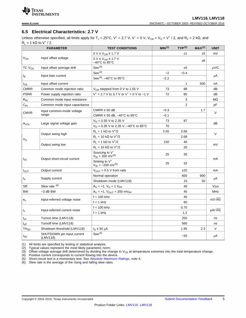
6.5 Electrical Characteristics: 2.7 VUnless otherwise specified, all limits apply for TJ = 25°C, V+ = 2.7 V, V− = 0 V, VCM = VO = V+ / 2, and RF = 2 kΩ, andRL = 1 kΩ to V+ / 2.
PARAMETER TEST CONDITIONS MIN (1) TYP (2) MAX (1) UNIT
VOS Input offset voltage0 V ≤ VCM ≤ 1.7 V ±1 ±5 mV0 V ≤ VCM ≤ 1.7 V–40°C to 85°C ±6
TC VOS Input offset average drift See (3) ±5 μV/C
IB Input bias currentSee (4) −2 −0.4
μASee (4), –40°C to 85°C –2.2
IOS Input offset current 1 500 nACMRR Common mode rejection ratio VCM stepped from 0 V to 1.55 V 73 88 dBPSRR Power supply rejection ratio V+ = 2.7 V to 3.7 V or V− = 0 V to −1 V 72 85 dBRIN Common mode input resistance 3 MΩCIN Common mode input capacitance 2 pF
CMVR Input common-mode voltagerange
CMRR ≥ 50 dB −0.3 1.7V
CMRR ≥ 50 dB, –40°C to 85°C –0.1
AVOL Large signal voltage gainVO = 0.35 V to 2.35 V 73 87
dBVO = 0.35 V to 2.35 V, –40°C to 85°C 70
VO
Output swing highRL = 1 kΩ to V+/2 2.55 2.66
VRL = 10 kΩ to V+/2 2.68
Output swing lowRL = 1 kΩ to V+/2 150 40
mVRL = 10 kΩ to V+/2 20
ISC Output short-circuit current
Sourcing to V−
VID = 200 mV (5) 25 35mA
Sinking to V+
VID = −200 mV (5) 25 32
IOUT Output current VOUT = 0.5 V from rails ±20 mA
IS Supply currentNormal operation 600 900
μAShutdown mode (LMV118) 15 50
SR Slew rate (6) AV = +1, VO = 1 VPP 40 V/μsBW −3 dB BW AV = +1, VOUT = 200 mVPP 45 MHz
en Input-referred voltage noisef = 100 kHz 40
nV/√Hzf = 1 kHz 60
in Input-referred current noisef = 100 kHz 0.75
pA/√Hzf = 1 kHz 1.2
ton Turnon time (LMV118) 250 nstoff Turnoff time (LMV118) 560 nsTHSD Shutdown threshold (LMV118) IS ≤ 50 μA 1.95 2.3 V
ISDSHUTDOWN pin input current(LMV118)
See (4)−20 μA

6
LMV116, LMV118SNOSA87C –OCTOBER 2003–REVISED OCTOBER 2016 www.ti.com
Product Folder Links: LMV116 LMV118
Submit Documentation Feedback Copyright © 2003–2016, Texas Instruments Incorporated
(1) All limits are specified by testing or statistical analysis.(2) Typical values represent the most likely parametric norm.(3) Offset voltage average drift determined by dividing the change in VOS at temperature extremes into the total temperature change.(4) Positive current corresponds to current flowing into the device.(5) Short-circuit test is a momentary test. See Absolute Maximum Ratings, note 4.(6) Slew rate is the average of the rising and falling slew rates.
6.6 Electrical Characteristics: 5 VUnless otherwise specified, all limits apply for TJ = 25°C, V+ = 5 V, V− = 0 V, VCM = VO = V+/2, and RF = 2 kΩ, and RL = 1 kΩto V+/2.
PARAMETER TEST CONDITIONS MIN (1) TYP (2) MAX (1) UNIT
VOS Input offset voltage0 V ≤ VCM ≤ 1.7 V ±1 ±5
mV0 V ≤ VCM ≤ 1.7 V–40°C to 85°C ±6
TC VOS Input offset average drift See (3) ±5 μV/C
IB Input bias currentSee (4) −2 −0.4
μASee (4), –40°C to 85°C –2.2
IOS Input offset current 1 500 nACMRR Common mode rejection ratio VCM stepped from 0 V to 3.8 V 77 85 dBPSRR Power supply rejection ratio V+ = 5 V to 6 V or V− = 0 V to −1 V 72 95 dBRIN Common mode input resistance 3 MΩCIN Common mode input capacitance 2 pF
CMVR Input common-mode voltagerange
CMRR ≥ 50 dB −0.3 4V
CMRR ≥ 50 dB, –40°C to 85°C –0.1
AVOL Large signal voltage gainVO = 1.5 V to 3.5 V 73 87
dBVO = 1.5 V to 3.5 V, –40°C to 85°C 70
VO
Output swing highRL = 1 kΩ to V+/2 4.8 4.95
VRL = 10 kΩ to V+/2 4.98
Output swing lowRL = 1 kΩ to V+/2 200 50
mVRL = 10 kΩ to V+/2 20
ISC Output short-circuit current
Sourcing to V−
VID = 200 mV (5) 35 45mA
Sinking to V+
VID = –200 mV (5) 35 43
IOUT Output current VOUT = 0.5 V from rails ±20 mA
IS Supply currentNormal operation 600 900
μAShutdown mode (LMV118) 10 50
SR Slew rate (6) AV = +1, VO = 1 VPP 40 V/μsBW −3 dB BW AV = +1, VOUT = 200 mVPP 45 MHz
en Input-referred voltage noisef = 100 kHz 40
nV/√Hzf = 1 kHz 60
in Input-referred current noisef = 100 kHz 0.75
pA/√Hzf = 1 kHz 1.2
ton Turnon time (LMV118) 210 nstoff Turnoff time (LMV118) 500 nsTHSD Shutdown threshold (LMV118) IS ≤ 50 μA 4.25 4.6 V
ISDSHUTDOWN pin input current(LMV118)
See (4)−20 μA
7
LMV116, LMV118www.ti.com SNOSA87C –OCTOBER 2003–REVISED OCTOBER 2016
Product Folder Links: LMV116 LMV118
Submit Documentation FeedbackCopyright © 2003–2016, Texas Instruments Incorporated
(1) Typical values represent the most likely parametric norm.(2) Offset voltage average drift determined by dividing the change in VOS. All limits are specified by testing or statistical analysis.(3) at temperature extremes into the total temperature change.(4) Positive current corresponds to current flowing into the device.(5) Short-circuit test is a momentary test. See Absolute Maximum Ratings, note 4.(6) Slew rate is the average of the rising and falling slew rates.
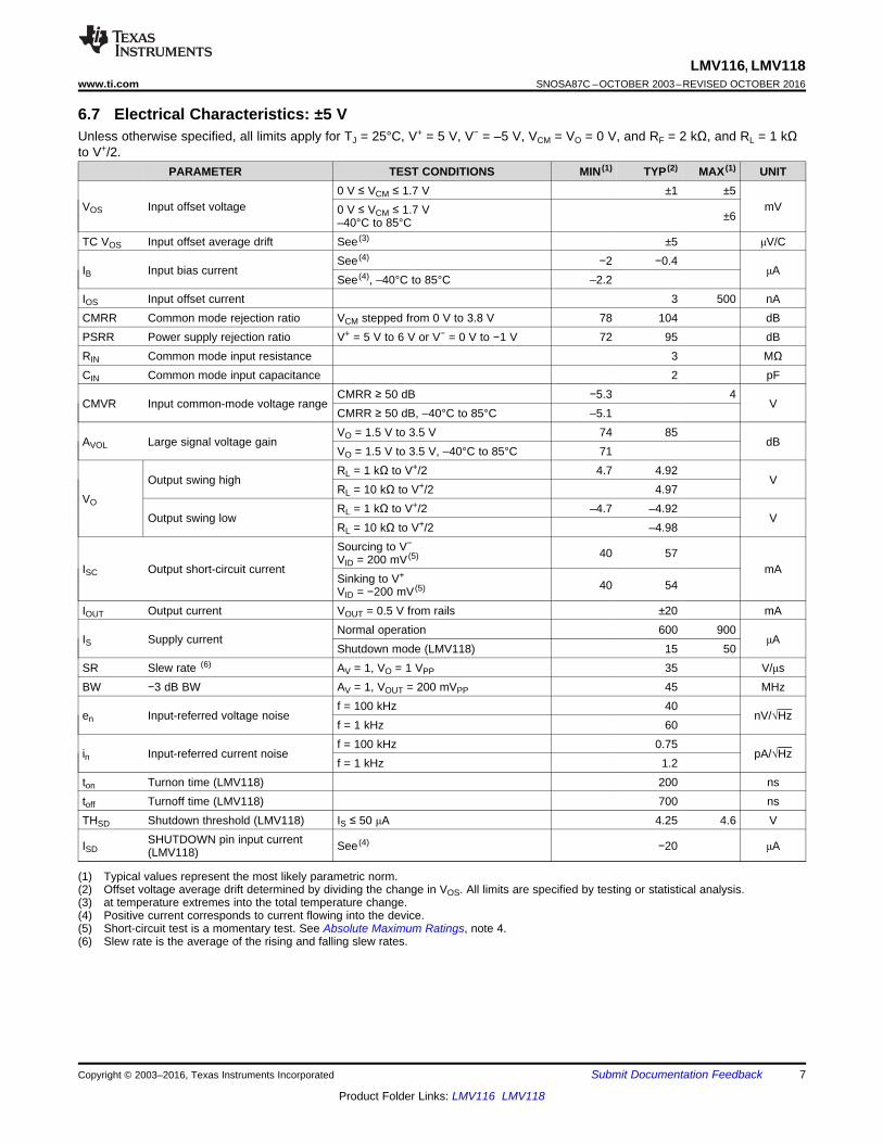
6.7 Electrical Characteristics: ±5 VUnless otherwise specified, all limits apply for TJ = 25°C, V+ = 5 V, V− = –5 V, VCM = VO = 0 V, and RF = 2 kΩ, and RL = 1 kΩto V+/2.
PARAMETER TEST CONDITIONS MIN (1) TYP (2) MAX (1) UNIT
VOS Input offset voltage0 V ≤ VCM ≤ 1.7 V ±1 ±5
mV0 V ≤ VCM ≤ 1.7 V–40°C to 85°C ±6
TC VOS Input offset average drift See (3) ±5 μV/C
IB Input bias currentSee (4) −2 −0.4
μASee (4), –40°C to 85°C –2.2
IOS Input offset current 3 500 nACMRR Common mode rejection ratio VCM stepped from 0 V to 3.8 V 78 104 dBPSRR Power supply rejection ratio V+ = 5 V to 6 V or V− = 0 V to −1 V 72 95 dBRIN Common mode input resistance 3 MΩCIN Common mode input capacitance 2 pF
CMVR Input common-mode voltage rangeCMRR ≥ 50 dB −5.3 4
VCMRR ≥ 50 dB, –40°C to 85°C –5.1
AVOL Large signal voltage gainVO = 1.5 V to 3.5 V 74 85
dBVO = 1.5 V to 3.5 V, –40°C to 85°C 71
VO
Output swing highRL = 1 kΩ to V+/2 4.7 4.92
VRL = 10 kΩ to V+/2 4.97
Output swing lowRL = 1 kΩ to V+/2 –4.7 –4.92
VRL = 10 kΩ to V+/2 –4.98
ISC Output short-circuit current
Sourcing to V−
VID = 200 mV (5) 40 57mA
Sinking to V+
VID = −200 mV (5) 40 54
IOUT Output current VOUT = 0.5 V from rails ±20 mA
IS Supply currentNormal operation 600 900
μAShutdown mode (LMV118) 15 50
SR Slew rate (6) AV = 1, VO = 1 VPP 35 V/μsBW −3 dB BW AV = 1, VOUT = 200 mVPP 45 MHz
en Input-referred voltage noisef = 100 kHz 40
nV/√Hzf = 1 kHz 60
in Input-referred current noisef = 100 kHz 0.75
pA/√Hzf = 1 kHz 1.2
ton Turnon time (LMV118) 200 nstoff Turnoff time (LMV118) 700 nsTHSD Shutdown threshold (LMV118) IS ≤ 50 μA 4.25 4.6 V
ISDSHUTDOWN pin input current(LMV118) See (4) −20 μA

100 10k 10M
FREQUENCY (Hz)
10
50
110
PS
RR
(dB
)
1M100k1k
90
70
30
20
40
60
80
100
+PSRR
-PSRR
VS = ±5V
10 100 1k 10k 100k
FREQUENCY (Hz)
10
100
1000
e n (
nV/Hz)
VOLTAGE
100k 1M 10M 100M
FREQUENCY (Hz)
0
10
30
50
70
GA
IN (
dB)
60
40
20
PH
AS
E (
°)
-20
0
20
40
60
80
100PHASE
GAIN
85°C
-40°C
VS = ±2.5V
RL = 2k
-40°C
85°C
1k 10k 100k 1M 10M
FREQUENCY (Hz)
10
20
30
40
50
60
70
80
90
CM
RR
(dB
)
VS = 5V
-6 -4 -2 0 2 4 6
VCM (V)
0
0.2
0.4
0.6
0.8
1
1.2
1.4
SU
PP
LY C
UR
RE
NT
(m
A)
-40°C
25°C
85°C
1 3 5 7 9 11 12
VS (V)
0.3
0.4
0.5
0.6
0.7
0.8
0.9
I S (
mA
)
-40°C
85°C
25°C
8
LMV116, LMV118SNOSA87C –OCTOBER 2003–REVISED OCTOBER 2016 www.ti.com
Product Folder Links: LMV116 LMV118
Submit Documentation Feedback Copyright © 2003–2016, Texas Instruments Incorporated
6.8 Typical CharacteristicsAt TJ = 25°C. Unless otherwise specified.
Figure 1. Supply Current vs Supply Voltage Figure 2. Supply Current vs VCM
Figure 3. Gain and Phase vs Frequency Figure 4. CMRR vs Frequency
Figure 5. PSRR vs Frequency Figure 6. Input Voltage Noise vs Frequency
0 1 2 3 4 5
0.6
0.7
0.8
0.9
1.0
1.1
1.2
1.3
1.4
VO
S (
mV
)
VCM (V)
-40°C
25°C
85°C
VS = 5V
-40°C
0 0.5 1 1.5 2
0.7
0.8
0.9
1
1.1
1.2
VO
S (
mV
)
VCM (V)
85°C
25°C
VS = 2.7V
100k 1M 10M 100M 200M
GA
IN (
dB)
FREQUENCY (Hz)
PH
AS
E (
°)
0
-2
-4
0
50
100
25°C
85°C
-40°C
PHASE
GAIN
AV = +1
VS = ±5V
RL = 1K
VOUT = 200mVPP
0.2 V/DIV
VS = ±2.5V
RL = 1k:
VOUT = 1VPP
40 ns/DIV
10 100 1k 10k 100k
FREQUENCY (Hz)
0.10
1.00
10.00i n
(pA
/Hz)
CURRENT
100k 1M 10M 200MFREQUENCY (Hz)
-4
-2
0
GA
IN (
dB)
PH
AS
E (
°)
0
50
100
AV = +2
AV = +5
AV = +10
AV = +1GAIN
PHASE
VS = ±5V
RL = 1k:
9
LMV116, LMV118www.ti.com SNOSA87C –OCTOBER 2003–REVISED OCTOBER 2016
Product Folder Links: LMV116 LMV118
Submit Documentation FeedbackCopyright © 2003–2016, Texas Instruments Incorporated
Typical Characteristics (continued)At TJ = 25°C. Unless otherwise specified.
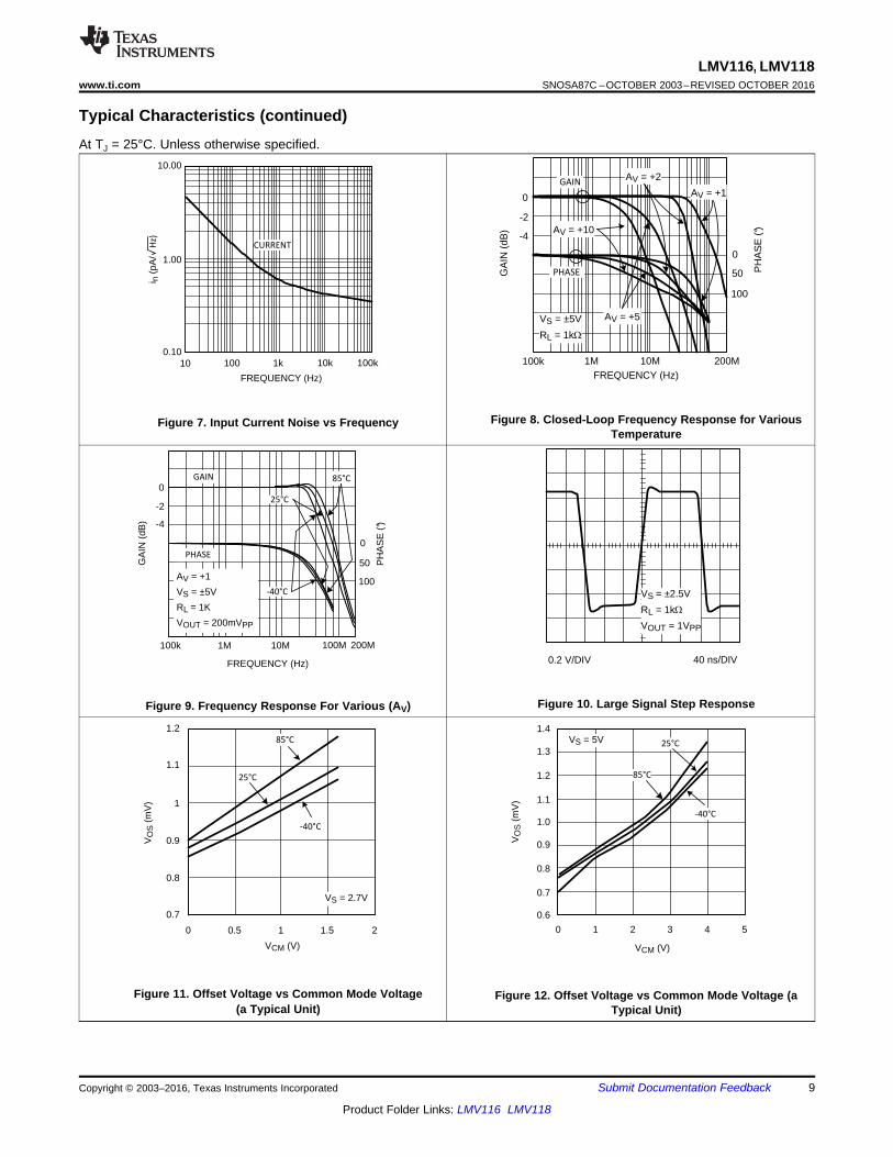
Figure 7. Input Current Noise vs Frequency Figure 8. Closed-Loop Frequency Response for VariousTemperature
Figure 9. Frequency Response For Various (AV) Figure 10. Large Signal Step Response
Figure 11. Offset Voltage vs Common Mode Voltage(a Typical Unit)
Figure 12. Offset Voltage vs Common Mode Voltage (aTypical Unit)

0 0.2 0.4 0.6 0.8 1 1.2 1.4
-5
0
5
10
15
20
25
30
35
40
I SO
UR
CE
(m
A)
VOUT (V)
-40°C
25°C
85°C
VS = 2.7V
-0.5 0 0.5 1 1.5 2 2.5 3
-5
0
5
10
15
20
25
30
35
40
45
I SIN
K (
mA
)
VOUT (V)
-40°C
25°C
85°C
VS = 5V
-5 -3 -1 1 3
VCM (V)
-0.34
-0.32
-0.30
-0.28
-0.26
-0.24
-0.12
INP
UT
BIA
S C
UR
RE
NT
(P
A)
5
-0.22
-0.20
-0.18
-0.16
-0.14
85°C
25°C
-40°C
-0.2 0 0.2 0.4 0.6 0.8 1 1.2 1.4
VOUT (V)
-5
0
5
10
15
20
25
30
35
I SIN
K (
mA
)
-40°C
25°C
85°C
VS = 2.7V
-5 -3.5 -2 -0.5 1 2.5 40.5
0.6
0.7
0.8
0.9
1
1.1
1.2
1.3
1.4
VO
S (
mV
)
VCM (V)
-40°C
85°C
25°CVS = ±5V
0 2 4 6 8 10 12
-0.31
-0.29
-0.27
-0.25
-0.23
-0.21
-0.19
-0.17
-0.15
INP
UT
BIA
S C
UR
RE
NT
(P
A)
SUPPLY VOLTAGE (V)
-40°C
25°C
85°C
10
LMV116, LMV118SNOSA87C –OCTOBER 2003–REVISED OCTOBER 2016 www.ti.com
Product Folder Links: LMV116 LMV118
Submit Documentation Feedback Copyright © 2003–2016, Texas Instruments Incorporated
Typical Characteristics (continued)At TJ = 25°C. Unless otherwise specified.
Figure 13. Offset Voltage vs Common Mode Range(a Typical Unit)
Figure 14. Input Bias Current vs Supply Voltage
Figure 15. Input Bias Current vs VCM Figure 16. Sink Current vs VOUT
Figure 17. Sink Current vs VOUT Figure 18. Souce Current vs VOUT

0 0.5 1 1.5 2 2.5
VOUT (V)
-5
0
5
10
15
20
50
I SO
UR
CE
(m
A)
3
25
30
35
40
45
-40°C
VS = 5V
85°C
25°C
11
LMV116, LMV118www.ti.com SNOSA87C –OCTOBER 2003–REVISED OCTOBER 2016
Product Folder Links: LMV116 LMV118
Submit Documentation FeedbackCopyright © 2003–2016, Texas Instruments Incorporated
Typical Characteristics (continued)At TJ = 25°C. Unless otherwise specified.
Figure 19. Source Current vs VOUT
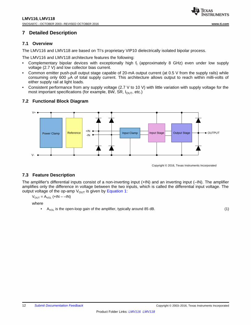
Power Clamp+IN
-INInput Clamp Input Stage Output Stage
V-
V+
OUTPUTReference
Copyright © 2016, Texas Instruments Incorporated
12
LMV116, LMV118SNOSA87C –OCTOBER 2003–REVISED OCTOBER 2016 www.ti.com
Product Folder Links: LMV116 LMV118
Submit Documentation Feedback Copyright © 2003–2016, Texas Instruments Incorporated
7 Detailed Description
7.1 OverviewThe LMV116 and LMV118 are based on TI’s proprietary VIP10 dielectrically isolated bipolar process.
The LMV116 and LMV118 architecture features the following:• Complementary bipolar devices with exceptionally high ft (approximately 8 GHz) even under low supply
voltage (2.7 V) and low collector bias current.• Common emitter push-pull output stage capable of 20-mA output current (at 0.5 V from the supply rails) while
consuming only 600 μA of total supply current. This architecture allows output to reach within milli-volts ofeither supply rail at light loads.
• Consistent performance from any supply voltage (2.7 V to 10 V) with little variation with supply voltage for themost important specifications (for example, BW, SR, IOUT, etc.)
7.2 Functional Block Diagram
7.3 Feature DescriptionThe amplifier's differential inputs consist of a non-inverting input (+IN) and an inverting input (–IN). The amplifieramplifies only the difference in voltage between the two inputs, which is called the differential input voltage. Theoutput voltage of the op-amp VOUT is given by Equation 1:
VOUT = AVOL (+IN – –IN)
where• AVOL is the open-loop gain of the amplifier, typically around 85 dB. (1)
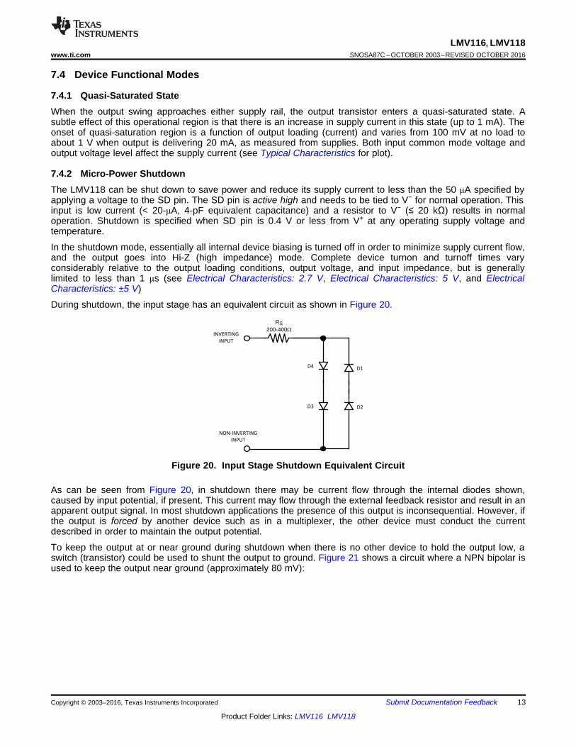
D1
D2D3
D4
NON-INVERTING
INPUT
INVERTING
INPUT
RS200-400:
13
LMV116, LMV118www.ti.com SNOSA87C –OCTOBER 2003–REVISED OCTOBER 2016
Product Folder Links: LMV116 LMV118
Submit Documentation FeedbackCopyright © 2003–2016, Texas Instruments Incorporated
7.4 Device Functional Modes
7.4.1 Quasi-Saturated StateWhen the output swing approaches either supply rail, the output transistor enters a quasi-saturated state. Asubtle effect of this operational region is that there is an increase in supply current in this state (up to 1 mA). Theonset of quasi-saturation region is a function of output loading (current) and varies from 100 mV at no load toabout 1 V when output is delivering 20 mA, as measured from supplies. Both input common mode voltage andoutput voltage level affect the supply current (see Typical Characteristics for plot).
7.4.2 Micro-Power ShutdownThe LMV118 can be shut down to save power and reduce its supply current to less than the 50 μA specified byapplying a voltage to the SD pin. The SD pin is active high and needs to be tied to V− for normal operation. Thisinput is low current (< 20-μA, 4-pF equivalent capacitance) and a resistor to V− (≤ 20 kΩ) results in normaloperation. Shutdown is specified when SD pin is 0.4 V or less from V+ at any operating supply voltage andtemperature.
In the shutdown mode, essentially all internal device biasing is turned off in order to minimize supply current flow,and the output goes into Hi-Z (high impedance) mode. Complete device turnon and turnoff times varyconsiderably relative to the output loading conditions, output voltage, and input impedance, but is generallylimited to less than 1 μs (see Electrical Characteristics: 2.7 V, Electrical Characteristics: 5 V, and ElectricalCharacteristics: ±5 V)
During shutdown, the input stage has an equivalent circuit as shown in Figure 20.
Figure 20. Input Stage Shutdown Equivalent Circuit
As can be seen from Figure 20, in shutdown there may be current flow through the internal diodes shown,caused by input potential, if present. This current may flow through the external feedback resistor and result in anapparent output signal. In most shutdown applications the presence of this output is inconsequential. However, ifthe output is forced by another device such as in a multiplexer, the other device must conduct the currentdescribed in order to maintain the output potential.
To keep the output at or near ground during shutdown when there is no other device to hold the output low, aswitch (transistor) could be used to shunt the output to ground. Figure 21 shows a circuit where a NPN bipolar isused to keep the output near ground (approximately 80 mV):

2 V/DIV 2.00 µs/DIV
VS = 5V
AV = +1
VIN = 3.5VPP
VOUT
SD
SD
RS10k
+
-
Q1
LMV118
5V
VIN
SHUTDOWN
INPUT
VOUT
V-
14
LMV116, LMV118SNOSA87C –OCTOBER 2003–REVISED OCTOBER 2016 www.ti.com
Product Folder Links: LMV116 LMV118
Submit Documentation Feedback Copyright © 2003–2016, Texas Instruments Incorporated
Device Functional Modes (continued)
Figure 21. Active Pulldown Schematic
Figure 22 shows the output waveform.
Figure 22. Output Held Low by Active Pulldown Circuit
If bipolar transistor power dissipation is not tolerable, the switch can be done by an N-channel enhancement-mode MOSFET.

+
-
+
-
LMV118
LMV118
1/5 74HC04
1/574HC04
SELECT INPUT
INPUT A
INPUT B
2k 2k
2k 2k
2.7V
2.7V
SHUTDOWN
SHUTDOWN
RL
15
LMV116, LMV118www.ti.com SNOSA87C –OCTOBER 2003–REVISED OCTOBER 2016
Product Folder Links: LMV116 LMV118
Submit Documentation FeedbackCopyright © 2003–2016, Texas Instruments Incorporated
8 Application and Implementation
NOTEInformation in the following applications sections is not part of the TI componentspecification, and TI does not warrant its accuracy or completeness. TI’s customers areresponsible for determining suitability of components for their purposes. Customers shouldvalidate and test their design implementation to confirm system functionality.
8.1 Application InformationThe LMV11x rail-to-rail output voltage feedback amplifiers offer high-speed (45 MHz) operation with low inputvoltage (2.7 V). Output voltage range extends to within 20 mV of either supply rail, allowing wide dynamic rangeespecially in low voltage applications. Even with low supply current of 600 μA, output current capability is kept ata respectable ±20 mA. For portable applications, the LMV118 provides shutdown capability while keeping theturnoff current to 15 μA. Both turnon and turnoff characteristics are well behaved with minimal output fluctuationsduring transitions which enables the use of LMV118 in multiplexing applications.
8.2 Typical Application: 2.7-V Single Supply 2:1 MUXThe schematic shown in Figure 23 functions as a 2:1 MUX operating on a single 2.7-V power supply, by utilizingthe shutdown feature of the LMV118. Select input signal is connected to the shutdown pin of the first LMV118through 74HC04 inverter. This signal is connected to the shutdown pin of the second LMV118 through anotherinverter. With this setup one of the LMV118 operational amplifiers is always in shutdown mode while the other isin active mode.
Figure 23. 2:1 MUX Operating Off a 2.7-V Single Supply

1 V/DIV 1 µs/DIV
VOUT
SELECT
16
LMV116, LMV118SNOSA87C –OCTOBER 2003–REVISED OCTOBER 2016 www.ti.com
Product Folder Links: LMV116 LMV118
Submit Documentation Feedback Copyright © 2003–2016, Texas Instruments Incorporated
Typical Application: 2.7-V Single Supply 2:1 MUX (continued)8.2.1 Design RequirementsFor typical operational-amplifier applications, use the parameters listed in Table 1.
Table 1. Design ParametersDESIGN PARAMETER EXAMPLE VALUE
Supply voltage 2.7 VLinear output current ±20 mA (typical)
PSRR 85 dB (typical)
8.2.2 Detailed Design ProcedureIt is important to carefully select the values of the external resistors. Choosing large valued external resistorsaffects the closed-loop behavior of the stage because of the interaction of these resistors with parasiticcapacitances. These capacitors could be inherent to the device or a by-product of the board layout andcomponent placement. Either way, keeping the resistor values lower diminishes this interaction. On the otherhand, choosing very low-value resistors could load down nodes and contribute to higher overall powerdissipation.
8.2.3 Application CurveFigure 24 shows the MUX output when selecting between a 1-MHz sine and a 250-kHz triangular waveform.
As can be seen in Figure 24, the output is well behaved, and there are no spikes or glitches due to the switching.Switching times are approximately around 500 ns based on the time when the output is considered valid.
Figure 24. 2:1 MUX Output
9 Power Supply RecommendationsThe LMV11x is specified for operation from 2.7 V to 12 V (±1.35 V to ±6 V) over a –40°C to +85°C temperaturerange. For proper operation, the power supplies must be properly decoupled. For decoupling the supply lines it issuggested that 100-nF capacitors be placed as close as possible to the operational amplifier power supply pins.For single supply, place a capacitor between V+ and V– supply leads. For dual supplies, place one capacitorbetween V+ and ground, and one capacitor between V– and ground.

1
2
3 4
5OUTPUT R1
Via to GND plane
OUTPUT V+
-IN+IN
V-
Supply voltage
R2
C1INPUT
17
LMV116, LMV118www.ti.com SNOSA87C –OCTOBER 2003–REVISED OCTOBER 2016
Product Folder Links: LMV116 LMV118
Submit Documentation FeedbackCopyright © 2003–2016, Texas Instruments Incorporated
10 Layout
10.1 Layout GuidelinesGenerally, a good high-frequency layout keeps power supply and ground traces away from the inverting inputand output pins. Parasitic capacitances on these nodes to ground cause frequency response peaking andpossible circuit oscillations (see OA-15 Frequent Faux Pas in Applying Wideband Current Feedback Amplifiersfor more information).
TI suggests the following evaluation boards as a guide for high-frequency layout and as an aid in device testingand characterization:
DEVICE PACKAGE EVALUATION BOARD P/NLMV116 SOT-23-5 CLC730068LMV118 SOT-23-6 CLC730116
10.2 Layout Example
Figure 25. LMV116/LMV118 Layout
18
LMV116, LMV118SNOSA87C –OCTOBER 2003–REVISED OCTOBER 2016 www.ti.com
Product Folder Links: LMV116 LMV118
Submit Documentation Feedback Copyright © 2003–2016, Texas Instruments Incorporated
11 Device and Documentation Support
11.1 Related DocumentationFor additional information, see the following:
OA-15 Frequent Faux Pas in Applying Wideband Current Feedback Amplifiers
11.2 Related LinksTable 2 lists quick access links. Categories include technical documents, support and community resources,tools and software, and quick access to sample or buy.
Table 2. Related Links
PARTS PRODUCT FOLDER SAMPLE & BUY TECHNICALDOCUMENTS
TOOLS &SOFTWARE
SUPPORT &COMMUNITY
LMV116 Click here Click here Click here Click here Click hereLMV118 Click here Click here Click here Click here Click here
11.3 Receiving Notification of Documentation UpdatesTo receive notification of documentation updates, navigate to the device product folder on ti.com. In the upperright corner, click on Alert me to register and receive a weekly digest of any product information that haschanged. For change details, review the revision history included in any revised document.
11.4 Community ResourcesThe following links connect to TI community resources. Linked contents are provided "AS IS" by the respectivecontributors. They do not constitute TI specifications and do not necessarily reflect TI's views; see TI's Terms ofUse.
TI E2E™ Online Community TI's Engineer-to-Engineer (E2E) Community. Created to foster collaborationamong engineers. At e2e.ti.com, you can ask questions, share knowledge, explore ideas and helpsolve problems with fellow engineers.
Design Support TI's Design Support Quickly find helpful E2E forums along with design support tools andcontact information for technical support.
11.5 TrademarksE2E is a trademark of Texas Instruments.All other trademarks are the property of their respective owners.
11.6 Electrostatic Discharge CautionThese devices have limited built-in ESD protection. The leads should be shorted together or the device placed in conductive foamduring storage or handling to prevent electrostatic damage to the MOS gates.
11.7 GlossarySLYZ022 — TI Glossary.
This glossary lists and explains terms, acronyms, and definitions.
12 Mechanical, Packaging, and Orderable InformationThe following pages include mechanical, packaging, and orderable information. This information is the mostcurrent data available for the designated devices. This data is subject to change without notice and revision ofthis document. For browser-based versions of this data sheet, refer to the left-hand navigation.
PACKAGE OPTION ADDENDUM
www.ti.com 17-Mar-2017
Addendum-Page 1
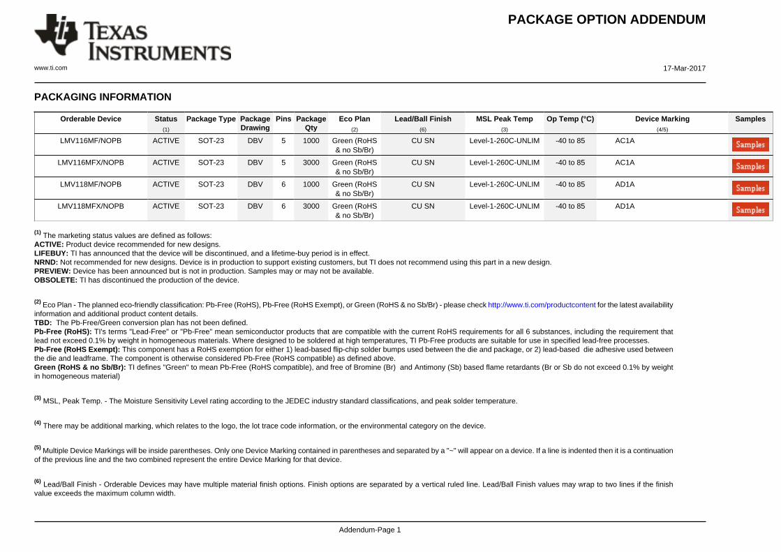
PACKAGING INFORMATION
Orderable Device Status(1)
Package Type PackageDrawing
Pins PackageQty
Eco Plan(2)
Lead/Ball Finish(6)
MSL Peak Temp(3)
Op Temp (°C) Device Marking(4/5)
Samples
LMV116MF/NOPB ACTIVE SOT-23 DBV 5 1000 Green (RoHS& no Sb/Br)
CU SN Level-1-260C-UNLIM -40 to 85 AC1A
LMV116MFX/NOPB ACTIVE SOT-23 DBV 5 3000 Green (RoHS& no Sb/Br)
CU SN Level-1-260C-UNLIM -40 to 85 AC1A
LMV118MF/NOPB ACTIVE SOT-23 DBV 6 1000 Green (RoHS& no Sb/Br)
CU SN Level-1-260C-UNLIM -40 to 85 AD1A
LMV118MFX/NOPB ACTIVE SOT-23 DBV 6 3000 Green (RoHS& no Sb/Br)
CU SN Level-1-260C-UNLIM -40 to 85 AD1A
(1) The marketing status values are defined as follows:ACTIVE: Product device recommended for new designs.LIFEBUY: TI has announced that the device will be discontinued, and a lifetime-buy period is in effect.NRND: Not recommended for new designs. Device is in production to support existing customers, but TI does not recommend using this part in a new design.PREVIEW: Device has been announced but is not in production. Samples may or may not be available.OBSOLETE: TI has discontinued the production of the device.
(2) Eco Plan - The planned eco-friendly classification: Pb-Free (RoHS), Pb-Free (RoHS Exempt), or Green (RoHS & no Sb/Br) - please check http://www.ti.com/productcontent for the latest availabilityinformation and additional product content details.TBD: The Pb-Free/Green conversion plan has not been defined.Pb-Free (RoHS): TI's terms "Lead-Free" or "Pb-Free" mean semiconductor products that are compatible with the current RoHS requirements for all 6 substances, including the requirement thatlead not exceed 0.1% by weight in homogeneous materials. Where designed to be soldered at high temperatures, TI Pb-Free products are suitable for use in specified lead-free processes.Pb-Free (RoHS Exempt): This component has a RoHS exemption for either 1) lead-based flip-chip solder bumps used between the die and package, or 2) lead-based die adhesive used betweenthe die and leadframe. The component is otherwise considered Pb-Free (RoHS compatible) as defined above.Green (RoHS & no Sb/Br): TI defines "Green" to mean Pb-Free (RoHS compatible), and free of Bromine (Br) and Antimony (Sb) based flame retardants (Br or Sb do not exceed 0.1% by weightin homogeneous material)
(3) MSL, Peak Temp. - The Moisture Sensitivity Level rating according to the JEDEC industry standard classifications, and peak solder temperature.
(4) There may be additional marking, which relates to the logo, the lot trace code information, or the environmental category on the device.
(5) Multiple Device Markings will be inside parentheses. Only one Device Marking contained in parentheses and separated by a "~" will appear on a device. If a line is indented then it is a continuationof the previous line and the two combined represent the entire Device Marking for that device.
(6) Lead/Ball Finish - Orderable Devices may have multiple material finish options. Finish options are separated by a vertical ruled line. Lead/Ball Finish values may wrap to two lines if the finishvalue exceeds the maximum column width.

PACKAGE OPTION ADDENDUM
www.ti.com 17-Mar-2017
Addendum-Page 2
Important Information and Disclaimer:The information provided on this page represents TI's knowledge and belief as of the date that it is provided. TI bases its knowledge and belief on informationprovided by third parties, and makes no representation or warranty as to the accuracy of such information. Efforts are underway to better integrate information from third parties. TI has taken andcontinues to take reasonable steps to provide representative and accurate information but may not have conducted destructive testing or chemical analysis on incoming materials and chemicals.TI and TI suppliers consider certain information to be proprietary, and thus CAS numbers and other limited information may not be available for release.
In no event shall TI's liability arising out of such information exceed the total purchase price of the TI part(s) at issue in this document sold by TI to Customer on an annual basis.
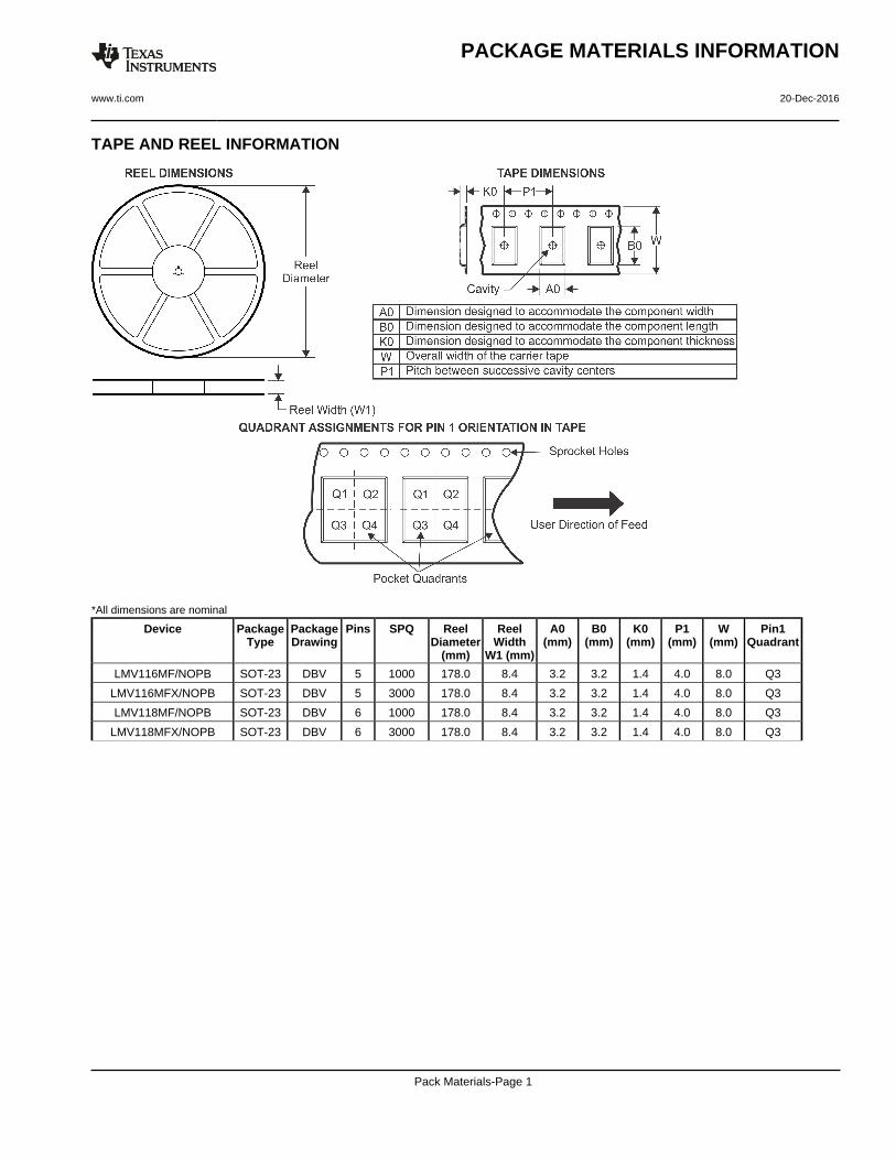
TAPE AND REEL INFORMATION
*All dimensions are nominal
Device PackageType
PackageDrawing
Pins SPQ ReelDiameter
(mm)
ReelWidth
W1 (mm)
A0(mm)
B0(mm)
K0(mm)
P1(mm)
W(mm)
Pin1Quadrant
LMV116MF/NOPB SOT-23 DBV 5 1000 178.0 8.4 3.2 3.2 1.4 4.0 8.0 Q3
LMV116MFX/NOPB SOT-23 DBV 5 3000 178.0 8.4 3.2 3.2 1.4 4.0 8.0 Q3
LMV118MF/NOPB SOT-23 DBV 6 1000 178.0 8.4 3.2 3.2 1.4 4.0 8.0 Q3
LMV118MFX/NOPB SOT-23 DBV 6 3000 178.0 8.4 3.2 3.2 1.4 4.0 8.0 Q3
PACKAGE MATERIALS INFORMATION
www.ti.com 20-Dec-2016
Pack Materials-Page 1
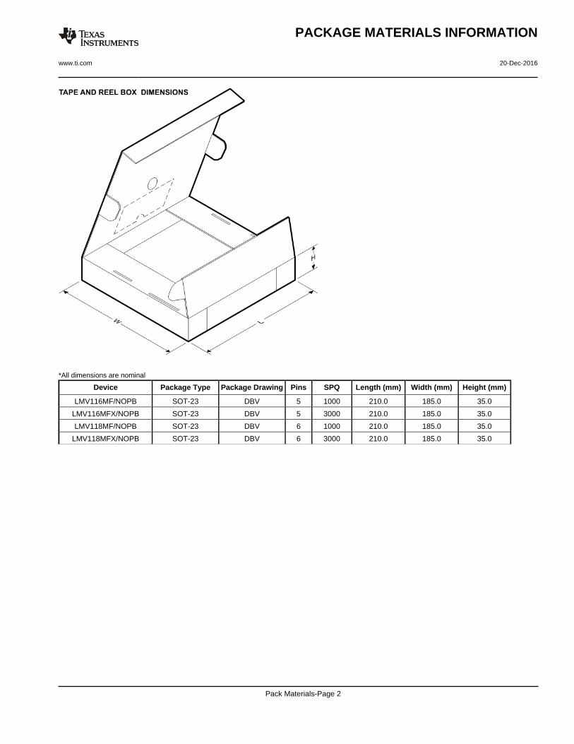
*All dimensions are nominal
Device Package Type Package Drawing Pins SPQ Length (mm) Width (mm) Height (mm)
LMV116MF/NOPB SOT-23 DBV 5 1000 210.0 185.0 35.0
LMV116MFX/NOPB SOT-23 DBV 5 3000 210.0 185.0 35.0
LMV118MF/NOPB SOT-23 DBV 6 1000 210.0 185.0 35.0
LMV118MFX/NOPB SOT-23 DBV 6 3000 210.0 185.0 35.0
PACKAGE MATERIALS INFORMATION
www.ti.com 20-Dec-2016
Pack Materials-Page 2

www.ti.com
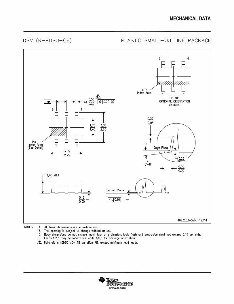
PACKAGE OUTLINE
C
TYP0.220.08
0.25
3.02.6
2X 0.95
1.9
1.45 MAX
TYP0.150.00
5X 0.50.3
TYP0.60.3
TYP80
1.9
A
3.052.75
B1.751.45
(1.1)
SOT-23 - 1.45 mm max heightDBV0005ASMALL OUTLINE TRANSISTOR
4214839/C 04/2017
NOTES: 1. All linear dimensions are in millimeters. Any dimensions in parenthesis are for reference only. Dimensioning and tolerancing per ASME Y14.5M.2. This drawing is subject to change without notice.3. Refernce JEDEC MO-178.
0.2 C A B
1
34
5
2
INDEX AREAPIN 1
GAGE PLANE
SEATING PLANE
0.1 C
SCALE 4.000
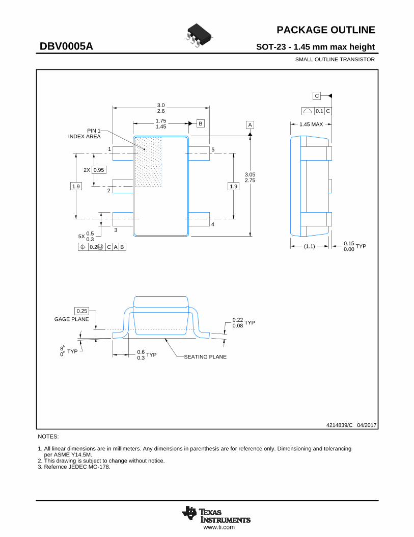
www.ti.com
EXAMPLE BOARD LAYOUT
0.07 MAXARROUND
0.07 MINARROUND
5X (1.1)
5X (0.6)
(2.6)
(1.9)
2X (0.95)
(R0.05) TYP
4214839/C 04/2017
SOT-23 - 1.45 mm max heightDBV0005ASMALL OUTLINE TRANSISTOR
NOTES: (continued) 4. Publication IPC-7351 may have alternate designs. 5. Solder mask tolerances between and around signal pads can vary based on board fabrication site.
SYMM
LAND PATTERN EXAMPLEEXPOSED METAL SHOWN
SCALE:15X
PKG
1
3 4
5
2
SOLDER MASKOPENINGMETAL UNDER
SOLDER MASK
SOLDER MASKDEFINED
EXPOSED METAL
METALSOLDER MASKOPENING
NON SOLDER MASKDEFINED
(PREFERRED)
SOLDER MASK DETAILS
EXPOSED METAL

www.ti.com
EXAMPLE STENCIL DESIGN
(2.6)
(1.9)
2X(0.95)
5X (1.1)
5X (0.6)
(R0.05) TYP
SOT-23 - 1.45 mm max heightDBV0005ASMALL OUTLINE TRANSISTOR
4214839/C 04/2017
NOTES: (continued) 6. Laser cutting apertures with trapezoidal walls and rounded corners may offer better paste release. IPC-7525 may have alternate design recommendations. 7. Board assembly site may have different recommendations for stencil design.
SOLDER PASTE EXAMPLEBASED ON 0.125 mm THICK STENCIL
SCALE:15X
SYMM
PKG
1
3 4
5
2
IMPORTANT NOTICE
Texas Instruments Incorporated (TI) reserves the right to make corrections, enhancements, improvements and other changes to itssemiconductor products and services per JESD46, latest issue, and to discontinue any product or service per JESD48, latest issue. Buyersshould obtain the latest relevant information before placing orders and should verify that such information is current and complete.TI’s published terms of sale for semiconductor products (http://www.ti.com/sc/docs/stdterms.htm) apply to the sale of packaged integratedcircuit products that TI has qualified and released to market. Additional terms may apply to the use or sale of other types of TI products andservices.Reproduction of significant portions of TI information in TI data sheets is permissible only if reproduction is without alteration and isaccompanied by all associated warranties, conditions, limitations, and notices. TI is not responsible or liable for such reproduceddocumentation. Information of third parties may be subject to additional restrictions. Resale of TI products or services with statementsdifferent from or beyond the parameters stated by TI for that product or service voids all express and any implied warranties for theassociated TI product or service and is an unfair and deceptive business practice. TI is not responsible or liable for any such statements.Buyers and others who are developing systems that incorporate TI products (collectively, “Designers”) understand and agree that Designersremain responsible for using their independent analysis, evaluation and judgment in designing their applications and that Designers havefull and exclusive responsibility to assure the safety of Designers' applications and compliance of their applications (and of all TI productsused in or for Designers’ applications) with all applicable regulations, laws and other applicable requirements. Designer represents that, withrespect to their applications, Designer has all the necessary expertise to create and implement safeguards that (1) anticipate dangerousconsequences of failures, (2) monitor failures and their consequences, and (3) lessen the likelihood of failures that might cause harm andtake appropriate actions. Designer agrees that prior to using or distributing any applications that include TI products, Designer willthoroughly test such applications and the functionality of such TI products as used in such applications.TI’s provision of technical, application or other design advice, quality characterization, reliability data or other services or information,including, but not limited to, reference designs and materials relating to evaluation modules, (collectively, “TI Resources”) are intended toassist designers who are developing applications that incorporate TI products; by downloading, accessing or using TI Resources in anyway, Designer (individually or, if Designer is acting on behalf of a company, Designer’s company) agrees to use any particular TI Resourcesolely for this purpose and subject to the terms of this Notice.TI’s provision of TI Resources does not expand or otherwise alter TI’s applicable published warranties or warranty disclaimers for TIproducts, and no additional obligations or liabilities arise from TI providing such TI Resources. TI reserves the right to make corrections,enhancements, improvements and other changes to its TI Resources. TI has not conducted any testing other than that specificallydescribed in the published documentation for a particular TI Resource.Designer is authorized to use, copy and modify any individual TI Resource only in connection with the development of applications thatinclude the TI product(s) identified in such TI Resource. NO OTHER LICENSE, EXPRESS OR IMPLIED, BY ESTOPPEL OR OTHERWISETO ANY OTHER TI INTELLECTUAL PROPERTY RIGHT, AND NO LICENSE TO ANY TECHNOLOGY OR INTELLECTUAL PROPERTYRIGHT OF TI OR ANY THIRD PARTY IS GRANTED HEREIN, including but not limited to any patent right, copyright, mask work right, orother intellectual property right relating to any combination, machine, or process in which TI products or services are used. Informationregarding or referencing third-party products or services does not constitute a license to use such products or services, or a warranty orendorsement thereof. Use of TI Resources may require a license from a third party under the patents or other intellectual property of thethird party, or a license from TI under the patents or other intellectual property of TI.TI RESOURCES ARE PROVIDED “AS IS” AND WITH ALL FAULTS. TI DISCLAIMS ALL OTHER WARRANTIES ORREPRESENTATIONS, EXPRESS OR IMPLIED, REGARDING RESOURCES OR USE THEREOF, INCLUDING BUT NOT LIMITED TOACCURACY OR COMPLETENESS, TITLE, ANY EPIDEMIC FAILURE WARRANTY AND ANY IMPLIED WARRANTIES OFMERCHANTABILITY, FITNESS FOR A PARTICULAR PURPOSE, AND NON-INFRINGEMENT OF ANY THIRD PARTY INTELLECTUALPROPERTY RIGHTS. TI SHALL NOT BE LIABLE FOR AND SHALL NOT DEFEND OR INDEMNIFY DESIGNER AGAINST ANY CLAIM,INCLUDING BUT NOT LIMITED TO ANY INFRINGEMENT CLAIM THAT RELATES TO OR IS BASED ON ANY COMBINATION OFPRODUCTS EVEN IF DESCRIBED IN TI RESOURCES OR OTHERWISE. IN NO EVENT SHALL TI BE LIABLE FOR ANY ACTUAL,DIRECT, SPECIAL, COLLATERAL, INDIRECT, PUNITIVE, INCIDENTAL, CONSEQUENTIAL OR EXEMPLARY DAMAGES INCONNECTION WITH OR ARISING OUT OF TI RESOURCES OR USE THEREOF, AND REGARDLESS OF WHETHER TI HAS BEENADVISED OF THE POSSIBILITY OF SUCH DAMAGES.Unless TI has explicitly designated an individual product as meeting the requirements of a particular industry standard (e.g., ISO/TS 16949and ISO 26262), TI is not responsible for any failure to meet such industry standard requirements.Where TI specifically promotes products as facilitating functional safety or as compliant with industry functional safety standards, suchproducts are intended to help enable customers to design and create their own applications that meet applicable functional safety standardsand requirements. Using products in an application does not by itself establish any safety features in the application. Designers mustensure compliance with safety-related requirements and standards applicable to their applications. Designer may not use any TI products inlife-critical medical equipment unless authorized officers of the parties have executed a special contract specifically governing such use.Life-critical medical equipment is medical equipment where failure of such equipment would cause serious bodily injury or death (e.g., lifesupport, pacemakers, defibrillators, heart pumps, neurostimulators, and implantables). Such equipment includes, without limitation, allmedical devices identified by the U.S. Food and Drug Administration as Class III devices and equivalent classifications outside the U.S.TI may expressly designate certain products as completing a particular qualification (e.g., Q100, Military Grade, or Enhanced Product).Designers agree that it has the necessary expertise to select the product with the appropriate qualification designation for their applicationsand that proper product selection is at Designers’ own risk. Designers are solely responsible for compliance with all legal and regulatoryrequirements in connection with such selection.Designer will fully indemnify TI and its representatives against any damages, costs, losses, and/or liabilities arising out of Designer’s non-compliance with the terms and provisions of this Notice.
Mailing Address: Texas Instruments, Post Office Box 655303, Dallas, Texas 75265Copyright © 2018, Texas Instruments Incorporated