1 MHz to 10 GHz, 55 dB Log Detector/Controller Data Sheet ...
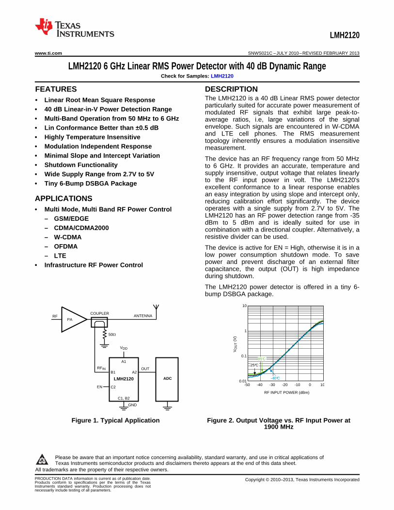
PAANTENNA
RFIN OUT
RF
VDD
GND
50:
ADC
B1
A1
A2
C1, B2
COUPLER
LMH2120
C2EN -50 -40 -30 -20 -10 0 10
10
1
0.1
0.01
RF INPUT POWER (dBm)
VO
UT (
V)
-40°C
25°C
85°C
LMH2120
www.ti.com SNWS021C –JULY 2010–REVISED FEBRUARY 2013
LMH2120 6 GHz Linear RMS Power Detector with 40 dB Dynamic RangeCheck for Samples: LMH2120
1FEATURES DESCRIPTIONThe LMH2120 is a 40 dB Linear RMS power detector
2• Linear Root Mean Square Responseparticularly suited for accurate power measurement of
• 40 dB Linear-in-V Power Detection Range modulated RF signals that exhibit large peak-to-• Multi-Band Operation from 50 MHz to 6 GHz average ratios, i.e, large variations of the signal
envelope. Such signals are encountered in W-CDMA• Lin Conformance Better than ±0.5 dBand LTE cell phones. The RMS measurement• Highly Temperature Insensitive topology inherently ensures a modulation insensitive
• Modulation Independent Response measurement.• Minimal Slope and Intercept Variation The device has an RF frequency range from 50 MHz• Shutdown Functionality to 6 GHz. It provides an accurate, temperature and
supply insensitive, output voltage that relates linearly• Wide Supply Range from 2.7V to 5Vto the RF input power in volt. The LMH2120's• Tiny 6-Bump DSBGA Package excellent conformance to a linear response enablesan easy integration by using slope and intercept only,
APPLICATIONS reducing calibration effort significantly. The deviceoperates with a single supply from 2.7V to 5V. The• Multi Mode, Multi Band RF Power ControlLMH2120 has an RF power detection range from -35– GSM/EDGEdBm to 5 dBm and is ideally suited for use in
– CDMA/CDMA2000 combination with a directional coupler. Alternatively, aresistive divider can be used.– W-CDMA
– OFDMA The device is active for EN = High, otherwise it is in alow power consumption shutdown mode. To save– LTEpower and prevent discharge of an external filter• Infrastructure RF Power Controlcapacitance, the output (OUT) is high impedanceduring shutdown.
The LMH2120 power detector is offered in a tiny 6-bump DSBGA package.
Figure 1. Typical Application Figure 2. Output Voltage vs. RF Input Power at1900 MHz
1
Please be aware that an important notice concerning availability, standard warranty, and use in critical applications ofTexas Instruments semiconductor products and disclaimers thereto appears at the end of this data sheet.
2All trademarks are the property of their respective owners.
PRODUCTION DATA information is current as of publication date. Copyright © 2010–2013, Texas Instruments IncorporatedProducts conform to specifications per the terms of the TexasInstruments standard warranty. Production processing does notnecessarily include testing of all parameters.
LMH2120
SNWS021C –JULY 2010–REVISED FEBRUARY 2013 www.ti.com
These devices have limited built-in ESD protection. The leads should be shorted together or the device placed in conductive foamduring storage or handling to prevent electrostatic damage to the MOS gates.
Absolute Maximum Ratings (1) (2)
Supply Voltage
VDD - GND 5.5V
RF Input
Input power 12 dBm
DC Voltage 1V
Enable (EN) Input Voltage GND-0.4V < VEN and VEN<Min (VDD+0.4, 3.6V)
ESD Tolerance (3)
Human Body Model 2000V
Machine Model 200V
Charge Device Model 1000V
Storage Temperature Range −65°C to 150°C
Junction Temperature (4) 150°C
For soldering specifications:
See product folder at www.ti.com and SNOA549
(1) Absolute Maximum Ratings indicate limits beyond which damage to the device may occur. Operating Ratings indicate conditions forwhich the device is intended to be functional, but specific performance is not ensured. For ensured specifications and the testconditions, see the Electrical Characteristics.
(2) If Military/Aerospace specified devices are required, please contact the Texas Instruments Sales Office/ Distributors for availability andspecifications.
(3) Human body model, applicable std. MIL-STD-883, Method 3015.7. Machine model, applicable std. JESD22–A115–A (ESD MM std ofJEDEC). Field-Induced Charge-Device Model, applicable std. JESD22–C101–C. (ESD FICDM std. of JEDEC)
(4) The maximum power dissipation is a function of TJ(MAX) , θJA. The maximum allowable power dissipation at any ambient temperature isPD = (TJ(MAX) - TA)/θJA. All numbers apply for packages soldered directly into a PC board.
Operating Ratings (1)
Supply Voltage 2.7V to 5V
Temperature Range −40°C to +85°C
RF Frequency Range 50 MHz to 6 GHz
RF Input Power Range −35 dBm to 5 dBm
Package Thermal Resistance θJA(2) 166.7°C/W
(1) Absolute Maximum Ratings indicate limits beyond which damage to the device may occur. Operating Ratings indicate conditions forwhich the device is intended to be functional, but specific performance is not ensured. For ensured specifications and the testconditions, see the Electrical Characteristics.
(2) The maximum power dissipation is a function of TJ(MAX) , θJA. The maximum allowable power dissipation at any ambient temperature isPD = (TJ(MAX) - TA)/θJA. All numbers apply for packages soldered directly into a PC board.
2 Submit Documentation Feedback Copyright © 2010–2013, Texas Instruments Incorporated
Product Folder Links: LMH2120

LMH2120
www.ti.com SNWS021C –JULY 2010–REVISED FEBRUARY 2013
2.7 V and 4.5V DC and AC Electrical CharacteristicsUnless otherwise specified, all limits are ensured to TA = 25°C, VDD = 2.7V and 4.5V (worst case of the 2 is specified), RFIN=1900 MHz CW (Continuous Wave, unmodulated). Boldface limits apply at the temperature extremes (1).
Symbol Parameter Condition Min Typ Max Units(2) (3) (2)
Supply Interface
IDD Supply Current Active mode: EN = High, no signal 3.52.9 mApresent at RFIN. 4.0
Shutdown: EN = LOW, 4.7VBAT = 2.7V 3.8no signal present at 5.0µARFIN 5.7VBAT = 4.5V 4.7 6.1
EN = LOW, RFIN = 0 4.7VBAT = 2.7V 3.8dBm, 1900 MHz 5.0µA
5.7VBAT = 4.5V 4.7 6.1
PSRR Power Supply Rejection Ratio RFIN = -10 dBm, 1900 MHz, 2.7V < 50 60 dBVBAT < 5V
Logic Enable Interface
VLOW EN logic LOW input level 0.6(Shutdown mode) VVHIGH EN logic HIGH input level 1.1
IEN Current into EN pin 50 nA
Input / Output Interface
RIN Input Resistance 44 50 56 ΩVOUT Minimum Output Voltage No Input Signal 2918 mV(Pedestal) 33
ROUT Output Resistance EN = HIGH, RFIN = -10 dBm, 1900 21 ΩMHz, ILOAD = 1 mA, DC measurement 3
IOUT Output Sinking Current RFIN = -10 dBm, 1900 MHz, OUT 30 42connected to 2.5V 25mA
Output Sourcing Current RFIN = -10 dBm, 1900 MHz, OUT 36 45connected to GND 31
IOUT, SD Output Leakage Current in EN = LOW, OUT connected to 2V 80 nAShutdown Mode
en Output Referred Noise (4) RFIN = -10 dBm, 1900 MHz, output 5 µV/√Hzspectrum at 10 kHz
vn Output Referred Noise Integrated Integrated over frequency band 1 kHz - 390 µVRMS(4) 6.5 kHz, RFIN = -10 dBm, 1900 MHz
Timing Characteristics
tON Turn-on Time from shutdown RFIN = -10 dBm, 1900 MHz, EN LOW- 13 18 µsto-HIGH transition to OUT at 90%
tR Rise Time Signal at RFIN from -20 dBm to 0 dBm, 7 µs10% to 90%, 1900 MHz
tF Fall Time Signal at RFIN from 0 dBm to -20 dBm, 18 µs90% to 10%, 1900 MHz
(1) Electrical Table values apply only for factory testing conditions at the temperature indicated. Factory testing conditions result in verylimited self-heating of the device such that TJ = TA. No specification of parametric performance is indicated in the electrical tables underconditions of internal self-heating where TJ > TA.
(2) All limits are ensured by test or statistical analysis.(3) Typical values represent the most likely parametric norm as determined at the time of characterization. Actual typical values may vary
over time and will also depend on the application and configuration. The typical values are not tested and are not specified on shippedproduction material.
(4) This parameter is ensured by design and/or characterization and is not tested in production.
Copyright © 2010–2013, Texas Instruments Incorporated Submit Documentation Feedback 3
Product Folder Links: LMH2120

LMH2120
SNWS021C –JULY 2010–REVISED FEBRUARY 2013 www.ti.com
2.7 V and 4.5V DC and AC Electrical Characteristics (continued)Unless otherwise specified, all limits are ensured to TA = 25°C, VDD = 2.7V and 4.5V (worst case of the 2 is specified), RFIN=1900 MHz CW (Continuous Wave, unmodulated). Boldface limits apply at the temperature extremes (1).
Symbol Parameter Condition Min Typ Max Units(2) (3) (2)
RF Detector Transfer, fit range -15 dBm to -5 dBm for Linear Slope and InterceptRFIN = 50 MHz (5)
PMIN Minimum Power Level, bottom Log Conformance Error within ±1 dB -37end of Dynamic RangedBm
PMAX Maximum Power Level, top end of 4Dynamic Range
VMIN Minimum Output Voltage At PMIN 31 mV
VMAX Maximum Output Voltage At PMAX 2.6 V
KSLOPE Linear Slope 1 dB/dB
PINT Linear Intercept VOUT = 0 dBV -5.7 -5.5 -5.3 dBm
DR Dynamic Range for specified ±1 dB Lin Conformance Error (ELC) 37 41Accuracy 36 40
±3 dB Lin Conformance Error (ELC) 44 48 dB43 47
±0.5 dB Variation over Temperature 41 45(EVOT)
RFIN = 900 MHz (5)
PMIN Minimum Power Level, bottom Lin Conformance Error within ±1 dB -35end of Dynamic RangedBm
PMAX Maximum Power Level, top end of 5Dynamic Range
VMIN Minimum Output Voltage At PMIN 33 mV
VMAX Maximum Output Voltage At PMAX 2.5 V
KSLOPE Linear Slope 1 dB/dB
PINT Linear Intercept VOUT = 0 dBV -4.2 -4.0 -3.8 dBm
DR Dynamic Range for specified ±1 dB Lin Conformance Error (ELC) 36 40Accuracy 33 37
±3 dB Lin Conformance Error (ELC) 45 4844 47
±0.5 dB Variation over Temperature 41 44 dB(EVOT)
±0.3 dB Error for a 1dB Power Step 41(E1dB) 40
±1 dB Error for a 10dB Power Step 45(E10dB)
EMOD Input referred Variation due to W-CDMA Release 6/7/8, 0.15Modulation -35 dBm<RFIN<-3 dBm dBLTE, -35 dBm<RFIN<-3 dBm 0.29
RFIN = 1900 MHz (5)
PMIN Minimum Power Level, bottom Lin Conformance Error within ±1 dB -34end of Dynamic RangedBm
PMAX Maximum Power Level, top end of 4Dynamic Range
VMIN Minimum Output Voltage At PMIN 30 mV
VMAX Maximum Output Voltage At PMAX 1.7 V
KSLOPE Linear Slope 1 dB/dB
PINT Linear Intercept VOUT = 0 dBV -2.2 -1.8 -1.4 dBm
(5) Limits are ensured by design and measurements which are performed on a limited number of samples.
4 Submit Documentation Feedback Copyright © 2010–2013, Texas Instruments Incorporated
Product Folder Links: LMH2120
LMH2120
www.ti.com SNWS021C –JULY 2010–REVISED FEBRUARY 2013
2.7 V and 4.5V DC and AC Electrical Characteristics (continued)Unless otherwise specified, all limits are ensured to TA = 25°C, VDD = 2.7V and 4.5V (worst case of the 2 is specified), RFIN=1900 MHz CW (Continuous Wave, unmodulated). Boldface limits apply at the temperature extremes (1).
Symbol Parameter Condition Min Typ Max Units(2) (3) (2)
DR Dynamic Range for specified ±1 dB Lin Conformance Error (ELC) 35 38Accuracy 31 35
±3 dB Lin Conformance Error (ELC) 44 4841 45
±0.5 dB Variation over Temperature 35 40 dB(EVOT)
±0.3 dB Error for a 1dB Power Step 39(E1dB) 36
±1 dB Error for a 10dB Power Step 35(E10dB)
EMOD Input referred Variation due to W-CDMA Release 6/7/8, 0.16Modulation -34 dBm<RFIN<-2 dBm dBLTE, -34 dBm<RFIN<-2 dBm 0.24
RFIN = 2600 MHz (5)
PMIN Minimum Power Level, bottom Lin Conformance Error within ±1 dB -30end of Dynamic RangedBm
PMAX Maximum Power Level, top end of 6Dynamic Range
VMIN Minimum Output Voltage At PMIN 31 mV
VMAX Maximum Output Voltage At PMAX 1.5 V
KSLOPE Linear Slope 1 dB/dB
PINT Linear Intercept VOUT = 0 dBV 0.8 1.7 2.6 dBm
DR Dynamic Range for specified ±1 dB Lin Conformance Error (ELC) 32 36Accuracy 29 33
±3 dB Lin Conformance Error (ELC) 43 45 dB40 42
±0.5 dB Variation over Temperature 34 39(EVOT)
RFIN = 3500 MHz (6)
PMIN Minimum Power Level, bottom Lin Conformance Error within ±1 dB -26end of Dynamic RangedBm
PMAX Maximum Power Level, top end of 7Dynamic Range
VMIN Minimum Output Voltage At PMIN 32 mV
VMAX Maximum Output Voltage At PMAX 1.1 V
KSLOPE Linear Slope 1 dB/dB
PINT Linear Intercept VOUT = 0 dBV 4.4 5.5 6.7 dBm
DR Dynamic Range for specified ±1 dB Lin Conformance Error (ELC) 30 33Accuracy 27 30
±3 dB Lin Conformance Error (ELC) 39 42 dB36 40
±0.5 dB Variation over Temperature 27 35(EVOT)
(6) Limits are ensured by design and measurements which are performed on a limited number of samples.
Copyright © 2010–2013, Texas Instruments Incorporated Submit Documentation Feedback 5
Product Folder Links: LMH2120
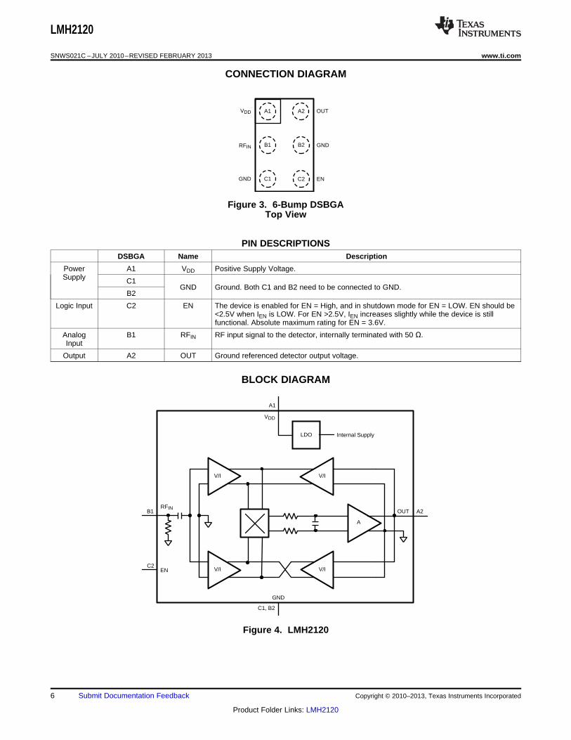
RFINB1 OUT A2
GND
VDD
C1, B2
A1
V/I
V/I
V/I
V/I
A
LDO
C2EN
Internal Supply
OUT
GND
RFIN
VDD A1 A2
B1 B2
C1 C2
GND
EN
LMH2120
SNWS021C –JULY 2010–REVISED FEBRUARY 2013 www.ti.com
CONNECTION DIAGRAM
Figure 3. 6-Bump DSBGATop View
PIN DESCRIPTIONSDSBGA Name Description
Power A1 VDD Positive Supply Voltage.Supply C1
GND Ground. Both C1 and B2 need to be connected to GND.B2
Logic Input C2 EN The device is enabled for EN = High, and in shutdown mode for EN = LOW. EN should be<2.5V when IEN is LOW. For EN >2.5V, IEN increases slightly while the device is stillfunctional. Absolute maximum rating for EN = 3.6V.
Analog B1 RFIN RF input signal to the detector, internally terminated with 50 Ω.Input
Output A2 OUT Ground referenced detector output voltage.
BLOCK DIAGRAM
Figure 4. LMH2120
6 Submit Documentation Feedback Copyright © 2010–2013, Texas Instruments Incorporated
Product Folder Links: LMH2120

RF INPUT POWER (dBm)
OU
TP
UT
SO
UR
CIN
G C
UR
RE
NT
(m
A)
60
50
40
30
20
10
0-50 -40 -30 -20 -10 0 10
85°C
25°C-40°C
RFin = 1900 MHzOUT = 0V
RF INPUT POWER (dBm)
OU
TP
UT
SIN
KIN
G C
UR
RE
NT
(m
A)
60
50
40
30
20
10
0-50 -40 -30 -20 -10 0 10
85°C
25°C -40°C
RFin = 1900 MHzOUT = 2.5V
RF INPUT POWER (dBm)
SU
PP
LY C
UR
RE
NT
(m
A)
6
5
4
3
2
1
0-50 -40 -30 -20 -10 0 10
85°C25°C-40°C
0.5 0.6 0.7 0.8 0.9 1.0 1.1 1.2
5
4
3
2
1
0
ENABLE VOLTAGE (V)
SU
PP
LY C
UR
RE
NT
(m
A)
-40°C
85°C
25°C
0 1 2 3 4 5 6
5
4
3
2
1
0
SUPPLY VOLTAGE (V)
SU
PP
LY C
UR
RE
NT
(m
A)
-40°C
85°C25°C
EN = HIGH
0 1 2 3 4 5 6
8
7
6
5
4
3
2
1
0
SUPPLY VOLTAGE (V)
SU
PP
LY C
UR
RE
NT
(éA)
-40°C
85°C
25°C
EN = LOW
LMH2120
www.ti.com SNWS021C –JULY 2010–REVISED FEBRUARY 2013
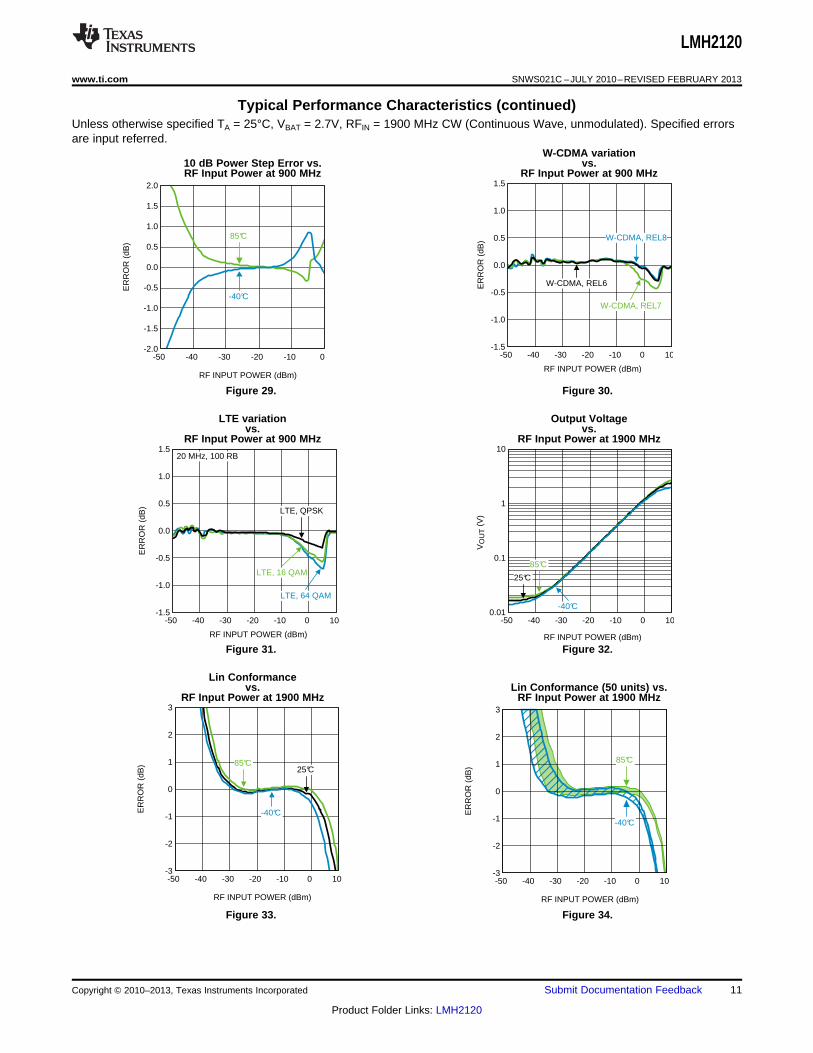
Typical Performance CharacteristicsUnless otherwise specified TA = 25°C, VBAT = 2.7V, RFIN = 1900 MHz CW (Continuous Wave, unmodulated). Specified errors
are input referred.
Supply Current Supply Currentvs. vs.
Supply Voltage (Active) Supply Voltage (Shutdown)
Figure 5. Figure 6.
Supply Current Supply Currentvs. vs.
Enable Voltage (EN) RF Input Power
Figure 7. Figure 8.
Output Sourcing Current Output Sinking Currentvs. vs.
RF Input Power RF Input Power
Figure 9. Figure 10.
Copyright © 2010–2013, Texas Instruments Incorporated Submit Documentation Feedback 7
Product Folder Links: LMH2120

FREQUENCY (Hz)
LIN
INT
ER
CE
PT
(dB
m)
12
10
8
6
4
2
0
-2
-4
-6
-810M 100M 1G 10G
85°C25°C
-40°C
-50 -40 -30 -20 -10 0 10
10
1
0.1
0.01
5.8 GHz
RF INPUT POWER (dBm)
VO
UT (
V)
2.6 GHz
3.5 GHz
50 MHz
900 MHz
1.9 GHz
FREQUENCY (Hz)
LIN
SLO
PE
(dB
/dB
)
1.3
1.2
1.1
1.0
0.9
0.8
0.710M 100M 1G 10G
85°C25°C
-40°C
FREQUENCY (Hz)
OU
TP
UT
VO
LTA
GE
NO
ISE
(P
V/ H
z)
8
7
6
5
4
3
2
1
010 100 1k 10k 100k 1M
PIN = -10 dBm
FREQUENCY (Hz)
RF
INP
UT
IMP
ED
AN
CE
(Ö) 100
755025
0-25-50-75
-100
10M 100M 1G 10G
R
X
MEASURED ON BUMP
100
75
50
25
0
-25
-50
-75
-100
FREQUENCY (Hz)
PS
RR
(dB
)
70
60
50
40
30
20
10
0
10 100 1k 10k 100k
70
60
50
40
30
20
10
0
LMH2120
SNWS021C –JULY 2010–REVISED FEBRUARY 2013 www.ti.com
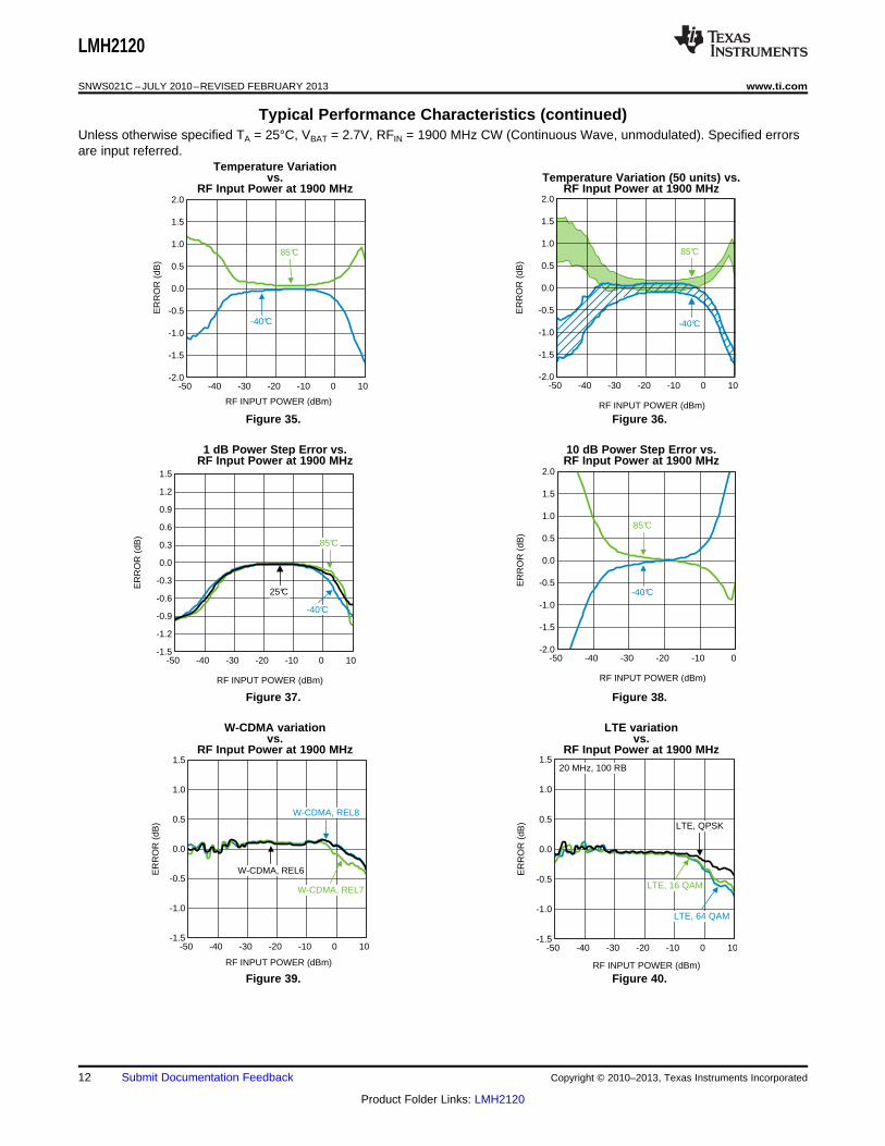
Typical Performance Characteristics (continued)Unless otherwise specified TA = 25°C, VBAT = 2.7V, RFIN = 1900 MHz CW (Continuous Wave, unmodulated). Specified errorsare input referred.
RF Input Impedancevs. Power Supply Rejection Ratio
Frequency, vs.Resistance (R) and Reactance (X) Frequency
Figure 11. Figure 12.
Output Voltage Noise Lin Slopevs. vs.
Frequency Frequency
Figure 13. Figure 14.
Lin Intercept Output Voltagevs. vs.
Frequency RF Input Power
Figure 15. Figure 16.
8 Submit Documentation Feedback Copyright © 2010–2013, Texas Instruments Incorporated
Product Folder Links: LMH2120

RF INPUT POWER (dBm)
ER
RO
R (
dB)
85°C
-40°C
-50 -40 -30 -20 -10 0 10
2.0
1.5
1.0
0.5
0.0
-0.5
-1.0
-1.5
-2.0-50 -40 -30 -20 -10 0 10
2.0
1.5
1.0
0.5
0.0
-0.5
-1.0
-1.5
-2.0
RF INPUT POWER (dBm)
ER
RO
R (
dB)
-40°C
85°C
-50 -40 -30 -20 -10 0 10
3
2
1
0
-1
-2
-3
85°C
RF INPUT POWER (dBm)
ER
RO
R (
dB)
-40°C
25°C
RF INPUT POWER (dBm)
ER
RO
R (
dB)
-50 -40 -30 -20 -10 0 10
3
2
1
0
-1
-2
-3
-40°C
85°C
FREQUENCY (Hz)
VO
UT (
V)
10
1
0.1
0.01
10M 100M 1G 10G
RFIN = -25 dBm
RFIN = -10 dBm
RFIN = -5 dBm
RFIN = 0 dBm
RFIN = -15 dBm
RFIN = -20 dBm
RFIN = -30 dBm
RFIN = -35 dBm
RFIN = -40 dBm
-50 -40 -30 -20 -10 0 10
10
1
0.1
0.01
RF INPUT POWER (dBm)
VO
UT (
V)
-40°C
25°C
85°C
LMH2120
www.ti.com SNWS021C –JULY 2010–REVISED FEBRUARY 2013
Typical Performance Characteristics (continued)Unless otherwise specified TA = 25°C, VBAT = 2.7V, RFIN = 1900 MHz CW (Continuous Wave, unmodulated). Specified errorsare input referred.
Output Voltage Output Voltagevs. vs.
Frequency RF Input Power at 50 MHz
Figure 17. Figure 18.
Lin Conformancevs. Lin Conformance (50 units) vs.
RF Input Power at 50 MHz RF Input Power at 50 MHz
Figure 19. Figure 20.
Temperature Variationvs. Temperature Variation (50 units) vs.
RF Input Power at 50 MHz RF Input Power at 50 MHz
Figure 21. Figure 22.
Copyright © 2010–2013, Texas Instruments Incorporated Submit Documentation Feedback 9
Product Folder Links: LMH2120

-50 -40 -30 -20 -10 0 10
1.5
1.2
0.9
0.6
0.3
0.0
-0.3
-0.6
-0.9
-1.2
-1.5
RF INPUT POWER (dBm)
ER
RO
R (
dB)
-40°C
85°C
25°C
RF INPUT POWER (dBm)
ER
RO
R (
dB)
85°C
-40°C
-50 -40 -30 -20 -10 0 10
2.0
1.5
1.0
0.5
0.0
-0.5
-1.0
-1.5
-2.0
RF INPUT POWER (dBm)
ER
RO
R (
dB)
-50 -40 -30 -20 -10 0 10
3
2
1
0
-1
-2
-3
-40°C
85°C
-50 -40 -30 -20 -10 0 10
2.0
1.5
1.0
0.5
0.0
-0.5
-1.0
-1.5
-2.0
RF INPUT POWER (dBm)
ER
RO
R (
dB)
-40°C
85°C
-50 -40 -30 -20 -10 0 10
3
2
1
0
-1
-2
-3
85°C
RF INPUT POWER (dBm)
ER
RO
R (
dB)
-40°C
25°C
-50 -40 -30 -20 -10 0 10
10
1
0.1
0.01
RF INPUT POWER (dBm)
VO
UT (
V)
-40°C
25°C
85°C
LMH2120
SNWS021C –JULY 2010–REVISED FEBRUARY 2013 www.ti.com
Typical Performance Characteristics (continued)Unless otherwise specified TA = 25°C, VBAT = 2.7V, RFIN = 1900 MHz CW (Continuous Wave, unmodulated). Specified errorsare input referred.
Output Voltage Lin Conformancevs. vs.
RF Input Power at 900 MHz RF Input Power at 900 MHz
Figure 23. Figure 24.
Temperature VariationLin Conformance (50 units) vs. vs.
RF Input Power at 900 MHz RF Input Power at 900 MHz
Figure 25. Figure 26.
Temperature Variation (50 units) vs. 1 dB Power Step Error vs.RF Input Power at 900 MHz RF Input Power at 900 MHz
Figure 27. Figure 28.
10 Submit Documentation Feedback Copyright © 2010–2013, Texas Instruments Incorporated
Product Folder Links: LMH2120
RF INPUT POWER (dBm)
ER
RO
R (
dB)
-50 -40 -30 -20 -10 0 10
3
2
1
0
-1
-2
-3
-40°C
85°C
-50 -40 -30 -20 -10 0 10
3
2
1
0
-1
-2
-3
85°C
RF INPUT POWER (dBm)
ER
RO
R (
dB)
-40°C
25°C
-50 -40 -30 -20 -10 0 10
10
1
0.1
0.01
RF INPUT POWER (dBm)
VO
UT (
V)
-40°C
25°C
85°C
RF INPUT POWER (dBm)
ER
RO
R (
dB)
1.5
1.0
0.5
0.0
-0.5
-1.0
-1.5-50 -40 -30 -20 -10 0 10
LTE, 64 QAM
LTE, 16 QAM
LTE, QPSK
20 MHz, 100 RB
-50 -40 -30 -20 -10 0
2.0
1.5
1.0
0.5
0.0
-0.5
-1.0
-1.5
-2.0
RF INPUT POWER (dBm)
ER
RO
R (
dB)
-40°C
85°C
RF INPUT POWER (dBm)
ER
RO
R (
dB)
1.5
1.0
0.5
0.0
-0.5
-1.0
-1.5-50 -40 -30 -20 -10 0 10
W-CDMA, REL8
W-CDMA, REL7
W-CDMA, REL6
LMH2120
www.ti.com SNWS021C –JULY 2010–REVISED FEBRUARY 2013
Typical Performance Characteristics (continued)Unless otherwise specified TA = 25°C, VBAT = 2.7V, RFIN = 1900 MHz CW (Continuous Wave, unmodulated). Specified errorsare input referred.
W-CDMA variation10 dB Power Step Error vs. vs.RF Input Power at 900 MHz RF Input Power at 900 MHz
Figure 29. Figure 30.
LTE variation Output Voltagevs. vs.
RF Input Power at 900 MHz RF Input Power at 1900 MHz
Figure 31. Figure 32.
Lin Conformancevs. Lin Conformance (50 units) vs.
RF Input Power at 1900 MHz RF Input Power at 1900 MHz
Figure 33. Figure 34.
Copyright © 2010–2013, Texas Instruments Incorporated Submit Documentation Feedback 11
Product Folder Links: LMH2120
RF INPUT POWER (dBm)
ER
RO
R (
dB)
1.5
1.0
0.5
0.0
-0.5
-1.0
-1.5-50 -40 -30 -20 -10 0 10
LTE, 64 QAM
LTE, 16 QAM
LTE, QPSK
20 MHz, 100 RB
RF INPUT POWER (dBm)
ER
RO
R (
dB)
1.5
1.0
0.5
0.0
-0.5
-1.0
-1.5-50 -40 -30 -20 -10 0 10
W-CDMA, REL8
W-CDMA, REL7
W-CDMA, REL6
-50 -40 -30 -20 -10 0 10
1.5
1.2
0.9
0.6
0.3
0.0
-0.3
-0.6
-0.9
-1.2
-1.5
RF INPUT POWER (dBm)
ER
RO
R (
dB)
-40°C
85°C
25°C
-50 -40 -30 -20 -10 0
2.0
1.5
1.0
0.5
0.0
-0.5
-1.0
-1.5
-2.0
RF INPUT POWER (dBm)
ER
RO
R (
dB)
-40°C
85°C
RF INPUT POWER (dBm)
ER
RO
R (
dB)
85°C
-40°C
-50 -40 -30 -20 -10 0 10
2.0
1.5
1.0
0.5
0.0
-0.5
-1.0
-1.5
-2.0-50 -40 -30 -20 -10 0 10
2.0
1.5
1.0
0.5
0.0
-0.5
-1.0
-1.5
-2.0
RF INPUT POWER (dBm)
ER
RO
R (
dB)
-40°C
85°C
LMH2120
SNWS021C –JULY 2010–REVISED FEBRUARY 2013 www.ti.com
Typical Performance Characteristics (continued)Unless otherwise specified TA = 25°C, VBAT = 2.7V, RFIN = 1900 MHz CW (Continuous Wave, unmodulated). Specified errorsare input referred.
Temperature Variationvs. Temperature Variation (50 units) vs.
RF Input Power at 1900 MHz RF Input Power at 1900 MHz
Figure 35. Figure 36.
1 dB Power Step Error vs. 10 dB Power Step Error vs.RF Input Power at 1900 MHz RF Input Power at 1900 MHz
Figure 37. Figure 38.
W-CDMA variation LTE variationvs. vs.
RF Input Power at 1900 MHz RF Input Power at 1900 MHz
Figure 39. Figure 40.
12 Submit Documentation Feedback Copyright © 2010–2013, Texas Instruments Incorporated
Product Folder Links: LMH2120

RF INPUT POWER (dBm)
ER
RO
R (
dB)
85°C
-40°C
-50 -40 -30 -20 -10 0 10
2.0
1.5
1.0
0.5
0.0
-0.5
-1.0
-1.5
-2.0-50 -40 -30 -20 -10 0 10
10
1
0.1
0.01
RF INPUT POWER (dBm)
VO
UT (
V)
-40°C
25°C85°C
RF INPUT POWER (dBm)
ER
RO
R (
dB)
-50 -40 -30 -20 -10 0 10
3
2
1
0
-1
-2
-3
-40°C
85°C
-50 -40 -30 -20 -10 0 10
2.0
1.5
1.0
0.5
0.0
-0.5
-1.0
-1.5
-2.0
RF INPUT POWER (dBm)
ER
RO
R (
dB)
-40°C
85°C
-50 -40 -30 -20 -10 0 10
3
2
1
0
-1
-2
-3
85°C
RF INPUT POWER (dBm)
ER
RO
R (
dB)
-40°C
25°C
-50 -40 -30 -20 -10 0 10
10
1
0.1
0.01
RF INPUT POWER (dBm)
VO
UT (
V)
-40°C
25°C85°C
LMH2120
www.ti.com SNWS021C –JULY 2010–REVISED FEBRUARY 2013
Typical Performance Characteristics (continued)Unless otherwise specified TA = 25°C, VBAT = 2.7V, RFIN = 1900 MHz CW (Continuous Wave, unmodulated). Specified errorsare input referred.
Output Voltage Lin Conformancevs. vs.
RF Input Power at 2600 MHz RF Input Power at 2600 MHz
Figure 41. Figure 42.
Temperature VariationLin Conformance (50 units) vs. vs.
RF Input Power at 2600 MHz RF Input Power at 2600 MHz
Figure 43. Figure 44.
Output VoltageTemperature Variation (50 units) vs. vs.
RF Input Power at 2600 MHz RF Input Power at 3500 MHz
Figure 45. Figure 46.
Copyright © 2010–2013, Texas Instruments Incorporated Submit Documentation Feedback 13
Product Folder Links: LMH2120

-50 -40 -30 -20 -10 0 10
3
2
1
0
-1
-2
-3
85°C
RF INPUT POWER (dBm)
ER
RO
R (
dB)
-40°C
25°C
-50 -40 -30 -20 -10 0 10
10
1
0.1
0.01
RF INPUT POWER (dBm)
VO
UT (
V)
-40°C
25°C85°C
RF INPUT POWER (dBm)
ER
RO
R (
dB)
85°C
-50 -40 -30 -20 -10 0 10
2.0
1.5
1.0
0.5
0.0
-0.5
-1.0
-1.5
-2.0
-40°C
-50 -40 -30 -20 -10 0 10
2.0
1.5
1.0
0.5
0.0
-0.5
-1.0
-1.5
-2.0
RF INPUT POWER (dBm)
ER
RO
R (
dB)
-40°C
85°C
RF INPUT POWER (dBm)
ER
RO
R (
dB)
-50 -40 -30 -20 -10 0 10
3
2
1
0
-1
-2
-3
-40°C
85°C
-50 -40 -30 -20 -10 0 10
3
2
1
0
-1
-2
-3
85°C
RF INPUT POWER (dBm)
ER
RO
R (
dB)
-40°C25°C
LMH2120
SNWS021C –JULY 2010–REVISED FEBRUARY 2013 www.ti.com
Typical Performance Characteristics (continued)Unless otherwise specified TA = 25°C, VBAT = 2.7V, RFIN = 1900 MHz CW (Continuous Wave, unmodulated). Specified errorsare input referred.
Lin Conformancevs. Lin Conformance (50 units) vs.
RF Input Power at 3500 MHz RF Input Power at 3500 MHz
Figure 47. Figure 48.
Temperature Variationvs. Temperature Variation (50 units) vs.
RF Input Power at 3500 MHz RF Input Power at 3500 MHz
Figure 49. Figure 50.
Output Voltage Lin Conformancevs. vs.
RF Input Power at 5800 MHz RF Input Power at 5800 MHz
Figure 51. Figure 52.
14 Submit Documentation Feedback Copyright © 2010–2013, Texas Instruments Incorporated
Product Folder Links: LMH2120
-50 -40 -30 -20 -10 0 10
2.0
1.5
1.0
0.5
0.0
-0.5
-1.0
-1.5
-2.0
RF INPUT POWER (dBm)
ER
RO
R (
dB)
-40°C
85°C
LMH2120
www.ti.com SNWS021C –JULY 2010–REVISED FEBRUARY 2013
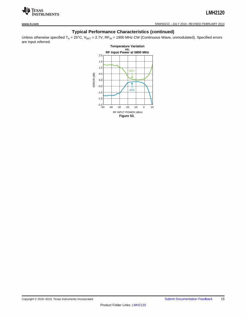
Typical Performance Characteristics (continued)Unless otherwise specified TA = 25°C, VBAT = 2.7V, RFIN = 1900 MHz CW (Continuous Wave, unmodulated). Specified errorsare input referred.
Temperature Variationvs.
RF Input Power at 5800 MHz
Figure 53.
Copyright © 2010–2013, Texas Instruments Incorporated Submit Documentation Feedback 15
Product Folder Links: LMH2120

PAANTENNA
RF
50:
CS
RS
COUPLER
VGA
BASEBAND
GAIN
ADC
EN
OPTIONAL
RFINOUT
VDD
GND
B1A1
A2
B2, C1
LMH2120
C2EN
LMH2120
SNWS021C –JULY 2010–REVISED FEBRUARY 2013 www.ti.com
APPLICATION INFORMATION
The LMH2120 is a 40 dB Linear RMS power detector particularly suited for accurate power measurements ofmodulated RF signals that exhibit large peak-to-average ratios (PAR’s). The RMS detector implements the exactdefinition of power resulting in a power measurement insensitive to high PAR’s. Such signals are encountered,e.g, in LTE and W-CDMA applications. The LMH2120 has an RF frequency range from 50 MHz to 6 GHz. Itprovides an output voltage that relates linearly to the RF input power in volt. Its output voltage is highlyinsensitive to temperature and supply variations.
TYPICAL APPLICATION
The LMH2120 can be used in a wide variety of applications like LTE, W-CDMA, CDMA and GSM. This sectiondiscusses the LMH2120 in a typical transmit power control loop for such applications.
Transmit-power-control-loop circuits make the transmit-power level insensitive to power amplifier (PA)inaccuracy. This is desirable because power amplifiers are non-linear devices and temperature dependent,making it hard to estimate the exact transmit power level. If a control loop is used, the inaccuracy of the PA iseliminated from the overall accuracy of the transmit power level. The accuracy of the transmit power level nowdepends on the RF detector accuracy instead. The LMH2120 is especially suited for transmit-power controlapplications, since it accurately measures transmit power and is insensitive to temperature, supply voltage andmodulation variations.
Figure 54 shows a simplified schematic of a typical transmit-power control system. The output power of the PA ismeasured by the LMH2120 through a directional coupler. The measured output voltage of the LMH2120 isdigitized by the ADC inside the baseband chip. Accordingly, the baseband controls the PA output power level bychanging the gain control signal of the RF VGA. Although the output ripple of the LMH2120 is typically lowenough, an optional low-pass filter can be placed in between the LMH2120 and the ADC to further reduce theripple.
Figure 54. Transmit-Power Control System
ACCURATE POWER MEASUREMENT
Detectors have evolved over the years along with the communication standards. Newer communicationstandards like LTE and W-CDMA raise the need for more advanced accurate power detectors. To be able todistinguish the various detector types it is important to understand what the ideal power measurement shouldlook like and how a power measurement is implemented.
Power is a metric for the average energy content of a signal. By definition it is not a function of the signal shapeover time. In other words, the power content of a 0 dBm sine wave is identical to the power content of a 0 dBmsquare wave or a 0 dBm W-CDMA signal; all these signals have the same average power content.
The average power can be described by the following formula:
16 Submit Documentation Feedback Copyright © 2010–2013, Texas Instruments Incorporated
Product Folder Links: LMH2120

v(t)2dt³1T
VRMS =
P = dt =T1 T
0³v(t)2
R
VRMS2
R
LMH2120
www.ti.com SNWS021C –JULY 2010–REVISED FEBRUARY 2013
(1)
where T is the time interval over which is averaged, v(t) is the instantaneous voltage at time t, R is the resistancein which the power is dissipated, and VRMS is the equivalent RMS voltage.
According to aforementioned formula for power, an exact power measurement can be done by measuring theRMS voltage (VRMS) of a signal. The RMS voltage is described by:
(2)
Implementing the exact formula for RMS can be difficult however. A simplification can be made in determiningthe average power when information about the waveform is available. If the signal shape is known, therelationship between RMS value and, for instance, the peak value of the RF signal is also known. It thus enablesa measurement based on measuring peak voltage rather than measuring the RMS voltage. To calculate theRMS value (and therewith the average power), the measured peak voltage is translated into an RMS voltagebased on the waveform characteristics. A few examples:• Sine wave: VRMS = VPEAK / √2• Square wave: VRMS = VPEAK
• Saw-tooth wave: VRMS = VPEAK / √3
For more complex waveforms it is not always easy to determine the exact relationship between RMS value andpeak value. A peak measurement can therefore become impractical. An approximation can be used for the VRMSto VPEAK relationship, but it can result in a less accurate average power estimate.
Depending on the detection mechanism, power detectors may produce a slightly different output signal inresponse to the earlier mentioned waveforms, even though the average power level of these signals are thesame. This error is due to the fact that not all power detectors strictly implement the definition for signal power,being the root mean square (RMS) of the signal. To cover for the systematic error in the output response of adetector, calibration can be used. After calibration a look-up table corrects for the error. Multiple look-up tablescan be created for different modulation schemes.
TYPES OF RF DETECTORS
This section provides an overview of detectors based on their detection principle. Detectors that will be discussedare:• Peak Detectors• LOG Amp Detectors• RMS Detectors
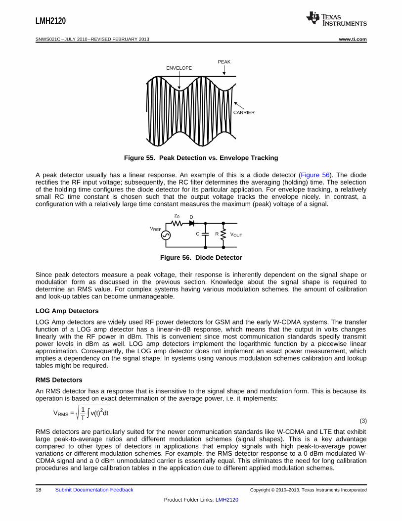
Peak Detectors
A peak detector is one of the simplest type of detector, storing the highest value arising in a certain time window.However, a peak detector is typically used with a relatively long holding time when compared to the carrierfrequency and a relatively short holding time with respect to the envelope frequency. In this way a peak detectoris used as AM demodulator or envelope tracker (Figure 55).
Copyright © 2010–2013, Texas Instruments Incorporated Submit Documentation Feedback 17
Product Folder Links: LMH2120
v(t)2dt³1T
VRMS =
C R VOUT
Z0 D
VREF
CARRIER
PEAKENVELOPE
LMH2120
SNWS021C –JULY 2010–REVISED FEBRUARY 2013 www.ti.com
Figure 55. Peak Detection vs. Envelope Tracking
A peak detector usually has a linear response. An example of this is a diode detector (Figure 56). The dioderectifies the RF input voltage; subsequently, the RC filter determines the averaging (holding) time. The selectionof the holding time configures the diode detector for its particular application. For envelope tracking, a relativelysmall RC time constant is chosen such that the output voltage tracks the envelope nicely. In contrast, aconfiguration with a relatively large time constant measures the maximum (peak) voltage of a signal.
Figure 56. Diode Detector
Since peak detectors measure a peak voltage, their response is inherently dependent on the signal shape ormodulation form as discussed in the previous section. Knowledge about the signal shape is required todetermine an RMS value. For complex systems having various modulation schemes, the amount of calibrationand look-up tables can become unmanageable.
LOG Amp Detectors
LOG Amp detectors are widely used RF power detectors for GSM and the early W-CDMA systems. The transferfunction of a LOG amp detector has a linear-in-dB response, which means that the output in volts changeslinearly with the RF power in dBm. This is convenient since most communication standards specify transmitpower levels in dBm as well. LOG amp detectors implement the logarithmic function by a piecewise linearapproximation. Consequently, the LOG amp detector does not implement an exact power measurement, whichimplies a dependency on the signal shape. In systems using various modulation schemes calibration and lookuptables might be required.
RMS Detectors
An RMS detector has a response that is insensitive to the signal shape and modulation form. This is because itsoperation is based on exact determination of the average power, i.e. it implements:
(3)
RMS detectors are particularly suited for the newer communication standards like W-CDMA and LTE that exhibitlarge peak-to-average ratios and different modulation schemes (signal shapes). This is a key advantagecompared to other types of detectors in applications that employ signals with high peak-to-average powervariations or different modulation schemes. For example, the RMS detector response to a 0 dBm modulated W-CDMA signal and a 0 dBm unmodulated carrier is essentially equal. This eliminates the need for long calibrationprocedures and large calibration tables in the application due to different applied modulation schemes.
18 Submit Documentation Feedback Copyright © 2010–2013, Texas Instruments Incorporated
Product Folder Links: LMH2120
iLF2dt =³ iRF
2dt³
iOUT = I0
iLF2 - iRF
2
RFINB1 OUT A2
GND
VDD
C1, B2
A1
V/I
V/I
V/I
V/I
A
LDO
C2EN
Internal Supply
i1
i2
iOUT VOUT
LMH2120
www.ti.com SNWS021C –JULY 2010–REVISED FEBRUARY 2013
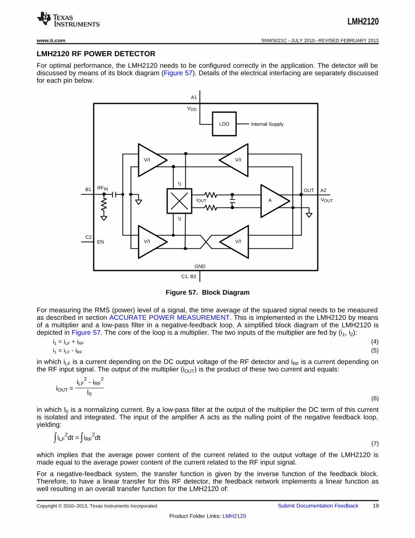
LMH2120 RF POWER DETECTOR
For optimal performance, the LMH2120 needs to be configured correctly in the application. The detector will bediscussed by means of its block diagram (Figure 57). Details of the electrical interfacing are separately discussedfor each pin below.
Figure 57. Block Diagram
For measuring the RMS (power) level of a signal, the time average of the squared signal needs to be measuredas described in section ACCURATE POWER MEASUREMENT. This is implemented in the LMH2120 by meansof a multiplier and a low-pass filter in a negative-feedback loop. A simplified block diagram of the LMH2120 isdepicted in Figure 57. The core of the loop is a multiplier. The two inputs of the multiplier are fed by (i1, i2):
i1 = iLF + iRF (4)i1 = iLF - iRF (5)
in which iLF is a current depending on the DC output voltage of the RF detector and iRF is a current depending onthe RF input signal. The output of the multiplier (iOUT) is the product of these two current and equals:
(6)
in which I0 is a normalizing current. By a low-pass filter at the output of the multiplier the DC term of this currentis isolated and integrated. The input of the amplifier A acts as the nulling point of the negative feedback loop,yielding:
(7)
which implies that the average power content of the current related to the output voltage of the LMH2120 ismade equal to the average power content of the current related to the RF input signal.
For a negative-feedback system, the transfer function is given by the inverse function of the feedback block.Therefore, to have a linear transfer for this RF detector, the feedback network implements a linear function aswell resulting in an overall transfer function for the LMH2120 of:
Copyright © 2010–2013, Texas Instruments Incorporated Submit Documentation Feedback 19
Product Folder Links: LMH2120

AdB = 20LOG 1 +R1
RIN»¼
º«¬
ª
PAANTENNA
RFIN OUT
RF
VDD
GND
ADC
B1
A1
A2
B2, C1
LMH2120
C2EN
R1
³VOUT = k vRF2dt
LMH2120
SNWS021C –JULY 2010–REVISED FEBRUARY 2013 www.ti.com
(8)
in which k is the conversion gain. Note that as a result of the feedback loop a square root is also implemented,yielding the RMS function.
Given this architecture for the RF detector, the high performance of the LMH2120 can be understood. In theorythe accuracy of the linear transfer is set by:• The linear feedback network, which basically needs to process a DC signal only.• A high loop gain for the feedback loop, which is ensured by the amplifier gain A.
The RMS functionality is inherent to the feedback loop and the use of a multiplier. Thus, a very accurate LIN-RMS RF power detector is obtained.
To ensure a low dependency on the supply voltage, the internal detector circuitry is supplied via a low drop-out(LDO) regulator. This enables the usage of a wide range of supply voltage (2.7V to 5V) in combination with a lowsensitivity of the output signal for the external supply voltage.
RF Input
RF systems typically use a characteristic impedance of 50Ω; the LMH2120 is no exception to this. The RF inputpin of the LMH2120 has an input impedance of 50Ω. It enables an easy, direct connection to a directionalcoupler without the need for additional components (Figure 54). For an accurate power measurement the inputpower range of the LMH2120 needs to be aligned with the output power range of the power amplifier. This canbe done by selecting a directional coupler with the appropriate coupling factor.
Since the LMH2120 has a constant input impedance, a resistive divider can also be used instead of a directionalcoupler (Figure 58).
Figure 58. Application with Resistive Divider
Resistor R1 implements an attenuator, together with the detector input impedance, to match the output range ofthe PA with the input range of the LMH2120. The attenuation (AdB) realized by R1 and the effective inputimpedance (RIN) of the LMH2120 equals:
(9)
Solving this expression for R1 yields:
20 Submit Documentation Feedback Copyright © 2010–2013, Texas Instruments Incorporated
Product Folder Links: LMH2120

RFIN OUT
LMH2120
VDD
GND
ENADC
B1
CS
RSA1 A2
B2,C1C2
-
+
10R1 = - 1 RIN»¼
º«¬
ªAdB
20
LMH2120
www.ti.com SNWS021C –JULY 2010–REVISED FEBRUARY 2013
(10)
Suppose the desired attenuation is 30 dB with a given LMH2120 input impedance of 50Ω, the resistor R1 needsto be 1531Ω. A practical value is 1.5 kΩ. Although this is a cheaper solution than the application with directionalcoupler, it has a disadvantage. After calculating the resistor value it is possible that the realized attenuation isless than expected. This is because of the parasitic capacitance of resistor R1 which results in a lower actualrealized attenuation. Whether the attenuation will be reduced depends on the frequency of the RF signal and theparasitic capacitance of resistor R1. Since the parasitic capacitance varies from resistor to resistor, exactdetermination of the realized attenuation can be difficult. A way to reduce the parasitic capacitance of resistor R1is to realize it as a series connection of several separate resistors.
Enable
To save power, the LMH2120 can be brought into a low-power shutdown mode by means of the enable pin (EN).The device is active for EN = HIGH (VEN > 1.1V), and in the low-power shutdown mode for EN = LOW (VEN <0.6V). In this state the output of the LMH2120 is switched to high-impedance. This high impedance prevents thedischarge of the optional low-pass filter which is good for power efficiency. Using the shutdown function, caremust be taken not to exceed the absolute maximum ratings. Since the device has an internal operating voltage of2.5V, the voltage level on the enable should not be higher than 3V to prevent excess current flowing into theenable pin. Also enable voltage levels lower than 400 mV below GND should be prevented. In both cases theESD devices start to conduct when the enable voltage range is exceeded and excess current will be drawn. Acorrect operation is not ensured then. The absolute maximum ratings are also exceeded when EN is switched toHIGH (from shutdown to active mode) while the supply voltage is switched off. This situation should be preventedat all times. A possible solution to protect the device is to add a resistor of 1 kΩ in series with the enable input tolimit the current.
Output
The output of the LMH2120 provides a DC voltage that is a measure for the applied RF power to the input pin.The output voltage has a linear-in-V response for an applied RF signal.
RF power detectors can have some residual ripple on the output due to the modulation of the applied RF signal.The residual ripple on the LMH2120’s output is small; therefore, additional filtering is usually not needed. This isbecause its internal averaging mechanism reduces the ripple significantly. For some modulation types havingvery high peak-to-average ratios or low-frequency components in the amplitude modulation, additional filteringmight be useful.
Filtering can be applied by an external low-pass filter. It should be realized that filtering reduces not only theripple, but also increases the response time. In other words, it takes longer before the output reaches its finalvalue. A trade-off should be made between allowed ripple and allowed response time. The filtering technique isdepicted in Figure 59. The low-pass output filter is realized by resistor RS and capacitor CS. The -3 dB bandwidthof this filter can be calculated by:
f−3 dB = 1 / (2πRSCS) (11)
Figure 59. Low-Pass Output Filter for Residual Ripple Reduction
Copyright © 2010–2013, Texas Instruments Incorporated Submit Documentation Feedback 21
Product Folder Links: LMH2120
LMH2120
SNWS021C –JULY 2010–REVISED FEBRUARY 2013 www.ti.com
The output impedance of the LMH2120 is HIGH in shutdown. This is especially beneficial in pulsed modesystems. It ensures a fast settling time when the device returns from shutdown into active mode and reducespower consumption.
In pulse mode systems, the device is active only during a fraction of the time. During the remaining time thedevice is in low-power shutdown. Pulsed mode system applications usually require that the output value isavailable at all times. This can be realized by a capacitor connected between the output and GND that “stores”the output voltage level. To apply this principle, discharging of the capacitor should be minimized in shutdownmode. The connected ADC input should thus have a high input impedance to prevent a possible discharge paththrough the ADC. When an additional filter is applied at the output, the capacitor of the RC-filter can be used tostore the output value. An LMH2120 with a high-impedance shutdown mode saves power in pulse modesystems. This is because the capacitor CS doesn’t need to be fully recharged each cycle.
Supply
The LMH2120 has an internal LDO to handle supply voltages between 2.7V to 5V. This enables a directconnection to the battery in cell phone applications. The high PSRR of the LMH2120 ensures that theperformance is constant over its power supply range.
SPECIFYING DETECTOR PERFORMANCE
The performance of the LMH2120 can be expressed by a variety of parameters. This section discusses the keyparameters.
Dynamic Range
The LMH2120 is designed to have a predictable and accurate response over a certain input power range. This iscalled the dynamic range (DR) of a detector. For determining the dynamic range a couple of different criteria canbe used. The most commonly used ones are:• Linear conformance error, ELC
• Variation over temperature error, EVOT
• 1 dB step error, E1 dB
• Variation due to Modulation, EMOD
The specified dynamic range is the range in which the specified error metric is within a predefined window. Anexplanation of these errors is given in the following paragraphs.
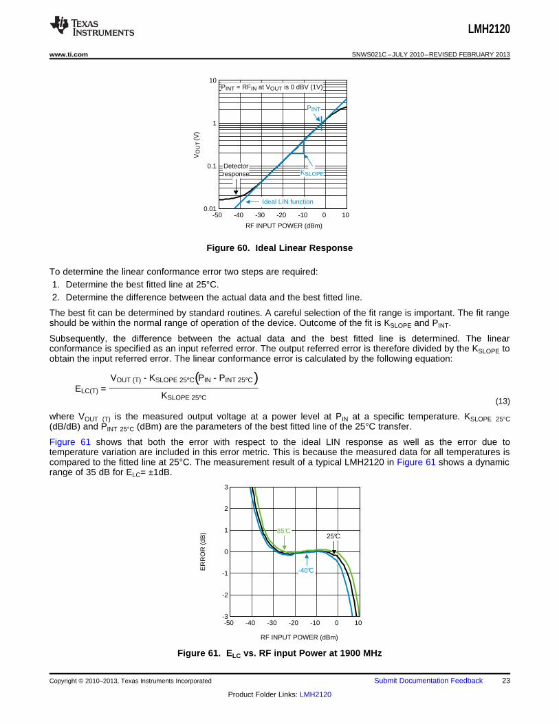
Linear Conformance error
The LMH2120 implements a linear detection function. In order to describe how close the transfer is to an ideallinear function the linear conformance error is used. To calculate the linear conformance error the detectortransfer function is modeled as a linear-in-V relationship between the input power and the output voltage.
The ideal linear-in-V transfer is modeled by 2 parameters:• Slope, KSLOPE
• Intercept, PINT
and is described by:VOUT = KSLOPE (PIN – PINT) (12)
where VOUT is the output voltage in dBV, KSLOPE is the slope of the function in dB/dB, PIN the input power level indBm and PINT is the power level in dBm at which the function intersects VOUT = 0 dBV = 1V (See Figure 60).
22 Submit Documentation Feedback Copyright © 2010–2013, Texas Instruments Incorporated
Product Folder Links: LMH2120
-50 -40 -30 -20 -10 0 10
3
2
1
0
-1
-2
-3
85°C
RF INPUT POWER (dBm)
ER
RO
R (
dB)
-40°C
25°C
ELC(T) = KSLOPE 25°C
VOUT (T) - KSLOPE 25°C PIN - PINT 25°C( )
RF INPUT POWER (dBm)
VO
UT
(V)
10
1
0.1
0.01-50 -40 -30 -20 -10 0 10
PINT
Detectorresponse KSLOPE
PINT = RFIN at VOUT is 0 dBV (1V)
Ideal LIN function
LMH2120
www.ti.com SNWS021C –JULY 2010–REVISED FEBRUARY 2013
Figure 60. Ideal Linear Response
To determine the linear conformance error two steps are required:1. Determine the best fitted line at 25°C.2. Determine the difference between the actual data and the best fitted line.
The best fit can be determined by standard routines. A careful selection of the fit range is important. The fit rangeshould be within the normal range of operation of the device. Outcome of the fit is KSLOPE and PINT.
Subsequently, the difference between the actual data and the best fitted line is determined. The linearconformance is specified as an input referred error. The output referred error is therefore divided by the KSLOPE toobtain the input referred error. The linear conformance error is calculated by the following equation:
(13)
where VOUT (T) is the measured output voltage at a power level at PIN at a specific temperature. KSLOPE 25°C(dB/dB) and PINT 25°C (dBm) are the parameters of the best fitted line of the 25°C transfer.
Figure 61 shows that both the error with respect to the ideal LIN response as well as the error due totemperature variation are included in this error metric. This is because the measured data for all temperatures iscompared to the fitted line at 25°C. The measurement result of a typical LMH2120 in Figure 61 shows a dynamicrange of 35 dB for ELC= ±1dB.
Figure 61. ELC vs. RF input Power at 1900 MHz
Copyright © 2010–2013, Texas Instruments Incorporated Submit Documentation Feedback 23
Product Folder Links: LMH2120
-50 -40 -30 -20 -10 0 10
2.0
1.5
1.0
0.5
0.0
-0.5
-1.0
-1.5
-2.0
RF INPUT POWER (dBm)
ER
RO
R (
dB)
-40°C
85°C
LMH2120
SNWS021C –JULY 2010–REVISED FEBRUARY 2013 www.ti.com
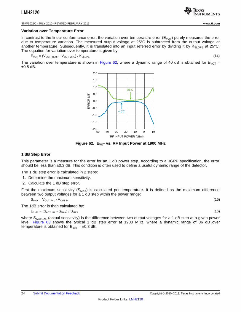
Variation over Temperature Error
In contrast to the linear conformance error, the variation over temperature error (EVOT) purely measures the errordue to temperature variation. The measured output voltage at 25°C is subtracted from the output voltage atanother temperature. Subsequently, it is translated into an input referred error by dividing it by KSLOPE at 25°C.The equation for variation over temperature is given by:
EVOT = (VOUT_TEMP - VOUT 25°C) / KSLOPE (14)
The variation over temperature is shown in Figure 62, where a dynamic range of 40 dB is obtained for EVOT =±0.5 dB.
Figure 62. EVOT vs. RF Input Power at 1900 MHz
1 dB Step Error
This parameter is a measure for the error for an 1 dB power step. According to a 3GPP specification, the errorshould be less than ±0.3 dB. This condition is often used to define a useful dynamic range of the detector.
The 1 dB step error is calculated in 2 steps:1. Determine the maximum sensitivity.2. Calculate the 1 dB step error.
First the maximum sensitivity (SMAX) is calculated per temperature. It is defined as the maximum differencebetween two output voltages for a 1 dB step within the power range:
SMAX = VOUT P+1 - VOUT P (15)
The 1dB error is than calculated by:E1 dB = (SACTUAL - SMAX) / SMAX (16)
where SACTUAL (actual sensitivity) is the difference between two output voltages for a 1 dB step at a given powerlevel. Figure 63 shows the typical 1 dB step error at 1900 MHz, where a dynamic range of 36 dB overtemperature is obtained for E1dB = ±0.3 dB.
24 Submit Documentation Feedback Copyright © 2010–2013, Texas Instruments Incorporated
Product Folder Links: LMH2120

P P+10 dB
PT PT+X
V2
V1
RFIN (dBm)
VO
UT (
dBV
)
25°C response
Temp (T)response
-50 -40 -30 -20 -10 0 10
1.5
1.2
0.9
0.6
0.3
0.0
-0.3
-0.6
-0.9
-1.2
-1.5
RF INPUT POWER (dBm)
ER
RO
R (
dB)
-40°C
85°C
25°C
LMH2120
www.ti.com SNWS021C –JULY 2010–REVISED FEBRUARY 2013
Figure 63. 1 dB Step Error vs. RF Input Power at 1900 MHz
10 dB step error
This error is defined in a different manner than the 1 dB step error. This parameter shows the input power errorover temperature for a 10 dB power step. The 10 dB step at 25°C is taken as a reference.
To determine the 10 dB step error first the output voltage levels (V1 and V2) for power levels “P” and “P+10dB”at the 25°C are determined (Figure 64). Subsequently these 2 output voltages are used to determine thecorresponding power levels at temperature T (PT and PT+X). The difference between those two power levelsminus 10 results in the 10 dB step error.
Figure 64. Graphical Representation of 10 dB Step Error Calculations
Figure 65 shows the typical 10 dB step error at 1900 MHz, where a dynamic range of 35 dB is obtained for E10dB= ±1dB.
Copyright © 2010–2013, Texas Instruments Incorporated Submit Documentation Feedback 25
Product Folder Links: LMH2120

RF INPUT POWER (dBm)
ER
RO
R (
dB)
1.5
1.0
0.5
0.0
-0.5
-1.0
-1.5-50 -40 -30 -20 -10 0 10
W-CDMA, REL8
W-CDMA, REL7
W-CDMA, REL6
-50 -40 -30 -20 -10 0
2.0
1.5
1.0
0.5
0.0
-0.5
-1.0
-1.5
-2.0
RF INPUT POWER (dBm)
ER
RO
R (
dB)
-40°C
85°C
LMH2120
SNWS021C –JULY 2010–REVISED FEBRUARY 2013 www.ti.com
Figure 65. 10 dB Step Error vs.RF Input Power at 1900 MHz
Variation due to Modulation
RMS power detectors, such as the LMH2120 are inherently insensitive to different modulation schemes. This incontrast to traditional detectors like peak detectors and LOG AMP detectors, where modulation forms with highpeak-to-average ratios (PAR) can cause significant output variation. This is because the measurement of thesedetectors is not an actual RMS measurement and is therefore waveform dependent.
To be able to compare the various detector types on modulation sensitivity, the variation due to modulationparameter is used. To calculate the variation due to modulation (EMOD), the measurement result for anunmodulated RF carrier is subtracted from the measurement result for a modulated RF carrier. The calculationsare similar to those for variation over temperature. The variation due to modulation can be calculated by:
EMOD = (VOUT_MOD - VOUT_CW) / KSLOPE (17)
where VOUT_MOD is the measured output voltage for an applied power level of a modulated signal, VOUT_CW is theoutput voltage as a result of an applied un-modulated signal having the same power level.
Figure 66 shows the variation due to modulation for W-CDMA, where a EMOD of 0.16 dB is obtained for adynamic range from -34 dBm to -2 dBm.
Figure 66. Variation due to Modulation for W-CDMA at 1900 MHz
26 Submit Documentation Feedback Copyright © 2010–2013, Texas Instruments Incorporated
Product Folder Links: LMH2120
-50 -40 -30 -20 -10 0 10
3
2
1
0
-1
-2
-3
125°C
RF INPUT POWER (dBm)
ER
RO
R (
dB)
-50°C
125°C
-50°C
In Steps of 25°C
-50 -40 -30 -20 -10 0 10
10
1
0.1
0.01
0.001
125°C
RF INPUT POWER (dBm)
VO
UT (
V)
-50°C
125°C
-50°C
In Steps of 25°C
LMH2120
www.ti.com SNWS021C –JULY 2010–REVISED FEBRUARY 2013
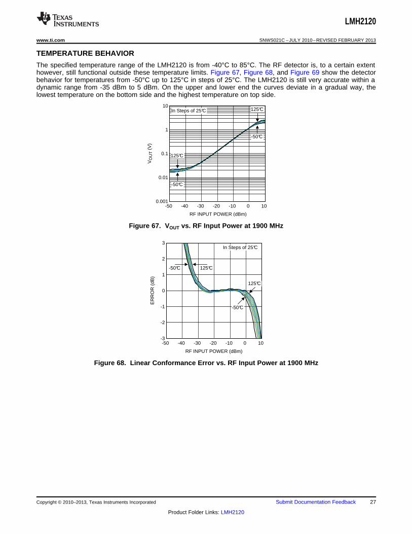
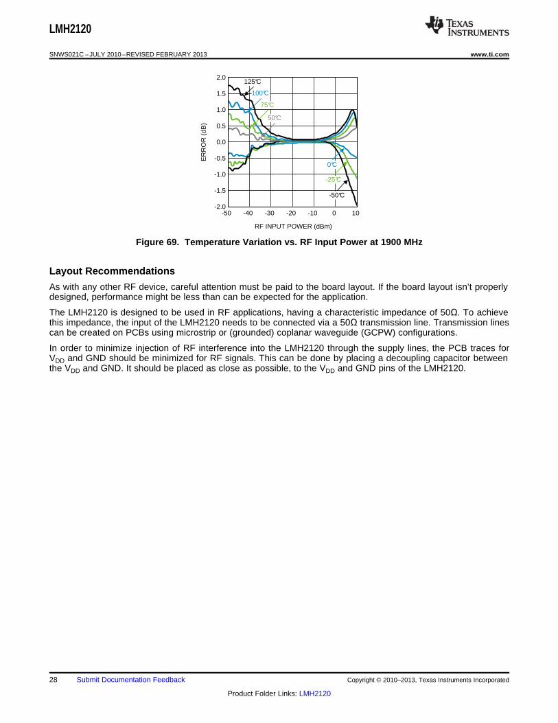
TEMPERATURE BEHAVIOR
The specified temperature range of the LMH2120 is from -40°C to 85°C. The RF detector is, to a certain extenthowever, still functional outside these temperature limits. Figure 67, Figure 68, and Figure 69 show the detectorbehavior for temperatures from -50°C up to 125°C in steps of 25°C. The LMH2120 is still very accurate within adynamic range from -35 dBm to 5 dBm. On the upper and lower end the curves deviate in a gradual way, thelowest temperature on the bottom side and the highest temperature on top side.
Figure 67. VOUT vs. RF Input Power at 1900 MHz
Figure 68. Linear Conformance Error vs. RF Input Power at 1900 MHz
Copyright © 2010–2013, Texas Instruments Incorporated Submit Documentation Feedback 27
Product Folder Links: LMH2120
-50 -40 -30 -20 -10 0 10
2.0
1.5
1.0
0.5
0.0
-0.5
-1.0
-1.5
-2.0
RF INPUT POWER (dBm)
ER
RO
R (
dB)
-50°C
0°C
-25°C
50°C
75°C
100°C
125°C
LMH2120
SNWS021C –JULY 2010–REVISED FEBRUARY 2013 www.ti.com
Figure 69. Temperature Variation vs. RF Input Power at 1900 MHz
Layout Recommendations
As with any other RF device, careful attention must be paid to the board layout. If the board layout isn’t properlydesigned, performance might be less than can be expected for the application.
The LMH2120 is designed to be used in RF applications, having a characteristic impedance of 50Ω. To achievethis impedance, the input of the LMH2120 needs to be connected via a 50Ω transmission line. Transmission linescan be created on PCBs using microstrip or (grounded) coplanar waveguide (GCPW) configurations.
In order to minimize injection of RF interference into the LMH2120 through the supply lines, the PCB traces forVDD and GND should be minimized for RF signals. This can be done by placing a decoupling capacitor betweenthe VDD and GND. It should be placed as close as possible, to the VDD and GND pins of the LMH2120.
28 Submit Documentation Feedback Copyright © 2010–2013, Texas Instruments Incorporated
Product Folder Links: LMH2120

LMH2120
www.ti.com SNWS021C –JULY 2010–REVISED FEBRUARY 2013
REVISION HISTORY
Changes from Revision B (February 2013) to Revision C Page
• Changed layout of National Data Sheet to TI format .......................................................................................................... 28
Copyright © 2010–2013, Texas Instruments Incorporated Submit Documentation Feedback 29
Product Folder Links: LMH2120

PACKAGE OPTION ADDENDUM
www.ti.com 10-Dec-2020
Addendum-Page 1
PACKAGING INFORMATION
Orderable Device Status(1)
Package Type PackageDrawing
Pins PackageQty
Eco Plan(2)
Lead finish/Ball material
(6)
MSL Peak Temp(3)
Op Temp (°C) Device Marking(4/5)
Samples
LMH2120UM/NOPB ACTIVE DSBGA YFZ 6 250 RoHS & Green SNAGCU Level-1-260C-UNLIM -40 to 85 R
LMH2120UMX/NOPB ACTIVE DSBGA YFZ 6 3000 RoHS & Green SNAGCU Level-1-260C-UNLIM -40 to 85 R
(1) The marketing status values are defined as follows:ACTIVE: Product device recommended for new designs.LIFEBUY: TI has announced that the device will be discontinued, and a lifetime-buy period is in effect.NRND: Not recommended for new designs. Device is in production to support existing customers, but TI does not recommend using this part in a new design.PREVIEW: Device has been announced but is not in production. Samples may or may not be available.OBSOLETE: TI has discontinued the production of the device.
(2) RoHS: TI defines "RoHS" to mean semiconductor products that are compliant with the current EU RoHS requirements for all 10 RoHS substances, including the requirement that RoHS substancedo not exceed 0.1% by weight in homogeneous materials. Where designed to be soldered at high temperatures, "RoHS" products are suitable for use in specified lead-free processes. TI mayreference these types of products as "Pb-Free".RoHS Exempt: TI defines "RoHS Exempt" to mean products that contain lead but are compliant with EU RoHS pursuant to a specific EU RoHS exemption.Green: TI defines "Green" to mean the content of Chlorine (Cl) and Bromine (Br) based flame retardants meet JS709B low halogen requirements of <=1000ppm threshold. Antimony trioxide basedflame retardants must also meet the <=1000ppm threshold requirement.
(3) MSL, Peak Temp. - The Moisture Sensitivity Level rating according to the JEDEC industry standard classifications, and peak solder temperature.
(4) There may be additional marking, which relates to the logo, the lot trace code information, or the environmental category on the device.
(5) Multiple Device Markings will be inside parentheses. Only one Device Marking contained in parentheses and separated by a "~" will appear on a device. If a line is indented then it is a continuationof the previous line and the two combined represent the entire Device Marking for that device.
(6) Lead finish/Ball material - Orderable Devices may have multiple material finish options. Finish options are separated by a vertical ruled line. Lead finish/Ball material values may wrap to twolines if the finish value exceeds the maximum column width.
Important Information and Disclaimer:The information provided on this page represents TI's knowledge and belief as of the date that it is provided. TI bases its knowledge and belief on informationprovided by third parties, and makes no representation or warranty as to the accuracy of such information. Efforts are underway to better integrate information from third parties. TI has taken andcontinues to take reasonable steps to provide representative and accurate information but may not have conducted destructive testing or chemical analysis on incoming materials and chemicals.TI and TI suppliers consider certain information to be proprietary, and thus CAS numbers and other limited information may not be available for release.
In no event shall TI's liability arising out of such information exceed the total purchase price of the TI part(s) at issue in this document sold by TI to Customer on an annual basis.

PACKAGE OPTION ADDENDUM
www.ti.com 10-Dec-2020
Addendum-Page 2
TAPE AND REEL INFORMATION
*All dimensions are nominal
Device PackageType
PackageDrawing
Pins SPQ ReelDiameter
(mm)
ReelWidth
W1 (mm)
A0(mm)
B0(mm)
K0(mm)
P1(mm)
W(mm)
Pin1Quadrant
LMH2120UM/NOPB DSBGA YFZ 6 250 178.0 8.4 0.89 1.3 0.56 4.0 8.0 Q1
LMH2120UMX/NOPB DSBGA YFZ 6 3000 178.0 8.4 0.89 1.3 0.56 4.0 8.0 Q1
PACKAGE MATERIALS INFORMATION
www.ti.com 14-Mar-2013
Pack Materials-Page 1
*All dimensions are nominal
Device Package Type Package Drawing Pins SPQ Length (mm) Width (mm) Height (mm)
LMH2120UM/NOPB DSBGA YFZ 6 250 210.0 185.0 35.0
LMH2120UMX/NOPB DSBGA YFZ 6 3000 210.0 185.0 35.0
PACKAGE MATERIALS INFORMATION
www.ti.com 14-Mar-2013
Pack Materials-Page 2
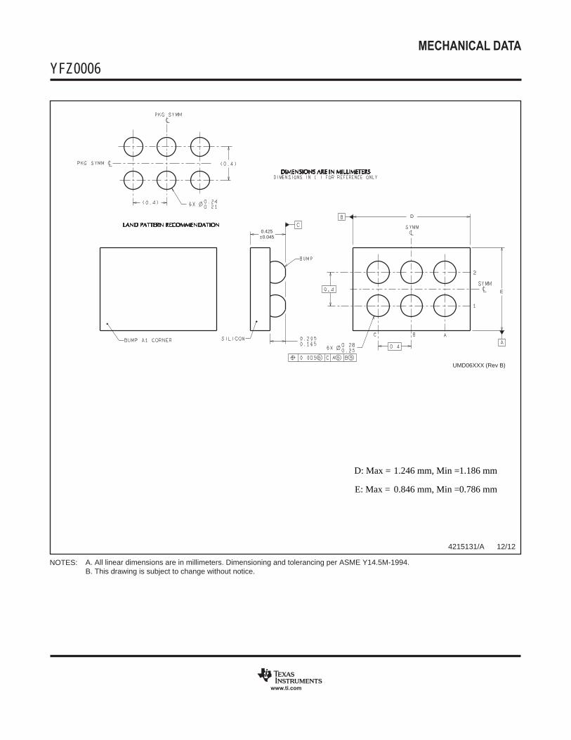
MECHANICAL DATA
YFZ0006xxx
www.ti.com
UMD06XXX (Rev B)
A. All linear dimensions are in millimeters. Dimensioning and tolerancing per ASME Y14.5M-1994.B. This drawing is subject to change without notice.
D
E
0.425±0.045
NOTES:
4215131/A 12/12
D: Max =
E: Max =
1.246 mm, Min =
0.846 mm, Min =
1.186 mm
0.786 mm

IMPORTANT NOTICE AND DISCLAIMERTI PROVIDES TECHNICAL AND RELIABILITY DATA (INCLUDING DATASHEETS), DESIGN RESOURCES (INCLUDING REFERENCEDESIGNS), APPLICATION OR OTHER DESIGN ADVICE, WEB TOOLS, SAFETY INFORMATION, AND OTHER RESOURCES “AS IS”AND WITH ALL FAULTS, AND DISCLAIMS ALL WARRANTIES, EXPRESS AND IMPLIED, INCLUDING WITHOUT LIMITATION ANYIMPLIED WARRANTIES OF MERCHANTABILITY, FITNESS FOR A PARTICULAR PURPOSE OR NON-INFRINGEMENT OF THIRDPARTY INTELLECTUAL PROPERTY RIGHTS.These resources are intended for skilled developers designing with TI products. You are solely responsible for (1) selecting the appropriateTI products for your application, (2) designing, validating and testing your application, and (3) ensuring your application meets applicablestandards, and any other safety, security, or other requirements. These resources are subject to change without notice. TI grants youpermission to use these resources only for development of an application that uses the TI products described in the resource. Otherreproduction and display of these resources is prohibited. No license is granted to any other TI intellectual property right or to any third partyintellectual property right. TI disclaims responsibility for, and you will fully indemnify TI and its representatives against, any claims, damages,costs, losses, and liabilities arising out of your use of these resources.TI’s products are provided subject to TI’s Terms of Sale (https:www.ti.com/legal/termsofsale.html) or other applicable terms available eitheron ti.com or provided in conjunction with such TI products. TI’s provision of these resources does not expand or otherwise alter TI’sapplicable warranties or warranty disclaimers for TI products.IMPORTANT NOTICE
Mailing Address: Texas Instruments, Post Office Box 655303, Dallas, Texas 75265Copyright © 2021, Texas Instruments Incorporated