LMF100 Dual High-Performance Switched Capacitor … Sheets/Texas Instruments PDFs... · LMF100 Dual...
40
Product Folder Sample & Buy Technical Documents Tools & Software Support & Community LMF100 SNOSBG9B – JULY 1999 – REVISED JUNE 2015 LMF100 Dual High-Performance Switched Capacitor Filters Not Recommended for New Designs 1 Features 3 Description The LMF100 device consists of two independent 1• Wide 4-V to 15-V Power Supply Range general-purpose, high-performance switched • Operation up to 100 kHz capacitor filters. With an external clock and two to • Low Offset Voltage: four resistors, each filter block can realize various second-order and first-order filtering functions. Each – Typically (50:1 or 100:1 mode): block has three outputs. One output can be – Vos1 = ±5 mV configured to perform either an allpass, highpass, or – Vos2 = ±15 mV notch function. The other two outputs perform bandpass and lowpass functions. The center – Vos3 = ±15 mV frequency of each filter stage is tuned by using an • Low Crosstalk: –60 dB external clock or a combination of a clock and resistor • Clock to Center Frequency Ratio Accuracy ±0.2% ratio. Up to a fourth-order biquadratic function can be (Typical) realized with one LMF100. Higher order filters are implemented by simply cascading additional • f 0 × Q Range up to 1.8 MHz packages, and all the classical filters (such as • Pin-Compatible With MF10 Butterworth, Bessel, Elliptic, and Chebyshev) can be realized. 2 Applications The LMF100 is fabricated on TI’s high-performance • Replacing Active RC Filters With Reduced Form analog silicon gate CMOS process, LMCMOS™. This Factors and Higher Accuracy and Tunability allows for the production of a very low-offset, high- • An Alternative to Integrated Continuous Time frequency filter building block. The LMF100 is pin- Filters compatible with the industry standard MF10, but provides greatly improved performance. Device Information (1) PART NUMBER PACKAGE BODY SIZE (NOM) SOIC (20) 12.60 mm × 10.00 mm LMF100 PDIP (20) 24.33 mm × 6.35 mm (1) For all available packages, see the orderable addendum at the end of the data sheet. Fourth-Order 100-kHz Butterworth Lowpass Filter Transfer Curve of Butterworth LP Filter Roll-Off Magnitude vs Frequency 1 An IMPORTANT NOTICE at the end of this data sheet addresses availability, warranty, changes, use in safety-critical applications, intellectual property matters and other important disclaimers. PRODUCTION DATA.
Transcript of LMF100 Dual High-Performance Switched Capacitor … Sheets/Texas Instruments PDFs... · LMF100 Dual...

Product
Folder
Sample &Buy
Technical
Documents
Tools &
Software
Support &Community
LMF100SNOSBG9B –JULY 1999–REVISED JUNE 2015
LMF100 Dual High-Performance Switched Capacitor FiltersNot Recommended for New Designs
1 Features 3 DescriptionThe LMF100 device consists of two independent
1• Wide 4-V to 15-V Power Supply Rangegeneral-purpose, high-performance switched• Operation up to 100 kHz capacitor filters. With an external clock and two to
• Low Offset Voltage: four resistors, each filter block can realize varioussecond-order and first-order filtering functions. Each– Typically (50:1 or 100:1 mode):block has three outputs. One output can be– Vos1 = ±5 mV configured to perform either an allpass, highpass, or
– Vos2 = ±15 mV notch function. The other two outputs performbandpass and lowpass functions. The center– Vos3 = ±15 mVfrequency of each filter stage is tuned by using an• Low Crosstalk: –60 dBexternal clock or a combination of a clock and resistor
• Clock to Center Frequency Ratio Accuracy ±0.2% ratio. Up to a fourth-order biquadratic function can be(Typical) realized with one LMF100. Higher order filters are
implemented by simply cascading additional• f0 × Q Range up to 1.8 MHzpackages, and all the classical filters (such as• Pin-Compatible With MF10Butterworth, Bessel, Elliptic, and Chebyshev) can berealized.2 ApplicationsThe LMF100 is fabricated on TI’s high-performance• Replacing Active RC Filters With Reduced Form analog silicon gate CMOS process, LMCMOS™. ThisFactors and Higher Accuracy and Tunability allows for the production of a very low-offset, high-
• An Alternative to Integrated Continuous Time frequency filter building block. The LMF100 is pin-Filters compatible with the industry standard MF10, but
provides greatly improved performance.
Device Information(1)
PART NUMBER PACKAGE BODY SIZE (NOM)SOIC (20) 12.60 mm × 10.00 mm
LMF100PDIP (20) 24.33 mm × 6.35 mm
(1) For all available packages, see the orderable addendum atthe end of the data sheet.
Fourth-Order 100-kHz Butterworth Lowpass Filter Transfer Curve of Butterworth LP Filter Roll-OffMagnitude vs Frequency
1
An IMPORTANT NOTICE at the end of this data sheet addresses availability, warranty, changes, use in safety-critical applications,intellectual property matters and other important disclaimers. PRODUCTION DATA.
Not Recommended for New Designs
LMF100SNOSBG9B –JULY 1999–REVISED JUNE 2015 www.ti.com
Table of Contents8.1 Overview ................................................................. 161 Features .................................................................. 18.2 Functional Block Diagram ....................................... 162 Applications ........................................................... 18.3 Feature Description................................................. 163 Description ............................................................. 18.4 Device Functional Modes........................................ 164 Revision History..................................................... 2
9 Application and Implementation ........................ 245 Pin Configuration and Functions ......................... 39.1 Application Information............................................ 246 Specifications......................................................... 49.2 Typical Application ................................................. 246.1 Absolute Maximum Ratings ...................................... 4
10 Power Supply Recommendations ..................... 326.2 ESD Ratings ............................................................ 411 Layout................................................................... 326.3 Recommended Operating Conditions....................... 4
11.1 Layout Guidelines ................................................. 326.4 Thermal Information ................................................. 512 Device and Documentation Support ................. 336.5 Electrical Characteristics for V+ = +5 V and V− = −5
V................................................................................. 5 12.1 Device Support .................................................... 336.6 Electrical Characteristics for V+ = +2.5 V and V− = 12.2 Community Resources.......................................... 33
−2.5 V......................................................................... 6 12.3 Trademarks ........................................................... 336.7 Logic Input Characteristics........................................ 8 12.4 Electrostatic Discharge Caution............................ 346.8 Typical Characteristics ............................................ 10 12.5 Glossary ................................................................ 34
7 Parameter Measurement Information ................ 14 13 Mechanical, Packaging, and Orderable7.1 Definition of Terms Graphics .................................. 14 Information ........................................................... 34
8 Detailed Description ............................................ 16
4 Revision History
Changes from Revision A (July 1999) to Revision B Page
• Added ESD Ratings table, Feature Description section, Device Functional Modes, Application and Implementationsection, Power Supply Recommendations section, Layout section, Device and Documentation Support section, andMechanical, Packaging, and Orderable Information section. ................................................................................................ 1
2 Submit Documentation Feedback Copyright © 1999–2015, Texas Instruments Incorporated
Product Folder Links: LMF100
Not Recommended for New Designs
LMF100www.ti.com SNOSBG9B –JULY 1999–REVISED JUNE 2015
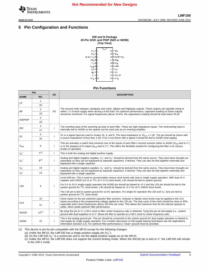
5 Pin Configuration and Functions
DW and N Package20-Pin SOIC and PDIP (N20 or M20B)
(Top View)
Pin FunctionsPIN
I/O DESCRIPTIONNAME NO.
1LP
20The second order lowpass, bandpass and notch, allpass and highpass outputs. These outputs can typically swing to2
BP I/O within 1 V of each supply when driving a 5-kΩ load. For optimum performance, capacitive loading on these outputs19 should be minimized. For signal frequencies above 15 kHz, the capacitance loading should be kept below 30 pF.3
N/AP/HP18
4 The inverting input of the summing op-amp of each filter. These are high impedance inputs. The noninverting input isINV I internally tied to AGND so the opamp can be used only as an inverting amplifier.17
5 S1 is a signal input pin used in modes 1b, 4, and 5. The input impedance is 1/fCLK x 1 pF. The pin should be driven withS1 I a source impedance of less than 1 kΩ. If S1 is not driven with a signal it should be tied to AGND (mid-supply).16
This pin activates a switch that connects one of the inputs of each filter’s second summer either to AGND (SA/B tied to V−)SA/B 6 I or to the lowpass (LP) output (SA/B tied to V+). This offers the flexibility needed for configuring the filter in its various
modes of operation.
7 (1) I This is both the analog and digital positive supply.VA+
Analog and digital negative supplies. VA– and VD
– should be derived from the same source. They have been brought out8 (1) IVD
+ separately so they can be bypassed by separate capacitors, if desired. They can also be tied together externally andbypassed with a single capacitor.
14VA– Analog and digital negative supplies. VA
– and VD– should be derived from the same source. They have been brought out
I separately so they can be bypassed by separate capacitors, if desired. They can also be tied together externally and13VD
– bypassed with a single capacitor.
Level shift pin. This is used to accommodate various clock levels with dual or single supply operation. With dual ±5-Vsupplies and CMOS (±5 V) or TTL (0 V–5 V) clock levels, LSh should be tied to system ground.
For 0-V to 10-V single-supply operation the AGND pin should be biased at +5 V and the LSh pin should be tied to theLSh 9 I system ground for TTL clock levels. LSh should be biased at +5 V for ±5-V CMOS clock levels.
The LSh pin is tied to system ground for ±2.5V operation. For single 5V operation the LSh and VD+ pins are tied to
system ground for TTL clock levels.
10 Clock inputs for the two switched capacitor filter sections. Unipolar or bipolar clock levels may be applied to the CLKinputs according to the programming voltage applied to the LSh pin. The duty cycle of the clock should be close to 50%,CLK I especially when clock frequencies above 200 kHz are used. This allows the maximum time for the internal opamps to11settle, which yields optimum filter performance.
By tying this pin to V+ a 50:1 clock to filter center frequency ratio is obtained. Tying this pin at mid-supply (i.e., system50/100 12 (1) I ground with dual supplies) or to V– allows the filter to operate at a 100:1 clock to center frequency ratio.
This is the analog ground pin. This pin should be connected to the system ground for dual supply operation or biased toAGND 15 I mid-supply for single-supply operation. For a further discussion of mid-supply biasing techniques see the Applications
Information (Section 3.2). For optimum filter performance a “clean” ground must be provided.
(1) This device is pin-for-pin compatible with the MF10 except for the following changes:(a) Unlike the MF10, the LMF100 has a single positive supply pin (VA
+).(b) On the LMF100 VD
+ is a control pin and is not the digital positive supply as on the MF10.(c) Unlike the MF10, the LMF100 does not support the current limiting mode. When the 50/100 pin is tied to V– the LMF100 will remain
in the 100:1 mode.
Copyright © 1999–2015, Texas Instruments Incorporated Submit Documentation Feedback 3
Product Folder Links: LMF100
Not Recommended for New Designs
LMF100SNOSBG9B –JULY 1999–REVISED JUNE 2015 www.ti.com
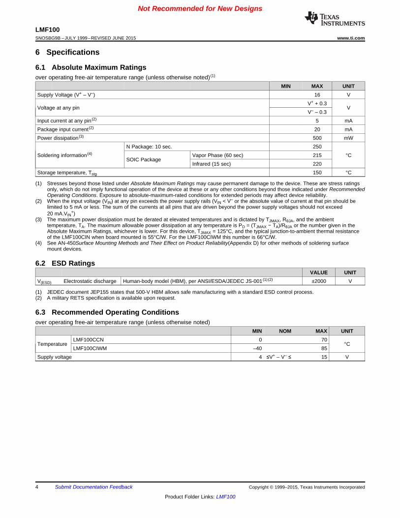
6 Specifications
6.1 Absolute Maximum Ratingsover operating free-air temperature range (unless otherwise noted) (1)
MIN MAX UNITSupply Voltage (V+ – V–) 16 V
V+ + 0.3Voltage at any pin V
V– – 0.3Input current at any pin (2) 5 mAPackage input current (2) 20 mAPower dissipation (3) 500 mW
N Package: 10 sec. 250Soldering information (4) Vapor Phase (60 sec) 215 °C
SOIC PackageInfrared (15 sec) 220
Storage temperature, Tstg 150 °C
(1) Stresses beyond those listed under Absolute Maximum Ratings may cause permanent damage to the device. These are stress ratingsonly, which do not imply functional operation of the device at these or any other conditions beyond those indicated under RecommendedOperating Conditions. Exposure to absolute-maximum-rated conditions for extended periods may affect device reliability.
(2) When the input voltage (VIN) at any pin exceeds the power supply rails (VIN < V– or the absolute value of current at that pin should belimited to 5 mA or less. The sum of the currents at all pins that are driven beyond the power supply voltages should not exceed20 mA.VIN
+)(3) The maximum power dissipation must be derated at elevated temperatures and is dictated by TJMAX, RθJA, and the ambient
temperature, TA. The maximum allowable power dissipation at any temperature is PD = (TJMAX − TA)/RθJA or the number given in theAbsolute Maximum Ratings, whichever is lower. For this device, TJMAX = 125°C, and the typical junction-to-ambient thermal resistanceof the LMF100CIN when board mounted is 55°C/W. For the LMF100CIWM this number is 66°C/W.
(4) See AN-450Surface Mounting Methods and Their Effect on Product Reliability(Appendix D) for other methods of soldering surfacemount devices.
6.2 ESD RatingsVALUE UNIT
V(ESD) Electrostatic discharge Human-body model (HBM), per ANSI/ESDA/JEDEC JS-001 (1) (2) ±2000 V
(1) JEDEC document JEP155 states that 500-V HBM allows safe manufacturing with a standard ESD control process.(2) A military RETS specification is available upon request.
6.3 Recommended Operating Conditionsover operating free-air temperature range (unless otherwise noted)
MIN NOM MAX UNITLMF100CCN 0 70
Temperature °CLMF100CIWM –40 85
Supply voltage 4 ≤V+ – V– ≤ 15 V
4 Submit Documentation Feedback Copyright © 1999–2015, Texas Instruments Incorporated
Product Folder Links: LMF100
Q
Q
D
Not Recommended for New Designs
LMF100www.ti.com SNOSBG9B –JULY 1999–REVISED JUNE 2015
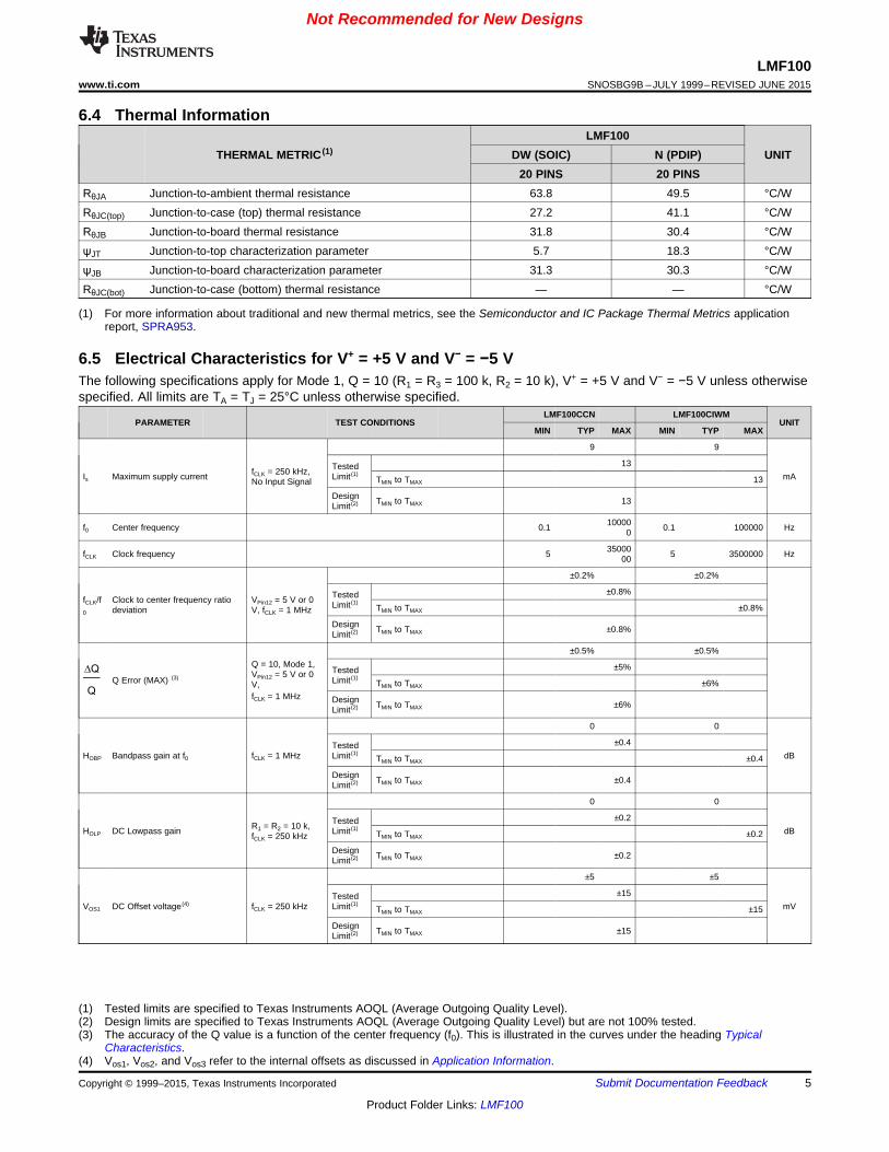
6.4 Thermal InformationLMF100
THERMAL METRIC (1) DW (SOIC) N (PDIP) UNIT20 PINS 20 PINS
RθJA Junction-to-ambient thermal resistance 63.8 49.5 °C/WRθJC(top) Junction-to-case (top) thermal resistance 27.2 41.1 °C/WRθJB Junction-to-board thermal resistance 31.8 30.4 °C/WψJT Junction-to-top characterization parameter 5.7 18.3 °C/WψJB Junction-to-board characterization parameter 31.3 30.3 °C/WRθJC(bot) Junction-to-case (bottom) thermal resistance — — °C/W
(1) For more information about traditional and new thermal metrics, see the Semiconductor and IC Package Thermal Metrics applicationreport, SPRA953.
6.5 Electrical Characteristics for V+ = +5 V and V− = −5 VThe following specifications apply for Mode 1, Q = 10 (R1 = R3 = 100 k, R2 = 10 k), V+ = +5 V and V− = −5 V unless otherwisespecified. All limits are TA = TJ = 25°C unless otherwise specified.
LMF100CCN LMF100CIWMPARAMETER TEST CONDITIONS UNIT
MIN TYP MAX MIN TYP MAX
9 9
13TestedfCLK = 250 kHz,Is Maximum supply current Limit (1) mATMIN to TMAX 13No Input SignalDesign TMIN to TMAX 13Limit (2)
10000f0 Center frequency 0.1 0.1 100000 Hz0
35000fCLK Clock frequency 5 5 3500000 Hz00
±0.2% ±0.2%
±0.8%TestedfCLK/f Clock to center frequency ratio VPin12 = 5 V or 0 Limit(1)TMIN to TMAX ±0.8%0 deviation V, fCLK = 1 MHz
Design TMIN to TMAX ±0.8%Limit(2)
±0.5% ±0.5%Q = 10, Mode 1, ±5%TestedVPin12 = 5 V or 0
Q Error (MAX) (3) Limit(1)TMIN to TMAX ±6%V,
fCLK = 1 MHz Design TMIN to TMAX ±6%Limit(2)
0 0
±0.4TestedHOBP Bandpass gain at f0 fCLK = 1 MHz Limit(1) dBTMIN to TMAX ±0.4
Design TMIN to TMAX ±0.4Limit(2)
0 0
±0.2TestedR1 = R2 = 10 k,HOLP DC Lowpass gain Limit(1) dBTMIN to TMAX ±0.2fCLK = 250 kHzDesign TMIN to TMAX ±0.2Limit(2)
±5 ±5
±15TestedVOS1 DC Offset voltage (4) fCLK = 250 kHz Limit(1) mVTMIN to TMAX ±15
Design TMIN to TMAX ±15Limit(2)
(1) Tested limits are specified to Texas Instruments AOQL (Average Outgoing Quality Level).(2) Design limits are specified to Texas Instruments AOQL (Average Outgoing Quality Level) but are not 100% tested.(3) The accuracy of the Q value is a function of the center frequency (f0). This is illustrated in the curves under the heading Typical
Characteristics.(4) Vos1, Vos2, and Vos3 refer to the internal offsets as discussed in Application Information.
Copyright © 1999–2015, Texas Instruments Incorporated Submit Documentation Feedback 5
Product Folder Links: LMF100

Not Recommended for New Designs
LMF100SNOSBG9B –JULY 1999–REVISED JUNE 2015 www.ti.com
Electrical Characteristics for V+ = +5 V and V− = −5 V (continued)The following specifications apply for Mode 1, Q = 10 (R1 = R3 = 100 k, R2 = 10 k), V+ = +5 V and V− = −5 V unless otherwisespecified. All limits are TA = TJ = 25°C unless otherwise specified.
LMF100CCN LMF100CIWMPARAMETER TEST CONDITIONS UNIT
MIN TYP MAX MIN TYP MAX
±30 ±30
±80Tested Limit (1) mVSA/B = V+
TMIN to TMAX ±80
Design Limit(2) TMIN to TMAX ±80VOS2 DC Offset voltage (4) fCLK = 250 kHz
±15 ±15
±70Tested Limit (1) mVSA/B = V–
TMIN to TMAX ±70
Design Limit(2) TMIN to TMAX ±70
±15 ±15
±40TestedVOS3 DC Offset voltage (4) fCLK = 250 kHz Limit(1) mVTMIN to TMAX ±60
Design TMIN to TMAX ±60Limit(2)
Crosstalk (5) A Side to B Side or B Side to A Side –60 –60 dB
fCLK = 250 kHz N 40 40
Output noise (6) 20 kHz Bandwidth BP 320 320 µV
100:1 Mode LP 300 300
Clock feedthrough (7) fCLK = 250 kHz 100:1 Mode 6 6 mV
4 4−4.7 −4.7
±3.8RL = 5 k Tested(All Outputs) Limit(1)
TMIN to TMAX ±3.7VOUT Minimum output voltage swing VDesign TMIN to TMAX ±3.7Limit(2)
RL = 3.5 k 3.9 3.9(All Outputs) −4.6 −4.6
GB Operational amplifier gain BW 5 5 MHzW product
SR Operational amplifier slew rate 20 20 V/µs
Source All Outputs 12 12 mAMaximum output,Isc Short circuit current (8)Sink All Outputs 45 45 mA
Tested Limit (1) 10Input current on Pins: 4, 5, 6, 9,IIN µA10, 11, 12, 16, 17 Design Limit(2) TMIN to TMAX 10
(5) Crosstalk between the internal filter sections is measured by applying a 1 VRMS 10-kHz signal to one bandpass filter section input andgrounding the input of the other bandpass filter section. The crosstalk is the ratio between the output of the grounded filter section andthe 1 VRMS input signal of the other section.
(6) In 50:1 mode the output noise is 3 dB higher.(7) In 50:1 mode the clock feed through is 6 dB higher.(8) The short circuit source current is measured by forcing the output that is being tested to its maximum positive voltage swing and then
shorting that output to the negative supply. The short circuit sink current is measured by forcing the output that is being tested to itsmaximum negative voltage swing and then shorting that output to the positive supply. These are the worst case conditions.
6.6 Electrical Characteristics for V+ = +2.5 V and V− = −2.5 VThe following specifications apply for Mode 1, Q = 10 (R1 = R3 = 100 k, R2 = 10 k), V+ = +2.50 V and V− = −2.50 V unlessotherwise specified. All limits are TA = TJ = 25°C unless otherwise specified.
LMF100CCN LMF100CIWMPARAMETER TEST CONDITIONS UNIT
MIN TYP MAX MIN TYP MAX
8 8
12 12TestedfCLK = 250 kHz,Is Maximum supply current Limit (1) mATMIN to TMAXNo Input SignalDesign 12Limit (2)
f0 Center frequency 0.1 50000 0.1 50000 Hz
(1) Tested limits are specified to Texas Instruments AOQL (Average Outgoing Quality Level).(2) Design limits are specified to Texas Instruments AOQL (Average Outgoing Quality Level) but are not 100% tested.
6 Submit Documentation Feedback Copyright © 1999–2015, Texas Instruments Incorporated
Product Folder Links: LMF100

Q
Q
D
Not Recommended for New Designs
LMF100www.ti.com SNOSBG9B –JULY 1999–REVISED JUNE 2015
Electrical Characteristics for V+ = +2.5 V and V− = −2.5 V (continued)The following specifications apply for Mode 1, Q = 10 (R1 = R3 = 100 k, R2 = 10 k), V+ = +2.50 V and V− = −2.50 V unlessotherwise specified. All limits are TA = TJ = 25°C unless otherwise specified.
LMF100CCN LMF100CIWMPARAMETER TEST CONDITIONS UNIT
MIN TYP MAX MIN TYP MAX
15000fCLK Clock frequency 5 5 1500000 Hz00
±0.2% ±0.2%
TestedfCLK/f Clock to center frequency ratio VPin12 = 5 V or 0 TMIN to TMAX ±1% ±1%Limit(1)
0 deviation V, fCLK = 1 MHzDesign ±1%Limit(2)
±0.5% ±0.5%Q = 10, Mode 1, ±5%TestedVPin12 = 5 V or 0
Q Error (MAX) (3) Limit(1)TMIN to TMAX ±8%V,
fCLK = 1 MHz Design TMIN to TMAX ±8%Limit(2)
0 0
±0.4TestedHOBP Bandpass gain at f0 fCLK = 1 MHz Limit(1) dBTMIN to TMAX ±0.5
Design TMIN to TMAX ±0.5Limit(2)
0 0
±0.2TestedR1 = R2 = 10 k,HOLP DC Lowpass gain Limit(1) dBTMIN to TMAX ±0.2fCLK = 250 kHzDesign TMIN to TMAX ±0.2Limit(2)
±5 ±5
±15 ±15TestedVOS1 DC Offset voltage (4) fCLK = 250 kHz Limit(1) mVTMIN to TMAX
Design TMIN to TMAX ±15Limit(2)
±20 ±20
±60Tested Limit (1) mVSA/B = V+
TMIN to TMAX ±60
Design Limit(2) TMIN to TMAX ±60VOS2 DC Offset voltage (4) fCLK = 250 kHz
±10 ±10 mV
±50Tested Limit (1)SA/B = V–
TMIN to TMAX ±60
Design Limit(2) TMIN to TMAX ±60
±10 ±10
±25TestedVOS3 DC Offset voltage (4) fCLK = 250 kHz Limit(1) mVTMIN to TMAX ±30
Design TMIN to TMAX ±30Limit(2)
Crosstalk (5) A Side to B Side or B Side to A Side –65 –65 dB
fCLK = 250 kHz N 25 25
Output noise (6) 20 kHz Bandwidth BP 250 250 µV
100:1 Mode LP 220 220
Clock feedthrough (7) fCLK = 250 kHz 100:1 Mode 2 2 mV
(3) The accuracy of the Q value is a function of the center frequency (f0). This is illustrated in the curves under the heading TypicalCharacteristics.
(4) Vos1, Vos2, and Vos3 refer to the internal offsets as discussed in the Application Information.(5) Crosstalk between the internal filter sections is measured by applying a 1 VRMS 10-kHz signal to one bandpass filter section input and
grounding the input of the other bandpass filter section. The crosstalk is the ratio between the output of the grounded filter section andthe 1 VRMS input signal of the other section.
(6) In 50:1 mode the output noise is 3 dB higher.(7) In 50:1 mode the clock feed through is 6 dB higher.
Copyright © 1999–2015, Texas Instruments Incorporated Submit Documentation Feedback 7
Product Folder Links: LMF100

Not Recommended for New Designs
LMF100SNOSBG9B –JULY 1999–REVISED JUNE 2015 www.ti.com
Electrical Characteristics for V+ = +2.5 V and V− = −2.5 V (continued)The following specifications apply for Mode 1, Q = 10 (R1 = R3 = 100 k, R2 = 10 k), V+ = +2.50 V and V− = −2.50 V unlessotherwise specified. All limits are TA = TJ = 25°C unless otherwise specified.
LMF100CCN LMF100CIWMPARAMETER TEST CONDITIONS UNIT
MIN TYP MAX MIN TYP MAX
RL = 5 k 1.6 1.6All Outputs −2.2 −2.2
±1.5Tested VLimit(1)RL = 5 k (All TMIN to TMAX ±1.4
VOUT Minimum output voltage swing Outputs)Design TMIN to TMAX ±1.4Limit(2)
1.5 1.5RL = 3.5 k VAll Outputs −2.1 −2.1
GB Operational amplifier gain BW 5 5 MHzW product
SR Operational amplifier slew rate 18 18 V/µs
Source All Outputs 10 10 mAMaximum output,Isc Short circuit current (8)Sink All Outputs 20 20 mA
(8) The short circuit source current is measured by forcing the output that is being tested to its maximum positive voltage swing and thenshorting that output to the negative supply. The short circuit sink current is measured by forcing the output that is being tested to itsmaximum negative voltage swing and then shorting that output to the positive supply. These are the worst case conditions.
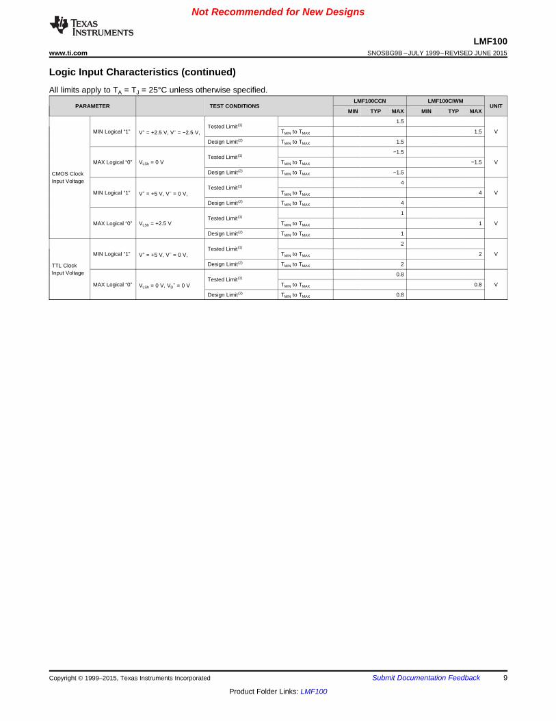
6.7 Logic Input CharacteristicsAll limits apply to TA = TJ = 25°C unless otherwise specified.
LMF100CCN LMF100CIWMPARAMETER TEST CONDITIONS UNIT
MIN TYP MAX MIN TYP MAX
3Tested Limit (1)
MIN Logical “1” TMIN to TMAX 3 VV+ = +5 V, V− = −5 V,
Design Limit (2) TMIN to TMAX 3
−3Tested Limit (1)
MAX Logical “0” VLSh = 0 V TMIN to TMAX –3 V
Design Limit(2) TMIN to TMAX −3CMOS ClockInput Voltage 8
Tested Limit (1)
MIN Logical “1” TMIN to TMAX 8 VV+ = +10 V, V− = 0 V,
Design Limit(2) TMIN to TMAX 8
2Tested Limit (1)
MAX Logical “0” VLSh = +5 V TMIN to TMAX 2 V
Design Limit(2) TMIN to TMAX 2
2Tested Limit (1)
MIN Logical “1” TMIN to TMAX 2 VV+ = +5 V, V− = −5 V,
Design Limit(2) TMIN to TMAX 2
0.8Tested Limit (1)
MAX Logical “0” VLSh = 0 V TMIN to TMAX 0.8 V
Design Limit(2) TMIN to TMAX 0.8TTL ClockInput Voltage 2
Tested Limit (1)
MIN Logical “1” TMIN to TMAX 2 VV+ = +10 V, V− = 0 V,
Design Limit(2) TMIN to TMAX 2
0.8Tested Limit (1)
MAX Logical “0” VLSh = 0 V TMIN to TMAX 0.8 V
Design Limit(2) TMIN to TMAX 0.8
(1) Tested limits are specified to Texas Instruments AOQL (Average Outgoing Quality Level).(2) Design limits are specified to Texas Instruments AOQL (Average Outgoing Quality Level) but are not 100% tested.
8 Submit Documentation Feedback Copyright © 1999–2015, Texas Instruments Incorporated
Product Folder Links: LMF100
Not Recommended for New Designs
LMF100www.ti.com SNOSBG9B –JULY 1999–REVISED JUNE 2015
Logic Input Characteristics (continued)All limits apply to TA = TJ = 25°C unless otherwise specified.
LMF100CCN LMF100CIWMPARAMETER TEST CONDITIONS UNIT
MIN TYP MAX MIN TYP MAX
1.5Tested Limit (1)
MIN Logical “1” TMIN to TMAX 1.5 VV+ = +2.5 V, V− = −2.5 V,
Design Limit(2) TMIN to TMAX 1.5
−1.5Tested Limit (1)
MAX Logical “0” VLSh = 0 V TMIN to TMAX −1.5 V
Design Limit(2) TMIN to TMAX −1.5CMOS ClockInput Voltage 4
Tested Limit (1)
MIN Logical “1” TMIN to TMAX 4 VV+ = +5 V, V− = 0 V,
Design Limit(2) TMIN to TMAX 4
1Tested Limit (1)
MAX Logical “0” VLSh = +2.5 V TMIN to TMAX 1 V
Design Limit(2) TMIN to TMAX 1
2Tested Limit (1)
MIN Logical “1” TMIN to TMAX 2 VV+ = +5 V, V− = 0 V,
Design Limit(2) TMIN to TMAX 2TTL ClockInput Voltage 0.8
Tested Limit (1)
MAX Logical “0” TMIN to TMAX 0.8 VVLSh = 0 V, VD+ = 0 V
Design Limit(2) TMIN to TMAX 0.8
Copyright © 1999–2015, Texas Instruments Incorporated Submit Documentation Feedback 9
Product Folder Links: LMF100

Not Recommended for New Designs
LMF100SNOSBG9B –JULY 1999–REVISED JUNE 2015 www.ti.com
6.8 Typical Characteristics
Figure 1. Power Supply Current vs Power Supply Voltage Figure 2. Power Supply Current vs Temperature
Figure 4. Positive Output Swing vs TemperatureFigure 3. Output Swing vs Supply Voltage
Figure 5. Negative Output Swing vs Temperature Figure 6. Positive Output Voltage Swing vs Load Resistance
10 Submit Documentation Feedback Copyright © 1999–2015, Texas Instruments Incorporated
Product Folder Links: LMF100
Not Recommended for New Designs
LMF100www.ti.com SNOSBG9B –JULY 1999–REVISED JUNE 2015
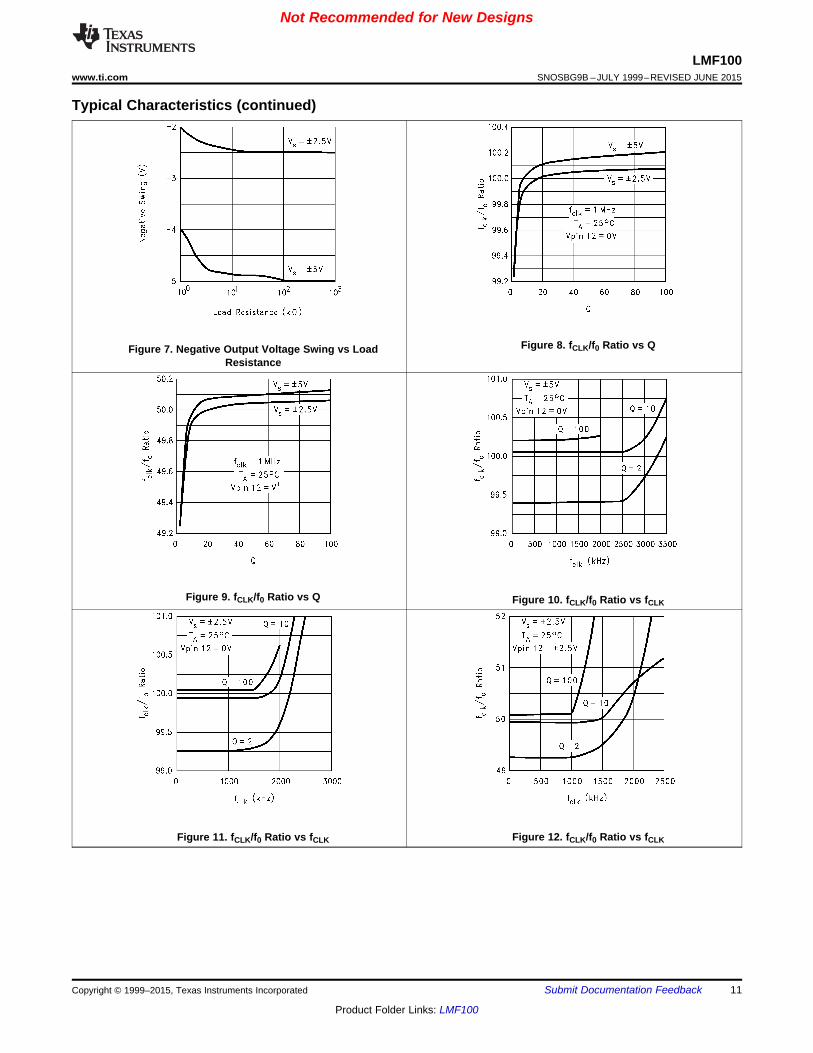
Typical Characteristics (continued)
Figure 8. fCLK/f0 Ratio vs QFigure 7. Negative Output Voltage Swing vs LoadResistance
Figure 9. fCLK/f0 Ratio vs Q Figure 10. fCLK/f0 Ratio vs fCLK
Figure 12. fCLK/f0 Ratio vs fCLKFigure 11. fCLK/f0 Ratio vs fCLK
Copyright © 1999–2015, Texas Instruments Incorporated Submit Documentation Feedback 11
Product Folder Links: LMF100

Not Recommended for New Designs
LMF100SNOSBG9B –JULY 1999–REVISED JUNE 2015 www.ti.com
Typical Characteristics (continued)
Figure 14. fCLK/f0 Ratio vs TemperatureFigure 13. fCLK/f0 Ratio vs fCLK
Figure 15. fCLK/f0 Ratio vs Temperature Figure 16. Q Deviation vs Clock Frequency
Figure 17. Q Deviation vs Clock Frequency Figure 18. Q Deviation vs Clock Frequency
12 Submit Documentation Feedback Copyright © 1999–2015, Texas Instruments Incorporated
Product Folder Links: LMF100

Not Recommended for New Designs
LMF100www.ti.com SNOSBG9B –JULY 1999–REVISED JUNE 2015
Typical Characteristics (continued)
Figure 20. Q Deviation vs TemperatureFigure 19. Q Deviation vs Clock Frequency
Figure 22. Maximum f0 vs Q at Vs = ±7.5 VFigure 21. Q Deviation vs Temperature
Figure 23. Maximum f0 vs Q at Vs = ±5 V Figure 24. Maximum f0 vs Q at Vs = ±2.5 V
Copyright © 1999–2015, Texas Instruments Incorporated Submit Documentation Feedback 13
Product Folder Links: LMF100

Not Recommended for New Designs
LMF100SNOSBG9B –JULY 1999–REVISED JUNE 2015 www.ti.com
7 Parameter Measurement Information
7.1 Definition of Terms Graphics
Figure 25. Second-Order Bandpass Response Gain Figure 26. Second-Order Bandpass ResponsePhase
Figure 27. Second-Order Lowpass Response Gain Figure 28. Second-Order Lowpass ResponsePhase
Figure 29. Second-Order Highpass Response Gain Figure 30. Second-Order Highpass ResponsePhase
Figure 31. Second-Order Notch Response Gain Figure 32. Second-Order Notch Response Phase
Figure 33. Second-Order Allpass Response Gain Figure 34. Second-Order Allpass Response Phase
14 Submit Documentation Feedback Copyright © 1999–2015, Texas Instruments Incorporated
Product Folder Links: LMF100

Not Recommended for New Designs
LMF100www.ti.com SNOSBG9B –JULY 1999–REVISED JUNE 2015
Definition of Terms Graphics (continued)
Figure 35. Bandpass Response of Various Second-Order Figure 36. Lowpass Response of Various Second-OrderFilters as a Function of Q. Filters as a Function of Q.
Gains and Center Frequencies are Normalized to Unity Gains and Center Frequencies are Normalized to UnityGain Phase
Figure 37. Highpass Response of Various Second-Order Figure 38. Notch Response of Various Second-OrderFilters as a Function of Q. Filters as a Function of Q.
Gains and Center Frequencies are Normalized to Unity Gains and Center Frequencies are Normalized to UnityGain Gain
Figure 39. Allpass Response of Various Second-Order Filters as a Function of Q.Gains and Center Frequencies are Normalized to Unity Gain
Copyright © 1999–2015, Texas Instruments Incorporated Submit Documentation Feedback 15
Product Folder Links: LMF100
Not Recommended for New Designs
LMF100SNOSBG9B –JULY 1999–REVISED JUNE 2015 www.ti.com
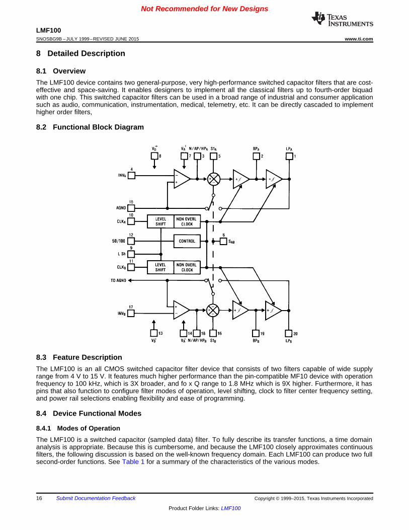
8 Detailed Description
8.1 OverviewThe LMF100 device contains two general-purpose, very high-performance switched capacitor filters that are cost-effective and space-saving. It enables designers to implement all the classical filters up to fourth-order biquadwith one chip. This switched capacitor filters can be used in a broad range of industrial and consumer applicationsuch as audio, communication, instrumentation, medical, telemetry, etc. It can be directly cascaded to implementhigher order filters,
8.2 Functional Block Diagram
8.3 Feature DescriptionThe LMF100 is an all CMOS switched capacitor filter device that consists of two filters capable of wide supplyrange from 4 V to 15 V. It features much higher performance than the pin-compatible MF10 device with operationfrequency to 100 kHz, which is 3X broader, and fo x Q range to 1.8 MHz which is 9X higher. Furthermore, it haspins that also function to configure filter modes of operation, level shifting, clock to filter center frequency setting,and power rail selections enabling flexibility and ease of programming.
8.4 Device Functional Modes
8.4.1 Modes of OperationThe LMF100 is a switched capacitor (sampled data) filter. To fully describe its transfer functions, a time domainanalysis is appropriate. Because this is cumbersome, and because the LMF100 closely approximates continuousfilters, the following discussion is based on the well-known frequency domain. Each LMF100 can produce two fullsecond-order functions. See Table 1 for a summary of the characteristics of the various modes.
16 Submit Documentation Feedback Copyright © 1999–2015, Texas Instruments Incorporated
Product Folder Links: LMF100

1OBPCircuit dynamics : H Q=
2OBPH 1(noninverting)=
1OBP
R3H
R2= -
OLP OLP(peak) OLPH 1; H Q H (for high Q's)= - @ ´
CLK CLK0
f ff or
100 50=
OLP(peak) OLPH Q H (for high Q's)@ ´
OBPOLP OBP OLP ON
HH or H H Q H Q
Q= = ´ = ´
1OBPCircuit dynamics : H Q=
BW the 3 dB bandwidth of the bandpass output.= -
0f R3Q quality factor of the complex pole pair
BW R2= = =
ONH Notch output gain as=
f 0®
CLKf f / 2®
2
1
R
R
-
=
OBP
R3H Bandpass gain (at f 0)
R1= ® = -
OLP
R2H Lowpass gain (as f 0)
R1= ® = -
notch 0f center frequency of the imaginary zero pair f= =
CLK CLK0
f ff center frequency of the complex pole pair or
100 50= =
Not Recommended for New Designs
LMF100www.ti.com SNOSBG9B –JULY 1999–REVISED JUNE 2015
Device Functional Modes (continued)8.4.1.1 MODE 1: Notch 1, Bandpass, Lowpass Outputs:
fnotch = f0 (See Figure 40)
(1)
(2)
(3)
(4)
(5)
(6)
(7)
(8)
(9)
(10)
8.4.1.2 MODE 1a: Noninverting BP, LP (See Figure 41)
(11)
(12)
(13)
(14)
(15)
(16)
Note: VIN should be driven from a low-impedance (<1 kΩ) source.
Figure 40. MODE 1 Figure 41. MODE 1a
Copyright © 1999–2015, Texas Instruments Incorporated Submit Documentation Feedback 17
Product Folder Links: LMF100

2 1 2OBP OLP ON OLP ONFilter dynamics : H Q H H H H= =
1
CLKON
fH Notch output gain as f R2 / R1
2
æ ö= ® = -ç ÷
è ø
1ON
R2 / R1H Notch output gain (as f 0)
R2 / R4 1= ® = -
+
OBP 0H Bandpass gain (at f f ) R3 / R1= ® = -
OLP
R2 / R1H Lowpass output gain (as f 0)
R2 / R4 1= ® = -
+
R2 / R4 1Q quality factor of the complex pole pair
R2 / R3
+= =
CLK CLKnotch
f ff or
100 50=
CLK CLK0
f fR2 R2f center frequency 1 or 1
100 R4 50 R4= = ´ + ´ +
OLP(peak) OLPH Q H (for high Q's)@ ´
ONOBP
H QH
2
´
=
OBPOLP OBP OLP
HH or H H Q 2
2Q= = ´ =
BW the 3 dB bandwidth of the bandpass output.= -
0f R3Q quality factor of the complex pole pair
BW R2= = =
ONH Notch output gain as=
f 0®
CLKf f / 2®
2
1
R
R
-
=
OBP
R3H Bandpass gain (at f 0)
R1= ® = -
OLP
R2H Lowpass gain (as f 0)
R1= ® = -
notch 0f center frequency of the imaginary zero pair f= =
CLK CLK0
f ff center frequency of the complex pole pair 2 or 2
100 50= = ´ ´
Not Recommended for New Designs
LMF100SNOSBG9B –JULY 1999–REVISED JUNE 2015 www.ti.com
Device Functional Modes (continued)8.4.1.3 MODE 1b: Notch 1, Bandpass, Lowpass Outputs:
fnotch = f0 (See Figure 42)
(17)
(18)
(19)
(20)
(21)
(22)
(23)
Circuit dynamics:
(24)
(25)
(26)
8.4.1.4 MODE 2: Notch 2, Bandpass, Lowpass: fnotch < f0 (See Figure 43)
(27)
(28)
(29)
(30)
(31)
(32)
(33)
(34)
18 Submit Documentation Feedback Copyright © 1999–2015, Texas Instruments Incorporated
Product Folder Links: LMF100
CLK CLKh hn
l l
f fR Rf notch frequency or
100 R 50 R= =
OLP
R4H
R1= -
OBP
R3H
R1= -
OHP
R2H
R1= -
R2 R3Q
R4 R2= ´
CLK CLK0
f fR2 R2f or
100 R4 50 R4= ´ ´
OHP(peak) OHPH Q H (for high Q's)@ ´
OLP(peak) OLPH Q H (for high Q's)@ ´
OHPOBP OHP OLP
OLP
HR2Circuit dynamics : ; H H H Q
R4 H= = ´ ´
OLP
R4H Lowpass gain (as f 0)
R1= ® = -
( )OBP 0
R3H Bandpass gain as f f
R1= ® = -
CLKOLP
f R2H Highpass gain at f
2 R1
æ ö= ® = -ç ÷
è ø
R2 R3Q quality factor of the complex pole pair
R4 R2= = ´
CLK CLK0
f fR2 R2f 1 or
100 R4 50 R4= ´ + ´
Not Recommended for New Designs
LMF100www.ti.com SNOSBG9B –JULY 1999–REVISED JUNE 2015
Device Functional Modes (continued)
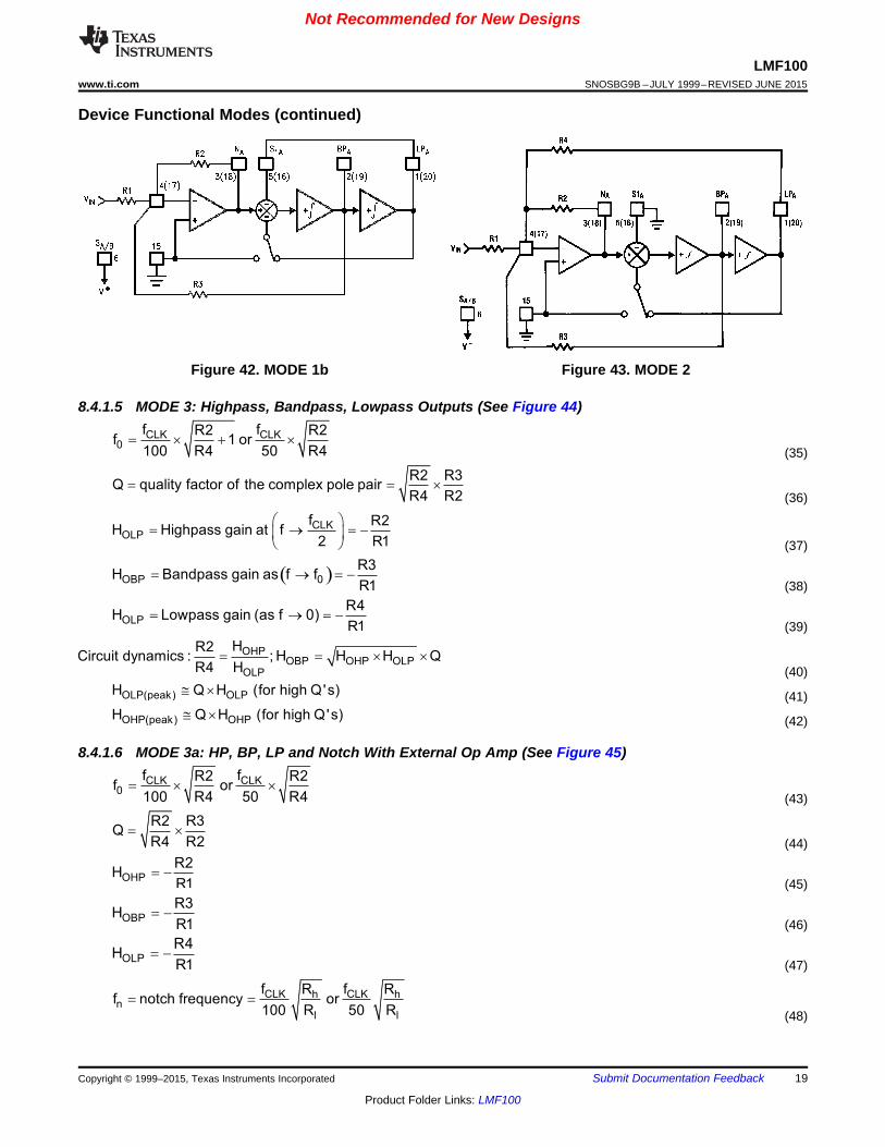
Figure 42. MODE 1b Figure 43. MODE 2
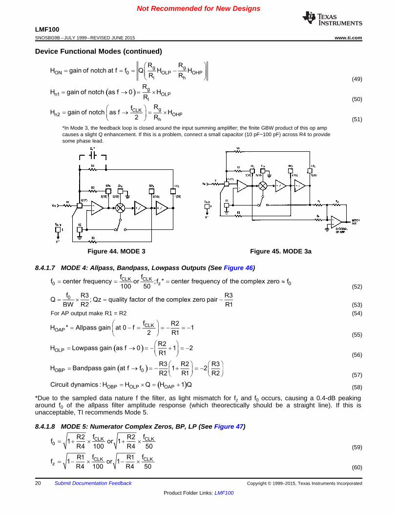
8.4.1.5 MODE 3: Highpass, Bandpass, Lowpass Outputs (See Figure 44)
(35)
(36)
(37)
(38)
(39)
(40)
(41)
(42)
8.4.1.6 MODE 3a: HP, BP, LP and Notch With External Op Amp (See Figure 45)
(43)
(44)
(45)
(46)
(47)
(48)
Copyright © 1999–2015, Texas Instruments Incorporated Submit Documentation Feedback 19
Product Folder Links: LMF100
CLK CLKz
f fR1 R1f 1 or 1
R4 100 R4 50= - ´ - ´
CLK CLK0
f fR2 R2f 1 or 1
R4 100 R4 50= + ´ + ´
( )OBP OLP OAPCircuit dynamics : H H Q H 1 Q= ´ = +
( )OBP 0
R3 R2 R3H Bandpass gain at f f 1 2
R2 R1 R2
æ ö æ ö= ® = - + = -ç ÷ ç ÷
è ø è ø
( )OLP
R2H Lowpass gain as f 0 1 2
R1
æ ö= ® = - + = -ç ÷
è ø
CLKOAP
f R2H * Allpass gain at 0 f 1
2 R1
æ ö= - = = - = -ç ÷
è ø
0f R3 R3Q ; Qz quality factor of the complex zero pair
BW R2 R1= ´ = -
CLK CLK0 z 0
f ff center frequency or ;f * center frequency of the complex zero f
100 50= = = »
gCLKn2 OHP
h
RfH gain of notch as f H
2 R
æ ö= ® = ´ç ÷
è ø
( ) gn1 OLP
l
RH gain of notch as f 0 H
R= ® = ´
g gON 0 OLP OHP
l h
R RH gain of notch at f f Q H H
R R
æ ö= = = -ç ÷ç ÷
è ø
Not Recommended for New Designs
LMF100SNOSBG9B –JULY 1999–REVISED JUNE 2015 www.ti.com
Device Functional Modes (continued)
(49)
(50)
(51)*In Mode 3, the feedback loop is closed around the input summing amplifier; the finite GBW product of this op ampcauses a slight Q enhancement. If this is a problem, connect a small capacitor (10 pF−100 pF) across R4 to providesome phase lead.
Figure 44. MODE 3 Figure 45. MODE 3a
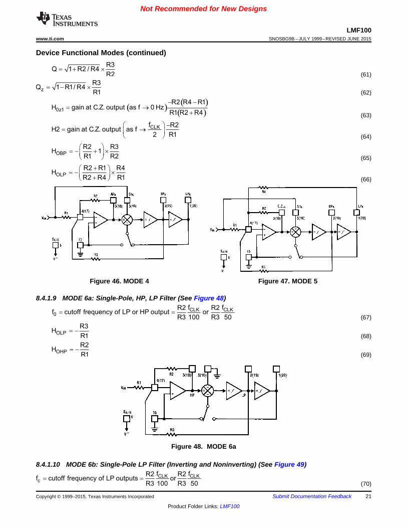
8.4.1.7 MODE 4: Allpass, Bandpass, Lowpass Outputs (See Figure 46)
(52)
(53)For AP output make R1 = R2 (54)
(55)
(56)
(57)
(58)
*Due to the sampled data nature f the filter, as light mismatch for fz and f0 occurs, causing a 0.4-dB peakingaround f0 of the allpass filter amplitude response (which theorectically should be a straight line). If this isunacceptable, TI recommends Mode 5.
8.4.1.8 MODE 5: Numerator Complex Zeros, BP, LP (See Figure 47)
(59)
(60)
20 Submit Documentation Feedback Copyright © 1999–2015, Texas Instruments Incorporated
Product Folder Links: LMF100
CLK CLKc
f fR2 R2f cutoff frequency of LP outputs or
R3 100 R3 50= =
OHP
R2H
R1= -
OLP
R3H
R1= -
CLK CLK0
f fR2 R2f cutoff frequency of LP or HP output or
R3 100 R3 50= =
OLP
R2 R1 R4H
R2 R4 R1
+æ ö= - ´ç ÷+è ø
OBP
R2 R3H 1
R1 R2
æ ö= - + ´ç ÷
è ø
CLKf R2H2 gain at C.Z. output as f
2 R1
æ ö -= ®ç ÷
è ø
( )( )
( )0z1
R2 R4 R1H gain at C.Z. output as f 0 Hz
R1 R2 R4
- -= ®
+
z
R3Q 1 R1/ R4
R1= - ´
R3Q 1 R2 / R4
R2= + ´
Not Recommended for New Designs
LMF100www.ti.com SNOSBG9B –JULY 1999–REVISED JUNE 2015
Device Functional Modes (continued)
(61)
(62)
(63)
(64)
(65)
(66)
Figure 46. MODE 4 Figure 47. MODE 5
8.4.1.9 MODE 6a: Single-Pole, HP, LP Filter (See Figure 48)
(67)
(68)
(69)
Figure 48. MODE 6a
8.4.1.10 MODE 6b: Single-Pole LP Filter (Inverting and Noninverting) (See Figure 49)
(70)
Copyright © 1999–2015, Texas Instruments Incorporated Submit Documentation Feedback 21
Product Folder Links: LMF100

CLK CLK
16 8int egrator time constant or
f ft = @
1 2 3R R R= =
OLPH 2= -
OAP CLKH 1(as f f / 2)= - ®
OAPH 1(as f 0)= ®
CLK CLKc
f ff or
100 50=
2OHP
R3H
R2=
( )1OLPH 1 noninverting=
Not Recommended for New Designs
LMF100SNOSBG9B –JULY 1999–REVISED JUNE 2015 www.ti.com
Device Functional Modes (continued)
(71)
(72)
8.4.1.11 MODE 6c: Single-Pole, AP, LP Filter (See Figure 50)
(73)
(74)
(75)
(76)
(77)
Figure 49. MODE 6b Figure 50. MODE 6c
8.4.1.12 Summing Integrator (See Figure 52)
Figure 51. Equivalent Circuit
Figure 52. MODE 7
22 Submit Documentation Feedback Copyright © 1999–2015, Texas Instruments Incorporated
Product Folder Links: LMF100

OLP1
OLP2
H 1
R3H
R2
= +
-
=
Not Recommended for New Designs
LMF100www.ti.com SNOSBG9B –JULY 1999–REVISED JUNE 2015
Device Functional Modes (continued)Table 1. Summary of Modes (1)
NUMBERADJUSTABLEOFMODE BP LP HP N AP NOTESRESISTOR fCLK/f0
S
1 * * * 3 No
HOBP1 = −Q1a HOLP = + 1 2 No May need input buffer. Poor dynamics for high Q.HOBP2 = + 1
1b * * * 3 No Useful for high-frequency applications.
Yes (above fCLK/50 or2 * * * 3 fCLK/100)
Universal State-Variable Filter. Best general-purpose3 * * * 4 Yes mode.
3a * * * * 7 Yes As above, but also includes resistor-tuneable notch.
Gives Allpass response with HOAP = − 1 and HOLP =4 * * * 3 No −2.
Gives flatter allpass response than above5 * * * 4 Yes if R1 = R2 = 0.02R4.
6a * * 3 Yes Single pole.
6b 2 Yes Single pole.
6c * * 3 No Single pole.
7 2 Yes Summing integrator with adjustable time constant.
(1) Realizable filter types (that is, lowpass) denoted by asterisks (*). Unless otherwise noted, gains of various filter outputs are inverting andadjustable by resistor ratios.
Copyright © 1999–2015, Texas Instruments Incorporated Submit Documentation Feedback 23
Product Folder Links: LMF100
Not Recommended for New Designs
LMF100SNOSBG9B –JULY 1999–REVISED JUNE 2015 www.ti.com
9 Application and Implementation
NOTEInformation in the following applications sections is not part of the TI componentspecification, and TI does not warrant its accuracy or completeness. TI’s customers areresponsible for determining suitability of components for their purposes. Customers shouldvalidate and test their design implementation to confirm system functionality.
9.1 Application InformationThe LMF100 is a general purpose dual second-order state variable filter whose center frequency is proportionalto the frequency of the square wave applied to the clock input (fCLK). The various clocking options aresummarized in Table 2.
Table 2. Clocking OptionsPOWER SUPPLY CLOCK LEVELS LSh VD
+
−5 V and +5 V TTL (0 V to 5 V) 0 V +5 V−5 V and +5 V CMOS (−5 V to +5 V) 0 V +5 V0 V and 10 V TTL (0 V to 5 V) 0 V +10 V0 V and 10 V CMOS (0 V to 10 V) +5 V +10 V−2.5 V and +2.5 V CMOS 0 V +2.5 V0 V and 5 V (−2.5 V to +2.5 V) TTL (0 V to 5 V) 0 V 0 V0 V and 5 V CMOS (0 V to 5 V) +2.5 V +5 V
By connecting pin 12 to the appropriate DC voltage, the filter center frequency, f0, can be made equal to eitherfCLK/100 or fCLK/50. f0 can be very accurately set (within ±0.6%) by using a crystal clock oscillator, or can beeasily varied over a wide frequency range by adjusting the clock frequency. If desired, the fCLK/f0 ratio can bealtered by external resistors as in Figure 43 through Figure 49. This is useful when high-order filters (greater thantwo) are to be realized by cascading the second-order sections. This allows each stage to be stagger tuned whileusing only one clock. The filter Q and gain are set by external resistor ratios.
All of the five second-order filter types can be built using either section of the LMF100. These are illustrated inFigure 25 through Figure 33 along with their transfer functions and some related equations. Figure 35 shows theeffect of Q on the shapes of these curves.
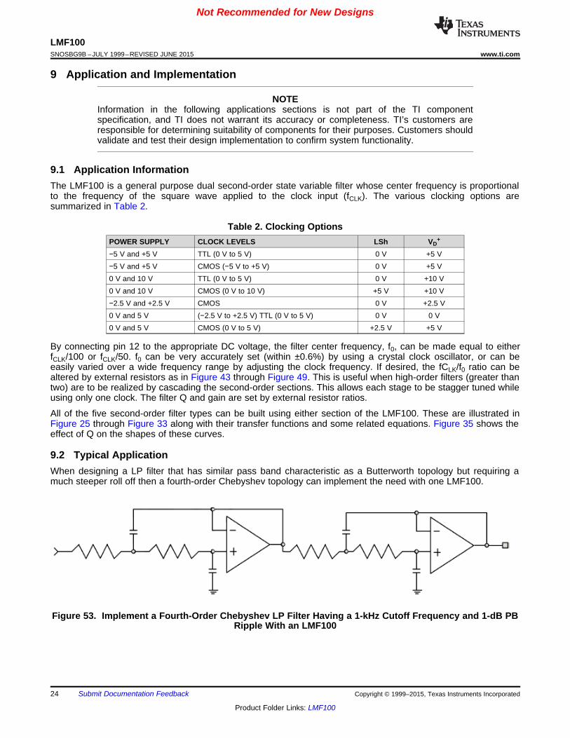
9.2 Typical ApplicationWhen designing a LP filter that has similar pass band characteristic as a Butterworth topology but requiring amuch steeper roll off then a fourth-order Chebyshev topology can implement the need with one LMF100.
Figure 53. Implement a Fourth-Order Chebyshev LP Filter Having a 1-kHz Cutoff Frequency and 1-dB PBRipple With an LMF100
24 Submit Documentation Feedback Copyright © 1999–2015, Texas Instruments Incorporated
Product Folder Links: LMF100
( )
1B
4B 1B
2 20B
2B 4B 2 2CLK
4 43B B 2B 4B
R 20k
R R 20k
f (993)R R 20k 19.7k
(1000)f / 100
R Q R R 3.559 1.97 10 2 10 70.6k
=
= =
= = =
= = ´ ´ ´ =
( )
2 240A
2A 4A 2 2CLK
3 43A A 2A 4A
f (529)R R 2 10 5.6k and
(1000)f / 100
R Q R R 0.785 5.6 10 2 10 8.3k
= = ´ ´ =
= = ´ ´ ´ =
CLK
0
f
f
Not Recommended for New Designs
LMF100www.ti.com SNOSBG9B –JULY 1999–REVISED JUNE 2015
Typical Application (continued)9.2.1 Design RequirementsIn order to design a filter using the LMF100, we must define the necessary values of three parameters for eachsecond-order section: f0, the filter section’s center frequency; H0, the passband gain; and the filter’s Q. These aredetermined by the characteristics required of the filter being designed.
As an example, assume that a system requires a fourth-order Chebyshev lowpass filter with 1-dB ripple, unitygain at DC, and 1000 Hz cutoff frequency. As the system order is four, it is realizable using both second-ordersections of an LMF100. Many filter design texts (and TI Switched Capacitor Filter Handbook) include tables thatlist the characteristics (f0 and Q) of each of the second-order filter sections needed to synthesize a given higher-order filter. For the Chebyshev filter defined above, such a table yields the following characteristics:
f0A = 529 Hz — — QA = 0.785f0B = 993 Hz — — QB = 3.559
For unity gain at DC, we also specify:
H0A = 1H0B = 1
The desired clock-to-cutoff-frequency ratio for the overall filter of this example is 100, and a 100-kHz clock signalis available. The required center frequencies for the two second-order sections will not be obtainable with clock-
to-center-frequency ratios of 50 or 100. It will be necessary to adjust externally. From Table 1, we see thatMode 3 can be used to produce a lowpass filter with resistor-adjustable center frequency.
In most filter designs involving multiple second-order stages, it is best to place the stages with lower Q valuesahead of stages with higher Q, especially when the higher Q is greater than 0.707. This is due to the higherrelative gain at the center frequency of a higher-Q stage. Placing a stage with lower Q ahead of a higher-Q stagewill provide some attenuation at the center frequency and thus help avoid clipping of signals near this frequency.For this example, stage A has the lower Q (0.785) so it will be placed ahead of the other stage.
For the first section, we begin the design by choosing a convenient value for the input resistance: R1A = 20 k.The absolute value of the passband gain HOLPA is made equal to 1 by choosing R4A such that: R4A = −HOLPAR1A =R1A = 20 k. If the 50/100/CL pin is connected to mid-supply for nominal 100:1 clock-to-center-frequency ratio, wefind R2A by:
The resistors for the second section are found in a similar fashion:
Copyright © 1999–2015, Texas Instruments Incorporated Submit Documentation Feedback 25
Product Folder Links: LMF100
Not Recommended for New Designs
LMF100SNOSBG9B –JULY 1999–REVISED JUNE 2015 www.ti.com
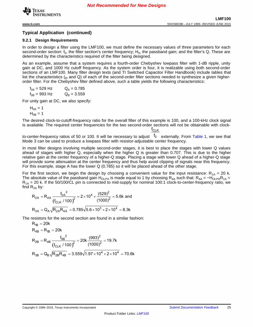
Typical Application (continued)The complete circuit is shown in Figure 54 for split ±5-V power supplies. TI highly recommends Supply bypasscapacitors.
±5-V power supply. 0-V to 5-V TTL or ±5-V CMOS logic levels.
Figure 54. Fourth-Order Chebyshev Lowpass Filter from Example in 3.1.
9.2.2 Detailed Design Procedure
9.2.2.1 Single-Supply OperationThe LMF100 can also operate with a single-ended power supply. Figure 55 shows the example filter with asingle-ended power supply. VA
+ and VD+ are again connected to the positive power supply (4 to 15 volts), and
VA− and VD
− are connected to ground. The AGND pin must be tied to V+/2 for single-supply operation. This half-supply point should be very “clean”, as any noise appearing on it will be treated as an input to the filter. It can bederived from the supply voltage with a pair of resistors and a bypass capacitor (Figure 56), or a low-impedancehalf-supply voltage can be made using a three-terminal voltage regulator or an operational amplifier (Figure 57and Figure 58). The passive resistor divider with a bypass capacitor is sufficient for many applications, providedthat the time constant is long enough to reject any power supply noise. It is also important that the half-supplyreference present a low impedance to the clock frequency, so at very low clock frequencies the regulator oroperational amplifier approaches may be preferable because they will require smaller capacitors to filter the clockfrequency. The main power supply voltage should be clean (preferably regulated) and bypassed with 0.1 μF
26 Submit Documentation Feedback Copyright © 1999–2015, Texas Instruments Incorporated
Product Folder Links: LMF100

Not Recommended for New Designs
LMF100www.ti.com SNOSBG9B –JULY 1999–REVISED JUNE 2015
Typical Application (continued)
Single 10-V power supply. 0-V to 5-V TTL logic levels. Input signals should be referred to half-supply or appliedthrough a coupling capacitor.
Figure 55. Fourth-Order Chebyshev Lowpass Filter from Example in 3.1.
Figure 56. Three Ways of Generating V+/2 for Figure 57. Three Ways of Generating V+/2 forSingle-Supply Operation Option A Single-Supply Operation Option B
Figure 58. Three Ways of Generating V+/2 for Single-Supply Operation Option C
9.2.2.2 Dynamic ConsiderationsThe maximum signal handling capability of the LMF100, like that of any active filter, is limited by the powersupply voltages used. The amplifiers in the LMF100 can swing to within about 1 volt of the supplies, so the inputsignals must be kept small enough that none of the outputs will exceed these limits. If the LMF100 is operatingon ±5 volts, for example, the outputs will clip at about 8 Vp-p. The maximum input voltage multiplied by the filtergain should therefore be less than 8 Vp-p.
Copyright © 1999–2015, Texas Instruments Incorporated Submit Documentation Feedback 27
Product Folder Links: LMF100

OS3OS(N) OS3 OS2 p
OS(BP) OS3
OS(LP) OS(N) OS2
VR2 1 1V 1 V V : R R1|| R3 || R4
Rp 1 R2 / R4 1 R4 / R2 Q 1 R2 / R4
V V
V V V
æ ö= + ´ + - =ç ÷
+ + +è ø
=
= -
OS(N) OS1 OS3
OS(BP) OS3
OS(N) OS2OS(LP)
R2 R2 R2V V 1 V
R3 R1 R3
V V
V VV
2 2
æ ö= + + -ç ÷
è ø
=
= -
OS3OS OS1
OS OS3
OS OS OS2
V1V (N.INV.BP) 1 V
Q Q
V (INV.BP) V
V (LP) V (N.INV.BP) V
æ ö= + -ç ÷
è ø
=
= -
OS3OS(N) OS1 OLP
OS(BP) OS3
OS(LP) OS(N) OS2
V1V V 1 H
Q Q
V V
V V V
æ ö= + + -ç ÷
è ø
=
= -
Not Recommended for New Designs
LMF100SNOSBG9B –JULY 1999–REVISED JUNE 2015 www.ti.com
Typical Application (continued)If the filter Q is high, the gain at the lowpass or highpass outputs will be much greater than the nominal filter gain(Figure 35). As an example, a lowpass filter with a Q of 10 will have a 20-dB peak in its amplitude response at f0.If the nominal gain of the filter (HOLP) is equal to 1, the gain at f0 will be 10. The maximum input signal at f0 musttherefore be less than 800 mVp-p when the circuit is operated on ±5 volt supplies.
Also, one output can have a reasonable small voltage on it while another is saturated. This is most likely for acircuit such as the notch in Mode 1 (Figure 40). The notch output will be very small at f0, so it might appear safeto apply a large signal to the input. However, the bandpass will have its maximum gain at f0 and can clip ifoverdriven. If one output clips, the performance at the other outputs will be degraded, so avoid overdriving anyfilter section, even ones whose outputs are not being directly used. Accompanying Figure 40 through Figure 50are equations labeled circuit dynamics, which relate the Q and the gains at the various outputs. These should beconsulted to determine peak circuit gains and maximum allowable signals for a given application.
9.2.2.3 Offset VoltageThe switched capacitor integrators of the LMF100 have a slightly higher input offset voltage than found in atypical continuous time active filter integrator. Because of TI's new LMCMOS process and new design techniquesthe internal offsets have been minimized, compared to the industry standard MF10. Figure 59 shows anequivalent circuit of the LMF100 from which the output DC offsets can be calculated. Typical values for theseoffsets with SA/B tied to V+ are:
VOS1 = opamp offset = ±5 mVVOS2 = ±30 mV at 50:1 or 100:1VOS3 = ±15 mV at 50:1 or 100:1
When SA/B is tied to V−, VOS2 will approximately halve. The DC offset at the BP output is equal to the input offsetof the lowpass integrator (VOS3). The offsets at the other outputs depend on the mode of operation and theresistor ratios, as described in the following expressions.
Mode 1 and Mode 4
Mode 1a
Mode 1b
Mode 2 and Mode 5
28 Submit Documentation Feedback Copyright © 1999–2015, Texas Instruments Incorporated
Product Folder Links: LMF100

OS(LP(N.INV)) OS2
3 3OS(LP(INV)) OS1 OS2
2 2
V V
R RV V 1 V
R R
=
æ ö= + -ç ÷
è ø
OS(HP) OS2
3 3 3OS(LP) OS1 OS2
2 1 2
V V
R R RV V 1 V
R R R
=
æ ö= + + -ç ÷
è ø
OS(HP) OS2
OS(BP) OS3
OS(LP) OS1 OS2 OS3p
p
V V
V V
R4 R4 R4V V 1 V V
R R2 R3
R R1|| R2 || R3
=
=
é ù æ ö æ ö= + - -ê ú ç ÷ ç ÷
è ø è øê úë û
=
Not Recommended for New Designs
LMF100www.ti.com SNOSBG9B –JULY 1999–REVISED JUNE 2015
Typical Application (continued)Mode 3
Mode 6a and 6c
Mode 6b
Figure 59. Offset Voltage Sources
In many applications, the outputs are AC-coupled and DC offsets are not bothersome unless large signals areapplied to the filter input. However, larger offset voltages will cause clipping to occur at lower AC signal levels,and clipping at any of the outputs will cause gain nonlinearities and will change f0 and Q. When operating inMode 3, offsets can become excessively large if R2 and R4 are used to make fCLK/f0 significantly higher than thenominal value, especially if Q is also high.
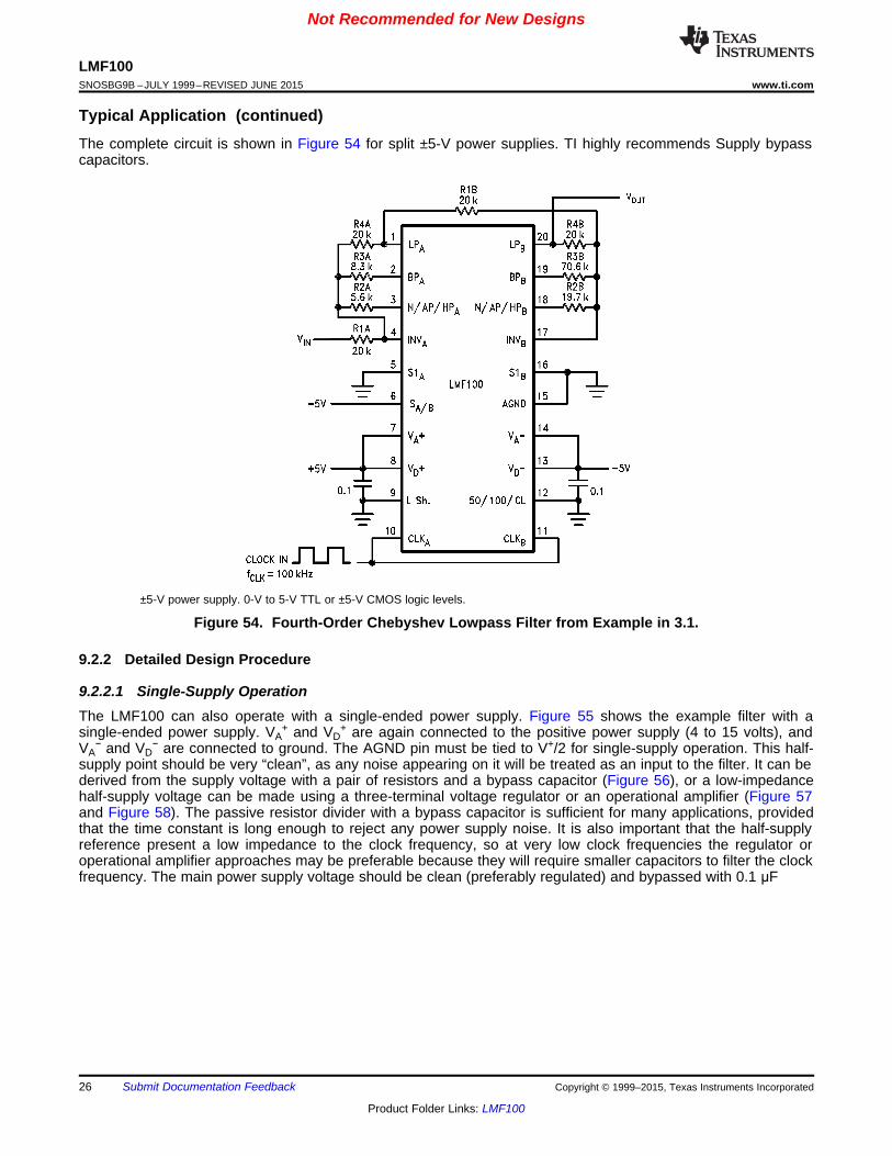
For example, Figure 60 shows a second-order 60-Hz notch filter. This circuit yields a notch with about 40 dB ofattenuation at 60 Hz. A notch is formed by subtracting the bandpass output of a mode 3 configuration from theinput using the unused side B operational amplifier. The Q is 10 and the gain is 1 V/V in the passband. However,fCLK/f0 = 1000 to allow for a wide input spectrum. This means that for pin 12 tied to ground (100:1 mode),R4/R2 = 100. The offset voltage at the lowpass output (LP) will be about 3 V. However, this is an extreme caseand the resistor ratio is usually much smaller. Where necessary, the offset voltage can be adjusted by using thecircuit of Figure 61. This allows adjustment of VOS1, which will have varying effects on the different outputs asdescribed in the above equations. Some outputs cannot be adjusted this way in some modes, however (VOS(BP)in modes 1a and 3, for example).
Copyright © 1999–2015, Texas Instruments Incorporated Submit Documentation Feedback 29
Product Folder Links: LMF100
Not Recommended for New Designs
LMF100SNOSBG9B –JULY 1999–REVISED JUNE 2015 www.ti.com
Typical Application (continued)
Figure 60. Second-Order Notch Filter
Figure 61. Method for Trimming VOS
9.2.2.4 Sampled Data System ConsiderationsThe LMF100 is a sampled data filter, and as such, differs in many ways from conventional continuous-time filters.An important characteristic of sampled-data systems is their effect on signals at frequencies greater than one-half the sampling frequency. (The sampling frequency of the LMF100 is the same as its clock frequency.) If asignal with a frequency greater than one-half the sampling frequency is applied to the input of a sampled datasystem, it will be reflected to a frequency less than one-half the sampling frequency. Thus, an input signal whose
30 Submit Documentation Feedback Copyright © 1999–2015, Texas Instruments Incorporated
Product Folder Links: LMF100
Not Recommended for New Designs
LMF100www.ti.com SNOSBG9B –JULY 1999–REVISED JUNE 2015
Typical Application (continued)frequency is fs/2 + 100 Hz will cause the system to respond as though the input frequency was fs/2 − 100 Hz.This phenomenon is known as aliasing, and can be reduced or eliminated by limiting the input signal spectrum toless than fs/2. This may in some cases require the use of a bandwidth-limiting filter ahead of the LMF100 to limitthe input spectrum. However, because the clock frequency is much higher than the center frequency, this willoften not be necessary.
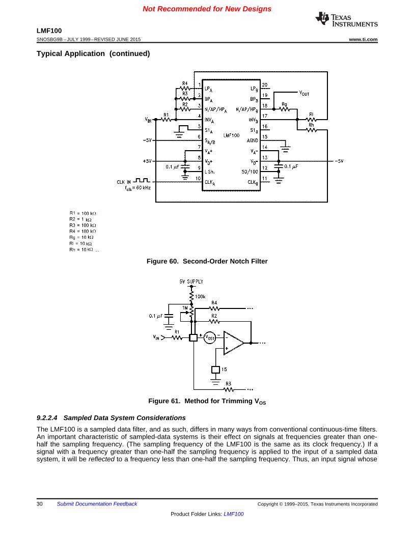
Another characteristic of sampled-data circuits is that the output signal changes amplitude once every samplingperiod, resulting in “steps” in the output voltage which occur at the clock rate (Figure 62). If necessary, these canbe “smoothed” with a simple R-C lowpass filter at the LMF100 output.
The ratio of fCLK to fc (normally either 50:1 or 100:1) will also affect performance. A ratio of 100:1 will reduce anyaliasing problems and is usually recommended for wideband input signals. In noise-sensitive applications, a ratioof 100:1 will result in 3 dB lower output noise for the same filter configuration.
The accuracy of the fCLK/f0 ratio is dependent on the value of Q. This is shown in the curves under the headingFigure 54. As Q is changed, the true value of the ratio changes as well. Unless the Q is low, the error in fCLK/f0will be small. If the error is too large for a specific application, use a mode that allows adjustment of the ratio withexternal resistors.
Figure 62. The Sampled-Data Output Waveform
9.2.3 Application Curve
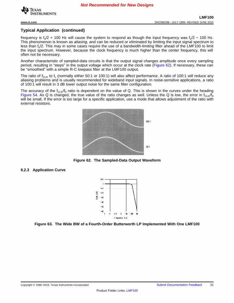
Figure 63. The Wide BW of a Fourth-Order Butterworth LP Implemented With One LMF100
Copyright © 1999–2015, Texas Instruments Incorporated Submit Documentation Feedback 31
Product Folder Links: LMF100

Not Recommended for New Designs
LMF100SNOSBG9B –JULY 1999–REVISED JUNE 2015 www.ti.com
10 Power Supply RecommendationsThe LMF100 can operate with a single-ended power supply as well as bipolar supplies. Refer to Figure 56through Figure 58 for methods of generating V+/2 for single-supply operation. In this circumstance, pins VA+ andVD+ are connected to the positive power supply (4 to 15 V), and VA− and VD− are connected to ground. TheAGND pin must be tied to V+/2. Furthermore, the half-supply node should be very “clean”, as any noiseappearing on it will be treated as an input to the filter. Ensure liberal bypassing is employed to reject any supplynoise and present a low impedance to the clock frequency. Bypass caps should always be located as close tothe supply pins a practical. Moreover, the regulator or op-amp approaches of generating V+/e is preferred forvery low clock frequency applications. The main power supply voltage should also be clean (preferablyregulated) and bypassed with 0.1-µF nonpolar ceramic capacitor. If there is no bulk cap nearby, a 10-uFelectrolytic tantalum in parallel with the 0.1-µF supply bypass cap should achieve cleaner and optimal transientresponse. Select capacitors with low ESR and ESL rating and test them to ensure no ringing occurs. The powersource is preferably a linear supply or regulator. If a switching supply is used ensure it is a clean switcher anddeploy proper bypassing or post regulate with an LDO as necessary.
11 Layout
11.1 Layout GuidelinesThe most critical part to the success of a switched capacitor filter design is a properly layout PCB. Because ofthe mixed signal circuitry involved, take extra care in the board design for noise abatement, star-grounding, andshielding techniques. A ground plane must separate digital and analog ground planes if possible, or haveseparate paths and join together only at the common return node at the supply source. All component leads andPCB tracks are kept as short as possible. The filter clock input should be a shielded cable.
32 Submit Documentation Feedback Copyright © 1999–2015, Texas Instruments Incorporated
Product Folder Links: LMF100
22 o o
OAPz
AP2 2o
o
sH s
QH (s)
ss
Q
æ öw + w-ç ÷
ç ÷è ø=
w- + w
Not Recommended for New Designs
LMF100www.ti.com SNOSBG9B –JULY 1999–REVISED JUNE 2015
12 Device and Documentation Support
12.1 Device Support
12.1.1 Device Nomenclature
12.1.1.1 Definitions of TermsfCLK: the frequency of the external clock signal applied to pin 10 or 11.
f0: center frequency of the second order function complex pole pair. f0 is measured at the bandpass outputs ofthe LMF100, and is the frequency of maximum bandpass gain. (Figure 25).
fnotch: the frequency of minimum (ideally zero) gain at the notch outputs.
fz: the center frequency of the second order complex zero pair, if any. If fz is different from f0 and if Qz is high, itcan be observed as the frequency of a notch at the allpass output. (Figure 46).
Q: “quality factor” of the 2nd order filter. Q is measured at the bandpass outputs of the LMF100 and is equal to f0divided by the −3 dB bandwidth of the 2nd order bandpass filter (Figure 25). The value of Q determines the shapeof the 2nd order filter responses as shown in Figure 35.
Qz: the quality factor of the second order complex zero pair, if any. QZ is related to the allpass characteristic,which is written:
where QZ = Q for an allpass response.
HOLP: the gain (in V/V) of the lowpass output as f → 0 Hz (Figure 27).
HOHP: the gain (in V/V) of the highpass output as f → fCLK/2 (Figure 29).
HON: the gain (in V/V) of the notch output as f → 0 Hz and as f → fCLK/2, when the notch filter has equal gainabove and below the center frequency (Figure 31 ). When the low-frequency gain differs from the high-frequencygain, as in modes 2 and 3a (Figure 43 and Figure 45), the two quantities below are used in place of HON.
HON1: the gain (in V/V) of the notch output as f → 0 Hz.
HON2: the gain (in V/V) of the notch output as f → fCLK/2.
12.2 Community ResourcesThe following links connect to TI community resources. Linked contents are provided "AS IS" by the respectivecontributors. They do not constitute TI specifications and do not necessarily reflect TI's views; see TI's Terms ofUse.
TI E2E™ Online Community TI's Engineer-to-Engineer (E2E) Community. Created to foster collaborationamong engineers. At e2e.ti.com, you can ask questions, share knowledge, explore ideas and helpsolve problems with fellow engineers.
Design Support TI's Design Support Quickly find helpful E2E forums along with design support tools andcontact information for technical support.
12.3 TrademarksLMCMOS, E2E are trademarks of Texas Instruments.All other trademarks are the property of their respective owners.
Copyright © 1999–2015, Texas Instruments Incorporated Submit Documentation Feedback 33
Product Folder Links: LMF100

Not Recommended for New Designs
LMF100SNOSBG9B –JULY 1999–REVISED JUNE 2015 www.ti.com
12.4 Electrostatic Discharge CautionThese devices have limited built-in ESD protection. The leads should be shorted together or the device placed in conductive foamduring storage or handling to prevent electrostatic damage to the MOS gates.
12.5 GlossarySLYZ022 — TI Glossary.
This glossary lists and explains terms, acronyms, and definitions.
13 Mechanical, Packaging, and Orderable InformationThe following pages include mechanical, packaging, and orderable information. This information is the mostcurrent data available for the designated devices. This data is subject to change without notice and revision ofthis document. For browser-based versions of this data sheet, refer to the left-hand navigation.
34 Submit Documentation Feedback Copyright © 1999–2015, Texas Instruments Incorporated
Product Folder Links: LMF100

PACKAGE OPTION ADDENDUM
www.ti.com 1-Oct-2016
Addendum-Page 1
PACKAGING INFORMATION
Orderable Device Status(1)
Package Type PackageDrawing
Pins PackageQty
Eco Plan(2)
Lead/Ball Finish(6)
MSL Peak Temp(3)
Op Temp (°C) Device Marking(4/5)
Samples
LMF100CIWM OBSOLETE SOIC DW 20 TBD Call TI Call TI -40 to 85 LMF100CIWM
LMF100CIWM/NOPB OBSOLETE SOIC DW 20 TBD Call TI Call TI -40 to 85 LMF100CIWM
LMF100CIWMX OBSOLETE SOIC DW 20 TBD Call TI Call TI -40 to 85 LMF100CIWM
LMF100CIWMX/NOPB OBSOLETE SOIC DW 20 TBD Call TI Call TI -40 to 85 LMF100CIWM
(1) The marketing status values are defined as follows:ACTIVE: Product device recommended for new designs.LIFEBUY: TI has announced that the device will be discontinued, and a lifetime-buy period is in effect.NRND: Not recommended for new designs. Device is in production to support existing customers, but TI does not recommend using this part in a new design.PREVIEW: Device has been announced but is not in production. Samples may or may not be available.OBSOLETE: TI has discontinued the production of the device.
(2) Eco Plan - The planned eco-friendly classification: Pb-Free (RoHS), Pb-Free (RoHS Exempt), or Green (RoHS & no Sb/Br) - please check http://www.ti.com/productcontent for the latest availabilityinformation and additional product content details.TBD: The Pb-Free/Green conversion plan has not been defined.Pb-Free (RoHS): TI's terms "Lead-Free" or "Pb-Free" mean semiconductor products that are compatible with the current RoHS requirements for all 6 substances, including the requirement thatlead not exceed 0.1% by weight in homogeneous materials. Where designed to be soldered at high temperatures, TI Pb-Free products are suitable for use in specified lead-free processes.Pb-Free (RoHS Exempt): This component has a RoHS exemption for either 1) lead-based flip-chip solder bumps used between the die and package, or 2) lead-based die adhesive used betweenthe die and leadframe. The component is otherwise considered Pb-Free (RoHS compatible) as defined above.Green (RoHS & no Sb/Br): TI defines "Green" to mean Pb-Free (RoHS compatible), and free of Bromine (Br) and Antimony (Sb) based flame retardants (Br or Sb do not exceed 0.1% by weightin homogeneous material)
(3) MSL, Peak Temp. - The Moisture Sensitivity Level rating according to the JEDEC industry standard classifications, and peak solder temperature.
(4) There may be additional marking, which relates to the logo, the lot trace code information, or the environmental category on the device.
(5) Multiple Device Markings will be inside parentheses. Only one Device Marking contained in parentheses and separated by a "~" will appear on a device. If a line is indented then it is a continuationof the previous line and the two combined represent the entire Device Marking for that device.
(6) Lead/Ball Finish - Orderable Devices may have multiple material finish options. Finish options are separated by a vertical ruled line. Lead/Ball Finish values may wrap to two lines if the finishvalue exceeds the maximum column width.

PACKAGE OPTION ADDENDUM
www.ti.com 1-Oct-2016
Addendum-Page 2
Important Information and Disclaimer:The information provided on this page represents TI's knowledge and belief as of the date that it is provided. TI bases its knowledge and belief on informationprovided by third parties, and makes no representation or warranty as to the accuracy of such information. Efforts are underway to better integrate information from third parties. TI has taken andcontinues to take reasonable steps to provide representative and accurate information but may not have conducted destructive testing or chemical analysis on incoming materials and chemicals.TI and TI suppliers consider certain information to be proprietary, and thus CAS numbers and other limited information may not be available for release.
In no event shall TI's liability arising out of such information exceed the total purchase price of the TI part(s) at issue in this document sold by TI to Customer on an annual basis.
www.ti.com
PACKAGE OUTLINE
C
TYP10.639.97
2.65 MAX
18X 1.27
20X 0.510.31
2X11.43
TYP0.330.10
0 - 80.30.1
0.25GAGE PLANE
1.270.40
A
NOTE 3
13.012.6
B 7.67.4
4220724/A 05/2016
SOIC - 2.65 mm max heightDW0020ASOIC
NOTES: 1. All linear dimensions are in millimeters. Dimensions in parenthesis are for reference only. Dimensioning and tolerancing per ASME Y14.5M. 2. This drawing is subject to change without notice. 3. This dimension does not include mold flash, protrusions, or gate burrs. Mold flash, protrusions, or gate burrs shall not exceed 0.15 mm per side. 4. This dimension does not include interlead flash. Interlead flash shall not exceed 0.43 mm per side.5. Reference JEDEC registration MS-013.
120
0.25 C A B
1110
PIN 1 IDAREA
NOTE 4
SEATING PLANE
0.1 C
SEE DETAIL A
DETAIL ATYPICAL
SCALE 1.200

www.ti.com
EXAMPLE BOARD LAYOUT
(9.3)
0.07 MAXALL AROUND
0.07 MINALL AROUND
20X (2)
20X (0.6)
18X (1.27)
(R )TYP
0.05
4220724/A 05/2016
SOIC - 2.65 mm max heightDW0020ASOIC
SYMM
SYMM
LAND PATTERN EXAMPLESCALE:6X
1
10 11
20
NOTES: (continued) 6. Publication IPC-7351 may have alternate designs. 7. Solder mask tolerances between and around signal pads can vary based on board fabrication site.
METALSOLDER MASKOPENING
NON SOLDER MASKDEFINED
SOLDER MASK DETAILS
SOLDER MASKOPENING
METAL UNDERSOLDER MASK
SOLDER MASKDEFINED

www.ti.com
EXAMPLE STENCIL DESIGN
(9.3)
18X (1.27)
20X (0.6)
20X (2)
4220724/A 05/2016
SOIC - 2.65 mm max heightDW0020ASOIC
NOTES: (continued) 8. Laser cutting apertures with trapezoidal walls and rounded corners may offer better paste release. IPC-7525 may have alternate design recommendations. 9. Board assembly site may have different recommendations for stencil design.
SYMM
SYMM
1
10 11
20
SOLDER PASTE EXAMPLEBASED ON 0.125 mm THICK STENCIL
SCALE:6X
IMPORTANT NOTICE
Texas Instruments Incorporated and its subsidiaries (TI) reserve the right to make corrections, enhancements, improvements and otherchanges to its semiconductor products and services per JESD46, latest issue, and to discontinue any product or service per JESD48, latestissue. Buyers should obtain the latest relevant information before placing orders and should verify that such information is current andcomplete. All semiconductor products (also referred to herein as “components”) are sold subject to TI’s terms and conditions of salesupplied at the time of order acknowledgment.TI warrants performance of its components to the specifications applicable at the time of sale, in accordance with the warranty in TI’s termsand conditions of sale of semiconductor products. Testing and other quality control techniques are used to the extent TI deems necessaryto support this warranty. Except where mandated by applicable law, testing of all parameters of each component is not necessarilyperformed.TI assumes no liability for applications assistance or the design of Buyers’ products. Buyers are responsible for their products andapplications using TI components. To minimize the risks associated with Buyers’ products and applications, Buyers should provideadequate design and operating safeguards.TI does not warrant or represent that any license, either express or implied, is granted under any patent right, copyright, mask work right, orother intellectual property right relating to any combination, machine, or process in which TI components or services are used. Informationpublished by TI regarding third-party products or services does not constitute a license to use such products or services or a warranty orendorsement thereof. Use of such information may require a license from a third party under the patents or other intellectual property of thethird party, or a license from TI under the patents or other intellectual property of TI.Reproduction of significant portions of TI information in TI data books or data sheets is permissible only if reproduction is without alterationand is accompanied by all associated warranties, conditions, limitations, and notices. TI is not responsible or liable for such altereddocumentation. Information of third parties may be subject to additional restrictions.Resale of TI components or services with statements different from or beyond the parameters stated by TI for that component or servicevoids all express and any implied warranties for the associated TI component or service and is an unfair and deceptive business practice.TI is not responsible or liable for any such statements.Buyer acknowledges and agrees that it is solely responsible for compliance with all legal, regulatory and safety-related requirementsconcerning its products, and any use of TI components in its applications, notwithstanding any applications-related information or supportthat may be provided by TI. Buyer represents and agrees that it has all the necessary expertise to create and implement safeguards whichanticipate dangerous consequences of failures, monitor failures and their consequences, lessen the likelihood of failures that might causeharm and take appropriate remedial actions. Buyer will fully indemnify TI and its representatives against any damages arising out of the useof any TI components in safety-critical applications.In some cases, TI components may be promoted specifically to facilitate safety-related applications. With such components, TI’s goal is tohelp enable customers to design and create their own end-product solutions that meet applicable functional safety standards andrequirements. Nonetheless, such components are subject to these terms.No TI components are authorized for use in FDA Class III (or similar life-critical medical equipment) unless authorized officers of the partieshave executed a special agreement specifically governing such use.Only those TI components which TI has specifically designated as military grade or “enhanced plastic” are designed and intended for use inmilitary/aerospace applications or environments. Buyer acknowledges and agrees that any military or aerospace use of TI componentswhich have not been so designated is solely at the Buyer's risk, and that Buyer is solely responsible for compliance with all legal andregulatory requirements in connection with such use.TI has specifically designated certain components as meeting ISO/TS16949 requirements, mainly for automotive use. In any case of use ofnon-designated products, TI will not be responsible for any failure to meet ISO/TS16949.
Products ApplicationsAudio www.ti.com/audio Automotive and Transportation www.ti.com/automotiveAmplifiers amplifier.ti.com Communications and Telecom www.ti.com/communicationsData Converters dataconverter.ti.com Computers and Peripherals www.ti.com/computersDLP® Products www.dlp.com Consumer Electronics www.ti.com/consumer-appsDSP dsp.ti.com Energy and Lighting www.ti.com/energyClocks and Timers www.ti.com/clocks Industrial www.ti.com/industrialInterface interface.ti.com Medical www.ti.com/medicalLogic logic.ti.com Security www.ti.com/securityPower Mgmt power.ti.com Space, Avionics and Defense www.ti.com/space-avionics-defenseMicrocontrollers microcontroller.ti.com Video and Imaging www.ti.com/videoRFID www.ti-rfid.comOMAP Applications Processors www.ti.com/omap TI E2E Community e2e.ti.comWireless Connectivity www.ti.com/wirelessconnectivity
Mailing Address: Texas Instruments, Post Office Box 655303, Dallas, Texas 75265Copyright © 2016, Texas Instruments Incorporated