
LM317
6
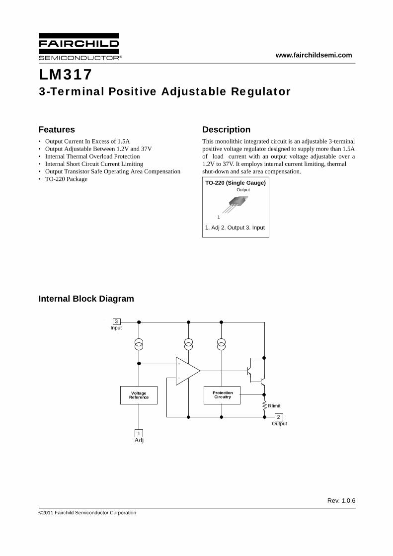
©2011 Fairchild Semiconductor Corporation www.fairchildsemi.com Rev. 1.0.6 Features • Output Current In Excess of 1.5A • Output Adjustable Between 1.2V and 37V • Internal Thermal Overload Protection • Internal Short Circuit Current Limiting • Output Transistor Safe Operating Area Compensation • TO-220 Package Description This monolithic integrated circuit is an adjustable 3-terminal positive voltage regulator designed to supply more than 1.5A of load current with an output voltage adjustable over a 1.2V to 37V. It employs internal current limiting, thermal shut-down and safe area compensation. TO-220 (Single Gauge) 1. Adj 2. Output 3. Input 1 Output Internal Block Diagram Rlimit 3 1 Voltage Reference Vadj 2 Protection Circuitry + - Input Output Adj LM317 3-Terminal Positive Adjustable Regulator
-
Upload
gerson-villa-gonzalez -
Category
Documents
-
view
216 -
download
3
description
Hoja de Especificaciones LM317
Transcript of LM317
©2011 Fairchild Semiconductor Corporation
www.fairchildsemi.com
Rev. 1.0.6
Features• Output Current In Excess of 1.5A• Output Adjustable Between 1.2V and 37V• Internal Thermal Overload Protection• Internal Short Circuit Current Limiting• Output Transistor Safe Operating Area Compensation• TO-220 Package
DescriptionThis monolithic integrated circuit is an adjustable 3-terminalpositive voltage regulator designed to supply more than 1.5Aof load current with an output voltage adjustable over a1.2V to 37V. It employs internal current limiting, thermal shut-down and safe area compensation.
TO-220 (Single Gauge)
1. Adj 2. Output 3. Input
1
Output
Internal Block Diagram
Rlimit
3Vin
Vo
1
VoltageReference
Vadj
2
ProtectionCircuitry
+
-
Input
Output
Adj
LM3173-Terminal Positive Adjustable Regulator
LM317
2
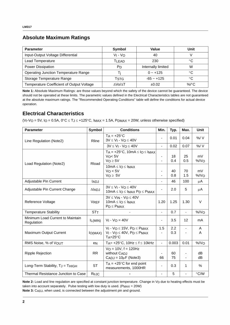
Absolute Maximum Ratings
Note 1: Absolute Maximum Ratings: are those values beyond which the safety of the device cannot be guaranteed. The deviceshould not be operated at these limits. The parametric values defined in the Electrical Characteristics tables are not guaranteedat the absolute maximum ratings. The "Recommended Operating Conditions" table will define the conditions for actual deviceoperation.
Electrical Characteristics(VI-VO = 5V, IO = 0.5A, 0°C ≤ TJ ≤ +125°C, IMAX = 1.5A, PDMAX = 20W, unless otherwise specified)
Note 2: Load and line regulation are specified at constant junction temperature. Change in VD due to heating effects must betaken into account separately. Pulse testing with low duty is used. (PMAX = 20W)Note 3: CADJ, when used, is connected between the adjustment pin and ground.
Parameter Symbol Value UnitInput-Output Voltage Differential VI - VO 40 VLead Temperature TLEAD 230 °CPower Dissipation PD Internally limited WOperating Junction Temperature Range Tj 0 ~ +125 °CStorage Temperature Range TSTG -65 ~ +125 °CTemperature Coefficient of Output Voltage ΔVo/ΔT ±0.02 %/°C
Parameter Symbol Conditions Min. Typ. Max. Unit
Line Regulation (Note2) RlineTA = +25°C3V ≤ VI - VO ≤ 40V - 0.01 0.04 %/ V
3V ≤ VI - VO ≤ 40V - 0.02 0.07 %/ V
Load Regulation (Note2) Rload
TA = +25°C, 10mA ≤ IO ≤ IMAXVO< 5VVO ≥ 5V
--
180.4
250.5
mV%/VO
10mA ≤ IO ≤ IMAXVO < 5VVO ≥ 5V
--
400.8
701.5
mV%/VO
Adjustable Pin Current IADJ - - 46 100 μA
Adjustable Pin Current Change ΔIADJ3V ≤ VI - VO ≤ 40V10mA ≤ IO ≤ IMAX PD ≤ PMAX
- 2.0 5 μA
Reference Voltage VREF3V ≤ VIN - VO ≤ 40V10mA ≤ IO ≤ IMAXPD ≤ PMAX
1.20 1.25 1.30 V
Temperature Stability STT - - 0.7 - %/VO
Minimum Load Current to Maintain Regulation IL(MIN) VI - VO = 40V - 3.5 12 mA
Maximum Output Current IO(MAX)VI - VO ≤ 15V, PD ≤ PMAXVI - VO ≤ 40V, PD ≤ PMAX TA=25°C
1.5-
2.20.3
--
AA
RMS Noise, % of VOUT eN TA= +25°C, 10Hz ≤ f ≤ 10kHz - 0.003 0.01 %/VO
Ripple Rejection RRVO = 10V, f = 120Hzwithout CADJCADJ = 10μF (Note3)
-66
6075
--
dBdB
Long-Term Stability, TJ = THIGH ST TA = +25°C for end pointmeasurements, 1000HR - 0.3 1 %
Thermal Resistance Junction to Case RθJC - - 5 - °C/W
LM317
3
Typical Performance Characteristics
Figure 1. Load Regulation
Figure 3. Dropout Voltage
Figure 2. Adjustment Current
Figure 4. Reference Voltage
TEMPERATURE (°C)
OU
TPU
T V
OLT
AG
E D
EV
IATI
ON
(%)
TEMPERATURE (°C)
INP
UT-
OU
TPU
T D
IFFE
RE
NTI
AL(V
)
TEMPERATURE (°C)
AD
JUS
TME
NT
CU
RR
EN
T(uA
)
TEMPERATURE (°C)
RE
FER
EN
CE
VO
LTA
GE(
V)
LM317
4
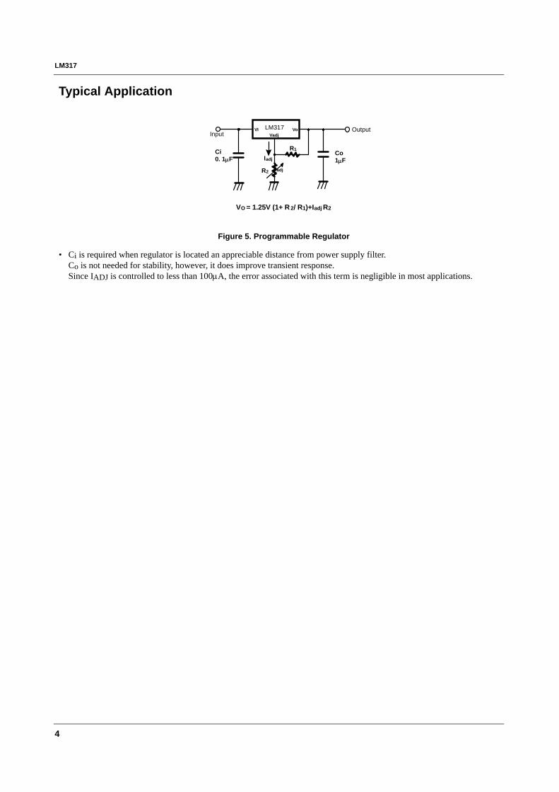
Typical Application
Figure 5. Programmable Regulator
• Ci is required when regulator is located an appreciable distance from power supply filter. Co is not needed for stability, however, it does improve transient response. Since IADJ is controlled to less than 100μA, the error associated with this term is negligible in most applications.
VI KA317
Ci0. 1μF
VI VoVadj
R2
Iadj
VO = 1.25V (1+ R 2/ R1)+Iadj R2
R1
Iadj
Co1μF
InputOutputLM317
LM317
5
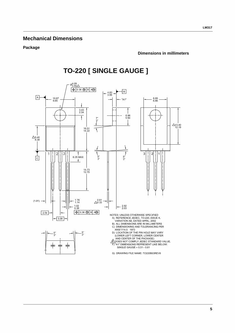
Mechanical DimensionsPackage
Dimensions in millimeters
TO-220 [ SINGLE GAUGE ]
LM317
10/17/11 0.0m 001Stock#DS400281
© 2011 Fairchild Semiconductor Corporation
LIFE SUPPORT POLICY FAIRCHILD’S PRODUCTS ARE NOT AUTHORIZED FOR USE AS CRITICAL COMPONENTS IN LIFE SUPPORT DEVICES OR SYSTEMS WITHOUT THE EXPRESS WRITTEN APPROVAL OF THE PRESIDENT OF FAIRCHILD SEMICONDUCTOR CORPORATION. As used herein:
1. Life support devices or systems are devices or systems which, (a) are intended for surgical implant into the body, or (b) support or sustain life, and (c) whose failure to perform when properly used in accordance with instructions for use provided in the labeling, can be reasonably expected to result in a significant injury of the user.
2. A critical component in any component of a life support device or system whose failure to perform can be reasonably expected to cause the failure of the life support device or system, or to affect its safety or effectiveness.
www.fairchildsemi.com
DISCLAIMER FAIRCHILD SEMICONDUCTOR RESERVES THE RIGHT TO MAKE CHANGES WITHOUT FURTHER NOTICE TO ANY PRODUCTS HEREIN TO IMPROVE RELIABILITY, FUNCTION OR DESIGN. FAIRCHILD DOES NOT ASSUME ANY LIABILITY ARISING OUT OF THE APPLICATION OR USE OF ANY PRODUCT OR CIRCUIT DESCRIBED HEREIN; NEITHER DOES IT CONVEY ANY LICENSE UNDER ITS PATENT RIGHTS, NOR THE RIGHTS OF OTHERS.
Ordering InformationProduct Number Package Operating Temperature
LM317T TO-220 (Single Gauge) 0°C to +125°C


