LM2731 0.6/1.6-MHz Boost Converters With 22-V Internal … · Product Folder Sample & Buy Technical...
31
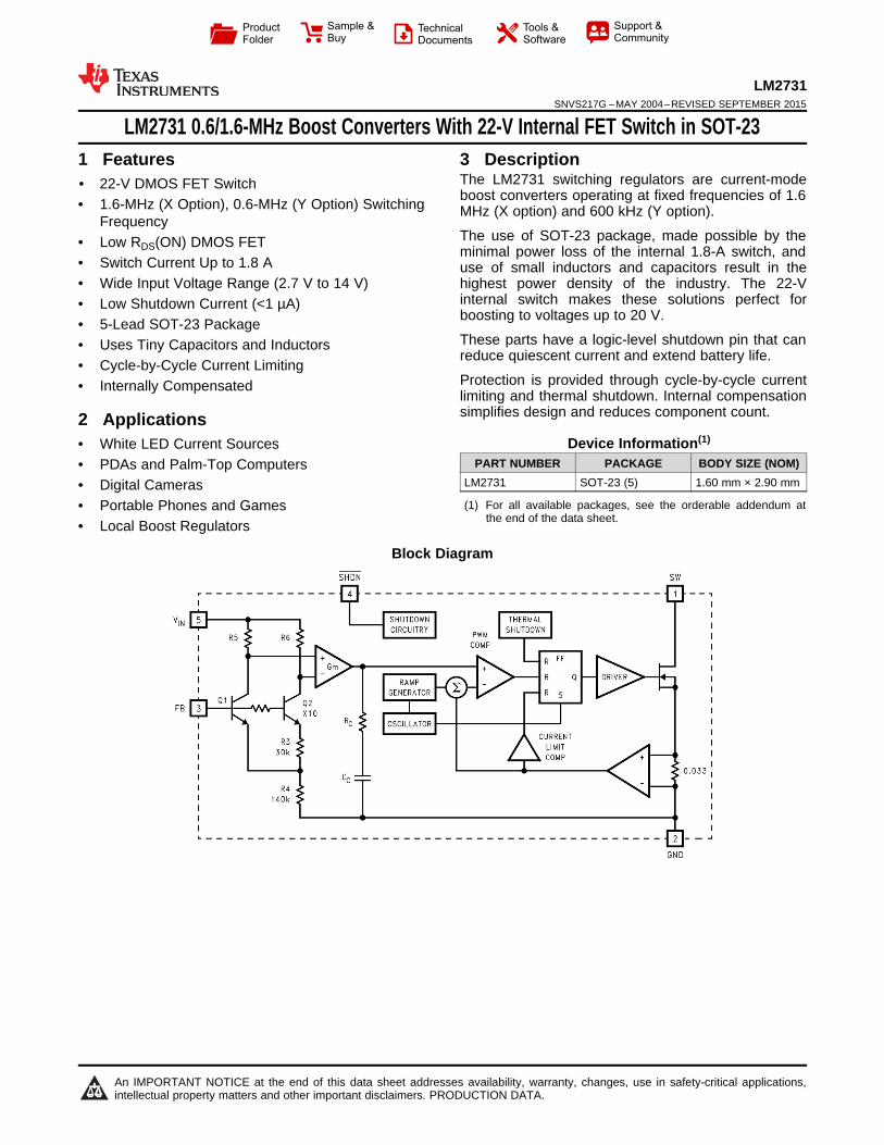
Product Folder Sample & Buy Technical Documents Tools & Software Support & Community LM2731 SNVS217G – MAY 2004 – REVISED SEPTEMBER 2015 LM2731 0.6/1.6-MHz Boost Converters With 22-V Internal FET Switch in SOT-23 1 Features 3 Description The LM2731 switching regulators are current-mode 1• 22-V DMOS FET Switch boost converters operating at fixed frequencies of 1.6 • 1.6-MHz (X Option), 0.6-MHz (Y Option) Switching MHz (X option) and 600 kHz (Y option). Frequency The use of SOT-23 package, made possible by the • Low R DS (ON) DMOS FET minimal power loss of the internal 1.8-A switch, and • Switch Current Up to 1.8 A use of small inductors and capacitors result in the • Wide Input Voltage Range (2.7 V to 14 V) highest power density of the industry. The 22-V internal switch makes these solutions perfect for • Low Shutdown Current (<1 μA) boosting to voltages up to 20 V. • 5-Lead SOT-23 Package These parts have a logic-level shutdown pin that can • Uses Tiny Capacitors and Inductors reduce quiescent current and extend battery life. • Cycle-by-Cycle Current Limiting Protection is provided through cycle-by-cycle current • Internally Compensated limiting and thermal shutdown. Internal compensation simplifies design and reduces component count. 2 Applications Device Information (1) • White LED Current Sources PART NUMBER PACKAGE BODY SIZE (NOM) • PDAs and Palm-Top Computers LM2731 SOT-23 (5) 1.60 mm × 2.90 mm • Digital Cameras (1) For all available packages, see the orderable addendum at • Portable Phones and Games the end of the data sheet. • Local Boost Regulators Block Diagram 1 An IMPORTANT NOTICE at the end of this data sheet addresses availability, warranty, changes, use in safety-critical applications, intellectual property matters and other important disclaimers. PRODUCTION DATA.
Transcript of LM2731 0.6/1.6-MHz Boost Converters With 22-V Internal … · Product Folder Sample & Buy Technical...
Product
Folder
Sample &Buy
Technical
Documents
Tools &
Software
Support &Community
LM2731SNVS217G –MAY 2004–REVISED SEPTEMBER 2015
LM2731 0.6/1.6-MHz Boost Converters With 22-V Internal FET Switch in SOT-231 Features 3 Description
The LM2731 switching regulators are current-mode1• 22-V DMOS FET Switch
boost converters operating at fixed frequencies of 1.6• 1.6-MHz (X Option), 0.6-MHz (Y Option) Switching MHz (X option) and 600 kHz (Y option).Frequency
The use of SOT-23 package, made possible by the• Low RDS(ON) DMOS FET minimal power loss of the internal 1.8-A switch, and• Switch Current Up to 1.8 A use of small inductors and capacitors result in the• Wide Input Voltage Range (2.7 V to 14 V) highest power density of the industry. The 22-V
internal switch makes these solutions perfect for• Low Shutdown Current (<1 µA)boosting to voltages up to 20 V.• 5-Lead SOT-23 PackageThese parts have a logic-level shutdown pin that can• Uses Tiny Capacitors and Inductorsreduce quiescent current and extend battery life.
• Cycle-by-Cycle Current LimitingProtection is provided through cycle-by-cycle current• Internally Compensatedlimiting and thermal shutdown. Internal compensationsimplifies design and reduces component count.2 Applications
Device Information(1)• White LED Current SourcesPART NUMBER PACKAGE BODY SIZE (NOM)• PDAs and Palm-Top Computers
LM2731 SOT-23 (5) 1.60 mm × 2.90 mm• Digital Cameras(1) For all available packages, see the orderable addendum at• Portable Phones and Games
the end of the data sheet.• Local Boost Regulators
Block Diagram
1
An IMPORTANT NOTICE at the end of this data sheet addresses availability, warranty, changes, use in safety-critical applications,intellectual property matters and other important disclaimers. PRODUCTION DATA.

LM2731SNVS217G –MAY 2004–REVISED SEPTEMBER 2015 www.ti.com
Table of Contents1 Features .................................................................. 1 8 Application and Implementation ........................ 13
8.1 Application Information............................................ 132 Applications ........................................................... 18.2 Typical Application .................................................. 133 Description ............................................................. 18.3 System Examples ................................................... 184 Revision History..................................................... 2
9 Power Supply Recommendations ...................... 205 Pin Configuration and Functions ......................... 310 Layout................................................................... 206 Specifications......................................................... 3
10.1 Layout Guidelines ................................................. 206.1 Absolute Maximum Ratings ...................................... 310.2 Layout Example .................................................... 206.2 ESD Ratings.............................................................. 310.3 Thermal Considerations ........................................ 216.3 Recommended Operating Conditions....................... 4
11 Device and Documentation Support ................. 226.4 Thermal Information .................................................. 411.1 Device Support...................................................... 226.5 Electrical Characteristics........................................... 511.2 Community Resources.......................................... 226.6 Typical Characteristics .............................................. 711.3 Trademarks ........................................................... 227 Detailed Description ............................................ 1111.4 Electrostatic Discharge Caution............................ 227.1 Overview ................................................................. 1111.5 Glossary ................................................................ 227.2 Functional Block Diagram ....................................... 11
12 Mechanical, Packaging, and Orderable7.3 Feature Description................................................. 11Information ........................................................... 227.4 Device Functional Modes........................................ 12
4 Revision HistoryNOTE: Page numbers for previous revisions may differ from page numbers in the current version.
Changes from Revision F (November 2012) to Revision G Page
• Added ESD Ratings table, Feature Description section, Device Functional Modes, Application and Implementationsection, Power Supply Recommendations section, Layout section, Device and Documentation Support section, andMechanical, Packaging, and Orderable Information section. ................................................................................................ 1
2 Submit Documentation Feedback Copyright © 2004–2015, Texas Instruments Incorporated
Product Folder Links: LM2731

J A A
J A
T (MAX) T 125 TP (MAX)
265-
- -= =
q
3
FB
2
GND
1
SW
4 5
SHDN VIN
formula: . If power dissipation exceeds the maximum specified above, the internal thermal
LM2731www.ti.com SNVS217G –MAY 2004–REVISED SEPTEMBER 2015
5 Pin Configuration and Functions
DBV Package5-Pin SOT-23
Top View
Pin FunctionsPIN
I/O DESCRIPTIONNAME NO.FB 3 I Feedback point that connects to external resistive divider.GND 2 PWR Analog and power groundSHDN 4 I Shutdown control input. Connect to VIN if the feature is not used.SW 1 O Drain of the internal FET switchVIN 5 PWR Analog and power input
6 Specifications
6.1 Absolute Maximum Ratings (1)
MIN MAX UNITOperating Junction Temperature –40 125 °CLead Temperature (Soldering, 5 sec.) 300 °CPower Dissipation (2) Internally LimitedFB Pin Voltage –0.4 6 VSW Pin Voltage –0.4 22 VInput Supply Voltage –0.4 14.5 VSHDN Pin Voltage –0.4 VIN + 0.3 VStorage Temperature, Tstg –65 150 °C
(1) Stresses beyond those listed under Absolute Maximum Ratings may cause permanent damage to the device. These are stress ratingsonly, which do not imply functional operation of the device at these or any other conditions beyond those indicated under RecommendedOperating Conditions. Exposure to absolute-maximum-rated conditions for extended periods may affect device reliability.
(2) The maximum power dissipation which can be safely dissipated for any application is a function of the maximum junction temperature,TJ(MAX) = 125°C, the junction-to-ambient thermal resistance for the SOT-23 package, RθJA = 265°C/W, and the ambient temperature,TA. The maximum allowable power dissipation at any ambient temperature for designs using this device can be calculated using the
protection circuitry will protect the device by reducing the output voltage as required to maintain a safe junction temperature.
6.2 ESD RatingsVALUE UNIT
V(ESD) Electrostatic discharge Human body model (HBM), per ANSI/ESDA/JEDEC JS-001 (1) (2) ±2000 V
(1) JEDEC document JEP155 states that 500-V HBM allows safe manufacturing with a standard ESD control process.(2) The human body model is a 100-pF capacitor discharged through a 1.5-kΩ resistor into each pin.
Copyright © 2004–2015, Texas Instruments Incorporated Submit Documentation Feedback 3
Product Folder Links: LM2731

LM2731SNVS217G –MAY 2004–REVISED SEPTEMBER 2015 www.ti.com
6.3 Recommended Operating Conditionsover operating free-air temperature range (unless otherwise noted)
MIN NOM MAX UNITVIN Input Supply Voltage 2.7 14 VVsw SW Pin Voltage 3 20 VVshdn Shutdown Supply Voltage (1) 0 VIN VTJ Junction Temperature Range –40 125 ºC
(1) This pin should not be allowed to float or be greater than VIN + 0.3 V.
6.4 Thermal InformationLM2731
THERMAL METRIC (1) DBV (SOT-23) UNIT5 PINS
RθJA Junction-to-ambient thermal resistance 209.9 °C/WRθJC(top) Junction-to-case (top) thermal resistance 122 °C/WRθJB Junction-to-board thermal resistance 38.4 °C/WψJT Junction-to-top characterization parameter 12.8 °C/WψJB Junction-to-board characterization parameter 37.5 °C/WRθJC(bot) Junction-to-case (bottom) thermal resistance N/A °C/W
(1) For more information about traditional and new thermal metrics, see the Semiconductor and IC Package Thermal Metrics applicationreport, SPRA953.
4 Submit Documentation Feedback Copyright © 2004–2015, Texas Instruments Incorporated
Product Folder Links: LM2731

LM2731www.ti.com SNVS217G –MAY 2004–REVISED SEPTEMBER 2015
6.5 Electrical CharacteristicsLimits are for TJ = 25°C. Unless otherwise specified: VIN = 5 V, VSHDN = 5 V, IL = 0 A.
PARAMETER TEST CONDITIONS MIN (1) TYP (2) MAX (1) UNIT
VIN Input Voltage −40°C ≤ TJ ≤ 125°C 2.7 14 V
VIN = 2.7 V 7
−40°C ≤ TJ ≤ 5.4125°CRL = 43 Ω VIN = 3.3 V 10X Option (3)
−40°C ≤ TJ ≤ 8125°C
VIN = 5 V 16
VIN = 2.7 V 7.5
−40°C ≤ TJ ≤ 6125°CRL = 43 Ω VIN = 3.3 V 11Y Option (3)
−40°C ≤ TJ ≤ 8.75125°C
VIN = 5 V 15VOUT (MIN) Minimum Output Voltage Under Load V
VIN = 2.7 V 5
−40°C ≤ TJ ≤ 3.75125°CRL = 15 Ω VIN = 3.3 V 6.5X Option (3)
−40°C ≤ TJ ≤ 5125°C
VIN = 5 V 10
VIN = 2.7 V 5
−40°C ≤ TJ ≤ 4125°CRL = 15 Ω VIN = 3.3 V 7Y Option (3)
−40°C ≤ TJ ≤ 5.5125°C
VIN = 5 V 10
TJ = 25°C 1.8 2ISW Switch Current Limit See (4) A−40°C ≤ TJ ≤ 1.4125°C
TJ = 25°C 260 400ISW = 100 mA
−40°C ≤ TJ ≤Vin = 5 V 500125°CRDS(ON) Switch ON-Resistance mΩ
TJ = 25°C 300 450ISW = 100 mA
−40°C ≤ TJ ≤Vin = 3.3 V 550125°C
−40°C ≤ TJ ≤Device ON 1.5125°CSHDNTH Shutdown Threshold V
−40°C ≤ TJ ≤Device OFF 0.5125°C
VSHDN = 0 0
TJ = 25°C 0ISHDN Shutdown Pin Bias Current µAVSHDN = 5 V −40°C ≤ TJ ≤ 2125°C
TJ = 25°C 1.230VFB Feedback Pin Reference Voltage VIN = 3 V V−40°C ≤ TJ ≤ 1.205 1.255125°C
TJ = 25°C 60IFB Feedback Pin Bias Current VFB = 1.23 V nA−40°C ≤ TJ ≤ 500125°C
(1) Limits are ensured by testing, statistical correlation, or design.(2) Typical values are derived from the mean value of a large quantity of samples tested during characterization and represent the most
likely expected value of the parameter at room temperature.(3) L = 10 µH, COUT = 4.7 µF, duty cycle = maximum(4) Switch current limit is dependent on duty cycle (see Typical Characteristics).
Copyright © 2004–2015, Texas Instruments Incorporated Submit Documentation Feedback 5
Product Folder Links: LM2731

LM2731SNVS217G –MAY 2004–REVISED SEPTEMBER 2015 www.ti.com
Electrical Characteristics (continued)Limits are for TJ = 25°C. Unless otherwise specified: VIN = 5 V, VSHDN = 5 V, IL = 0 A.
PARAMETER TEST CONDITIONS MIN (1) TYP (2) MAX (1) UNIT
TJ = 25°C 2VSHDN = 5 V, Switching
−40°C ≤ TJ ≤"X" 3125°CmA
TJ = 25°C 1VSHDN = 5 V, Switching
−40°C ≤ TJ ≤"Y"IQ Quiescent Current 2125°C
TJ = 25°C 400VSHDN = 5 V, Not
−40°C ≤ TJ ≤Switching 500 µA125°C
VSHDN = 0 0.024 1
ΔVFB/ΔVIN FB Voltage Line Regulation 2.7 V ≤ VIN ≤ 14 V 0.02 %/V
TJ = 25°C 1.6“X” Option −40°C ≤ TJ ≤ 1 1.85125°C
FSW Switching Frequency (5) MHzTJ = 25°C 0.6
“Y” Option −40°C ≤ TJ ≤ 0.4 0.8125°C
TJ = 25°C 86%“X” Option −40°C ≤ TJ ≤ 78%125°C
DMAX Maximum Duty Cycle (5)
TJ = 25°C 93%“Y” Option −40°C ≤ TJ ≤ 88%125°C
IL Switch Leakage Not Switching VSW = 5 V 1 µA
(5) Specified limits are the same for Vin = 3.3 V input.
6 Submit Documentation Feedback Copyright © 2004–2015, Texas Instruments Incorporated
Product Folder Links: LM2731
TEMPERATURE (oC)
OS
CIL
LAT
OR
FR
EQ
UE
NC
Y (
MH
z)
0.48
0.5
0.52
0.54
0.56
0.58
0.6
VIN = 5V
VIN = 3.3V
-50 -25 0 25 50 75 100 125 15095.9
96
96.1
96.2
96.3
96.4
96.5
96.6
96.7
96.8
MA
X D
UT
Y C
YC
LE (
%)
TEMPERATURE (oC)
VIN = 5V
VIN = 3.3V
-50 -25 0 25 50 75 100 125 150
OS
CIL
LAT
OR
FR
EQ
UE
NC
Y (
MH
z)
1.4
1.42
1.44
1.46
1.48
1.5
1.52
1.54
1.56
1.58
TEMPERATURE (oC)
VIN = 5V
VIN = 3.3V
-50 -25 0 25 50 75 100 125 150
TEMPERATURE (oC)
OS
CIL
LAT
OR
FR
EQ
UE
NC
Y (
MH
z)
0.48
0.5
0.52
0.54
0.56
0.58
0.6
VIN = 5V
VIN = 3.3V
-50 -25 0 25 50 75 100 125 150
-50 -25 0 25 50 75 100 125 150
TEMPERATURE (oC)
1.8
1.85
1.9
1.95
2
2.05
2.1
2.15
2.2
I Q V
IN A
CT
IVE
(m
A)
0.9
0.95
1
1.05
1.1
1.15
1.2
1.25
TEMPERATURE (oC)
I Q V
IN A
CT
IVE
(m
A)
-50 -25 0 25 50 75 100 125 150
LM2731www.ti.com SNVS217G –MAY 2004–REVISED SEPTEMBER 2015
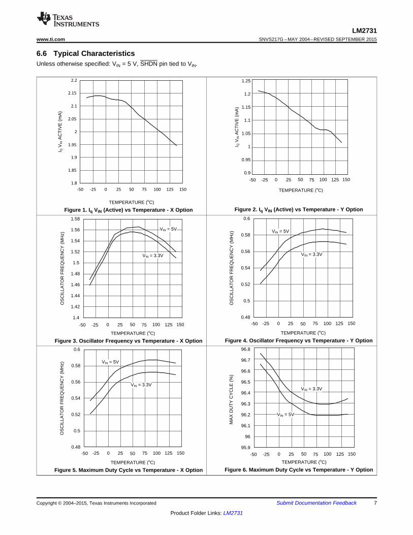
6.6 Typical CharacteristicsUnless otherwise specified: VIN = 5 V, SHDN pin tied to VIN.
Figure 2. Iq VIN (Active) vs Temperature - Y OptionFigure 1. Iq VIN (Active) vs Temperature - X Option
Figure 4. Oscillator Frequency vs Temperature - Y OptionFigure 3. Oscillator Frequency vs Temperature - X Option
Figure 6. Maximum Duty Cycle vs Temperature - Y OptionFigure 5. Maximum Duty Cycle vs Temperature - X Option
Copyright © 2004–2015, Texas Instruments Incorporated Submit Documentation Feedback 7
Product Folder Links: LM2731

2.5 3.5 4.5 5.5 6.5 7.5 8.5 9.5
VIN (V)
0
50
100
150
200
250
300
350
RD
S_O
N (
m:
)
CU
RR
EN
T L
IMIT
(A
)
2
2.1
2.2
2.3
2.4
2.5
2.6
-40 -25 0 25 50 75 100 125
TEMPERATURE (oC)
FE
ED
BA
CK
VO
LTA
GE
(V
)
1.222
1.223
1.224
1.225
1.226
1.227
1.228
1.229
1.23
1.231
-40 -25 0 25 50 75 100 125
TEMPERATURE (oC)
RD
S(O
N) (:
)
-40 -25 0 25 50 75 100 125
TEMPERATURE (oC)
0
0.05
0.1
0.15
0.2
0.25
0.3
0.35
0.4
0.45
0.5
Vin = 5V
Vin = 3.3V
I Q V
IN (
IDLE
) (P
A)
TEMPERATURE (oC)
340
345
350
355
360
365
370
375
380
-50 -25 0 25 50 75 100 125 150
TEMPERATURE (oC)
FE
ED
BA
CK
BIA
S C
UR
RE
NT
(P
A)
0
0.01
0.02
0.03
0.04
0.05
0.06
0.07
0.08
0.09
-50 -25 0 25 50 75 100 125 150
LM2731SNVS217G –MAY 2004–REVISED SEPTEMBER 2015 www.ti.com
Typical Characteristics (continued)Unless otherwise specified: VIN = 5 V, SHDN pin tied to VIN.
Figure 8. Feedback Bias Current vs TemperatureFigure 7. Iq VIN (Idle) vs Temperature
Figure 9. Feedback Voltage vs Temperature Figure 10. RDS(ON) vs Temperature
Figure 11. Current Limit vs Temperature Figure 12. RDS(ON) vs VIN
8 Submit Documentation Feedback Copyright © 2004–2015, Texas Instruments Incorporated
Product Folder Links: LM2731
3500 50 100 150 200 250 300
LOAD (mA)
EF
FIC
IEN
CY
(%
)
0
10
20
30
40
50
60
70
80
90
100
EF
FIC
IEN
CY
(%
)
0
10
20
30
40
50
60
70
80
90
100
3500 50 100 150 200 250 300
LOAD (mA)
400
6000 100 200 300 400 500
LOAD (mA)
EF
FIC
IEN
CY
(%
)
0
10
20
30
40
50
60
70
80
90
100
0 10 20 30 40 50
0
10
20
30
40
50
60
70
80
EF
FIC
IEN
CY
(%
)
LOAD (mA)
14000 200 400 600 800 1000 1200
LOAD (mA)
EF
FIC
IEN
CY
(%
)
0
10
20
30
40
50
60
70
80
90
100
0 50 100 150 200 250 300
LOAD (mA)
EF
FIC
IEN
CY
(%
)
0
10
20
30
40
50
60
70
80
90
100
LM2731www.ti.com SNVS217G –MAY 2004–REVISED SEPTEMBER 2015
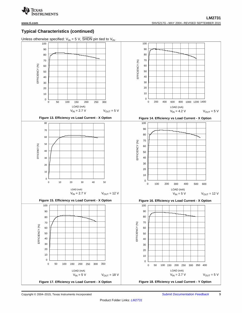
Typical Characteristics (continued)Unless otherwise specified: VIN = 5 V, SHDN pin tied to VIN.
VIN = 2.7 V VOUT = 5 V VIN = 4.2 V VOUT = 5 V
Figure 13. Efficiency vs Load Current - X Option Figure 14. Efficiency vs Load Current - X Option
VIN = 2.7 V VOUT = 12 V VIN = 5 V VOUT = 12 V
Figure 15. Efficiency vs Load Current - X Option Figure 16. Efficiency vs Load Current - X Option
VIN = 2.7 V VOUT = 5 VVIN = 5 V VOUT = 18 V
Figure 18. Efficiency vs Load Current - Y OptionFigure 17. Efficiency vs Load Current - X Option
Copyright © 2004–2015, Texas Instruments Incorporated Submit Documentation Feedback 9
Product Folder Links: LM2731

0 100 200 300 400 500 600
LOAD (mA)
EF
FIC
IEN
CY
(%
)
0
10
20
30
40
50
60
70
80
90
100
EF
FIC
IEN
CY
(%
)
0 50 100 150 200 250
LOAD (mA)
0
10
20
30
40
50
60
70
80
90
100
0 20 40 60 80
LOAD (mA)
EF
FIC
IEN
CY
(%
)
0
10
20
30
40
50
60
70
80
90
100
14000 200 400 600 800 1000 1200
LOAD (mA)
EF
FIC
IEN
CY
(%
)
0
10
20
30
40
50
60
70
80
90
100
14000 200 400 600 800 1000 1200
LOAD (mA)
EF
FIC
IEN
CY
(%
)
0
10
20
30
40
50
60
70
80
90
100
LM2731SNVS217G –MAY 2004–REVISED SEPTEMBER 2015 www.ti.com
Typical Characteristics (continued)Unless otherwise specified: VIN = 5 V, SHDN pin tied to VIN.
VIN = 4.2 V VOUT = 5 VVIN = 3.3 V VOUT = 5 V
Figure 19. Efficiency vs Load Current - Y Option Figure 20. Efficiency vs Load Current - Y Option
VIN = 2.7 V VOUT = 12 V VIN = 3.3 V VOUT = 12 V
Figure 21. Efficiency vs Load Current - Y Option Figure 22. Efficiency vs Load Current - Y Option
VIN = 5 V VOUT = 12 V
Figure 23. Efficiency vs Load Current - Y Option
10 Submit Documentation Feedback Copyright © 2004–2015, Texas Instruments Incorporated
Product Folder Links: LM2731

LM2731www.ti.com SNVS217G –MAY 2004–REVISED SEPTEMBER 2015
7 Detailed Description
7.1 OverviewThe LM2731 device is a switching converter IC that operates at a fixed frequency (0.6 or 1.6 MHz) for fasttransient response over a wide input voltage range and incorporates pulse-by-pulse current limiting protection.Because this is current mode control, a 33-mΩ sense resistor in series with the switch FET is used to provide avoltage (which is proportional to the FET current) to both the input of the pulse width modulation (PWM)comparator and the current limit amplifier.
7.1.1 Theory of OperationAt the beginning of each cycle, the S-R latch turns on the FET. As the current through the FET increases, avoltage (proportional to this current) is summed with the ramp coming from the ramp generator and then fed intothe input of the PWM comparator. When this voltage exceeds the voltage on the other input (coming from theGm amplifier), the latch resets and turns the FET off. Because the signal coming from the Gm amplifier is derivedfrom the feedback (which samples the voltage at the output), the action of the PWM comparator constantly setsthe correct peak current through the FET to keep the output voltage in regulation.
Q1 and Q2 along with R3 - R6 form a bandgap voltage reference used by the IC to hold the output in regulation.The currents flowing through Q1 and Q2 will be equal, and the feedback loop will adjust the regulated output tomaintain this. Because of this, the regulated output is always maintained at a voltage level equal to the voltage atthe FB node "multiplied up" by the ratio of the output resistive-divider.
The current limit comparator feeds directly into the flip-flop that drives the switch FET. If the FET current reachesthe limit threshold, the FET is turned off and the cycle terminated until the next clock pulse. The current limitinput terminates the pulse regardless of the status of the output of the PWM comparator.
7.2 Functional Block Diagram
7.3 Feature DescriptionThe LM2731 is a fixed-frequency boost regulator IC that delivers a minimum 1.8-A peak switch current.
The device provides cycle-by-cycle current limit protection as well as thermal shutdown protection. The devicecan also be controlled through the shutdown pin.
Copyright © 2004–2015, Texas Instruments Incorporated Submit Documentation Feedback 11
Product Folder Links: LM2731

LM2731SNVS217G –MAY 2004–REVISED SEPTEMBER 2015 www.ti.com
7.4 Device Functional Modes
7.4.1 Shutdown Pin OperationThe device is turned off by pulling the shutdown pin low. If this function is not going to be used, the pin should betied directly to VIN. If the SHDN function will be needed, a pullup resistor must be used to VIN (approximately 50kΩ to 100 kΩ recommended). The SHDN pin must not be left unterminated.
7.4.2 Thermal ShutdownThermal shutdown limits total power dissipation by turning off the output switch when the IC junction temperatureexceeds 160°C. After thermal shutdown occurs, the output switch doesn’t turn on until the junction temperaturedrops to approximately 150°C.
7.4.3 Current LimitThe LM2731 uses cycle-by-cycle current limiting to protect the internal NMOS switch. It is important to note thatthis current limit will not protect the output from excessive current during an output short-circuit. The input supplyis connected to the output by the series connection of an inductor and a diode. If a short circuit is placed on theoutput, excessive current can damage both the inductor and diode.
12 Submit Documentation Feedback Copyright © 2004–2015, Texas Instruments Incorporated
Product Folder Links: LM2731

EF
FIC
IEN
CY
(%
)
LOAD CURRENT (mA)
0 100 200 300 400
70
80
90
100
500
5 - 12V Boost
^y_s]v
LM2731 ³;´
SW
FB
GND
VIN
SHDN
U1
R3
51KSHDN
GND
5 VIN
C12.2PF R2
13.3K
CF220pF
D1
MBR0520
R1/117K
L1/10PH
C24.7PF
12V
OUT
500mA
(TYP)
LM2731www.ti.com SNVS217G –MAY 2004–REVISED SEPTEMBER 2015
8 Application and Implementation
NOTEInformation in the following applications sections is not part of the TI componentspecification, and TI does not warrant its accuracy or completeness. TI’s customers areresponsible for determining suitability of components for their purposes. Customers shouldvalidate and test their design implementation to confirm system functionality.
8.1 Application InformationThe device will operate with input voltage range from 2.7 V to 14 V and provide a regulated output voltage. Thisdevice is optimized for high-efficiency operation with minimum number of external components. For componentselection, see Detailed Design Procedure.
8.2 Typical Application
Figure 24. Application Schematic Figure 25. Efficiency vs Load Current
8.2.1 Design RequirementsThe device must be able to operate at any voltage within the recommended operating range. The load currentmust be defined in order to properly size the inductor, input, and output capacitors. The inductor must be able tohandle full expected load current as well as the peak current generated during load transients and start-up.Inrush current at start-up will depend on the output capacitor selection. More details are provided in DetailedDesign Procedure.
The device has a shutdown pin which is used to disable the device. This pin is active-LOW and care must betaken that the voltage on this pin does not exceed VIN + 0.3 V. This pin must also not be left floating.
8.2.2 Detailed Design Procedure
8.2.2.1 Selecting the External CapacitorsThe best capacitors for use with the LM2731 are multi-layer ceramic capacitors. These capacitors have thelowest ESR (equivalent series resistance) and highest resonance frequency which makes them optimum for usewith high-frequency switching converters.
When selecting a ceramic capacitor, only X5R and X7R dielectric types should be used. Other types such asZ5U and Y5F have such severe loss of capacitance due to effects of temperature variation and applied voltage,they may provide as little as 20% of rated capacitance in many typical applications. Always consult capacitormanufacturer’s data curves before selecting a capacitor. High-quality ceramic capacitors can be obtained fromTaiyo-Yuden, AVX, and Murata.
Copyright © 2004–2015, Texas Instruments Incorporated Submit Documentation Feedback 13
Product Folder Links: LM2731
LM2731SNVS217G –MAY 2004–REVISED SEPTEMBER 2015 www.ti.com
8.2.2.2 Selecting the Output CapacitorA single ceramic capacitor of value 4.7 µF to 10 µF will provide sufficient output capacitance for mostapplications. If larger amounts of capacitance are desired for improved line support and transient response,tantalum capacitors can be used. Aluminum electrolytics with ultra low ESR such as Sanyo Oscon can be used,but are usually prohibitively expensive. Typical AI electrolytic capacitors are not suitable for switching frequenciesabove 500 kHz due to significant ringing and temperature rise due to self-heating from ripple current. An outputcapacitor with excessive ESR can also reduce phase margin and cause instability.
In general, if electrolytics are used, TI recommends that they be paralleled with ceramic capacitors to reduceringing, switching losses, and output voltage ripple.
8.2.2.3 Selecting the Input CapacitorAn input capacitor is required to serve as an energy reservoir for the current which must flow into the coil eachtime the switch turns ON. This capacitor must have extremely low ESR, so ceramic is the best choice. TIrecommends a nominal value of 2.2 µF, but larger values can be used. Since this capacitor reduces the amountof voltage ripple seen at the input pin, it also reduces the amount of EMI passed back along that line to othercircuitry.
8.2.2.4 Feedforward CompensationAlthough internally compensated, the feedforward capacitor Cf is required for stability (see Figure 26). Addingthis capacitor puts a zero in the loop response of the converter. The recommended frequency for the zero fzshould be approximately 6 kHz. Cf can be calculated using the formula:
Cf = 1 / (2 × π X R1 × fz) (1)
8.2.2.5 Selecting DiodesThe external diode used in the typical application should be a Schottky diode. TI recommends a 20-V diode suchas the MBR0520.
The MBR05XX series of diodes are designed to handle a maximum average current of 0.5 A. For applicationsexceeding 0.5-A average but less than 1 A, a Microsemi UPS5817 can be used.
8.2.2.6 Setting the Output VoltageThe output voltage is set using the external resistors R1 and R2 (see Figure 26). A minimum value of 13.3 kΩ isrecommended for R2 to establish a divider current of approximately 92 µA. R1 is calculated using the formula:
R1 = R2 × (VOUT/1.23 − 1) (2)
8.2.2.7 Switching FrequencyThe LM2731 is provided with two switching frequencies: the “X” version is typically 1.6 MHz, while the “Y” versionis typically 600 kHz. The best frequency for a specific application must be determined based on the trade-offsinvolved:
Higher switching frequency means the inductors and capacitors can be made smaller and cheaper for a givenoutput voltage and current. The down side is that efficiency is slightly lower because the fixed switching lossesoccur more frequently and become a larger percentage of total power loss. EMI is typically worse at higherswitching frequencies because more EMI energy will be seen in the higher frequency spectrum where mostcircuits are more sensitive to such interference.
Figure 26. Basic Application Circuit
14 Submit Documentation Feedback Copyright © 2004–2015, Texas Instruments Incorporated
Product Folder Links: LM2731

LOADI
1 DC-
0.176A
0.390 µs 0.235 µs
0
Duty Cycle =VOUT + VDIODE - VIN
VOUT + VDIODE - VSW
LM2731www.ti.com SNVS217G –MAY 2004–REVISED SEPTEMBER 2015
8.2.2.8 Duty CycleThe maximum duty cycle of the switching regulator determines the maximum boost ratio of output-to-inputvoltage that the converter can attain in continuous mode of operation. The duty cycle for a given boostapplication is defined as:
(3)
This applies for continuous mode operation.
8.2.2.9 Inductance ValueThe first question that is usually asked is: “How small can I make the inductor?” (because they are the largestsized component and usually the most costly). The answer is not simple and involves trade-offs in performance.Larger inductors mean less inductor ripple current, which typically means less output voltage ripple (for a givensize of output capacitor). Larger inductors also mean more load power can be delivered because the energystored during each switching cycle is:
E = L/2 × (lp)2 (4)
Where “lp” is the peak inductor current. An important point to observe is that the LM2731 will limit its switchcurrent based on peak current. This means that since lp(max) is fixed, increasing L will increase the maximumamount of power available to the load. Conversely, using too little inductance may limit the amount of loadcurrent which can be drawn from the output.
Best performance is usually obtained when the converter is operated in “continuous” mode at the load currentrange of interest, typically giving better load regulation and less output ripple. Continuous operation is defined asnot allowing the inductor current to drop to zero during the cycle. All boost converters shift over to discontinuousoperation as the output load is reduced far enough, but a larger inductor stays “continuous” over a wider loadcurrent range.
To better understand these trade-offs, a typical application circuit (5-V to 12-V boost with a 10-µH inductor) willbe analyzed. We will assume:
VIN = 5 V, VOUT = 12 V, VDIODE = 0.5 V, VSW = 0.5 V (5)
Because the frequency is 1.6 MHz (nominal), the period is approximately 0.625 µs. The duty cycle will be 62.5%,which means the ON-time of the switch is 0.390 µs. When the switch is ON, the voltage across the inductor isapproximately 4.5 V.
Using the equation:V = L (di/dt) (6)
The di/dt rate of the inductor can then be calculated, which is found to be 0.45 A/µs during the ON time. Usingthese facts, what the inductor current will look like during operation can be shown:
Figure 27. 10 µH Inductor Current, 5 V–12 V Boost (LM2731X)
During the 0.390-µs ON-time, the inductor current ramps up 0.176 A and ramps down an equal amount duringthe OFF-time. This is defined as the inductor “ripple current”. If the load current drops to about 33 mA, theinductor current will begin touching the zero axis which means it will be in discontinuous mode. A similar analysiscan be performed on any boost converter, to make sure the ripple current is reasonable and continuousoperation will be maintained at the typical load current values.
Copyright © 2004–2015, Texas Instruments Incorporated Submit Documentation Feedback 15
Product Folder Links: LM2731

IN SWLOAD SW
DC(V V )I (max) (1 DC) I (max)
2fL
-æ ö= - ´ -ç ÷
è ø
20 30 40 50 60 70 80 90 100
DUTY CYCLE (%) = [1 - EFF*(VIN / VOUT)]
0
500
1000
1500
2000
2500
3000
SW
CU
RR
EN
T L
IMIT
(m
A)
VIN = 5V
VIN = 3.3V
VIN = 2.7V
VIN = 3V
20 30 40 50 60 70 80 90 100
DUTY CYCLE (%) = [1 - EFF*(VIN / VOUT)]
0
500
1000
1500
2000
2500
3000
SW
CU
RR
EN
T L
IMIT
(m
A)
VIN = 5V
VIN = 3.3V
VIN = 2.7V
VIN = 3V
LM2731SNVS217G –MAY 2004–REVISED SEPTEMBER 2015 www.ti.com
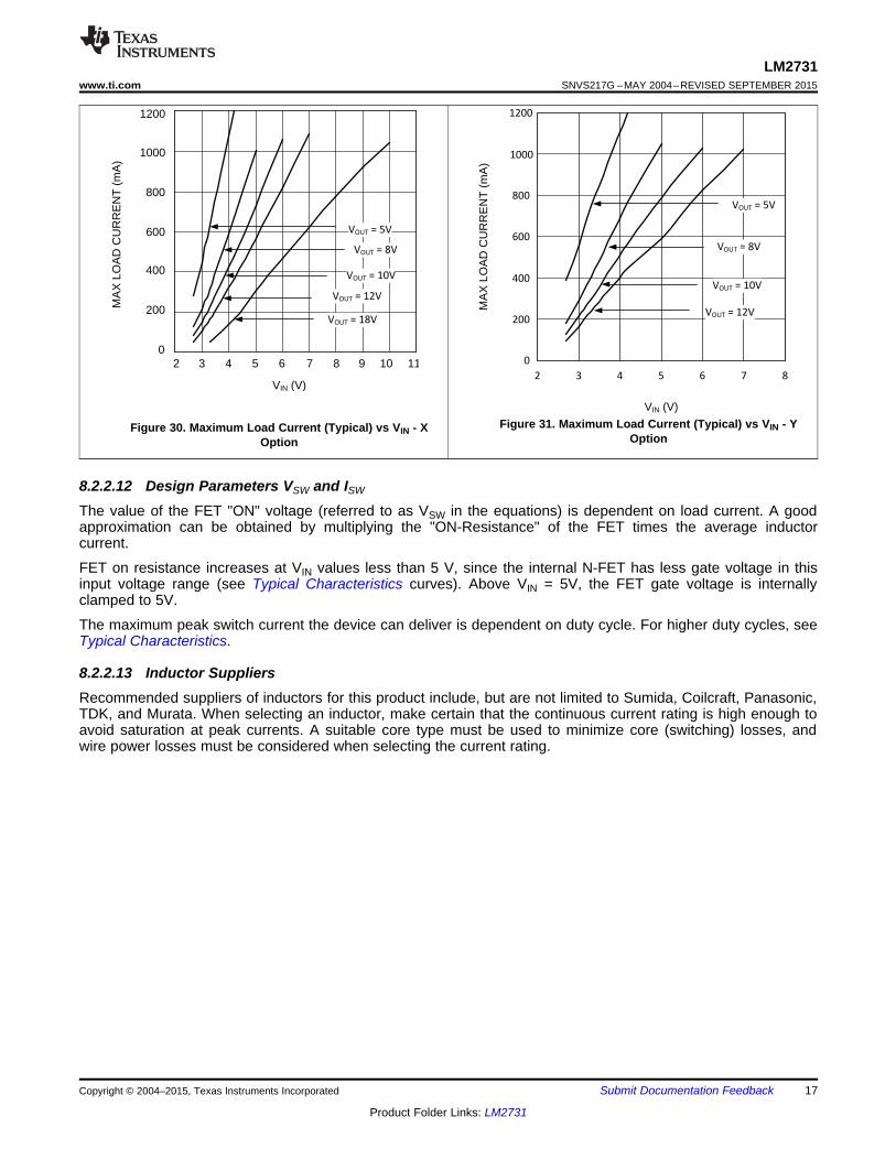
8.2.2.10 Maximum Switch CurrentThe maximum FET switch current available before the current limiter cuts in is dependent on duty cycle of theapplication. This is illustrated in the graphs below which show typical values of switch current for both the "X" and"Y" versions as a function of effective (actual) duty cycle:
Figure 28. Switch Current Limit vs Duty Cycle - X Option Figure 29. Switch Current Limit vs Duty Cycle - Y Option
8.2.2.11 Calculating Load CurrentAs shown in the figure which depicts inductor current, the load current is related to the average inductor currentby the relation:
ILOAD = IIND(AVG) × (1 - DC) (7)
Where "DC" is the duty cycle of the application. The switch current can be found by:ISW = IIND(AVG) + ½ (IRIPPLE) (8)
Inductor ripple current is dependent on inductance, duty cycle, input voltage and frequency:IRIPPLE = DC × (VIN-VSW) / (f × L) (9)
Combining all terms, an expression can be developed which allows the maximum available load current to becalculated:
(10)
The equation shown to calculate maximum load current takes into account the losses in the inductor or turn-OFFswitching losses of the FET and diode. For actual load current in typical applications, we took bench data forvarious input and output voltages for both the "X" and "Y" versions of the LM2731 and displayed the maximumload current available for a typical device in graph form:
16 Submit Documentation Feedback Copyright © 2004–2015, Texas Instruments Incorporated
Product Folder Links: LM2731
2 3 4 5 6 7 8
VIN (V)
0
200
400
600
800
1000
1200
MA
X L
OA
D C
UR
RE
NT
(m
A)
VOUT = 5V
VOUT = 8V
VOUT = 10V
VOUT = 12V
VIN (V)
MA
X L
OA
D C
UR
RE
NT
(m
A)
0
200
400
600
800
1000
1200
2 3 4 5 6 7 8 9 10 11
VOUT = 5V
VOUT = 8V
VOUT = 10V
VOUT = 12V
VOUT = 18V
LM2731www.ti.com SNVS217G –MAY 2004–REVISED SEPTEMBER 2015
Figure 31. Maximum Load Current (Typical) vs VIN - YFigure 30. Maximum Load Current (Typical) vs VIN - XOptionOption
8.2.2.12 Design Parameters VSW and ISW
The value of the FET "ON" voltage (referred to as VSW in the equations) is dependent on load current. A goodapproximation can be obtained by multiplying the "ON-Resistance" of the FET times the average inductorcurrent.
FET on resistance increases at VIN values less than 5 V, since the internal N-FET has less gate voltage in thisinput voltage range (see Typical Characteristics curves). Above VIN = 5V, the FET gate voltage is internallyclamped to 5V.
The maximum peak switch current the device can deliver is dependent on duty cycle. For higher duty cycles, seeTypical Characteristics.
8.2.2.13 Inductor SuppliersRecommended suppliers of inductors for this product include, but are not limited to Sumida, Coilcraft, Panasonic,TDK, and Murata. When selecting an inductor, make certain that the continuous current rating is high enough toavoid saturation at peak currents. A suitable core type must be used to minimize core (switching) losses, andwire power losses must be considered when selecting the current rating.
Copyright © 2004–2015, Texas Instruments Incorporated Submit Documentation Feedback 17
Product Folder Links: LM2731

EF
FIC
IEN
CY
(%
)
LOAD CURRENT (mA)
3.3 -5V Boost
^z_s]v
0 200 400 600 800
70
80
90
100
LM2731 ³<´
SW
FB
GND
VIN
SHDN
U1
R3
51KSHDN
GND
3.3 VIN
C12.2PF R2
13.3K
CF470pF
D1
MBR0520
R1/40.5K
L1/6.8PH
C222PF
5V
OUT
700mA
(TYP)
0 20 40 60 80 100 120 140 160
LOAD (mA)
0
10
20
30
40
50
60
70
80
EF
FIC
IEN
CY
(%
)
7000 100 200 300 400 500 600
LOAD (mA)
EF
FIC
IEN
CY
(%
)
0
10
20
30
40
50
60
70
80
90
100
LM2731SNVS217G –MAY 2004–REVISED SEPTEMBER 2015 www.ti.com
8.2.3 Application CurvesSee Typical Characteristics.
VIN = 3.3 V VOUT = 5 VVIN = 3.3 V VOUT = 12 V
Figure 32. Efficiency vs Load Current - X Option Figure 33. Efficiency vs Load Current - X Option
8.3 System Examples
Figure 34. VIN = 3.3 V, VOUT = 5 V at 700 mA Figure 35. Efficiency vs Load Current
18 Submit Documentation Feedback Copyright © 2004–2015, Texas Instruments Incorporated
Product Folder Links: LM2731

LM2731"Y"
L1 / 1.5 PH
R3
51K
C14.7PF
C24.7PF
R2
120
D1
MBR0520
WHITE
LED's
VIN SW
FB
GNDSHDN
B1LI-ION
3.3 - 4.2V
FLASH
ENABLE
0
- +
EF
FIC
IEN
CY
(%
)
LOAD (mA)
0 50 100 150 200 250
0
10
20
30
40
50
60
70
80
90
100
300
3.3 -9V
^y_s]v
LM2731 ³;´
SW
FB
GND
VIN
SHDN
U1
R3
51KSHDN
GND
3.3 VIN
C12.2PF R2
13.3K
CF330pF
D1
MBR0520
R1/84K
L1/10PH
C24.7PF
D2
D3
D4
D5
R4 R5
9V OUT
240mA (typ)
EF
FIC
IEN
CY
(%
)
LOAD (mA)
0
10
20
30
40
50
60
70
80
90
100
0 50 100 150 200 250
3.3 -12V
Boost
^z_s]v
LM2731 ³<´
SW
FB
GND
VIN
SHDN
U1
R3
51KSHDN
GND
3.3 VIN
C12.2PF R2
13.3K
CF270pF
D1
MBR0520
R1/117K
L1/6.8PH
C210PF
12V
OUT
230mA
(TYP)
LM2731www.ti.com SNVS217G –MAY 2004–REVISED SEPTEMBER 2015
Figure 37. Efficiency vs Load CurrentFigure 36. VIN = 3.3 V, VOUT = 12 V at 230 mA
Figure 39. Efficiency vs Load CurrentFigure 38. VIN = 3.3 V, VOUT = 9 V at 240 mA
Figure 40. White LED Flash Application
Copyright © 2004–2015, Texas Instruments Incorporated Submit Documentation Feedback 19
Product Folder Links: LM2731

LM2731SNVS217G –MAY 2004–REVISED SEPTEMBER 2015 www.ti.com
9 Power Supply RecommendationsThe LM2731 device is designed to operate from various DC power supplies. The impedance of the input supplyrail should be low enough that the input current transient does not cause a drop below SHUTDOWN level. If theinput supply is connected by using long wires, additional bulk capacitance may be required in addition to normalinput capacitor.
10 Layout
10.1 Layout GuidelinesHigh-frequency switching regulators require very careful layout of components to get stable operation and lownoise. All components must be as close as possible to the LM2731 device. TI recommends that a 4-layer PCBbe used so that internal ground planes are available.
As an example, a recommended layout of components is shown in Figure 41.
Some additional guidelines to be observed:• Keep the path between L1, D1, and C2 extremely short. Parasitic trace inductance in series with D1 and C2
will increase noise and ringing.• The feedback components R1, R2 and CF must be kept close to the FB pin of U1 to prevent noise injection
on the FB pin trace.• If internal ground planes are available (recommended), use vias to connect directly to ground at pin 2 of U1,
as well as the negative sides of capacitors C1 and C2.
10.2 Layout Example
Figure 41. Recommended PCB Component Layout
20 Submit Documentation Feedback Copyright © 2004–2015, Texas Instruments Incorporated
Product Folder Links: LM2731

LM2731www.ti.com SNVS217G –MAY 2004–REVISED SEPTEMBER 2015
10.3 Thermal ConsiderationsAt higher duty cycles, the increased ON-time of the FET means the maximum output current will be determinedby power dissipation within the LM2731 FET switch. The switch power dissipation from ON-state conduction iscalculated by:
P(SW) = DC × IIND(AVE)2 × RDS(ON) (11)
There will be some switching losses as well, so some derating needs to be applied when calculating IC powerdissipation.
Copyright © 2004–2015, Texas Instruments Incorporated Submit Documentation Feedback 21
Product Folder Links: LM2731

LM2731SNVS217G –MAY 2004–REVISED SEPTEMBER 2015 www.ti.com
11 Device and Documentation Support
11.1 Device Support
11.1.1 Third-Party Products DisclaimerTI'S PUBLICATION OF INFORMATION REGARDING THIRD-PARTY PRODUCTS OR SERVICES DOES NOTCONSTITUTE AN ENDORSEMENT REGARDING THE SUITABILITY OF SUCH PRODUCTS OR SERVICESOR A WARRANTY, REPRESENTATION OR ENDORSEMENT OF SUCH PRODUCTS OR SERVICES, EITHERALONE OR IN COMBINATION WITH ANY TI PRODUCT OR SERVICE.
11.2 Community ResourcesThe following links connect to TI community resources. Linked contents are provided "AS IS" by the respectivecontributors. They do not constitute TI specifications and do not necessarily reflect TI's views; see TI's Terms ofUse.
TI E2E™ Online Community TI's Engineer-to-Engineer (E2E) Community. Created to foster collaborationamong engineers. At e2e.ti.com, you can ask questions, share knowledge, explore ideas and helpsolve problems with fellow engineers.
Design Support TI's Design Support Quickly find helpful E2E forums along with design support tools andcontact information for technical support.
11.3 TrademarksE2E is a trademark of Texas Instruments.All other trademarks are the property of their respective owners.
11.4 Electrostatic Discharge CautionThese devices have limited built-in ESD protection. The leads should be shorted together or the device placed in conductive foamduring storage or handling to prevent electrostatic damage to the MOS gates.
11.5 GlossarySLYZ022 — TI Glossary.
This glossary lists and explains terms, acronyms, and definitions.
12 Mechanical, Packaging, and Orderable InformationThe following pages include mechanical, packaging, and orderable information. This information is the mostcurrent data available for the designated devices. This data is subject to change without notice and revision ofthis document. For browser-based versions of this data sheet, refer to the left-hand navigation.
22 Submit Documentation Feedback Copyright © 2004–2015, Texas Instruments Incorporated
Product Folder Links: LM2731

PACKAGE OPTION ADDENDUM
www.ti.com 9-Jun-2015
Addendum-Page 1
PACKAGING INFORMATION
Orderable Device Status(1)
Package Type PackageDrawing
Pins PackageQty
Eco Plan(2)
Lead/Ball Finish(6)
MSL Peak Temp(3)
Op Temp (°C) Device Marking(4/5)
Samples
LM2731XMF NRND SOT-23 DBV 5 1000 TBD Call TI Call TI -40 to 125 S51A
LM2731XMF/NOPB ACTIVE SOT-23 DBV 5 1000 Green (RoHS& no Sb/Br)
CU SN Level-1-260C-UNLIM -40 to 125 S51A
LM2731XMFX/NOPB ACTIVE SOT-23 DBV 5 3000 Green (RoHS& no Sb/Br)
CU SN Level-1-260C-UNLIM -40 to 125 S51A
LM2731YMF ACTIVE SOT-23 DBV 5 1000 TBD Call TI Call TI -40 to 125 S51B
LM2731YMF/NOPB ACTIVE SOT-23 DBV 5 1000 Green (RoHS& no Sb/Br)
CU SN Level-1-260C-UNLIM -40 to 125 S51B
LM2731YMFX/NOPB ACTIVE SOT-23 DBV 5 3000 Green (RoHS& no Sb/Br)
CU SN Level-1-260C-UNLIM -40 to 125 S51B
(1) The marketing status values are defined as follows:ACTIVE: Product device recommended for new designs.LIFEBUY: TI has announced that the device will be discontinued, and a lifetime-buy period is in effect.NRND: Not recommended for new designs. Device is in production to support existing customers, but TI does not recommend using this part in a new design.PREVIEW: Device has been announced but is not in production. Samples may or may not be available.OBSOLETE: TI has discontinued the production of the device.
(2) Eco Plan - The planned eco-friendly classification: Pb-Free (RoHS), Pb-Free (RoHS Exempt), or Green (RoHS & no Sb/Br) - please check http://www.ti.com/productcontent for the latest availabilityinformation and additional product content details.TBD: The Pb-Free/Green conversion plan has not been defined.Pb-Free (RoHS): TI's terms "Lead-Free" or "Pb-Free" mean semiconductor products that are compatible with the current RoHS requirements for all 6 substances, including the requirement thatlead not exceed 0.1% by weight in homogeneous materials. Where designed to be soldered at high temperatures, TI Pb-Free products are suitable for use in specified lead-free processes.Pb-Free (RoHS Exempt): This component has a RoHS exemption for either 1) lead-based flip-chip solder bumps used between the die and package, or 2) lead-based die adhesive used betweenthe die and leadframe. The component is otherwise considered Pb-Free (RoHS compatible) as defined above.Green (RoHS & no Sb/Br): TI defines "Green" to mean Pb-Free (RoHS compatible), and free of Bromine (Br) and Antimony (Sb) based flame retardants (Br or Sb do not exceed 0.1% by weightin homogeneous material)
(3) MSL, Peak Temp. - The Moisture Sensitivity Level rating according to the JEDEC industry standard classifications, and peak solder temperature.
(4) There may be additional marking, which relates to the logo, the lot trace code information, or the environmental category on the device.
(5) Multiple Device Markings will be inside parentheses. Only one Device Marking contained in parentheses and separated by a "~" will appear on a device. If a line is indented then it is a continuationof the previous line and the two combined represent the entire Device Marking for that device.

PACKAGE OPTION ADDENDUM
www.ti.com 9-Jun-2015
Addendum-Page 2
(6) Lead/Ball Finish - Orderable Devices may have multiple material finish options. Finish options are separated by a vertical ruled line. Lead/Ball Finish values may wrap to two lines if the finishvalue exceeds the maximum column width.
Important Information and Disclaimer:The information provided on this page represents TI's knowledge and belief as of the date that it is provided. TI bases its knowledge and belief on informationprovided by third parties, and makes no representation or warranty as to the accuracy of such information. Efforts are underway to better integrate information from third parties. TI has taken andcontinues to take reasonable steps to provide representative and accurate information but may not have conducted destructive testing or chemical analysis on incoming materials and chemicals.TI and TI suppliers consider certain information to be proprietary, and thus CAS numbers and other limited information may not be available for release.
In no event shall TI's liability arising out of such information exceed the total purchase price of the TI part(s) at issue in this document sold by TI to Customer on an annual basis.

TAPE AND REEL INFORMATION
*All dimensions are nominal
Device PackageType
PackageDrawing
Pins SPQ ReelDiameter
(mm)
ReelWidth
W1 (mm)
A0(mm)
B0(mm)
K0(mm)
P1(mm)
W(mm)
Pin1Quadrant
LM2731XMF SOT-23 DBV 5 1000 178.0 8.4 3.2 3.2 1.4 4.0 8.0 Q3
LM2731XMF/NOPB SOT-23 DBV 5 1000 178.0 8.4 3.2 3.2 1.4 4.0 8.0 Q3
LM2731XMFX/NOPB SOT-23 DBV 5 3000 178.0 8.4 3.2 3.2 1.4 4.0 8.0 Q3
LM2731YMF SOT-23 DBV 5 1000 178.0 8.4 3.2 3.2 1.4 4.0 8.0 Q3
LM2731YMF/NOPB SOT-23 DBV 5 1000 178.0 8.4 3.2 3.2 1.4 4.0 8.0 Q3
LM2731YMFX/NOPB SOT-23 DBV 5 3000 178.0 8.4 3.2 3.2 1.4 4.0 8.0 Q3
PACKAGE MATERIALS INFORMATION
www.ti.com 20-Dec-2016
Pack Materials-Page 1
*All dimensions are nominal
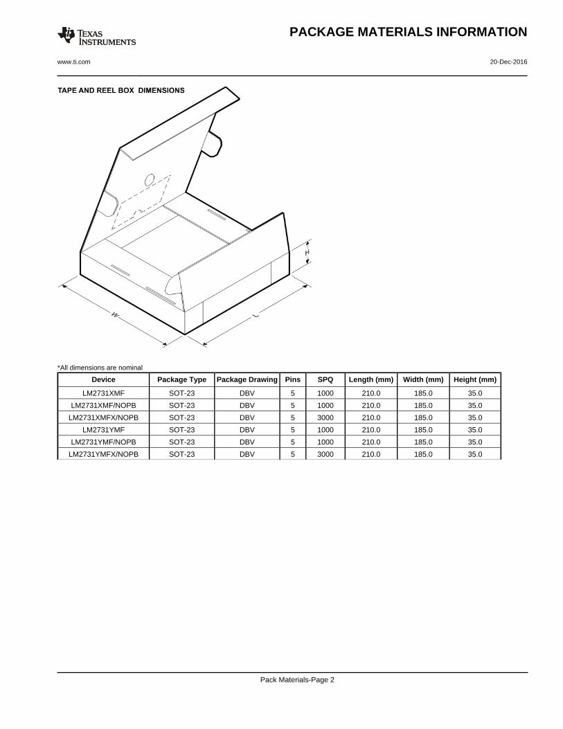
Device Package Type Package Drawing Pins SPQ Length (mm) Width (mm) Height (mm)
LM2731XMF SOT-23 DBV 5 1000 210.0 185.0 35.0
LM2731XMF/NOPB SOT-23 DBV 5 1000 210.0 185.0 35.0
LM2731XMFX/NOPB SOT-23 DBV 5 3000 210.0 185.0 35.0
LM2731YMF SOT-23 DBV 5 1000 210.0 185.0 35.0
LM2731YMF/NOPB SOT-23 DBV 5 1000 210.0 185.0 35.0
LM2731YMFX/NOPB SOT-23 DBV 5 3000 210.0 185.0 35.0
PACKAGE MATERIALS INFORMATION
www.ti.com 20-Dec-2016
Pack Materials-Page 2


www.ti.com
PACKAGE OUTLINE
C
TYP0.220.08
0.25
3.02.6
2X 0.95
1.9
1.45 MAX
TYP0.150.00
5X 0.50.3
TYP0.60.3
TYP80
1.9
A
3.052.75
B1.751.45
(1.1)
SOT-23 - 1.45 mm max heightDBV0005ASMALL OUTLINE TRANSISTOR
4214839/C 04/2017
NOTES: 1. All linear dimensions are in millimeters. Any dimensions in parenthesis are for reference only. Dimensioning and tolerancing per ASME Y14.5M.2. This drawing is subject to change without notice.3. Refernce JEDEC MO-178.
0.2 C A B
1
34
5
2
INDEX AREAPIN 1
GAGE PLANE
SEATING PLANE
0.1 C
SCALE 4.000

www.ti.com
EXAMPLE BOARD LAYOUT
0.07 MAXARROUND
0.07 MINARROUND
5X (1.1)
5X (0.6)
(2.6)
(1.9)
2X (0.95)
(R0.05) TYP
4214839/C 04/2017
SOT-23 - 1.45 mm max heightDBV0005ASMALL OUTLINE TRANSISTOR
NOTES: (continued) 4. Publication IPC-7351 may have alternate designs. 5. Solder mask tolerances between and around signal pads can vary based on board fabrication site.
SYMM
LAND PATTERN EXAMPLEEXPOSED METAL SHOWN
SCALE:15X
PKG
1
3 4
5
2
SOLDER MASKOPENINGMETAL UNDER
SOLDER MASK
SOLDER MASKDEFINED
EXPOSED METAL
METALSOLDER MASKOPENING
NON SOLDER MASKDEFINED
(PREFERRED)
SOLDER MASK DETAILS
EXPOSED METAL

www.ti.com
EXAMPLE STENCIL DESIGN
(2.6)
(1.9)
2X(0.95)
5X (1.1)
5X (0.6)
(R0.05) TYP
SOT-23 - 1.45 mm max heightDBV0005ASMALL OUTLINE TRANSISTOR
4214839/C 04/2017
NOTES: (continued) 6. Laser cutting apertures with trapezoidal walls and rounded corners may offer better paste release. IPC-7525 may have alternate design recommendations. 7. Board assembly site may have different recommendations for stencil design.
SOLDER PASTE EXAMPLEBASED ON 0.125 mm THICK STENCIL
SCALE:15X
SYMM
PKG
1
3 4
5
2

IMPORTANT NOTICE
Texas Instruments Incorporated (TI) reserves the right to make corrections, enhancements, improvements and other changes to itssemiconductor products and services per JESD46, latest issue, and to discontinue any product or service per JESD48, latest issue. Buyersshould obtain the latest relevant information before placing orders and should verify that such information is current and complete.TI’s published terms of sale for semiconductor products (http://www.ti.com/sc/docs/stdterms.htm) apply to the sale of packaged integratedcircuit products that TI has qualified and released to market. Additional terms may apply to the use or sale of other types of TI products andservices.Reproduction of significant portions of TI information in TI data sheets is permissible only if reproduction is without alteration and isaccompanied by all associated warranties, conditions, limitations, and notices. TI is not responsible or liable for such reproduceddocumentation. Information of third parties may be subject to additional restrictions. Resale of TI products or services with statementsdifferent from or beyond the parameters stated by TI for that product or service voids all express and any implied warranties for theassociated TI product or service and is an unfair and deceptive business practice. TI is not responsible or liable for any such statements.Buyers and others who are developing systems that incorporate TI products (collectively, “Designers”) understand and agree that Designersremain responsible for using their independent analysis, evaluation and judgment in designing their applications and that Designers havefull and exclusive responsibility to assure the safety of Designers' applications and compliance of their applications (and of all TI productsused in or for Designers’ applications) with all applicable regulations, laws and other applicable requirements. Designer represents that, withrespect to their applications, Designer has all the necessary expertise to create and implement safeguards that (1) anticipate dangerousconsequences of failures, (2) monitor failures and their consequences, and (3) lessen the likelihood of failures that might cause harm andtake appropriate actions. Designer agrees that prior to using or distributing any applications that include TI products, Designer willthoroughly test such applications and the functionality of such TI products as used in such applications.TI’s provision of technical, application or other design advice, quality characterization, reliability data or other services or information,including, but not limited to, reference designs and materials relating to evaluation modules, (collectively, “TI Resources”) are intended toassist designers who are developing applications that incorporate TI products; by downloading, accessing or using TI Resources in anyway, Designer (individually or, if Designer is acting on behalf of a company, Designer’s company) agrees to use any particular TI Resourcesolely for this purpose and subject to the terms of this Notice.TI’s provision of TI Resources does not expand or otherwise alter TI’s applicable published warranties or warranty disclaimers for TIproducts, and no additional obligations or liabilities arise from TI providing such TI Resources. TI reserves the right to make corrections,enhancements, improvements and other changes to its TI Resources. TI has not conducted any testing other than that specificallydescribed in the published documentation for a particular TI Resource.Designer is authorized to use, copy and modify any individual TI Resource only in connection with the development of applications thatinclude the TI product(s) identified in such TI Resource. NO OTHER LICENSE, EXPRESS OR IMPLIED, BY ESTOPPEL OR OTHERWISETO ANY OTHER TI INTELLECTUAL PROPERTY RIGHT, AND NO LICENSE TO ANY TECHNOLOGY OR INTELLECTUAL PROPERTYRIGHT OF TI OR ANY THIRD PARTY IS GRANTED HEREIN, including but not limited to any patent right, copyright, mask work right, orother intellectual property right relating to any combination, machine, or process in which TI products or services are used. Informationregarding or referencing third-party products or services does not constitute a license to use such products or services, or a warranty orendorsement thereof. Use of TI Resources may require a license from a third party under the patents or other intellectual property of thethird party, or a license from TI under the patents or other intellectual property of TI.TI RESOURCES ARE PROVIDED “AS IS” AND WITH ALL FAULTS. TI DISCLAIMS ALL OTHER WARRANTIES ORREPRESENTATIONS, EXPRESS OR IMPLIED, REGARDING RESOURCES OR USE THEREOF, INCLUDING BUT NOT LIMITED TOACCURACY OR COMPLETENESS, TITLE, ANY EPIDEMIC FAILURE WARRANTY AND ANY IMPLIED WARRANTIES OFMERCHANTABILITY, FITNESS FOR A PARTICULAR PURPOSE, AND NON-INFRINGEMENT OF ANY THIRD PARTY INTELLECTUALPROPERTY RIGHTS. TI SHALL NOT BE LIABLE FOR AND SHALL NOT DEFEND OR INDEMNIFY DESIGNER AGAINST ANY CLAIM,INCLUDING BUT NOT LIMITED TO ANY INFRINGEMENT CLAIM THAT RELATES TO OR IS BASED ON ANY COMBINATION OFPRODUCTS EVEN IF DESCRIBED IN TI RESOURCES OR OTHERWISE. IN NO EVENT SHALL TI BE LIABLE FOR ANY ACTUAL,DIRECT, SPECIAL, COLLATERAL, INDIRECT, PUNITIVE, INCIDENTAL, CONSEQUENTIAL OR EXEMPLARY DAMAGES INCONNECTION WITH OR ARISING OUT OF TI RESOURCES OR USE THEREOF, AND REGARDLESS OF WHETHER TI HAS BEENADVISED OF THE POSSIBILITY OF SUCH DAMAGES.Unless TI has explicitly designated an individual product as meeting the requirements of a particular industry standard (e.g., ISO/TS 16949and ISO 26262), TI is not responsible for any failure to meet such industry standard requirements.Where TI specifically promotes products as facilitating functional safety or as compliant with industry functional safety standards, suchproducts are intended to help enable customers to design and create their own applications that meet applicable functional safety standardsand requirements. Using products in an application does not by itself establish any safety features in the application. Designers mustensure compliance with safety-related requirements and standards applicable to their applications. Designer may not use any TI products inlife-critical medical equipment unless authorized officers of the parties have executed a special contract specifically governing such use.Life-critical medical equipment is medical equipment where failure of such equipment would cause serious bodily injury or death (e.g., lifesupport, pacemakers, defibrillators, heart pumps, neurostimulators, and implantables). Such equipment includes, without limitation, allmedical devices identified by the U.S. Food and Drug Administration as Class III devices and equivalent classifications outside the U.S.TI may expressly designate certain products as completing a particular qualification (e.g., Q100, Military Grade, or Enhanced Product).Designers agree that it has the necessary expertise to select the product with the appropriate qualification designation for their applicationsand that proper product selection is at Designers’ own risk. Designers are solely responsible for compliance with all legal and regulatoryrequirements in connection with such selection.Designer will fully indemnify TI and its representatives against any damages, costs, losses, and/or liabilities arising out of Designer’s non-compliance with the terms and provisions of this Notice.
Mailing Address: Texas Instruments, Post Office Box 655303, Dallas, Texas 75265Copyright © 2018, Texas Instruments Incorporated