
LM25576 42-V, 3-A Step-Down Switching Regulator datasheet ... · BST SW COMP FB SS RAMP RT VCC VIN...
35
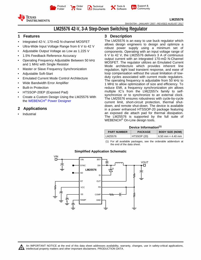
BST SW COMP FB SS RAMP RT VCC VIN OUT IS GND LM25576 VIN VOUT SYNC SD Product Folder Order Now Technical Documents Tools & Software Support & Community An IMPORTANT NOTICE at the end of this data sheet addresses availability, warranty, changes, use in safety-critical applications, intellectual property matters and other important disclaimers. PRODUCTION DATA. LM25576 SNVS470H – JANUARY 2007 – REVISED AUGUST 2017 LM25576 42-V, 3-A Step-Down Switching Regulator 1 1 Features 1• Integrated 42-V, 170-mΩ N-channel MOSFET • Ultra-Wide Input Voltage Range from 6 V to 42 V • Adjustable Output Voltage as Low as 1.225 V • 1.5% Feedback Reference Accuracy • Operating Frequency Adjustable Between 50 kHz and 1 MHz with Single Resistor • Master or Slave Frequency Synchronization • Adjustable Soft-Start • Emulated Current Mode Control Architecture • Wide Bandwidth Error Amplifier • Built-in Protection • HTSSOP-20EP (Exposed Pad) • Create a Custom Design Using the LM25576 With the WEBENCH ® Power Designer 2 Applications • Industrial 3 Description The LM25576 is an easy to use buck regulator which allows design engineers to design and optimize a robust power supply using a minimum set of components. Operating with an input voltage range of 6 V to 42 V, the LM25576 delivers 3 A of continuous output current with an integrated 170-mΩ N-Channel MOSFET. The regulator utilizes an Emulated Current Mode architecture which provides inherent line regulation, tight load transient response, and ease of loop compensation without the usual limitation of low- duty cycles associated with current mode regulators. The operating frequency is adjustable from 50 kHz to 1 MHz to allow optimization of size and efficiency. To reduce EMI, a frequency synchronization pin allows multiple IC’s from the LM(2)557x family to self- synchronize or to synchronize to an external clock. The LM25576 ensures robustness with cycle-by-cycle current limit, short-circuit protection, thermal shut- down, and remote shut-down. The device is available in a power enhanced HTSSOP-20 package featuring an exposed die attach pad for thermal dissipation. The LM25576 is supported by the full suite of WEBENCH ® On-Line design tools. Device Information (1) PART NUMBER PACKAGE BODY SIZE (NOM) LM25576 HTSSOP (20) 6.50 mm × 4.40 mm (1) For all available packages, see the orderable addendum at the end of the data sheet. Simplified Application Schematic
Transcript of LM25576 42-V, 3-A Step-Down Switching Regulator datasheet ... · BST SW COMP FB SS RAMP RT VCC VIN...
BST
SW
COMP
FB
SS
RAMP
RT
VCC
VIN
OUT
IS
GND
LM25576
VIN
VOUT
SYNC
SD
Product
Folder
Order
Now
Technical
Documents
Tools &
Software
Support &Community
An IMPORTANT NOTICE at the end of this data sheet addresses availability, warranty, changes, use in safety-critical applications,intellectual property matters and other important disclaimers. PRODUCTION DATA.
LM25576SNVS470H –JANUARY 2007–REVISED AUGUST 2017
LM25576 42-V, 3-A Step-Down Switching Regulator
1
1 Features1• Integrated 42-V, 170-mΩ N-channel MOSFET• Ultra-Wide Input Voltage Range from 6 V to 42 V• Adjustable Output Voltage as Low as 1.225 V• 1.5% Feedback Reference Accuracy• Operating Frequency Adjustable Between 50 kHz
and 1 MHz with Single Resistor• Master or Slave Frequency Synchronization• Adjustable Soft-Start• Emulated Current Mode Control Architecture• Wide Bandwidth Error Amplifier• Built-in Protection• HTSSOP-20EP (Exposed Pad)• Create a Custom Design Using the LM25576 With
the WEBENCH® Power Designer
2 Applications• Industrial
3 DescriptionThe LM25576 is an easy to use buck regulator whichallows design engineers to design and optimize arobust power supply using a minimum set ofcomponents. Operating with an input voltage range of6 V to 42 V, the LM25576 delivers 3 A of continuousoutput current with an integrated 170-mΩ N-ChannelMOSFET. The regulator utilizes an Emulated CurrentMode architecture which provides inherent lineregulation, tight load transient response, and ease ofloop compensation without the usual limitation of low-duty cycles associated with current mode regulators.The operating frequency is adjustable from 50 kHz to1 MHz to allow optimization of size and efficiency. Toreduce EMI, a frequency synchronization pin allowsmultiple IC’s from the LM(2)557x family to self-synchronize or to synchronize to an external clock.The LM25576 ensures robustness with cycle-by-cyclecurrent limit, short-circuit protection, thermal shut-down, and remote shut-down. The device is availablein a power enhanced HTSSOP-20 package featuringan exposed die attach pad for thermal dissipation.The LM25576 is supported by the full suite ofWEBENCH® On-Line design tools.
Device Information(1)
PART NUMBER PACKAGE BODY SIZE (NOM)LM25576 HTSSOP (20) 6.50 mm × 4.40 mm
(1) For all available packages, see the orderable addendum atthe end of the data sheet.
Simplified Application Schematic
2
LM25576SNVS470H –JANUARY 2007–REVISED AUGUST 2017 www.ti.com
Product Folder Links: LM25576
Submit Documentation Feedback Copyright © 2007–2017, Texas Instruments Incorporated
Table of Contents1 Features .................................................................. 12 Applications ........................................................... 13 Description ............................................................. 14 Revision History..................................................... 25 Pin Configuration and Functions ......................... 36 Specifications......................................................... 5
6.1 Absolute Maximum Ratings ...................................... 56.2 ESD Ratings ............................................................ 56.3 Recommended Operating Conditions....................... 56.4 Electrical Characteristics........................................... 66.5 Typical Characteristics .............................................. 7
7 Detailed Description ............................................ 107.1 Overview ................................................................. 107.2 Functional Block Diagram ....................................... 107.3 Feature Description................................................. 10
7.4 Device Functional Modes........................................ 118 Application and Implementation ........................ 17
8.1 Application Information............................................ 178.2 Typical Application .................................................. 24
9 Layout ................................................................... 259.1 Layout Guidelines ................................................... 259.2 Layout Example ...................................................... 26
10 Device and Documentation Support ................. 2810.1 Device Support...................................................... 2810.2 Receiving Notification of Documentation Updates 2810.3 Community Resources.......................................... 2810.4 Trademarks ........................................................... 2810.5 Electrostatic Discharge Caution............................ 2810.6 Glossary ................................................................ 28
11 Mechanical, Packaging, and OrderableInformation ........................................................... 29
4 Revision HistoryNOTE: Page numbers for previous revisions may differ from page numbers in the current version.
Changes from Revision F (March 2009) to Revision G Page
• Changed layout of National Data Sheet to TI format ............................................................................................................ 1
Changes from Revision G (April 2013) to Revision H Page
• Added Application and Implementation section, Device Information table, Pin Configuration and Functions section,ESD Ratings table, Thermal Information table, Feature Description section, Device Functional Modes, Device andDocumentation Support section, and Mechanical, Packaging, and Orderable Information section....................................... 1

1
2
3
4
5
6
7
8
9
10
VIN
PRE
COMP
VCC
SW
PGND
IS
RT
SS11
12
13
14
15
16
RAMP
SYNC
OUT
SD
BST
AGND
FB
17
18
19
20
PGND
IS
VIN
SW
3
LM25576www.ti.com SNVS470H –JANUARY 2007–REVISED AUGUST 2017
Product Folder Links: LM25576
Submit Documentation FeedbackCopyright © 2007–2017, Texas Instruments Incorporated
5 Pin Configuration and Functions
PWP20-HTSSOP
Top View
Pin FunctionsNO. NAME DESCRIPTION
1 VCC
Output of the bias regulatorVcc tracks Vin up to 9 V. Beyond 9 V, Vcc is regulated to 7 Volts. A 0.1 uF to 1 uF ceramic decouplingcapacitor is required. An external voltage (7.5 V – 14 V) can be applied to this pin to reduce internal powerdissipation.
2 SD
Shutdown or UVLO inputIf the SD pin voltage is below 0.7 V the regulator will be in a low power state. If the SD pin voltage is between0.7 V and 1.225 V the regulator will be in standby mode. If the SD pin voltage is above 1.225 V the regulatorwill be operational. An external voltage divider can be used to set a line undervoltage shutdown threshold. Ifthe SD pin is left open circuit, a 5 µA pull-up current source configures the regulator fully operational.
3, 4 VIN Input supply voltageNominal operating range: 6 V to 42 V
5 SYNCOscillator synchronization input or outputThe internal oscillator can be synchronized to an external clock with an external pull-down device. MultipleLM25576 devices can be synchronized together by connection of their SYNC pins.
6 COMP Output of the internal error amplifierThe loop compensation network should be connected between this pin and the FB pin.
7 FB Feedback signal from the regulated outputThis pin is connected to the inverting input of the internal error amplifier. The regulation threshold is 1.225 V.
8 RT Internal oscillator frequency set inputThe internal oscillator is set with a single resistor, connected between this pin and the AGND pin.
9 RAMPRamp control signalAn external capacitor connected between this pin and the AGND pin sets the ramp slope used for currentmode control. Recommended capacitor range 50 pF to 2000 pF.
10 AGND Analog groundInternal reference for the regulator control functions
11 SSSoft-startAn external capacitor and an internal 10 µA current source set the time constant for the rise of the error ampreference. The SS pin is held low during standby, Vcc UVLO and thermal shutdown.
12 OUT Output voltage connectionConnect directly to the regulated output voltage.
13, 14 PGND Power groundLow side reference for the PRE switch and the IS sense resistor.
15, 16 IS
Current senseCurrent measurement connection for the re-circulating diode. An internal sense resistor and a sample/holdcircuit sense the diode current near the conclusion of the off-time. This current measurement provides the DClevel of the emulated current ramp.

4
LM25576SNVS470H –JANUARY 2007–REVISED AUGUST 2017 www.ti.com
Product Folder Links: LM25576
Submit Documentation Feedback Copyright © 2007–2017, Texas Instruments Incorporated
Pin Functions (continued)NO. NAME DESCRIPTION
17, 18 SWSwitching nodeThe source terminal of the internal buck switch. The SW pin should be connected to the external Schottkydiode and to the buck inductor.
19 PRE
Pre-charge assist for the bootstrap capacitorThis open drain output can be connected to SW pin to aid charging the bootstrap capacitor during very lightload conditions or in applications where the output may be pre-charged before the LM25576 is enabled. Aninternal pre-charge MOSFET is turned on for 265 ns each cycle just prior to the on-time interval of the buckswitch.
20 BSTBoost input for bootstrap capacitorAn external capacitor is required between the BST and the SW pins. A 0.022 µF ceramic capacitor isrecommended. The capacitor is charged from Vcc via an internal diode during the off-time of the buck switch.
NA EPExposed PadExposed metal pad on the underside of the device. It is recommended to connect this pad to the PWB groundplane, in order to aid in heat dissipation.

5
LM25576www.ti.com SNVS470H –JANUARY 2007–REVISED AUGUST 2017
Product Folder Links: LM25576
Submit Documentation FeedbackCopyright © 2007–2017, Texas Instruments Incorporated
(1) Stresses beyond those listed under Absolute Maximum Ratings may cause permanent damage to the device. These are stress ratingsonly, which do not imply functional operation of the device at these or any other conditions beyond those indicated under RecommendedOperating Conditions. Exposure to absolute-maximum-rated conditions for extended periods may affect device reliability.
(2) If Military/Aerospace specified devices are required, please contact the Texas Instruments Sales Office/Distributors for availability andspecifications.
6 Specifications
6.1 Absolute Maximum Ratingsover operating free-air temperature range (unless otherwise noted) (1) (2)
MIN MAX UNITVIN to GND 45 VBST to GND 60 VPRE to GND 45 VSW to GND (Steady State) –1.5 VBST to VCC 45 VSD, VCC to GND 14 VBST to SW 14 VOUT to GND Limited Vin VSYNC, SS, FB, RAMP to GND 7 VStorage temperature, Tstg –65 150 °C
(1) JEDEC document JEP155 states that 500-V HBM allows safe manufacturing with a standard ESD control process.
6.2 ESD RatingsVALUE UNIT
V(ESD) Electrostatic discharge Human-body model (HBM), per ANSI/ESDA/JEDEC JS-001 (1) ±2 kV
(1) Absolute Maximum Ratings are limits beyond which damage to the device may occur. Operating Ratings are conditions under whichoperation of the device is intended to be functional. For ensured specifications and test conditions, see the Electrical Characteristics.
6.3 Recommended Operating Conditions (1)
MIN MAX UNITVIN 6 42 VTJ Operation junction temperature –40 125 °C

6
LM25576SNVS470H –JANUARY 2007–REVISED AUGUST 2017 www.ti.com
Product Folder Links: LM25576
Submit Documentation Feedback Copyright © 2007–2017, Texas Instruments Incorporated
(1) Min and Max limits are 100% production tested at 25°C. Limits over the operating temperature range are ensured through correlationusing Statistical Quality Control (SQC) methods. Limits are used to calculate Texas Instruments' Average Outgoing Quality Level(AOQL).
6.4 Electrical Characteristicsat TJ = 25°C, and VIN = 24 V, RT = 32.4 kΩ (unless otherwise noted). (1)
PARAMETER TEST CONDITIONS MIN TYP MAX UNITSTARTUP REGULATORVccReg Vcc Regulator Output TJ = –40°C to +125°C 6.85 7.15 7.45 V
Vcc LDO Mode turn-off 9 VVcc Current Limit Vcc = 0 V 25 mA
VCC SUPPLYVcc UVLO Threshold (Vcc increasing) TJ = –40°C to +125°C 5.03 5.35 5.67 VVcc Undervoltage Hysteresis 0.35 VBias Current (Iin) FB = 1.3 V TJ = –40°C to +125°C 3.7 4.5 mAShutdown Current (Iin) SD = 0 V TJ = –40°C to +125°C 48 70 µA
SHUTDOWN THRESHOLDSShutdown Threshold (SD Increasing) TJ = –40°C to +125°C 0.47 0.7 0.9 VShutdown Hysteresis 0.1 VStandby Threshold (Standby Increasing) TJ = –40°C to +125°C 1.17 1.225 1.28 VStandby Hysteresis 0.1 VSD Pull-up Current Source 5 µA
SWITCH CHARACTERSICSBuck Switch Rds(on) TJ = –40°C to +125°C 330 660 mΩBOOST UVLO 4 VBOOST UVLO Hysteresis 0.56 VPre-charge Switch Rds(on) 70 ΩPre-charge Switch on-time 250 ns
CURRENT LIMITCycle by Cycle Current Limit RAMP = 0 V TJ = –40°C to +125°C 1.8 2.1 2.5 ACycle by Cycle Current Limit Delay RAMP = 2.5 V 85 ns
SOFT-STARTSS Current Source TJ = –40°C to +125°C 7 10 14 µA
OSCILLATORFrequency1 TJ = –40°C to +125°C 180 200 220 kHzFrequency2 RT = 11 kΩ TJ = –40°C to +125°C 425 485 545 kHzSYNC Source Impedance 11 kΩSYNC Sink Impedance 110 ΩSYNC Threshold (falling) 1.3 VSYNC Frequency RT = 11 kΩ TJ = –40°C to +125°C 550 kHzSYNC Pulse Width Minimum TJ = –40°C to +125°C 15 ns
RAMP GENERATOR
Ramp Current 1 Vin = 36 V,Vout=10 V TJ = –40°C to +125°C 272 310 368 µA
Ramp Current 2 Vin = 10 V,Vout=10 V TJ = –40°C to +125°C 36 50 64 µA
PWM COMPARATORForced Off-time TJ = –40°C to +125°C 416 500 575 nsMin On-time 80 nsCOMP to PWM Comparator Offset 0.7 V

TEMPERATURE (oC)
NO
RM
ALI
ZE
D O
SC
ILLA
TO
R F
RE
QU
EN
CY
-50 -25 0 25 50 75 100 1250.990
0.995
1.000
1.005
1.010
RT (k:)
OS
CIL
LAT
OR
FR
EQ
UE
NC
Y (
kHz)
1 10 100 100010
100
1000
7
LM25576www.ti.com SNVS470H –JANUARY 2007–REVISED AUGUST 2017
Product Folder Links: LM25576
Submit Documentation FeedbackCopyright © 2007–2017, Texas Instruments Incorporated
Electrical Characteristics (continued)at TJ = 25°C, and VIN = 24 V, RT = 32.4 kΩ (unless otherwise noted).(1)
PARAMETER TEST CONDITIONS MIN TYP MAX UNITERROR AMPLIFIER
Feedback Voltage Vfb = COMP TJ = –40°C to +125°C 1.207 1.225 1.243 VFB Bias Current 17 nADC Gain 70 dBCOMP Sink / Source Current TJ = –40°C to +125°C 3 mAUnity Gain Bandwidth 3 MHz
DIODE SENSE RESISTANCEDSENSE 83 mΩTHERMAL SHUTDOWN
TsdThermal Shutdown Threshold 165 °CThermal Shutdown Hysteresis 25 °C
6.5 Typical Characteristics
Figure 1. Oscillator Frequency vs RT
FOSC = 200kHz
Figure 2. Oscillator Frequency vs Temperature

0 2 4 6 8 100
2
4
6
8
10
VC
C (
V)
VIN (V)
Ramp Up
Ramp Down PH
AS
E (
°)
10k 100k 1M 10M 100M
FREQUENCY (Hz)
-30
-20
-10
0
10
20
30
40
50G
AIN
(dB
)
-135
-90
-45
0
45
90
135
180
225
GAIN
PHASE
TEMPERATURE (oC)
NO
RM
ALI
ZE
D S
OF
TS
TA
RT
CU
RR
EN
T
-50 -25 0 25 50 75 100 1250.90
0.95
1.00
1.05
1.10
0 4 16 20 24
ICC (mA)
0
2
4
6
8
VC
C (
V)
8 12
8
LM25576SNVS470H –JANUARY 2007–REVISED AUGUST 2017 www.ti.com
Product Folder Links: LM25576
Submit Documentation Feedback Copyright © 2007–2017, Texas Instruments Incorporated
Typical Characteristics (continued)
Figure 3. Soft Start Current vs Temperature
VIN = 12V
Figure 4. VCC vs ICC
RL = 7 kΩ
Figure 5. VCC vs VIN
AVCL = 101
Figure 6. Error Amplifier Gain and Phase

0.5 1 1.5 2 2.5 30
10
20
30
40
50
60
70
80
90
100
EF
FIC
IEN
CY
(%
)
IOUT (A)
VIN = 24V
VIN = 7V
9
LM25576www.ti.com SNVS470H –JANUARY 2007–REVISED AUGUST 2017
Product Folder Links: LM25576
Submit Documentation FeedbackCopyright © 2007–2017, Texas Instruments Incorporated
Typical Characteristics (continued)
Figure 7. Demoboard Efficiency vs IOUT and VIN
FB
SW
RT
VIN
BSTSD
5VS
R
Q
Q
AGND
IS
CLK
+
SS
PRE
3, 4
2
11
7
6
5 8 9 12
10
13, 14
1
SD
Ir
LM25576
SHUTDOWN
STANDBY
7VREGULATOR
SYNC
SYNC
OSCILLATOR
RAMP OUT
PGND
CLK
CLKCOMP
ERRORAMP
R321k
C3330p
C11330p
R710
C922
C10150
R61.65k
R55.11k
L133 PH
C70.022
C80.47
D1CSHD6-60C
15, 16
19
17, 18
20
THERMALSHUTDOWNUVLO
UVLO
CLK
DIS
VCC
LEVELSHIFT
DRIVER
1.225V
1.225V
0.7V
0.7V
R449.9k
C50.01C6
open
R2OPEN
C12OPEN
C40.01
C22.2
C12.2
R1OPEN
7V ± 42V VIN
VIN
2.1V
PWM
C_LIMIT
10 PA
5 PA
VIN
TRACKSAMPLE
andHOLD
0.5V/A
RAMP GENERATORIr = (5 PA x (VIN ± VOUT))
+ 25 PA
10
LM25576SNVS470H –JANUARY 2007–REVISED AUGUST 2017 www.ti.com
Product Folder Links: LM25576
Submit Documentation Feedback Copyright © 2007–2017, Texas Instruments Incorporated
7 Detailed Description
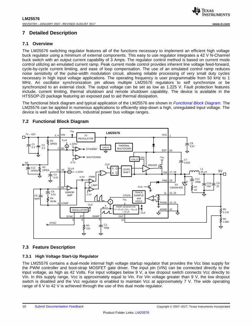
7.1 OverviewThe LM25576 switching regulator features all of the functions necessary to implement an efficient high voltagebuck regulator using a minimum of external components. This easy to use regulator integrates a 42 V N-Channelbuck switch with an output current capability of 3 Amps. The regulator control method is based on current modecontrol utilizing an emulated current ramp. Peak current mode control provides inherent line voltage feed-forward,cycle-by-cycle current limiting, and ease of loop compensation. The use of an emulated control ramp reducesnoise sensitivity of the pulse-width modulation circuit, allowing reliable processing of very small duty cyclesnecessary in high input voltage applications. The operating frequency is user programmable from 50 kHz to 1MHz. An oscillator synchronization pin allows multiple LM25576 regulators to self synchronize or besynchronized to an external clock. The output voltage can be set as low as 1.225 V. Fault protection featuresinclude, current limiting, thermal shutdown and remote shutdown capability. The device is available in theHTSSOP-20 package featuring an exposed pad to aid thermal dissipation.
The functional block diagram and typical application of the LM25576 are shown in Functional Block Diagram. TheLM25576 can be applied in numerous applications to efficiently step-down a high, unregulated input voltage. Thedevice is well suited for telecom, industrial power bus voltage ranges.
7.2 Functional Block Diagram
7.3 Feature Description
7.3.1 High Voltage Start-Up RegulatorThe LM25576 contains a dual-mode internal high voltage startup regulator that provides the Vcc bias supply forthe PWM controller and boot-strap MOSFET gate driver. The input pin (VIN) can be connected directly to theinput voltage, as high as 42 Volts. For input voltages below 9 V, a low dropout switch connects Vcc directly toVin. In this supply range, Vcc is approximately equal to Vin. For Vin voltage greater than 9 V, the low dropoutswitch is disabled and the Vcc regulator is enabled to maintain Vcc at approximately 7 V. The wide operatingrange of 6 V to 42 V is achieved through the use of this dual mode regulator.

VIN
VCC
Internal Enable Signal
9V
7V5.25V
11
LM25576www.ti.com SNVS470H –JANUARY 2007–REVISED AUGUST 2017
Product Folder Links: LM25576
Submit Documentation FeedbackCopyright © 2007–2017, Texas Instruments Incorporated
Feature Description (continued)The output of the Vcc regulator is current limited to 25 mA. Upon power up, the regulator sources current into thecapacitor connected to the VCC pin. When the voltage at the VCC pin exceeds the Vcc UVLO threshold of 5.35V and the SD pin is greater than 1.225 V, the output switch is enabled and a soft-start sequence begins. Theoutput switch remains enabled until Vcc falls below 5 V or the SD pin falls below 1.125 V.
An auxiliary supply voltage can be applied to the VCC pin to reduce the IC power dissipation. If the auxiliaryvoltage is greater than 7.3 V, the internal regulator will essentially shut off, reducing the IC power dissipation.The Vcc regulator series pass transistor includes a diode between Vcc and Vin that should not be forward biasedin normal operation. Therefore the auxiliary Vcc voltage should never exceed the Vin voltage.
In high voltage applications extra care should be taken to ensure the VIN pin does not exceed the absolutemaximum voltage rating of 45 V. During line or load transients, voltage ringing on the Vin line that exceeds theAbsolute Maximum Ratings can damage the IC. Both careful PC board layout and the use of quality bypasscapacitors located close to the VIN and GND pins are essential.
Figure 8. Vin and Vcc Sequencing
7.4 Device Functional Modes
7.4.1 Shutdown and Stand-by ModeThe LM25575 contains a dual level Shutdown (SD) circuit. When the SD pin voltage is below 0.7 V, the regulatoris in a low current shutdown mode. When the SD pin voltage is greater than 0.7 V but less than 1.225 V, theregulator is in standby mode. In standby mode the Vcc regulator is active but the output switch is disabled. Whenthe SD pin voltage exceeds 1.225 V, the output switch is enabled and normal operation begins. An internal 5 µApull-up current source configures the regulator to be fully operational if the SD pin is left open.
An external set-point voltage divider from VIN to GND can be used to set the operational input range of theregulator. The divider must be designed such that the voltage at the SD pin will be greater than 1.225 V whenVin is in the desired operating range. The internal 5 µA pull-up current source must be included in calculations ofthe external set-point divider. Hysteresis of 0.1 V is included for both the shutdown and standby thresholds. TheSD pin is internally clamped with a 1 kΩ resistor and an 8 V zener clamp. The voltage at the SD pin should neverexceed 14 V. If the voltage at the SD pin exceeds 8 V, the bias current will increase at a rate of 1 mA/V.
The SD pin can also be used to implement various remote enable and disable functions. Pulling the SD pinbelow the 0.7 V threshold totally disables the controller. If the SD pin voltage is above 1.225 V the regulator willbe operational.
7.4.2 Oscillator and Sync CapabilityThe LM25576 oscillator frequency is set by a single external resistor connected between the RT pin and theAGND pin. The RT resistor should be located very close to the device and connected directly to the pins of the IC(RT and AGND).To set a desired oscillator frequency (F), the necessary value for the RT resistor can becalculated from the following equation:
SYNC
LM25576
UP TO 5 TOTALDEVICES
LM25576
SYNC
SYNC
AGND
LM25576
SW
CLK
SYNC
SW
500 ns
RT =
- 580 x 10-9
135 x 10-12
F1
12
LM25576SNVS470H –JANUARY 2007–REVISED AUGUST 2017 www.ti.com
Product Folder Links: LM25576
Submit Documentation Feedback Copyright © 2007–2017, Texas Instruments Incorporated
Device Functional Modes (continued)
(1)
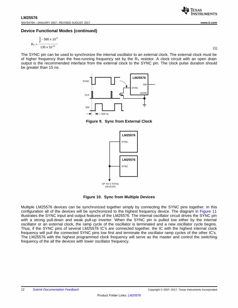
The SYNC pin can be used to synchronize the internal oscillator to an external clock. The external clock must beof higher frequency than the free-running frequency set by the RT resistor. A clock circuit with an open drainoutput is the recommended interface from the external clock to the SYNC pin. The clock pulse duration shouldbe greater than 15 ns.
Figure 9. Sync from External Clock
Figure 10. Sync from Multiple Devices
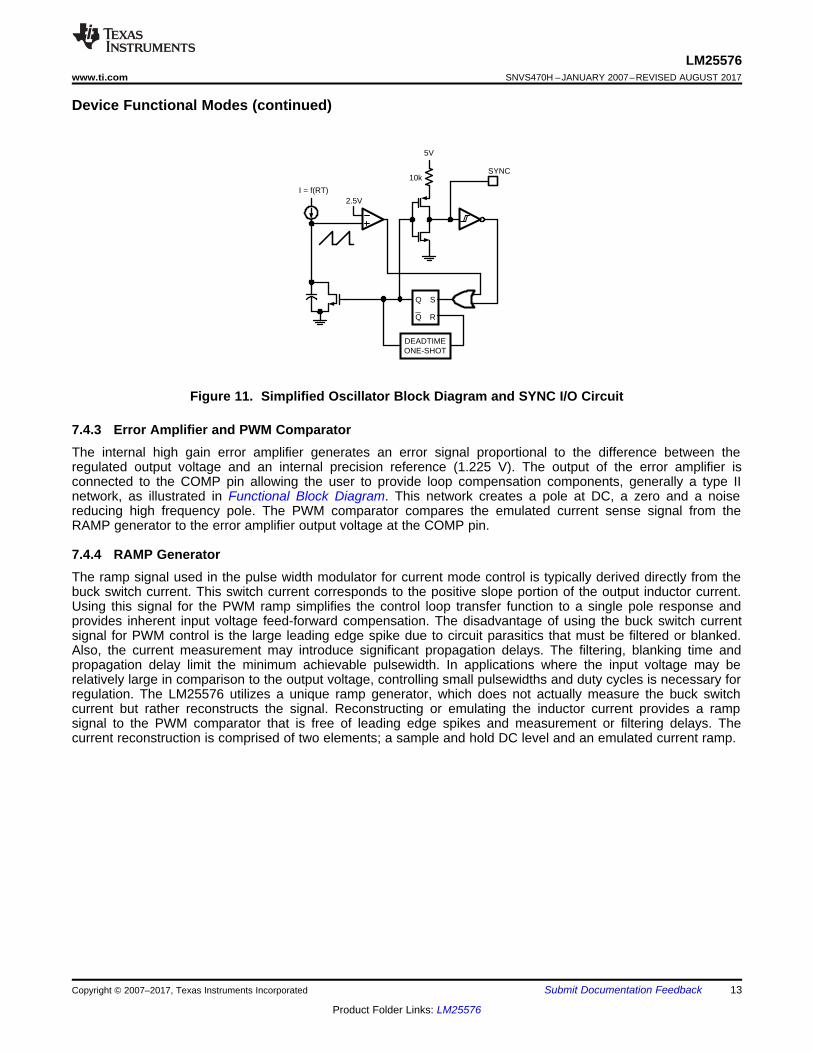
Multiple LM25576 devices can be synchronized together simply by connecting the SYNC pins together. In thisconfiguration all of the devices will be synchronized to the highest frequency device. The diagram in Figure 11illustrates the SYNC input and output features of the LM25576. The internal oscillator circuit drives the SYNC pinwith a strong pull-down and weak pull-up inverter. When the SYNC pin is pulled low either by the internaloscillator or an external clock, the ramp cycle of the oscillator is terminated and a new oscillator cycle begins.Thus, if the SYNC pins of several LM25576 IC’s are connected together, the IC with the highest internal clockfrequency will pull the connected SYNC pins low first and terminate the oscillator ramp cycles of the other IC’s.The LM25576 with the highest programmed clock frequency will serve as the master and control the switchingfrequency of the all the devices with lower oscillator frequency.
SYNC10k
S
R
Q
Q
DEADTIMEONE-SHOT
5V
2.5VI = f(RT)
13
LM25576www.ti.com SNVS470H –JANUARY 2007–REVISED AUGUST 2017
Product Folder Links: LM25576
Submit Documentation FeedbackCopyright © 2007–2017, Texas Instruments Incorporated
Device Functional Modes (continued)
Figure 11. Simplified Oscillator Block Diagram and SYNC I/O Circuit
7.4.3 Error Amplifier and PWM ComparatorThe internal high gain error amplifier generates an error signal proportional to the difference between theregulated output voltage and an internal precision reference (1.225 V). The output of the error amplifier isconnected to the COMP pin allowing the user to provide loop compensation components, generally a type IInetwork, as illustrated in Functional Block Diagram. This network creates a pole at DC, a zero and a noisereducing high frequency pole. The PWM comparator compares the emulated current sense signal from theRAMP generator to the error amplifier output voltage at the COMP pin.
7.4.4 RAMP GeneratorThe ramp signal used in the pulse width modulator for current mode control is typically derived directly from thebuck switch current. This switch current corresponds to the positive slope portion of the output inductor current.Using this signal for the PWM ramp simplifies the control loop transfer function to a single pole response andprovides inherent input voltage feed-forward compensation. The disadvantage of using the buck switch currentsignal for PWM control is the large leading edge spike due to circuit parasitics that must be filtered or blanked.Also, the current measurement may introduce significant propagation delays. The filtering, blanking time andpropagation delay limit the minimum achievable pulsewidth. In applications where the input voltage may berelatively large in comparison to the output voltage, controlling small pulsewidths and duty cycles is necessary forregulation. The LM25576 utilizes a unique ramp generator, which does not actually measure the buck switchcurrent but rather reconstructs the signal. Reconstructing or emulating the inductor current provides a rampsignal to the PWM comparator that is free of leading edge spikes and measurement or filtering delays. Thecurrent reconstruction is comprised of two elements; a sample and hold DC level and an emulated current ramp.

Sample andHold DC Level
0.5V/A
RAMP
TON
tON
CRAMP(5P x (VIN ± VOUT) + 25P) x
14
LM25576SNVS470H –JANUARY 2007–REVISED AUGUST 2017 www.ti.com
Product Folder Links: LM25576
Submit Documentation Feedback Copyright © 2007–2017, Texas Instruments Incorporated
Device Functional Modes (continued)
Figure 12. Composition of Current Sense Signal
The sample and hold DC level illustrated in Figure 12 is derived from a measurement of the re-circulatingSchottky diode anode current. The re-circulating diode anode should be connected to the IS pin. The diodecurrent flows through an internal current sense resistor between the IS and PGND pins. The voltage level acrossthe sense resistor is sampled and held just prior to the onset of the next conduction interval of the buck switch.The diode current sensing and sample & hold provide the DC level of the reconstructed current signal. Thepositive slope inductor current ramp is emulated by an external capacitor connected from the RAMP pin to AGNDand an internal voltage controlled current source. The ramp current source that emulates the inductor current is afunction of the Vin and Vout voltages per the following equation:
IRAMP = (5µ x (Vin – Vout)) + 25µA (2)
Proper selection of the RAMP capacitor depends upon the selected value of the output inductor. The value ofCRAMP can be selected from: CRAMP = L x 10-5, where L is the value of the output inductor in Henrys. With thisvalue, the scale factor of the emulated current ramp will be approximately equal to the scale factor of the DClevel sample and hold ( 0.5 V / A). The CRAMP capacitor should be located very close to the device andconnected directly to the pins of the IC (RAMP and AGND).
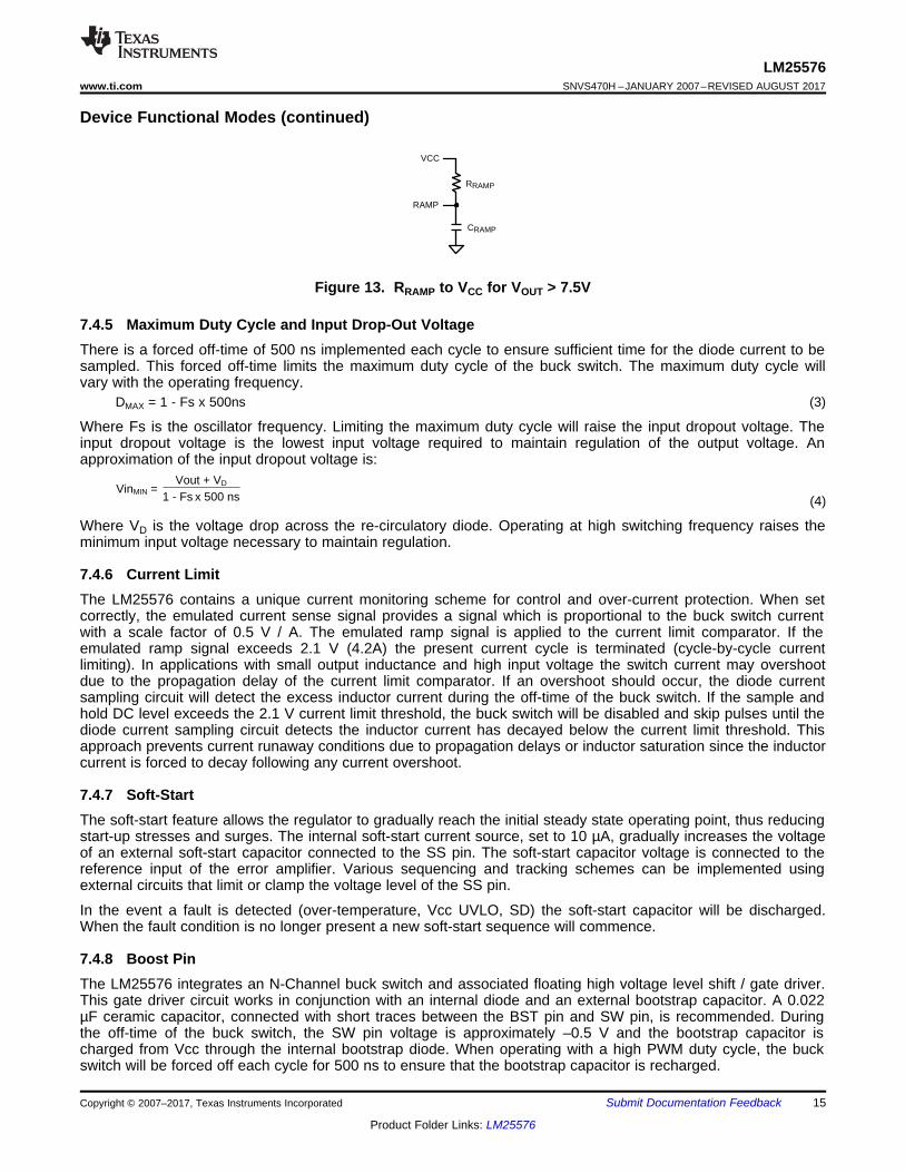
For duty cycles greater than 50%, peak current mode control circuits are subject to sub-harmonic oscillation.Sub-harmonic oscillation is normally characterized by observing alternating wide and narrow pulses at the switchnode. Adding a fixed slope voltage ramp (slope compensation) to the current sense signal prevents thisoscillation. The 25 µA of offset current provided from the emulated current source adds some fixed slope to theramp signal. In some high output voltage, high duty cycle applications, additional slope may be required. In theseapplications, a pull-up resistor may be added between the VCC and RAMP pins to increase the ramp slopecompensation.
For VOUT > 7.5V:
Calculate optimal slope current, IOS = VOUT x 5µA/V.
For example, at VOUT = 10V, IOS = 50µA.
Install a resistor from the RAMP pin to VCC:
RRAMP = VCC / (IOS - 25µA)
VinMIN =Vout + VD
1 - Fs x 500 ns
RAMP
VCC
CRAMP
RRAMP
15
LM25576www.ti.com SNVS470H –JANUARY 2007–REVISED AUGUST 2017
Product Folder Links: LM25576
Submit Documentation FeedbackCopyright © 2007–2017, Texas Instruments Incorporated
Device Functional Modes (continued)
Figure 13. RRAMP to VCC for VOUT > 7.5V
7.4.5 Maximum Duty Cycle and Input Drop-Out VoltageThere is a forced off-time of 500 ns implemented each cycle to ensure sufficient time for the diode current to besampled. This forced off-time limits the maximum duty cycle of the buck switch. The maximum duty cycle willvary with the operating frequency.
DMAX = 1 - Fs x 500ns (3)
Where Fs is the oscillator frequency. Limiting the maximum duty cycle will raise the input dropout voltage. Theinput dropout voltage is the lowest input voltage required to maintain regulation of the output voltage. Anapproximation of the input dropout voltage is:
(4)
Where VD is the voltage drop across the re-circulatory diode. Operating at high switching frequency raises theminimum input voltage necessary to maintain regulation.
7.4.6 Current LimitThe LM25576 contains a unique current monitoring scheme for control and over-current protection. When setcorrectly, the emulated current sense signal provides a signal which is proportional to the buck switch currentwith a scale factor of 0.5 V / A. The emulated ramp signal is applied to the current limit comparator. If theemulated ramp signal exceeds 2.1 V (4.2A) the present current cycle is terminated (cycle-by-cycle currentlimiting). In applications with small output inductance and high input voltage the switch current may overshootdue to the propagation delay of the current limit comparator. If an overshoot should occur, the diode currentsampling circuit will detect the excess inductor current during the off-time of the buck switch. If the sample andhold DC level exceeds the 2.1 V current limit threshold, the buck switch will be disabled and skip pulses until thediode current sampling circuit detects the inductor current has decayed below the current limit threshold. Thisapproach prevents current runaway conditions due to propagation delays or inductor saturation since the inductorcurrent is forced to decay following any current overshoot.
7.4.7 Soft-StartThe soft-start feature allows the regulator to gradually reach the initial steady state operating point, thus reducingstart-up stresses and surges. The internal soft-start current source, set to 10 µA, gradually increases the voltageof an external soft-start capacitor connected to the SS pin. The soft-start capacitor voltage is connected to thereference input of the error amplifier. Various sequencing and tracking schemes can be implemented usingexternal circuits that limit or clamp the voltage level of the SS pin.
In the event a fault is detected (over-temperature, Vcc UVLO, SD) the soft-start capacitor will be discharged.When the fault condition is no longer present a new soft-start sequence will commence.
7.4.8 Boost PinThe LM25576 integrates an N-Channel buck switch and associated floating high voltage level shift / gate driver.This gate driver circuit works in conjunction with an internal diode and an external bootstrap capacitor. A 0.022µF ceramic capacitor, connected with short traces between the BST pin and SW pin, is recommended. Duringthe off-time of the buck switch, the SW pin voltage is approximately –0.5 V and the bootstrap capacitor ischarged from Vcc through the internal bootstrap diode. When operating with a high PWM duty cycle, the buckswitch will be forced off each cycle for 500 ns to ensure that the bootstrap capacitor is recharged.

16
LM25576SNVS470H –JANUARY 2007–REVISED AUGUST 2017 www.ti.com
Product Folder Links: LM25576
Submit Documentation Feedback Copyright © 2007–2017, Texas Instruments Incorporated
Device Functional Modes (continued)Under very light load conditions or when the output voltage is pre-charged, the SW voltage will not remain lowduring the off-time of the buck switch. If the inductor current falls to zero and the SW pin rises, the bootstrapcapacitor will not receive sufficient voltage to operate the buck switch gate driver. For these applications, thePRE pin can be connected to the SW pin to pre-charge the bootstrap capacitor. The internal pre-chargeMOSFET and diode connected between the PRE pin and PGND turns on each cycle for 265 ns just prior to theonset of a new switching cycle. If the SW pin is at a normal negative voltage level (continuous conduction mode),then no current will flow through the pre-charge MOSFET/diode.
7.4.9 Thermal ProtectionInternal Thermal Shutdown circuitry is provided to protect the integrated circuit in the event the maximum junctiontemperature is exceeded. When activated, typically at 165°C, the controller is forced into a low power reset state,disabling the output driver and the bias regulator. This feature is provided to prevent catastrophic failures fromaccidental device overheating.

RT =[(1 / 300 x 103) ± 580 x 10-9]
135 x 10-12
17
LM25576www.ti.com SNVS470H –JANUARY 2007–REVISED AUGUST 2017
Product Folder Links: LM25576
Submit Documentation FeedbackCopyright © 2007–2017, Texas Instruments Incorporated
8 Application and Implementation
NOTEInformation in the following applications sections is not part of the TI componentspecification, and TI does not warrant its accuracy or completeness. TI’s customers areresponsible for determining suitability of components for their purposes. Customers shouldvalidate and test their design implementation to confirm system functionality.
8.1 Application Information
8.1.1 External ComponentsThe procedure for calculating the external components is illustrated with the following design example. The Bill ofMaterials for this design is listed in Table 1. The circuit shown in Functional Block Diagram is configured for thefollowing specifications:• VOUT = 5 V• VIN = 7 V to 42 V• Fs = 300 kHz• Minimum load current (for CCM) = 250 mA• Maximum load current = 3 A
8.1.2 R3 (RT)RT sets the oscillator switching frequency. Generally, higher frequency applications are smaller but have higherlosses. Operation at 300 kHz was selected for this example as a reasonable compromise for both small size andhigh efficiency. The value of RT for 300 kHz switching frequency can be calculated as follows:
(5)
The nearest standard value of 21 kΩ was chosen for RT.
'VOUT = 'IL x1
8 x FS x COUT
§¨©ESR + §
¨©
L1 =5V x (42V ± 5V)
0.5A x 300 kHz x 42V = 29 PH
L1 =VOUT x (VIN(max) ± VOUT)
IRIPPLE x FS x VIN(max)
IPK+
L1
Cu
rren
t
0 mA
IPK-
IOIRIPPLE
1/Fs
18
LM25576SNVS470H –JANUARY 2007–REVISED AUGUST 2017 www.ti.com
Product Folder Links: LM25576
Submit Documentation Feedback Copyright © 2007–2017, Texas Instruments Incorporated
Application Information (continued)8.1.3 L1The inductor value is determined based on the operating frequency, load current, ripple current, and theminimum and maximum input voltage (VIN(min), VIN(max)).
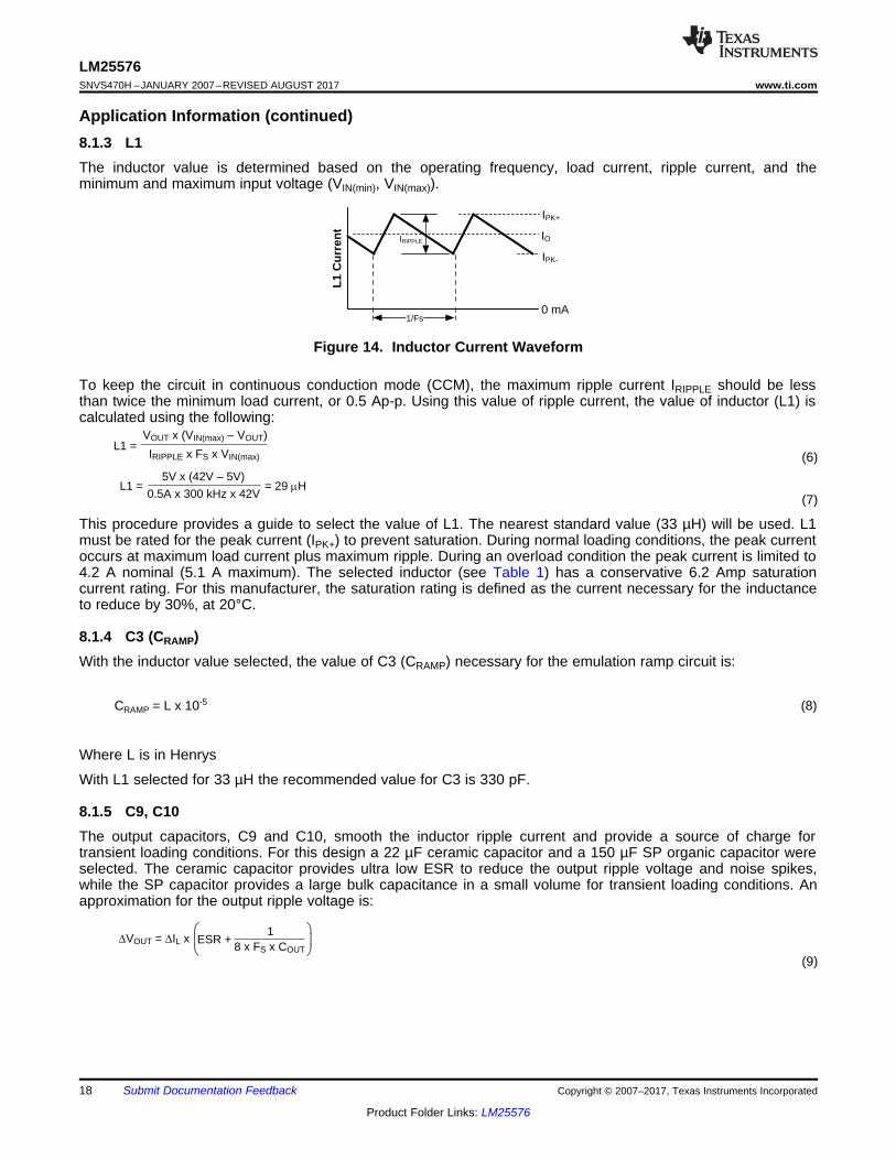
Figure 14. Inductor Current Waveform
To keep the circuit in continuous conduction mode (CCM), the maximum ripple current IRIPPLE should be lessthan twice the minimum load current, or 0.5 Ap-p. Using this value of ripple current, the value of inductor (L1) iscalculated using the following:
(6)
(7)
This procedure provides a guide to select the value of L1. The nearest standard value (33 µH) will be used. L1must be rated for the peak current (IPK+) to prevent saturation. During normal loading conditions, the peak currentoccurs at maximum load current plus maximum ripple. During an overload condition the peak current is limited to4.2 A nominal (5.1 A maximum). The selected inductor (see Table 1) has a conservative 6.2 Amp saturationcurrent rating. For this manufacturer, the saturation rating is defined as the current necessary for the inductanceto reduce by 30%, at 20°C.
8.1.4 C3 (CRAMP)With the inductor value selected, the value of C3 (CRAMP) necessary for the emulation ramp circuit is:
CRAMP = L x 10-5 (8)
Where L is in Henrys
With L1 selected for 33 µH the recommended value for C3 is 330 pF.
8.1.5 C9, C10The output capacitors, C9 and C10, smooth the inductor ripple current and provide a source of charge fortransient loading conditions. For this design a 22 µF ceramic capacitor and a 150 µF SP organic capacitor wereselected. The ceramic capacitor provides ultra low ESR to reduce the output ripple voltage and noise spikes,while the SP capacitor provides a large bulk capacitance in a small volume for transient loading conditions. Anapproximation for the output ripple voltage is:
(9)

tss =C4 x 1.225V
10 PA
19
LM25576www.ti.com SNVS470H –JANUARY 2007–REVISED AUGUST 2017
Product Folder Links: LM25576
Submit Documentation FeedbackCopyright © 2007–2017, Texas Instruments Incorporated
Application Information (continued)8.1.6 D1A Schottky type re-circulating diode is required for all LM25576 applications. Ultra-fast diodes are notrecommended and may result in damage to the IC due to reverse recovery current transients. The near idealreverse recovery characteristics and low forward voltage drop are particularly important diode characteristics forhigh input voltage and low output voltage applications common to the LM25576. The reverse recoverycharacteristic determines how long the current surge lasts each cycle when the buck switch is turned on. Thereverse recovery characteristics of Schottky diodes minimize the peak instantaneous power in the buck switchoccurring during turn-on each cycle. The resulting switching losses of the buck switch are significantly reducedwhen using a Schottky diode. The reverse breakdown rating should be selected for the maximum VIN, plus somesafety margin.
The forward voltage drop has a significant impact on the conversion efficiency, especially for applications with alow output voltage. “Rated” current for diodes vary widely from various manufacturers. The worst case is toassume a short circuit load condition. In this case the diode will carry the output current almost continuously. Forthe LM25576 this current can be as high as 4.2 A. Assuming a worst case 1 V drop across the diode, themaximum diode power dissipation can be as high as 4.2 W. For the reference design a 60 V Schottky in a DPAKpackage was selected.
8.1.7 C1, C2The regulator supply voltage has a large source impedance at the switching frequency. Good quality inputcapacitors are necessary to limit the ripple voltage at the VIN pin while supplying most of the switch currentduring the on-time. When the buck switch turns on, the current into the VIN pin steps to the lower peak of theinductor current waveform, ramps up to the peak value, then drops to zero at turn-off. The average current intoVIN during the on-time is the load current. The input capacitance should be selected for RMS current rating andminimum ripple voltage. A good approximation for the required ripple current rating necessary is IRMS > IOUT / 2.
Quality ceramic capacitors with a low ESR should be selected for the input filter. To allow for capacitortolerances and voltage effects, two 2.2 µF, 100 V ceramic capacitors will be used. If step input voltage transientsare expected near the maximum rating of the LM25576, a careful evaluation of ringing and possible spikes at thedevice VIN pin should be completed. An additional damping network or input voltage clamp may be required inthese cases.
8.1.8 C8The capacitor at the VCC pin provides noise filtering and stability for the VCC regulator. The recommended valueof C8 should be no smaller than 0.1 µF, and should be a good quality, low ESR, ceramic capacitor. A value of0.47 µF was selected for this design.
8.1.9 C7The bootstrap capacitor between the BST and the SW pins supplies the gate current to charge the buck switchgate at turn-on. The recommended value of C7 is 0.022 µF, and should be a good quality, low ESR, ceramiccapacitor.
8.1.10 C4The capacitor at the SS pin determines the soft-start time, that is the time for the reference voltage and theoutput voltage, to reach the final regulated value. The time is determined from:
(10)
For this application, a C4 value of 0.01 µF was chosen which corresponds to a soft-start time of 1 ms.
8.1.11 R5, R6R5 and R6 set the output voltage level, the ratio of these resistors is calculated from:
R5/R6 = (VOUT / 1.225V) - 1 (11)

R2 = 1.225 xR1
VIN(min) + (5 x 10⁻⁶ x R1) ± 1.225
§¨©
§¨©
20
LM25576SNVS470H –JANUARY 2007–REVISED AUGUST 2017 www.ti.com
Product Folder Links: LM25576
Submit Documentation Feedback Copyright © 2007–2017, Texas Instruments Incorporated
Application Information (continued)For a 5 V output, the R5 and R6 ratio calculates to 3.082. The resistors should be chosen from standard valueresistors, a good starting point is selection in the range of 1 kΩ - 10 kΩ. Values of 5.11 kΩ for R5, and 1.65 kΩfor R6 were selected.
8.1.12 R1, R2, C12A voltage divider can be connected to the SD pin to set a minimum operating voltage Vin(min) for the regulator. Ifthis feature is required, the easiest approach to select the divider resistor values is to select a value for R1(between 10 kΩ and 100 kΩ recommended) then calculate R2 from:
(12)
Capacitor C12 provides filtering for the divider. The voltage at the SD pin should never exceed 8 V, when usingan external set-point divider it may be necessary to clamp the SD pin at high input voltage conditions. Thereference design utilizes the full range of the LM25576 (6 V to 42 V); therefore these components can beomitted. With the SD pin open circuit the LM25576 responds once the Vcc UVLO threshold is satisfied.
8.1.13 R7, C11A snubber network across the power diode reduces ringing and spikes at the switching node. Excessive ringingand spikes can cause erratic operation and couple spikes and noise to the output. Voltage spikes beyond therating of the LM25576 or the re-circulating diode can damage these devices. Selecting the values for the snubberis best accomplished through empirical methods. First, make sure the lead lengths for the snubber connectionsare very short. For the current levels typical for the LM25576 a resistor value between 5 and 20 Ohms isadequate. Increasing the value of the snubber capacitor results in more damping but higher losses. Select aminimum value of C11 that provides adequate damping of the SW pin waveform at high load.
8.1.14 R4, C5, C6These components configure the error amplifier gain characteristics to accomplish a stable overall loop gain. Oneadvantage of current mode control is the ability to close the loop with only two feedback components, R4 and C5.The overall loop gain is the product of the modulator gain and the error amplifier gain. The DC modulator gain ofthe LM25576 is as follows:
DC Gain(MOD) = Gm(MOD) x RLOAD = 2 x RLOAD (13)
The dominant low frequency pole of the modulator is determined by the load resistance (RLOAD,) and outputcapacitance (COUT). The corner frequency of this pole is:
fp(MOD) = 1 / (2π RLOAD COUT) (14)
For RLOAD = 5Ω and COUT = 177µF then fp(MOD) = 180Hz
DC Gain(MOD) = 2 x 5 = 10 = 20dB
For the design example of Functional Block Diagram the following modulator gain vs. frequency characteristicwas measured as shown in Figure 15.

REF LEVEL0.000 dB0.0 deg
100 1k
START 50.000 Hz
10k
STOP 50 000.000 Hz
/DIV10.000 dB45.000 deg
0
GAIN
PHASE
REF LEVEL0.000 dB0.0 deg
100 1k
START 50.000 Hz
10k
STOP 50 000.000 Hz
/DIV10.000 dB45.000 deg
0
GAIN
PHASE
21
LM25576www.ti.com SNVS470H –JANUARY 2007–REVISED AUGUST 2017
Product Folder Links: LM25576
Submit Documentation FeedbackCopyright © 2007–2017, Texas Instruments Incorporated
Application Information (continued)
Figure 15. Gain and Phase of ModulatorRLOAD = 5 Ohms and COUT = 177µF
Components R4 and C5 configure the error amplifier as a type II configuration which has a pole at DC and azero at fZ = 1 / (2πR4C5). The error amplifier zero cancels the modulator pole leaving a single pole response atthe crossover frequency of the loop gain. A single pole response at the crossover frequency yields a very stableloop with 90 degrees of phase margin.
For the design example, a target loop bandwidth (crossover frequency) of 20 kHz was selected. Thecompensation network zero (fZ) should be selected at least an order of magnitude less than the target crossoverfrequency. This constrains the product of R4 and C5 for a desired compensation network zero 1 / (2π R4 C5) tobe less than 2 kHz. Increasing R4, while proportionally decreasing C5, increases the error amp gain. Conversely,decreasing R4 while proportionally increasing C5, decreases the error amp gain. For the design example C5 wasselected for 0.01 µF and R4 was selected for 49.9 kΩ. These values configure the compensation network zero at320 Hz. The error amp gain at frequencies greater than fZ is: R4 / R5, which is approximately 10 (20dB).
Figure 16. Error Amplifier Gain and Phase
The overall loop can be predicted as the sum (in dB) of the modulator gain and the error amp gain.
REF LEVEL0.000 dB0.0 deg
100 1k
START 50.000 Hz
10k
STOP 50 000.000 Hz
/DIV10.000 dB45.000 deg
0
GAIN
PHASE
22
LM25576SNVS470H –JANUARY 2007–REVISED AUGUST 2017 www.ti.com
Product Folder Links: LM25576
Submit Documentation Feedback Copyright © 2007–2017, Texas Instruments Incorporated
Application Information (continued)
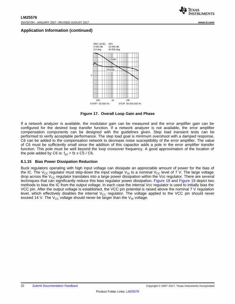
Figure 17. Overall Loop Gain and Phase
If a network analyzer is available, the modulator gain can be measured and the error amplifier gain can beconfigured for the desired loop transfer function. If a network analyzer is not available, the error amplifiercompensation components can be designed with the guidelines given. Step load transient tests can beperformed to verify acceptable performance. The step load goal is minimum overshoot with a damped response.C6 can be added to the compensation network to decrease noise susceptibility of the error amplifier. The valueof C6 must be sufficiently small since the addition of this capacitor adds a pole in the error amplifier transferfunction. This pole must be well beyond the loop crossover frequency. A good approximation of the location ofthe pole added by C6 is: fp2 = fz x C5 / C6.
8.1.15 Bias Power Dissipation ReductionBuck regulators operating with high input voltage can dissipate an appreciable amount of power for the bias ofthe IC. The VCC regulator must step-down the input voltage VIN to a nominal VCC level of 7 V. The large voltagedrop across the VCC regulator translates into a large power dissipation within the Vcc regulator. There are severaltechniques that can significantly reduce this bias regulator power dissipation. Figure 18 and Figure 19 depict twomethods to bias the IC from the output voltage. In each case the internal Vcc regulator is used to initially bias theVCC pin. After the output voltage is established, the VCC pin potential is raised above the nominal 7 V regulationlevel, which effectively disables the internal VCC regulator. The voltage applied to the VCC pin should neverexceed 14 V. The VCC voltage should never be larger than the VIN voltage.

BST
SW
VCC
IS
GND
LM25576
COUT
D1
L1
D2
VOUT
BST
SW
VCC
IS
GND
LM25576
VOUT
D2
D1
L1
COUT
23
LM25576www.ti.com SNVS470H –JANUARY 2007–REVISED AUGUST 2017
Product Folder Links: LM25576
Submit Documentation FeedbackCopyright © 2007–2017, Texas Instruments Incorporated
Application Information (continued)
Figure 18. VCC Bias from VOUT for 8 V < VOUT < 14 V
Figure 19. VCC Bias with Additional Winding on the Output Inductor

33P
LM25576
VIN SW
BST
IS
FBCOMPGNDSS VCCRAMP
10V - 30V
0.022
0.47330p
OUT
0.01
D1
0.1
0.022
49.9k
10k
1.4k
CSHD6-604.4
SD
RT
21k
1k
7.15k
170
-10V
5.11k
3.01k
BST
SW
COMP
FB
SSRAMP RT VCC
VIN
OUT
IS
GND
9V - 32V
3.3V, 3ASD
SYNC
0.01P
47p0.01P
CSHD6-40
3.57k
LM25576
0.1P
49.9k
3.3P
140P
4.7P0.022P
24
LM25576SNVS470H –JANUARY 2007–REVISED AUGUST 2017 www.ti.com
Product Folder Links: LM25576
Submit Documentation Feedback Copyright © 2007–2017, Texas Instruments Incorporated
8.2 Typical Application
8.2.1 Typical Schematic for High Frequency (1 MHz) Application
Figure 20. Schematic 3.3 V, 3 A, 1 MHz
8.2.2 Typical Schematic for Buck and Boost (Inverting) Application
8.2.3 Detailed Design Procedure
8.2.3.1 Custom Design With WEBENCH® ToolsClick here to create a custom design using the LM25576 device with the WEBENCH® Power Designer.1. Start by entering the input voltage ( VIN), output voltage (VOUT), and output current (IOUT) requirements.2. Optimize the design for key parameters such as efficiency, footprint, and cost using the optimizer dial.3. Compare the generated design with other possible solutions from Texas Instruments.
The WEBENCH Power Designer provides a customized schematic along with a list of materials with real-timepricing and component availability.
In most cases, these actions are available:• Run electrical simulations to see important waveforms and circuit performance• Run thermal simulations to understand board thermal performance• Export customized schematic and layout into popular CAD formats• Print PDF reports for the design, and share the design with colleagues
Get more information about WEBENCH tools at www.ti.com/WEBENCH.
25
LM25576www.ti.com SNVS470H –JANUARY 2007–REVISED AUGUST 2017
Product Folder Links: LM25576
Submit Documentation FeedbackCopyright © 2007–2017, Texas Instruments Incorporated
9 Layout
9.1 Layout Guidelines
9.1.1 PCB Layout and Thermal ConsiderationsThe circuit in Figure 19 serves as both a block diagram of the LM25576 and a typical application boardschematic for the LM25576. In a buck regulator there are two loops where currents are switched very fast. Thefirst loop starts from the input capacitors, to the regulator VIN pin, to the regulator SW pin, to the inductor thenout to the load. The second loop starts from the output capacitor ground, to the regulator PGND pins, to theregulator IS pins, to the diode anode, to the inductor and then out to the load. Minimizing the loop area of thesetwo loops reduces the stray inductance and minimizes noise and possible erratic operation. A ground plane inthe PC board is recommended as a means to connect the input filter capacitors to the output filter capacitors andthe PGND pins of the regulator. Connect all of the low power ground connections (CSS, RT, CRAMP) directly to theregulator AGND pin. Connect the AGND and PGND pins together through the topside copper area covering theentire underside of the device. Place several vias in this underside copper area to the ground plane.
The two highest power dissipating components are the re-circulating diode and the LM25576 regulator IC. Theeasiest method to determine the power dissipated within the LM25576 is to measure the total conversion losses(Pin – Pout) then subtract the power losses in the Schottky diode, output inductor and snubber resistor. Anapproximation for the Schottky diode loss is P = (1-D) x Iout x Vfwd. An approximation for the output inductorpower is P = IOUT
2 x R x 1.1, where R is the DC resistance of the inductor and the 1.1 factor is an approximationfor the AC losses. If a snubber is used, an approximation for the damping resistor power dissipation is P = Vin2 xFsw x Csnub, where Fsw is the switching frequency and Csnub is the snubber capacitor. The regulator has anexposed thermal pad to aid power dissipation. Adding several vias under the device to the ground plane willgreatly reduce the regulator junction temperature. Selecting a diode with an exposed pad will aid the powerdissipation of the diode.
The most significant variables that affect the power dissipated by the LM25576 are the output current, inputvoltage and operating frequency. The power dissipated while operating near the maximum output current andmaximum input volatge can be appreciable. The operating frequency of the LM25576 evaluation board has beendesigned for 300 kHz. When operating at 3 A output current with a 42 V input the power dissipation of theLM25576 regulator is approximately 1.9 W.
The junction-to-ambient thermal resistance of the LM25576 will vary with the application. The most significantvariables are the area of copper in the PC board, the number of vias under the IC exposed pad and the amountof forced air cooling provided. Referring to the evaluation board artwork, the area under the LM25576(component side) is covered with copper and there are 5 connection vias to the solder side ground plane.Additional vias under the IC will have diminishing value as more vias are added. The integrity of the solderconnection from the IC exposed pad to the PC board is critical. Excessive voids will greatly diminish the thermaldissipation capacity. The junction-to-ambient thermal resistance of the LM25576 mounted in the evaluation boardvaries from 45°C/W with no airflow to 25°C/W with 900 LFM (Linear Feet per Minute). With a 25°C ambienttemperature and no airflow, the predicted junction temperature for the LM25576 will be 25 + (45 x 1.9) = 110°C.If the evaluation board is operated at 3 A output current and 42 V input voltage for a prolonged period of time thethermal shutdown protection within the IC may activate. The IC will turn off allowing the junction to cool, followedby restart with the soft-start capacitor reset to zero.
Table 1. 5 V, 3 A Demo Board Bill of MaterialsITEM PART NUMBER DESCRIPTION VALUE
C 1 C4532X7R2A225M CAPACITOR, CER, TDK 2.2µ, 100VC 2 C4532X7R2A225M CAPACITOR, CER, TDK 2.2µ, 100VC 3 C0805C331G1GAC CAPACITOR, CER, KEMET 330p, 100VC 4 C2012X7R2A103K CAPACITOR, CER, TDK 0.01µ, 100VC 5 C2012X7R2A103K CAPACITOR, CER, TDK 0.01µ, 100VC 6 OPEN NOT USEDC 7 C2012X7R2A223K CAPACITOR, CER, TDK 0.022µ, 100VC 8 C2012X7R1C474M CAPACITOR, CER, TDK 0.47µ, 16VC 9 C3225X7R1C226M CAPACITOR, CER, TDK 22µ, 16V

26
LM25576SNVS470H –JANUARY 2007–REVISED AUGUST 2017 www.ti.com
Product Folder Links: LM25576
Submit Documentation Feedback Copyright © 2007–2017, Texas Instruments Incorporated
Layout Guidelines (continued)Table 1. 5 V, 3 A Demo Board Bill of Materials (continued)
ITEM PART NUMBER DESCRIPTION VALUEC 10 EEFHE0J151R CAPACITOR, SP, PANASONIC 150µ, 6.3VC 11 C0805C331G1GAC CAPACITOR, CER, KEMET 330p, 100VC 12 OPEN NOT USEDD 1 CSHD6-60C DIODE, 60V, CENTRAL
6CWQ10FN DIODE, 100V, IR (D1-ALT)L 1 DR127-330 INDUCTOR, COOPER 33µHR 1 OPEN NOT USEDR 2 OPEN NOT USEDR 3 CRCW08052102F RESISTOR 21kΩR 4 CRCW08054992F RESISTOR 49.9kΩR 5 CRCW08055111F RESISTOR 5.11kΩR 6 CRCW08051651F RESISTOR 1.65kΩR 7 CRCW2512100J RESISTOR 10, 1WU 1 LM25576 REGULATOR, TEXAS INSTRUMENTS
9.2 Layout Example
Figure 21. Component Side
Figure 22. Solder Side

27
LM25576www.ti.com SNVS470H –JANUARY 2007–REVISED AUGUST 2017
Product Folder Links: LM25576
Submit Documentation FeedbackCopyright © 2007–2017, Texas Instruments Incorporated
Layout Example (continued)
Figure 23. Silkscreen

28
LM25576SNVS470H –JANUARY 2007–REVISED AUGUST 2017 www.ti.com
Product Folder Links: LM25576
Submit Documentation Feedback Copyright © 2007–2017, Texas Instruments Incorporated
10 Device and Documentation Support
10.1 Device Support
10.1.1 Developmental Support
10.1.1.1 Custom Design With WEBENCH® ToolsClick here to create a custom design using the LM25575 device with the WEBENCH® Power Designer.1. Start by entering the input voltage (VIN), output voltage (VOUT), and output current (IOUT) requirements.2. Optimize the design for key parameters such as efficiency, footprint, and cost using the optimizer dial.3. Compare the generated design with other possible solutions from Texas Instruments.
The WEBENCH Power Designer provides a customized schematic along with a list of materials with real-timepricing and component availability.
In most cases, these actions are available:• Run electrical simulations to see important waveforms and circuit performance• Run thermal simulations to understand board thermal performance• Export customized schematic and layout into popular CAD formats• Print PDF reports for the design, and share the design with colleagues
Get more information about WEBENCH tools at www.ti.com/WEBENCH.
10.2 Receiving Notification of Documentation UpdatesTo receive notification of documentation updates, navigate to the device product folder on ti.com. In the upperright corner, click on Alert me to register and receive a weekly digest of any product information that haschanged. For change details, review the revision history included in any revised document.
10.3 Community ResourcesThe following links connect to TI community resources. Linked contents are provided "AS IS" by the respectivecontributors. They do not constitute TI specifications and do not necessarily reflect TI's views; see TI's Terms ofUse.
TI E2E™ Online Community TI's Engineer-to-Engineer (E2E) Community. Created to foster collaborationamong engineers. At e2e.ti.com, you can ask questions, share knowledge, explore ideas and helpsolve problems with fellow engineers.
Design Support TI's Design Support Quickly find helpful E2E forums along with design support tools andcontact information for technical support.
10.4 TrademarksE2E is a trademark of Texas Instruments.WEBENCH is a registered trademark of Texas Instruments.All other trademarks are the property of their respective owners.
10.5 Electrostatic Discharge CautionThis integrated circuit can be damaged by ESD. Texas Instruments recommends that all integrated circuits be handled withappropriate precautions. Failure to observe proper handling and installation procedures can cause damage.
ESD damage can range from subtle performance degradation to complete device failure. Precision integrated circuits may be moresusceptible to damage because very small parametric changes could cause the device not to meet its published specifications.
10.6 GlossarySLYZ022 — TI Glossary.
This glossary lists and explains terms, acronyms, and definitions.
29
LM25576www.ti.com SNVS470H –JANUARY 2007–REVISED AUGUST 2017
Product Folder Links: LM25576
Submit Documentation FeedbackCopyright © 2007–2017, Texas Instruments Incorporated
11 Mechanical, Packaging, and Orderable InformationThe following pages include mechanical, packaging, and orderable information. This information is the mostcurrent data available for the designated devices. This data is subject to change without notice and revision ofthis document. For browser-based versions of this data sheet, refer to the left-hand navigation.
PACKAGE OPTION ADDENDUM
www.ti.com 18-Aug-2017
Addendum-Page 1
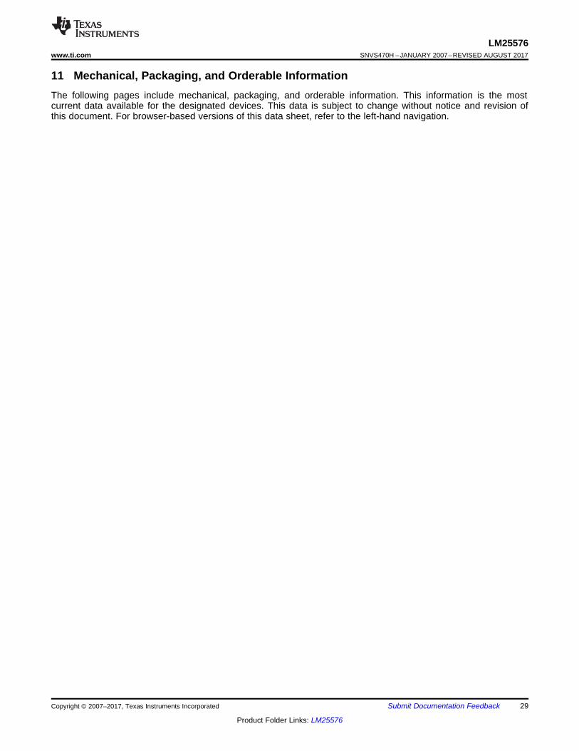
PACKAGING INFORMATION
Orderable Device Status(1)
Package Type PackageDrawing
Pins PackageQty
Eco Plan(2)
Lead/Ball Finish(6)
MSL Peak Temp(3)
Op Temp (°C) Device Marking(4/5)
Samples
LM25576MH/NOPB ACTIVE HTSSOP PWP 20 73 Green (RoHS& no Sb/Br)
CU SN Level-1-260C-UNLIM -40 to 125 LM25576MH
LM25576MHX NRND HTSSOP PWP 20 2500 TBD Call TI Call TI -40 to 125 LM25576MH
LM25576MHX/NOPB ACTIVE HTSSOP PWP 20 2500 Green (RoHS& no Sb/Br)
CU SN Level-1-260C-UNLIM -40 to 125 LM25576MH
(1) The marketing status values are defined as follows:ACTIVE: Product device recommended for new designs.LIFEBUY: TI has announced that the device will be discontinued, and a lifetime-buy period is in effect.NRND: Not recommended for new designs. Device is in production to support existing customers, but TI does not recommend using this part in a new design.PREVIEW: Device has been announced but is not in production. Samples may or may not be available.OBSOLETE: TI has discontinued the production of the device.
(2) RoHS: TI defines "RoHS" to mean semiconductor products that are compliant with the current EU RoHS requirements for all 10 RoHS substances, including the requirement that RoHS substancedo not exceed 0.1% by weight in homogeneous materials. Where designed to be soldered at high temperatures, "RoHS" products are suitable for use in specified lead-free processes. TI mayreference these types of products as "Pb-Free".RoHS Exempt: TI defines "RoHS Exempt" to mean products that contain lead but are compliant with EU RoHS pursuant to a specific EU RoHS exemption.Green: TI defines "Green" to mean the content of Chlorine (Cl) and Bromine (Br) based flame retardants meet JS709B low halogen requirements of <=1000ppm threshold. Antimony trioxide basedflame retardants must also meet the <=1000ppm threshold requirement.
(3) MSL, Peak Temp. - The Moisture Sensitivity Level rating according to the JEDEC industry standard classifications, and peak solder temperature.
(4) There may be additional marking, which relates to the logo, the lot trace code information, or the environmental category on the device.
(5) Multiple Device Markings will be inside parentheses. Only one Device Marking contained in parentheses and separated by a "~" will appear on a device. If a line is indented then it is a continuationof the previous line and the two combined represent the entire Device Marking for that device.
(6) Lead/Ball Finish - Orderable Devices may have multiple material finish options. Finish options are separated by a vertical ruled line. Lead/Ball Finish values may wrap to two lines if the finishvalue exceeds the maximum column width.
Important Information and Disclaimer:The information provided on this page represents TI's knowledge and belief as of the date that it is provided. TI bases its knowledge and belief on informationprovided by third parties, and makes no representation or warranty as to the accuracy of such information. Efforts are underway to better integrate information from third parties. TI has taken andcontinues to take reasonable steps to provide representative and accurate information but may not have conducted destructive testing or chemical analysis on incoming materials and chemicals.TI and TI suppliers consider certain information to be proprietary, and thus CAS numbers and other limited information may not be available for release.

PACKAGE OPTION ADDENDUM
www.ti.com 18-Aug-2017
Addendum-Page 2
In no event shall TI's liability arising out of such information exceed the total purchase price of the TI part(s) at issue in this document sold by TI to Customer on an annual basis.
OTHER QUALIFIED VERSIONS OF LM25576 :
• Automotive: LM25576-Q1
NOTE: Qualified Version Definitions:
• Automotive - Q100 devices qualified for high-reliability automotive applications targeting zero defects

TAPE AND REEL INFORMATION
*All dimensions are nominal
Device PackageType
PackageDrawing
Pins SPQ ReelDiameter
(mm)
ReelWidth
W1 (mm)
A0(mm)
B0(mm)
K0(mm)
P1(mm)
W(mm)
Pin1Quadrant
LM25576MHX HTSSOP PWP 20 2500 330.0 16.4 6.95 7.1 1.6 8.0 16.0 Q1
LM25576MHX/NOPB HTSSOP PWP 20 2500 330.0 16.4 6.95 7.1 1.6 8.0 16.0 Q1
PACKAGE MATERIALS INFORMATION
www.ti.com 3-Aug-2017
Pack Materials-Page 1
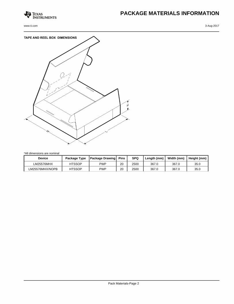
*All dimensions are nominal
Device Package Type Package Drawing Pins SPQ Length (mm) Width (mm) Height (mm)
LM25576MHX HTSSOP PWP 20 2500 367.0 367.0 35.0
LM25576MHX/NOPB HTSSOP PWP 20 2500 367.0 367.0 35.0
PACKAGE MATERIALS INFORMATION
www.ti.com 3-Aug-2017
Pack Materials-Page 2

MECHANICAL DATA
PWP0020A
www.ti.com
MXA20A (Rev C)

IMPORTANT NOTICE
Texas Instruments Incorporated (TI) reserves the right to make corrections, enhancements, improvements and other changes to itssemiconductor products and services per JESD46, latest issue, and to discontinue any product or service per JESD48, latest issue. Buyersshould obtain the latest relevant information before placing orders and should verify that such information is current and complete.TI’s published terms of sale for semiconductor products (http://www.ti.com/sc/docs/stdterms.htm) apply to the sale of packaged integratedcircuit products that TI has qualified and released to market. Additional terms may apply to the use or sale of other types of TI products andservices.Reproduction of significant portions of TI information in TI data sheets is permissible only if reproduction is without alteration and isaccompanied by all associated warranties, conditions, limitations, and notices. TI is not responsible or liable for such reproduceddocumentation. Information of third parties may be subject to additional restrictions. Resale of TI products or services with statementsdifferent from or beyond the parameters stated by TI for that product or service voids all express and any implied warranties for theassociated TI product or service and is an unfair and deceptive business practice. TI is not responsible or liable for any such statements.Buyers and others who are developing systems that incorporate TI products (collectively, “Designers”) understand and agree that Designersremain responsible for using their independent analysis, evaluation and judgment in designing their applications and that Designers havefull and exclusive responsibility to assure the safety of Designers' applications and compliance of their applications (and of all TI productsused in or for Designers’ applications) with all applicable regulations, laws and other applicable requirements. Designer represents that, withrespect to their applications, Designer has all the necessary expertise to create and implement safeguards that (1) anticipate dangerousconsequences of failures, (2) monitor failures and their consequences, and (3) lessen the likelihood of failures that might cause harm andtake appropriate actions. Designer agrees that prior to using or distributing any applications that include TI products, Designer willthoroughly test such applications and the functionality of such TI products as used in such applications.TI’s provision of technical, application or other design advice, quality characterization, reliability data or other services or information,including, but not limited to, reference designs and materials relating to evaluation modules, (collectively, “TI Resources”) are intended toassist designers who are developing applications that incorporate TI products; by downloading, accessing or using TI Resources in anyway, Designer (individually or, if Designer is acting on behalf of a company, Designer’s company) agrees to use any particular TI Resourcesolely for this purpose and subject to the terms of this Notice.TI’s provision of TI Resources does not expand or otherwise alter TI’s applicable published warranties or warranty disclaimers for TIproducts, and no additional obligations or liabilities arise from TI providing such TI Resources. TI reserves the right to make corrections,enhancements, improvements and other changes to its TI Resources. TI has not conducted any testing other than that specificallydescribed in the published documentation for a particular TI Resource.Designer is authorized to use, copy and modify any individual TI Resource only in connection with the development of applications thatinclude the TI product(s) identified in such TI Resource. NO OTHER LICENSE, EXPRESS OR IMPLIED, BY ESTOPPEL OR OTHERWISETO ANY OTHER TI INTELLECTUAL PROPERTY RIGHT, AND NO LICENSE TO ANY TECHNOLOGY OR INTELLECTUAL PROPERTYRIGHT OF TI OR ANY THIRD PARTY IS GRANTED HEREIN, including but not limited to any patent right, copyright, mask work right, orother intellectual property right relating to any combination, machine, or process in which TI products or services are used. Informationregarding or referencing third-party products or services does not constitute a license to use such products or services, or a warranty orendorsement thereof. Use of TI Resources may require a license from a third party under the patents or other intellectual property of thethird party, or a license from TI under the patents or other intellectual property of TI.TI RESOURCES ARE PROVIDED “AS IS” AND WITH ALL FAULTS. TI DISCLAIMS ALL OTHER WARRANTIES ORREPRESENTATIONS, EXPRESS OR IMPLIED, REGARDING RESOURCES OR USE THEREOF, INCLUDING BUT NOT LIMITED TOACCURACY OR COMPLETENESS, TITLE, ANY EPIDEMIC FAILURE WARRANTY AND ANY IMPLIED WARRANTIES OFMERCHANTABILITY, FITNESS FOR A PARTICULAR PURPOSE, AND NON-INFRINGEMENT OF ANY THIRD PARTY INTELLECTUALPROPERTY RIGHTS. TI SHALL NOT BE LIABLE FOR AND SHALL NOT DEFEND OR INDEMNIFY DESIGNER AGAINST ANY CLAIM,INCLUDING BUT NOT LIMITED TO ANY INFRINGEMENT CLAIM THAT RELATES TO OR IS BASED ON ANY COMBINATION OFPRODUCTS EVEN IF DESCRIBED IN TI RESOURCES OR OTHERWISE. IN NO EVENT SHALL TI BE LIABLE FOR ANY ACTUAL,DIRECT, SPECIAL, COLLATERAL, INDIRECT, PUNITIVE, INCIDENTAL, CONSEQUENTIAL OR EXEMPLARY DAMAGES INCONNECTION WITH OR ARISING OUT OF TI RESOURCES OR USE THEREOF, AND REGARDLESS OF WHETHER TI HAS BEENADVISED OF THE POSSIBILITY OF SUCH DAMAGES.Unless TI has explicitly designated an individual product as meeting the requirements of a particular industry standard (e.g., ISO/TS 16949and ISO 26262), TI is not responsible for any failure to meet such industry standard requirements.Where TI specifically promotes products as facilitating functional safety or as compliant with industry functional safety standards, suchproducts are intended to help enable customers to design and create their own applications that meet applicable functional safety standardsand requirements. Using products in an application does not by itself establish any safety features in the application. Designers mustensure compliance with safety-related requirements and standards applicable to their applications. Designer may not use any TI products inlife-critical medical equipment unless authorized officers of the parties have executed a special contract specifically governing such use.Life-critical medical equipment is medical equipment where failure of such equipment would cause serious bodily injury or death (e.g., lifesupport, pacemakers, defibrillators, heart pumps, neurostimulators, and implantables). Such equipment includes, without limitation, allmedical devices identified by the U.S. Food and Drug Administration as Class III devices and equivalent classifications outside the U.S.TI may expressly designate certain products as completing a particular qualification (e.g., Q100, Military Grade, or Enhanced Product).Designers agree that it has the necessary expertise to select the product with the appropriate qualification designation for their applicationsand that proper product selection is at Designers’ own risk. Designers are solely responsible for compliance with all legal and regulatoryrequirements in connection with such selection.Designer will fully indemnify TI and its representatives against any damages, costs, losses, and/or liabilities arising out of Designer’s non-compliance with the terms and provisions of this Notice.
Mailing Address: Texas Instruments, Post Office Box 655303, Dallas, Texas 75265Copyright © 2017, Texas Instruments Incorporated


