
LM2423 220V Monolithic Triple Channel 15 MHz CRT … Sheets/National...LM2423 220V Monolithic Triple...
11
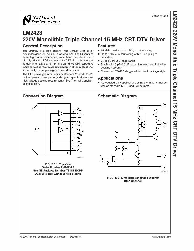
LM2423 220V Monolithic Triple Channel 15 MHz CRT DTV Driver General Description The LM2423 is a triple channel high voltage CRT driver circuit designed for use in DTV applications. The IC contains three high input impedance, wide band amplifiers which directly drive the RGB cathodes of a CRT. Each channel has its gain internally set to -54 and can drive CRT capacitive loads as well as resistive loads present in other applications, limited only by the package’s power dissipation. The IC is packaged in an industry standard 11-lead TO-220 molded plastic power package designed specifically to meet high voltage spacing requirements. See Thermal Consider- ations section. Features n 15 MHz bandwidth at 130V PP output swing n Up to 170V PP output swing with AC coupling to cathodes n 0V to 5V input voltage range n Stable with 0 pF–20 pF capacitive loads and inductive peaking networks n Convenient TO-220 staggered thin lead package style Applications n AC coupled DTV applications using the 480p format as well as standard NTSC and PAL formats. Connection Diagram Schematic Diagram 20114801 FIGURE 1. Top View Order Number LM2423TE See NS Package Number TE11B NOPB Available only with lead free plating 20114802 FIGURE 2. Simplified Schematic Diagram (One Channel) January 2006 LM2423 220V Monolithic Triple Channel 15 MHz CRT DTV Driver © 2006 National Semiconductor Corporation DS201148 www.national.com
-
Upload
duongthien -
Category
Documents
-
view
220 -
download
0
Transcript of LM2423 220V Monolithic Triple Channel 15 MHz CRT … Sheets/National...LM2423 220V Monolithic Triple...
LM2423220V Monolithic Triple Channel 15 MHz CRT DTV DriverGeneral DescriptionThe LM2423 is a triple channel high voltage CRT drivercircuit designed for use in DTV applications. The IC containsthree high input impedance, wide band amplifiers whichdirectly drive the RGB cathodes of a CRT. Each channel hasits gain internally set to −54 and can drive CRT capacitiveloads as well as resistive loads present in other applications,limited only by the package’s power dissipation.
The IC is packaged in an industry standard 11-lead TO-220molded plastic power package designed specifically to meethigh voltage spacing requirements. See Thermal Consider-ations section.
Featuresn 15 MHz bandwidth at 130VPP output swingn Up to 170VPP output swing with AC coupling to
cathodesn 0V to 5V input voltage rangen Stable with 0 pF–20 pF capacitive loads and inductive
peaking networksn Convenient TO-220 staggered thin lead package style
Applicationsn AC coupled DTV applications using the 480p format as
well as standard NTSC and PAL formats.
Connection Diagram Schematic Diagram
20114801
FIGURE 1. Top ViewOrder Number LM2423TE
See NS Package Number TE11B NOPBAvailable only with lead free plating
20114802
FIGURE 2. Simplified Schematic Diagram(One Channel)
January 2006LM
2423220V
Monolithic
TripleC
hannel15M
Hz
CR
TD
TVD
river
© 2006 National Semiconductor Corporation DS201148 www.national.com
Absolute Maximum Ratings (Notes 1,
3)
If Military/Aerospace specified devices are required,please contact the National Semiconductor Sales Office/Distributors for availability and specifications.
Supply Voltage (VCC) +250V
Bias Voltage (VBB) +16V
Input Voltage (VIN) −0.5V to VBB +0.5V
Storage Temperature Range (TSTG) −65˚C to +150˚C
Lead Temperature
(Soldering, <10 sec.) 300˚C
ESD Tolerance,
Machine Model 200V
Junction Temperature 150˚C
θJC (typ) 2.2˚C/W
Operating Ratings (Note 2)
VCC +100V to +230V
VBB +7V to +13V
VIN +0V to +5V
VOUT +40V to +215V
Case Temperature 110˚C
Do not operate the part without a heat sink.
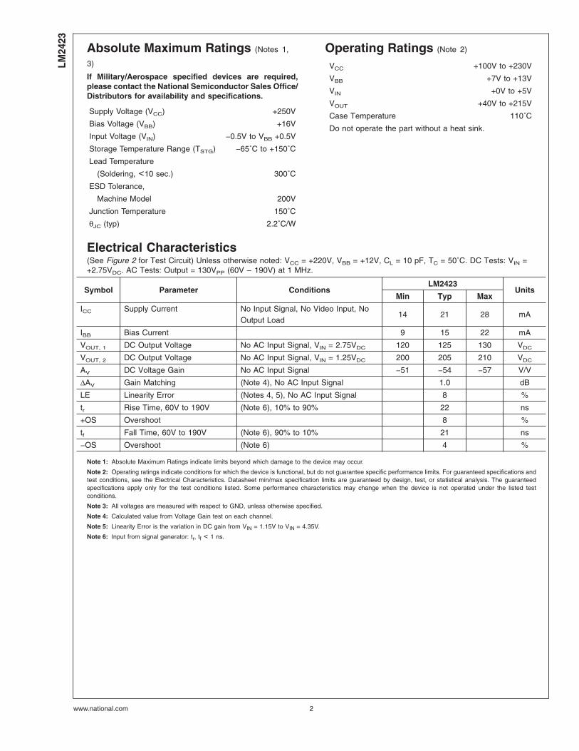
Electrical Characteristics(See Figure 2 for Test Circuit) Unless otherwise noted: VCC = +220V, VBB = +12V, CL = 10 pF, TC = 50˚C. DC Tests: VIN =+2.75VDC. AC Tests: Output = 130VPP (60V – 190V) at 1 MHz.
Symbol Parameter ConditionsLM2423
UnitsMin Typ Max
ICC Supply Current No Input Signal, No Video Input, NoOutput Load
14 21 28 mA
IBB Bias Current 9 15 22 mA
VOUT, 1 DC Output Voltage No AC Input Signal, VIN = 2.75VDC 120 125 130 VDC
VOUT, 2 DC Output Voltage No AC Input Signal, VIN = 1.25VDC 200 205 210 VDC
AV DC Voltage Gain No AC Input Signal −51 −54 −57 V/V
∆AV Gain Matching (Note 4), No AC Input Signal 1.0 dB
LE Linearity Error (Notes 4, 5), No AC Input Signal 8 %
tr Rise Time, 60V to 190V (Note 6), 10% to 90% 22 ns
+OS Overshoot 8 %
tf Fall Time, 60V to 190V (Note 6), 90% to 10% 21 ns
−OS Overshoot (Note 6) 4 %
Note 1: Absolute Maximum Ratings indicate limits beyond which damage to the device may occur.
Note 2: Operating ratings indicate conditions for which the device is functional, but do not guarantee specific performance limits. For guaranteed specifications andtest conditions, see the Electrical Characteristics. Datasheet min/max specification limits are guaranteed by design, test, or statistical analysis. The guaranteedspecifications apply only for the test conditions listed. Some performance characteristics may change when the device is not operated under the listed testconditions.
Note 3: All voltages are measured with respect to GND, unless otherwise specified.
Note 4: Calculated value from Voltage Gain test on each channel.
Note 5: Linearity Error is the variation in DC gain from VIN = 1.15V to VIN = 4.35V.
Note 6: Input from signal generator: tr, tf < 1 ns.
LM24
23
www.national.com 2

AC Test Circuit
Figure 3 shows a typical test circuit for evaluation of the LM2423. This circuit is designed to allow testing of the LM2423 in a 50Ωenvironment without the use of an expensive FET probe. The two 4990Ω resistors form a 400:1 divider with the 50Ω resistor andthe oscilloscope. A test point is included for easy use of an oscilloscope probe. The compensation capacitor is used tocompensate the network to achieve flat frequency response.
20114803
Note: 10 pF load includes parasitic capacitance.
FIGURE 3. Test Circuit (One Channel)
LM2423
www.national.com3
Typical Performance Characteristics 50˚C (VCC = +220VDC, VBB = +12VDC, CL = 10 pF, VOUT =130VPP (60V – 190V), TC = 50˚C, Test Circuit — Figure 3 unless otherwise specified)
20114804
FIGURE 4. VOUT vs VIN
20114805
FIGURE 5. LM2423 Pulse Response
20114806
FIGURE 6. Bandwidth
20114807
FIGURE 7. Speed vs Load Capacitance
20114808
FIGURE 8. Speed vs Offset
20114809
FIGURE 9. Speed vs Case Temperature
LM24
23
www.national.com 4
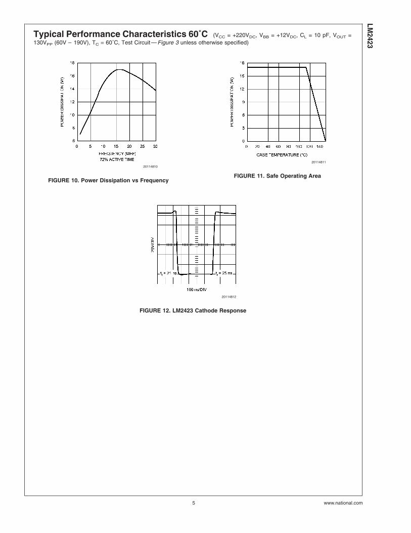
Typical Performance Characteristics 60˚C (VCC = +220VDC, VBB = +12VDC, CL = 10 pF, VOUT =130VPP (60V – 190V), TC = 60˚C, Test Circuit — Figure 3 unless otherwise specified)
20114810
FIGURE 10. Power Dissipation vs Frequency
20114811
FIGURE 11. Safe Operating Area
20114812
FIGURE 12. LM2423 Cathode Response
LM2423
www.national.com5

Theory of OperationThe LM2423 is a high voltage monolithic three channel CRTdriver suitable for DTV applications. The LM2423 operateswith 220V and 12V power supplies. The part is housed in theindustry standard 11-lead TO-220 molded plastic powerpackage with thin leads for improved metal-to-metal spacing.
The circuit diagram of the LM2423 is shown in Figure 2. ThePNP emitter follower, Q5, provides input buffering. Q1 andQ2 form a fixed gain cascode amplifier with resistors R1 andR2 setting the gain at −54. Emitter followers Q3 and Q4isolate the high output impedance of the cascode stage fromthe capacitance of the CRT cathode, which decreases thesensitivity of the device to load capacitance. Q6 providesbiasing to the output emitter follower stage to reduce cross-over distortion at low signal levels.
Figure 3 shows a typical test circuit for evaluation of theLM2423. This circuit is designed to allow testing of theLM2423 in a 50Ω environment without the use of an expen-sive FET probe. In this test circuit, the two 4.99 kΩ resistorsform a 400:1 wideband, low capacitance probe when con-nected to a 50Ω coaxial cable and a 50Ω load (such as a50Ω oscilloscope input). The input signal from the generatoris ac coupled to the base of Q5.
Application Hints
INTRODUCTION
National Semiconductor (NSC) is committed to provide ap-plication information that assists our customers in obtainingthe best performance possible from our products. The fol-lowing information is provided in order to support this com-mitment. The reader should be aware that the optimization ofperformance was done using a specific printed circuit boarddesigned at NSC. Variations in performance can be realizeddue to physical changes in the printed circuit board and theapplication. Therefore, the designer should know that com-ponent value changes may be required in order to optimizeperformance in a given application. The values shown in thisdocument can be used as a starting point for evaluationpurposes. When working with high bandwidth circuits, goodlayout practices are also critical to achieving maximum per-formance.
IMPORTANT INFORMATION
The LM2423 performance is targeted for the HDTV market.The application circuits shown in this document to optimizeperformance and to protect against damage from CRT arcover are designed specifically for the LM2423. If anothermember of the LM242X family is used, please refer to itsdatasheet.
POWER SUPPLY BYPASS
Since the LM2423 is a wide bandwidth amplifier, properpower supply bypassing is critical for optimum performance.Improper power supply bypassing can result in large over-shoot, ringing or oscillation. 0.1 µF capacitors should beconnected from the supply pins, VCC and VBB, to ground, asclose to the LM2423 as is practical. Additionally, a 22 µF orlarger electrolytic capacitor should be connected from bothsupply pins to ground reasonably close to the LM2423.
ARC PROTECTION
During normal CRT operation, internal arcing may occasion-ally occur. This fast, high voltage, high-energy pulse candamage the LM2423 output stage. The application circuit
shown in Figure 13 is designed to help clamp the voltage atthe output of the LM2423 to a safe level. The clamp diodes,D1 and D2, should have a fast transient response, high peakcurrent rating, low series impedance and low shunt capaci-tance. 1SS83 or equivalent diodes are recommended. D1and D2 should have short, low impedance connections toVCC and ground respectively. The cathode of D1 should belocated very close to a separately decoupled bypass capaci-tor (C3 in Figure 13). The ground connection of D2 and thedecoupling capacitor should be very close to the LM2423ground. This will significantly reduce the high frequencyvoltage transients that the LM2423 would be subjected toduring an arc over condition. Resistor R2 limits the arc overcurrent that is seen by the diodes while R1 limits the currentinto the LM2423 as well as the voltage stress at the outputsof the device. R2 should be a 1⁄2W solid carbon type resistor.R1 can be a 1⁄4W metal or carbon film type resistor. Havinglarge value resistors for R1 and R2 would be desirable, butthis has the effect of increasing rise and fall times. InductorL1 is critical to reduce the initial high frequency voltagelevels that the LM2423 would be subjected to. The inductorwill not only help protect the device but it will also helpminimize rise and fall times as well as minimize EMI. Forproper arc protection, it is important to not omit any of the arcprotection components shown in Figure 13.
EFFECT OF LOAD CAPACITANCE
Figure 7 shows the effect of increased load capacitance onthe speed of the device. This demonstrates the importanceof knowing the load capacitance in the application. Increas-ing the load capacitance from 10 pF to 20 pF adds about7 ns to both the rise and fall times. It is important to keep theboard capacitance as low as possible to maximize the speedof the driver.
EFFECT OF OFFSET
Figure 8 shows the variation in rise and fall times when theoutput offset of the device is varied from 120V to 130VDC.The rise and fall times both show a variation of about 6%relative to the center data point (125VDC). The rise timeincreases in speed with the increase in offset voltage and thefall time decreased in speed with the increase in offsetvoltage.
THERMAL CONSIDERATIONS
Figure 9 shows the performance of the LM2423 in the testcircuit shown in Figure 3 as a function of case temperature.The figure shows that both the rise and fall times of theLM2423 increase by approximately 14% as the case tem-perature increases from 30˚C to 110˚C. This corresponds toa speed degradation of 1.4% for every 10˚C rise in casetemperature.
20114813
FIGURE 13. One Channel of the LM2423 with theRecommended Application Circuit
LM24
23
www.national.com 6
Application Hints (Continued)
Figure 10 shows the maximum power dissipation of theLM2423 vs. Frequency when all three channels of the deviceare driving into a 10 pF load with a 130VP-P alternating onepixel on, one pixel off. The graph assumes a 72% active time(device operating at the specified frequency), which is typicalin a TV application. The other 28% of the time the device isassumed to be sitting at the black level (190V in this case).This graph gives the designer the information needed todetermine the heat sink requirement for his application. Thedesigner should note that if the load capacitance is in-creased the AC component of the total power dissipationwould also increase.
The LM2423 case temperature must be maintained below110˚C. If the maximum expected ambient temperature is60˚C and the maximum power dissipation is 17W (fromFigure 10, 15 MHz) then a maximum heat sink thermalresistance can be calculated:
This example assumes a capacitive load of 10 pF and noresistive load. The designer should note that if the loadcapacitance is increased the AC component of the totalpower dissipation will also increase.
OPTIMIZING TRANSIENT RESPONSE
Referring to Figure 13, there are three components (R1, R2and L1) that can be adjusted to optimize the transient re-sponse of the application circuit. Increasing the values of R1and R2 will slow the circuit down while decreasing over-shoot. Increasing the value of L1 will speed up the circuit aswell as increase overshoot. It is very important to use induc-tors with very high self-resonant frequencies, preferablyabove 300 MHz. Ferrite core inductors from J.W. MillerMagnetics (part # 78FR--K) were used for optimizing theperformance of the device in the NSC application board. Thevalues shown in Figure 13 can be used as a good startingpoint for the evaluation of the LM2423. Using a variableresistor for R1 will simplify finding the value needed foroptimum performance in a given application. Once the opti-mum value is determined the variable resistor can be re-placed with a fixed value. Due to arc over considerations it isrecommended that the values shown in Figure 13 not bechanged by a large amount.
Figure 12 shows the typical cathode pulse response with anoutput swing of 130VPP inside a modified Sony TV using aSony pre-amp.
PC BOARD LAYOUT CONSIDERATIONS
For optimum performance, an adequate ground plane, iso-lation between channels, good supply bypassing and mini-mizing unwanted feedback are necessary. Also, the length ofthe signal traces from the signal inputs to the LM2423 andfrom the LM2423 to the CRT cathode should be as short aspossible. The following references are recommended:
Ott, Henry W., “Noise Reduction Techniques in ElectronicSystems”, John Wiley & Sons, New York, 1976.
“Video Amplifier Design for Computer Monitors”, NationalSemiconductor Application Note 1013.
Pease, Robert A., “Troubleshooting Analog Circuits”,Butterworth-Heinemann, 1991.
Because of its high small signal bandwidth, the part mayoscillate in a TV if feedback occurs around the video channelthrough the chassis wiring. To prevent this, leads to the videoamplifier input circuit should be shielded, and input circuitwiring should be spaced as far as possible from output circuitwiring.
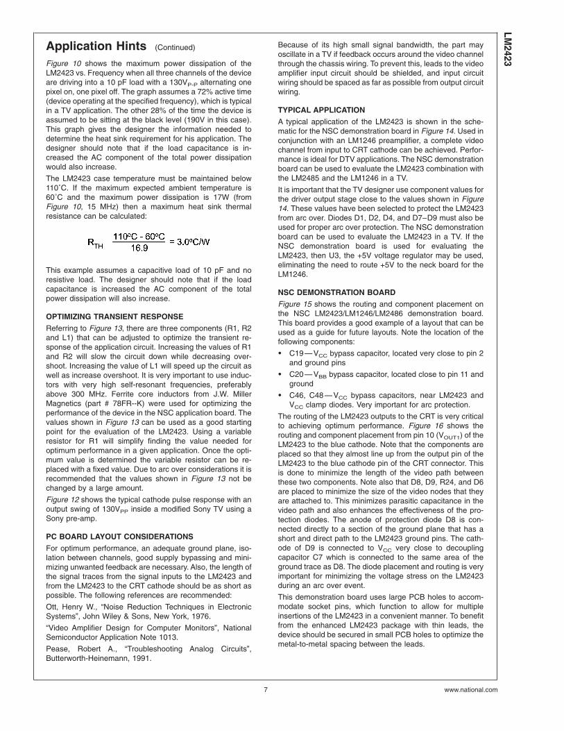
TYPICAL APPLICATION
A typical application of the LM2423 is shown in the sche-matic for the NSC demonstration board in Figure 14. Used inconjunction with an LM1246 preamplifier, a complete videochannel from input to CRT cathode can be achieved. Perfor-mance is ideal for DTV applications. The NSC demonstrationboard can be used to evaluate the LM2423 combination withthe LM2485 and the LM1246 in a TV.
It is important that the TV designer use component values forthe driver output stage close to the values shown in Figure14. These values have been selected to protect the LM2423from arc over. Diodes D1, D2, D4, and D7–D9 must also beused for proper arc over protection. The NSC demonstrationboard can be used to evaluate the LM2423 in a TV. If theNSC demonstration board is used for evaluating theLM2423, then U3, the +5V voltage regulator may be used,eliminating the need to route +5V to the neck board for theLM1246.
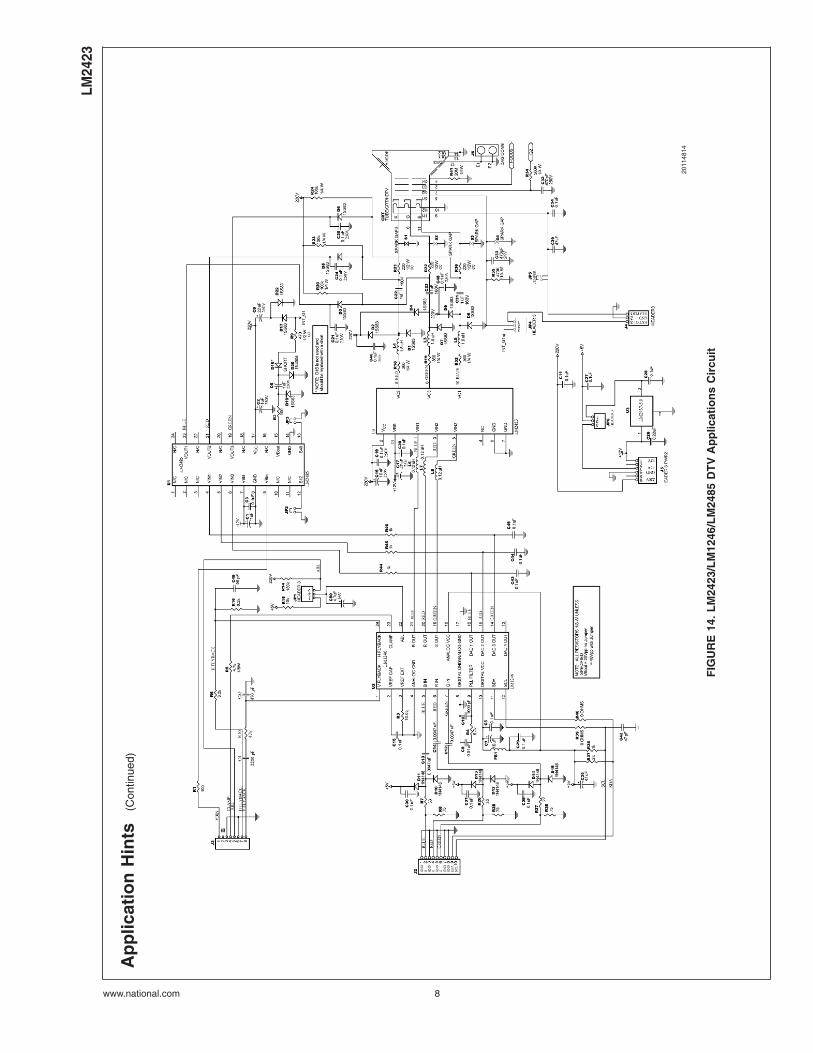
NSC DEMONSTRATION BOARD
Figure 15 shows the routing and component placement onthe NSC LM2423/LM1246/LM2486 demonstration board.This board provides a good example of a layout that can beused as a guide for future layouts. Note the location of thefollowing components:
• C19 — VCC bypass capacitor, located very close to pin 2and ground pins
• C20 — VBB bypass capacitor, located close to pin 11 andground
• C46, C48 — VCC bypass capacitors, near LM2423 andVCC clamp diodes. Very important for arc protection.
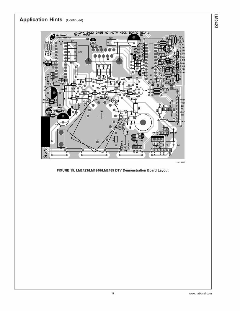
The routing of the LM2423 outputs to the CRT is very criticalto achieving optimum performance. Figure 16 shows therouting and component placement from pin 10 (VOUT1) of theLM2423 to the blue cathode. Note that the components areplaced so that they almost line up from the output pin of theLM2423 to the blue cathode pin of the CRT connector. Thisis done to minimize the length of the video path betweenthese two components. Note also that D8, D9, R24, and D6are placed to minimize the size of the video nodes that theyare attached to. This minimizes parasitic capacitance in thevideo path and also enhances the effectiveness of the pro-tection diodes. The anode of protection diode D8 is con-nected directly to a section of the ground plane that has ashort and direct path to the LM2423 ground pins. The cath-ode of D9 is connected to VCC very close to decouplingcapacitor C7 which is connected to the same area of theground trace as D8. The diode placement and routing is veryimportant for minimizing the voltage stress on the LM2423during an arc over event.
This demonstration board uses large PCB holes to accom-modate socket pins, which function to allow for multipleinsertions of the LM2423 in a convenient manner. To benefitfrom the enhanced LM2423 package with thin leads, thedevice should be secured in small PCB holes to optimize themetal-to-metal spacing between the leads.
LM2423
www.national.com7
Ap
plic
atio
nH
ints
(Con
tinue
d)
2011
4814
FIG
UR
E14
.L
M24
23/L
M12
46/L
M24
85D
TV
Ap
plic
atio
ns
Cir
cuit
LM24
23
www.national.com 8
Application Hints (Continued)
20114816
FIGURE 15. LM2423/LM1246/LM2485 DTV Demonstration Board Layout
LM2423
www.national.com9
Application Hints (Continued)
20114817
FIGURE 16. Trace Routing and Component Placement for Blue Channel Output
LM24
23
www.national.com 10

Physical Dimensions inches (millimeters) unless otherwise noted
NOTE: Available only with lead free plating
NS Package Number TE11BOrder Number LM2423TE NOPB
National does not assume any responsibility for use of any circuitry described, no circuit patent licenses are implied and National reservesthe right at any time without notice to change said circuitry and specifications.
For the most current product information visit us at www.national.com.
LIFE SUPPORT POLICY
NATIONAL’S PRODUCTS ARE NOT AUTHORIZED FOR USE AS CRITICAL COMPONENTS IN LIFE SUPPORT DEVICES OR SYSTEMSWITHOUT THE EXPRESS WRITTEN APPROVAL OF THE PRESIDENT AND GENERAL COUNSEL OF NATIONAL SEMICONDUCTORCORPORATION. As used herein:
1. Life support devices or systems are devices or systemswhich, (a) are intended for surgical implant into the body, or(b) support or sustain life, and whose failure to perform whenproperly used in accordance with instructions for useprovided in the labeling, can be reasonably expected to resultin a significant injury to the user.
2. A critical component is any component of a life supportdevice or system whose failure to perform can be reasonablyexpected to cause the failure of the life support device orsystem, or to affect its safety or effectiveness.
BANNED SUBSTANCE COMPLIANCE
National Semiconductor manufactures products and uses packing materials that meet the provisions of the Customer ProductsStewardship Specification (CSP-9-111C2) and the Banned Substances and Materials of Interest Specification (CSP-9-111S2) and containno ‘‘Banned Substances’’ as defined in CSP-9-111S2.
Leadfree products are RoHS compliant.
National SemiconductorAmericas CustomerSupport CenterEmail: [email protected]: 1-800-272-9959
National SemiconductorEurope Customer Support Center
Fax: +49 (0) 180-530 85 86Email: [email protected]
Deutsch Tel: +49 (0) 69 9508 6208English Tel: +44 (0) 870 24 0 2171Français Tel: +33 (0) 1 41 91 8790
National SemiconductorAsia Pacific CustomerSupport CenterEmail: [email protected]
National SemiconductorJapan Customer Support CenterFax: 81-3-5639-7507Email: [email protected]: 81-3-5639-7560
www.national.com
LM2423
220VM
onolithicTriple
Channel15
MH
zC
RT
DTV
Driver


![Home [learning.millais.org.uk]learning.millais.org.uk/pluginfile.php/18818/mod... · · 2010-10-27Chemistry (Triple) Physics (Triple) A Tantot; Channel 4 Clipbank; Doddle; Go Science;](https://static.fdocuments.us/doc/165x107/5ab9c7527f8b9ad5338e5a72/home-triple-physics-triple-a-tantot-channel-4-clipbank-doddle-go-science.jpg)


