LM111-N, 211-N, 311-N - TI.com Comparator Check for Samples: LM111-N, LM211-N, LM311-N ... For...
30
LM111-N, LM211-N, LM311-N www.ti.com SNOSBJ1E – MAY 1999 – REVISED MARCH 2013 LM111-N/LM211-N/LM311-N Voltage Comparator Check for Samples: LM111-N, LM211-N, LM311-N Both the inputs and the outputs of the LM111-N, 1FEATURES LM211-N or the LM311-N can be isolated from 2• Operates From Single 5V Supply system ground, and the output can drive loads • Input Current: 150 nA Max. Over Temperature referred to ground, the positive supply or the negative supply. Offset balancing and strobe capability are • Offset Current: 20 nA Max. Over Temperature provided and outputs can be wire OR'ed. Although • Differential Input Voltage Range: ±30V slower than the LM106 and LM710 (200 ns response • Power Consumption: 135 mW at ±15V time vs 40 ns) the devices are also much less prone to spurious oscillations. The LM111-N has the same DESCRIPTION pin configuration as the LM106 and LM710. The LM111-N, LM211-N and LM311-N are voltage The LM211-N is identical to the LM111-N, except that comparators that have input currents nearly a its performance is specified over a −25°C to +85°C thousand times lower than devices like the LM106 or temperature range instead of −55°C to +125°C. The LM710. They are also designed to operate over a LM311-N has a temperature range of 0°C to +70°C. wider range of supply voltages: from standard ±15V op amp supplies down to the single 5V supply used for IC logic. Their output is compatible with RTL, DTL and TTL as well as MOS circuits. Further, they can drive lamps or relays, switching voltages up to 50V at currents as high as 50 mA. Typical Applications NOTE Pin connections shown in Schematic Diagram and Typical Applications are for the LMC TO-99 package. Do Not Ground Strobe Pin. Output is turned off when current is pulled from Strobe Pin. Figure 1. Offset Balancing Figure 2. Strobing 1 Please be aware that an important notice concerning availability, standard warranty, and use in critical applications of Texas Instruments semiconductor products and disclaimers thereto appears at the end of this data sheet. 2All trademarks are the property of their respective owners. PRODUCTION DATA information is current as of publication date. Copyright © 1999–2013, Texas Instruments Incorporated Products conform to specifications per the terms of the Texas Instruments standard warranty. Production processing does not necessarily include testing of all parameters.
Transcript of LM111-N, 211-N, 311-N - TI.com Comparator Check for Samples: LM111-N, LM211-N, LM311-N ... For...

LM111-N, LM211-N, LM311-N
www.ti.com SNOSBJ1E –MAY 1999–REVISED MARCH 2013
LM111-N/LM211-N/LM311-N Voltage ComparatorCheck for Samples: LM111-N, LM211-N, LM311-N
Both the inputs and the outputs of the LM111-N,1FEATURES
LM211-N or the LM311-N can be isolated from2• Operates From Single 5V Supply system ground, and the output can drive loads• Input Current: 150 nA Max. Over Temperature referred to ground, the positive supply or the negative
supply. Offset balancing and strobe capability are• Offset Current: 20 nA Max. Over Temperatureprovided and outputs can be wire OR'ed. Although• Differential Input Voltage Range: ±30V slower than the LM106 and LM710 (200 ns response
• Power Consumption: 135 mW at ±15V time vs 40 ns) the devices are also much less proneto spurious oscillations. The LM111-N has the same
DESCRIPTION pin configuration as the LM106 and LM710.The LM111-N, LM211-N and LM311-N are voltage The LM211-N is identical to the LM111-N, except thatcomparators that have input currents nearly a its performance is specified over a −25°C to +85°Cthousand times lower than devices like the LM106 or temperature range instead of −55°C to +125°C. TheLM710. They are also designed to operate over a LM311-N has a temperature range of 0°C to +70°C.wider range of supply voltages: from standard ±15Vop amp supplies down to the single 5V supply usedfor IC logic. Their output is compatible with RTL, DTLand TTL as well as MOS circuits. Further, they candrive lamps or relays, switching voltages up to 50V atcurrents as high as 50 mA.
Typical Applications
NOTEPin connections shown in Schematic Diagram and Typical Applications are for the LMCTO-99 package.
Do Not Ground Strobe Pin. Output is turned off when current ispulled from Strobe Pin.
Figure 1. Offset Balancing Figure 2. Strobing
1
Please be aware that an important notice concerning availability, standard warranty, and use in critical applications ofTexas Instruments semiconductor products and disclaimers thereto appears at the end of this data sheet.
2All trademarks are the property of their respective owners.
PRODUCTION DATA information is current as of publication date. Copyright © 1999–2013, Texas Instruments IncorporatedProducts conform to specifications per the terms of the TexasInstruments standard warranty. Production processing does notnecessarily include testing of all parameters.
LM111-N, LM211-N, LM311-N
SNOSBJ1E –MAY 1999–REVISED MARCH 2013 www.ti.com
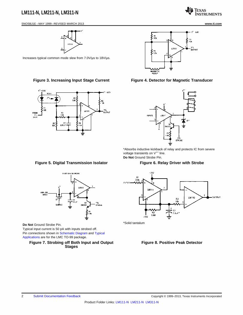
Increases typical common mode slew from 7.0V/μs to 18V/μs.
Figure 3. Increasing Input Stage Current Figure 4. Detector for Magnetic Transducer
*Absorbs inductive kickback of relay and protects IC from severevoltage transients on V++ line.Do Not Ground Strobe Pin.
Figure 5. Digital Transmission Isolator Figure 6. Relay Driver with Strobe
*Solid tantalumDo Not Ground Strobe Pin.Typical input current is 50 pA with inputs strobed off.Pin connections shown in Schematic Diagram and TypicalApplications are for the LMC TO-99 package.
Figure 7. Strobing off Both Input and Output Figure 8. Positive Peak DetectorStages
2 Submit Documentation Feedback Copyright © 1999–2013, Texas Instruments Incorporated
Product Folder Links: LM111-N LM211-N LM311-N
LM111-N, LM211-N, LM311-N
www.ti.com SNOSBJ1E –MAY 1999–REVISED MARCH 2013
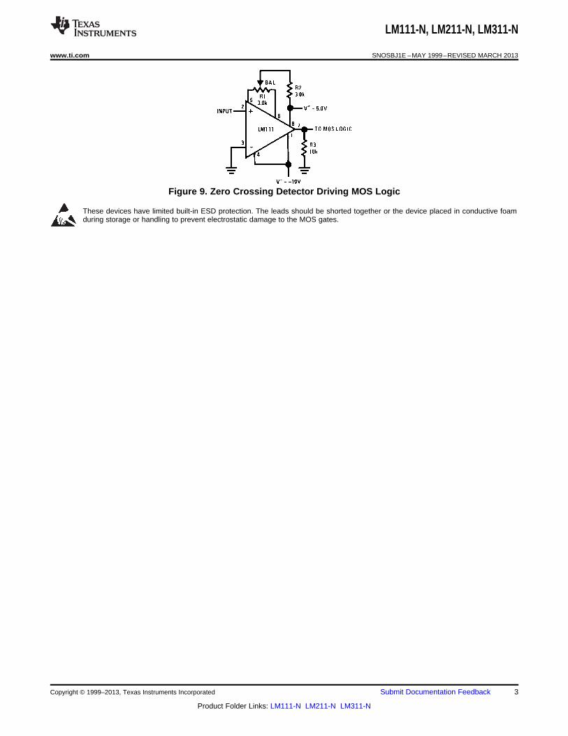
Figure 9. Zero Crossing Detector Driving MOS Logic
These devices have limited built-in ESD protection. The leads should be shorted together or the device placed in conductive foamduring storage or handling to prevent electrostatic damage to the MOS gates.
Copyright © 1999–2013, Texas Instruments Incorporated Submit Documentation Feedback 3
Product Folder Links: LM111-N LM211-N LM311-N

LM111-N, LM211-N, LM311-N
SNOSBJ1E –MAY 1999–REVISED MARCH 2013 www.ti.com
Absolute Maximum Ratings for the LM111-N/LM211-N (1) (2)
Total Supply Voltage (V84) 36V
Output to Negative Supply Voltage (V74) 50V
Ground to Negative Supply Voltage (V14) 30V
Differential Input Voltage ±30V
Input Voltage (3) ±15V
Output Short Circuit Duration 10 sec
Operating Temperature Range LM111-N −55°C to 125°C
LM211-N −25°C to 85°C
Lead Temperature (Soldering, 10 sec) 260°C
Voltage at Strobe Pin V+−5V
Soldering Information Dual-In-Line Package Soldering (10 seconds) 260°C
Small Outline Package Vapor Phase (60 seconds) 215°C
Infrared (15 seconds) 220°C
ESD Rating (4) 300V
(1) Refer to RETS111X for the LM111H, LM111J and LM111J-8 military specifications.(2) If Military/Aerospace specified devices are required, please contact the Texas Instruments Sales Office/ Distributors for availability and
specifications.(3) This rating applies for ±15 supplies. The positive input voltage limit is 30V above the negative supply. The negative input voltage limit is
equal to the negative supply voltage or 30V below the positive supply, whichever is less.(4) Human body model, 1.5 kΩ in series with 100 pF.
Electrical Characteristics (1) for the LM111-N and LM211-NParameter Conditions Min Typ Max Units
Input Offset Voltage (2) TA=25°C, RS≤50k 0.7 3.0 mV
Input Offset Current TA=25°C 4.0 10 nA
Input Bias Current TA=25°C 60 100 nA
Voltage Gain TA=25°C 40 200 V/mV
Response Time (3) TA=25°C 200 ns
Saturation Voltage VIN≤−5 mV, IOUT=50 mA 0.75 1.5 VTA=25°C
Strobe ON Current (4) TA=25°C 2.0 5.0 mA
Output Leakage Current VIN≥5 mV, VOUT=35V, TA=25°C, 0.2 10 nAISTROBE=3 mA
Input Offset Voltage (2) RS≤50 k 4.0 mV
Input Offset Current (2) 20 nA
Input Bias Current 150 nA
Input Voltage Range V+=15V, V−=−15V, Pin 7 Pull-Up −14.5 13.8-14.7 13.0 VMay Go To 5V
Saturation Voltage V+≥4.5V, V−=0, VIN≤−6 mV, 0.23 0.4 VIOUT≤8 mA
Output Leakage Current VIN≥5 mV, VOUT=35V 0.1 0.5 μA
Positive Supply Current TA=25°C 5.1 6.0 mA
Negative Supply Current TA=25°C 4.1 5.0 mA
(1) These specifications apply for VS=±15V and Ground pin at ground, and −55°C≤TA≤+125°C, unless otherwise stated. With the LM211-N,however, all temperature specifications are limited to −25°C≤TA≤+85°C. The offset voltage, offset current and bias current specificationsapply for any supply voltage from a single 5V supply up to ±15V supplies.
(2) The offset voltages and offset currents given are the maximum values required to drive the output within a volt of either supply with a1 mA load. Thus, these parameters define an error band and take into account the worst-case effects of voltage gain and RS.
(3) The response time specified (see definitions) is for a 100 mV input step with 5 mV overdrive.(4) This specification gives the range of current which must be drawn from the strobe pin to ensure the output is properly disabled. Do not
short the strobe pin to ground; it should be current driven at 3 to 5 mA.
4 Submit Documentation Feedback Copyright © 1999–2013, Texas Instruments Incorporated
Product Folder Links: LM111-N LM211-N LM311-N

LM111-N, LM211-N, LM311-N
www.ti.com SNOSBJ1E –MAY 1999–REVISED MARCH 2013
Absolute Maximum Ratings for the LM311-N (1) (2)
Total Supply Voltage (V84) 36V
Output to Negative Supply Voltage (V74) 40V
Ground to Negative Supply Voltage (V14) 30V
Differential Input Voltage ±30V
Input Voltage (3) ±15V
Power Dissipation (4) 500 mW
ESD Rating (5) 300V
Output Short Circuit Duration 10 sec
Operating Temperature Range 0° to 70°C
Storage Temperature Range −65°C to 150°C
Lead Temperature (soldering, 10 sec) 260°C
Voltage at Strobe Pin V+−5V
Soldering Information Dual-In-Line Package Soldering (10 seconds) 260°C
Small Outline Package Vapor Phase (60 seconds) 215°C
Infrared (15 seconds) 220°C
(1) “Absolute Maximum Ratings indicate limits beyond which damage to the device may occur. Operating Ratings indicate conditions forwhich the device is functional, but do not ensure specific performance limits.”
(2) If Military/Aerospace specified devices are required, please contact the Texas Instruments Sales Office/ Distributors for availability andspecifications.
(3) This rating applies for ±15V supplies. The positive input voltage limit is 30V above the negative supply. The negative input voltage limitis equal to the negative supply voltage or 30V below the positive supply, whichever is less.
(4) The maximum junction temperature of the LM311-N is 110°C. For operating at elevated temperature, devices in the LMC package mustbe derated based on a thermal resistance of 165°C/W, junction to ambient, or 20°C/W, junction to case. The thermal resistance of thedual-in-line package is 100°C/W, junction to ambient.
(5) Human body model, 1.5 kΩ in series with 100 pF.
Electrical Characteristics (1) for the LM311-NParameter Conditions Min Typ Max Units
Input Offset Voltage (2) TA=25°C, RS≤50k 2.0 7.5 mV
Input Offset Current (2) TA=25°C 6.0 50 nA
Input Bias Current TA=25°C 100 250 nA
Voltage Gain TA=25°C 40 200 V/mV
Response Time (3) TA=25°C 200 ns
Saturation Voltage VIN≤−10 mV, IOUT=50 mA , 0.75 1.5 VTA=25°C
Strobe ON Current (4) TA=25°C 2.0 5.0 mA
Output Leakage Current VIN≥10 mV, VOUT=35V TA=25°C, 0.2 50 nAISTROBE=3 mA V− = Pin 1 = −5V
Input Offset Voltage (2) RS≤50K 10 mV
Input Offset Current (2) 70 nA
Input Bias Current 300 nA
Input Voltage Range −14.5 13.8,−14.7 13.0 V
Saturation Voltage V+≥4.5V, V−=0, VIN≤−10 mV, 0.23 0.4 VIOUT≤8 mA
Positive Supply Current TA=25°C 5.1 7.5 mA
Negative Supply Current TA=25°C 4.1 5.0 mA
(1) These specifications apply for VS=±15V and Pin 1 at ground, and 0°C < TA < +70°C, unless otherwise specified. The offset voltage,offset current and bias current specifications apply for any supply voltage from a single 5V supply up to ±15V supplies.
(2) The offset voltages and offset currents given are the maximum values required to drive the output within a volt of either supply with1 mA load. Thus, these parameters define an error band and take into account the worst-case effects of voltage gain and RS.
(3) The response time specified (see definitions) is for a 100 mV input step with 5 mV overdrive.(4) This specification gives the range of current which must be drawn from the strobe pin to ensure the output is properly disabled. Do not
short the strobe pin to ground; it should be current driven at 3 to 5 mA.
Copyright © 1999–2013, Texas Instruments Incorporated Submit Documentation Feedback 5
Product Folder Links: LM111-N LM211-N LM311-N

LM111-N, LM211-N, LM311-N
SNOSBJ1E –MAY 1999–REVISED MARCH 2013 www.ti.com
Typical Performance Characteristics LM111-N/LM211-N
Input Bias Current Input Bias Current
Figure 10. Figure 11.
Input Bias Current Input Bias Current
Figure 12. Figure 13.
Input Bias Current Input Bias Current
Figure 14. Figure 15.
6 Submit Documentation Feedback Copyright © 1999–2013, Texas Instruments Incorporated
Product Folder Links: LM111-N LM211-N LM311-N

LM111-N, LM211-N, LM311-N
www.ti.com SNOSBJ1E –MAY 1999–REVISED MARCH 2013
Typical Performance Characteristics LM111-N/LM211-N (continued)Input Bias Current Input Bias CurrentInput Overdrives Input Overdrives
Figure 16. Figure 17.
Response Time for VariousInput Bias Current Input Overdrives
Figure 18. Figure 19.
Response Time for VariousInput Overdrives Output Limiting Characteristics
Figure 20. Figure 21.
Copyright © 1999–2013, Texas Instruments Incorporated Submit Documentation Feedback 7
Product Folder Links: LM111-N LM211-N LM311-N
LM111-N, LM211-N, LM311-N
SNOSBJ1E –MAY 1999–REVISED MARCH 2013 www.ti.com
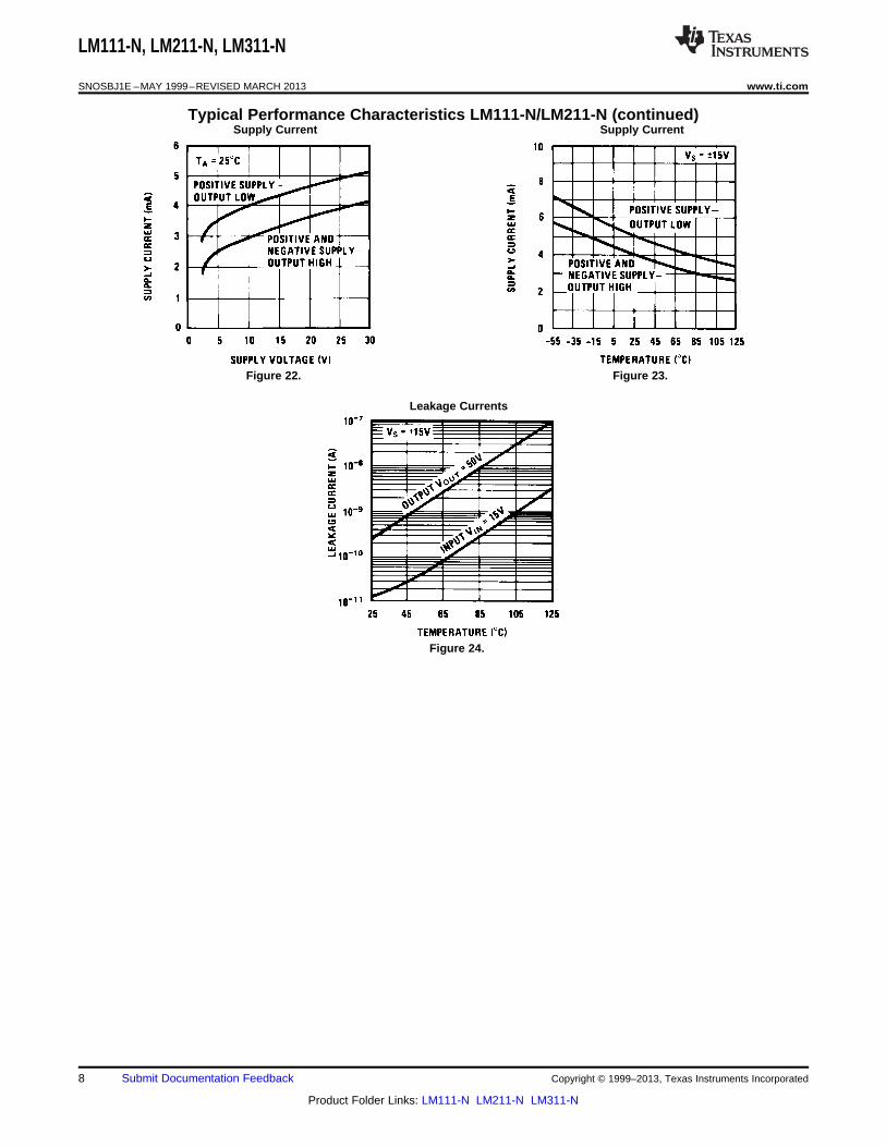
Typical Performance Characteristics LM111-N/LM211-N (continued)Supply Current Supply Current
Figure 22. Figure 23.
Leakage Currents
Figure 24.
8 Submit Documentation Feedback Copyright © 1999–2013, Texas Instruments Incorporated
Product Folder Links: LM111-N LM211-N LM311-N

LM111-N, LM211-N, LM311-N
www.ti.com SNOSBJ1E –MAY 1999–REVISED MARCH 2013
Typical Performance Characteristics LM311-N
Input Bias Current Input Offset Current
Figure 25. Figure 26.
Offset Error Input Characteristics
Figure 27. Figure 28.
Common Mode Limits Transfer Function
Figure 29. Figure 30.
Copyright © 1999–2013, Texas Instruments Incorporated Submit Documentation Feedback 9
Product Folder Links: LM111-N LM211-N LM311-N

LM111-N, LM211-N, LM311-N
SNOSBJ1E –MAY 1999–REVISED MARCH 2013 www.ti.com
Typical Performance Characteristics LM311-N (continued)Response Time for Various Response Time for Various
Input Overdrives Input Overdrives
Figure 31. Figure 32.
Response Time for VariousOutput Saturation Voltage Input Overdrives
Figure 33. Figure 34.
Response Time for VariousInput Overdrives Output Limiting Characteristics
Figure 35. Figure 36.
10 Submit Documentation Feedback Copyright © 1999–2013, Texas Instruments Incorporated
Product Folder Links: LM111-N LM211-N LM311-N

LM111-N, LM211-N, LM311-N
www.ti.com SNOSBJ1E –MAY 1999–REVISED MARCH 2013
Typical Performance Characteristics LM311-N (continued)Supply Current Supply Current
Figure 37. Figure 38.
Leakage Currents
Figure 39.
Copyright © 1999–2013, Texas Instruments Incorporated Submit Documentation Feedback 11
Product Folder Links: LM111-N LM211-N LM311-N

LM111-N, LM211-N, LM311-N
SNOSBJ1E –MAY 1999–REVISED MARCH 2013 www.ti.com
APPLICATION HINTS
CIRCUIT TECHNIQUES FOR AVOIDINGOSCILLATIONS IN COMPARATOR APPLICATIONS
When a high-speed comparator such as the LM111-N is used with fast input signals and low source impedances,the output response will normally be fast and stable, assuming that the power supplies have been bypassed (with0.1 μF disc capacitors), and that the output signal is routed well away from the inputs (pins 2 and 3) and alsoaway from pins 5 and 6.
However, when the input signal is a voltage ramp or a slow sine wave, or if the signal source impedance is high(1 kΩ to 100 kΩ), the comparator may burst into oscillation near the crossing-point. This is due to the high gainand wide bandwidth of comparators like the LM111-N. To avoid oscillation or instability in such a usage, severalprecautions are recommended, as shown in Figure 40 below.1. The trim pins (pins 5 and 6) act as unwanted auxiliary inputs. If these pins are not connected to a trim-pot,
they should be shorted together. If they are connected to a trim-pot, a 0.01 μF capacitor C1 between pins 5and 6 will minimize the susceptibility to AC coupling. A smaller capacitor is used if pin 5 is used for positivefeedback as in Figure 40.
2. Certain sources will produce a cleaner comparator output waveform if a 100 pF to 1000 pF capacitor C2 isconnected directly across the input pins.
3. When the signal source is applied through a resistive network, RS, it is usually advantageous to choose anRS′ of substantially the same value, both for DC and for dynamic (AC) considerations. Carbon, tin-oxide, andmetal-film resistors have all been used successfully in comparator input circuitry. Inductive wirewoundresistors are not suitable.
4. When comparator circuits use input resistors (eg. summing resistors), their value and placement areparticularly important. In all cases the body of the resistor should be close to the device or socket. In otherwords there should be very little lead length or printed-circuit foil run between comparator and resistor toradiate or pick up signals. The same applies to capacitors, pots, etc. For example, if RS=10 kΩ, as little as 5inches of lead between the resistors and the input pins can result in oscillations that are very hard to damp.Twisting these input leads tightly is the only (second best) alternative to placing resistors close to thecomparator.
5. Since feedback to almost any pin of a comparator can result in oscillation, the printed-circuit layout should beengineered thoughtfully. Preferably there should be a groundplane under the LM111-N circuitry, for example,one side of a double-layer circuit card. Ground foil (or, positive supply or negative supply foil) should extendbetween the output and the inputs, to act as a guard. The foil connections for the inputs should be as smalland compact as possible, and should be essentially surrounded by ground foil on all sides, to guard againstcapacitive coupling from any high-level signals (such as the output). If pins 5 and 6 are not used, they shouldbe shorted together. If they are connected to a trim-pot, the trim-pot should be located, at most, a few inchesaway from the LM111-N, and the 0.01 μF capacitor should be installed. If this capacitor cannot be used, ashielding printed-circuit foil may be advisable between pins 6 and 7. The power supply bypass capacitorsshould be located within a couple inches of the LM111-N. (Some other comparators require the power-supplybypass to be located immediately adjacent to the comparator.)
6. It is a standard procedure to use hysteresis (positive feedback) around a comparator, to prevent oscillation,and to avoid excessive noise on the output because the comparator is a good amplifier for its own noise. Inthe circuit of Figure 41, the feedback from the output to the positive input will cause about 3 mV ofhysteresis. However, if RS is larger than 100Ω, such as 50 kΩ, it would not be reasonable to simply increasethe value of the positive feedback resistor above 510 kΩ. The circuit of Figure 42 could be used, but it israther awkward. See the notes in paragraph 7 below.
7. When both inputs of the LM111-N are connected to active signals, or if a high-impedance signal is driving thepositive input of the LM111-N so that positive feedback would be disruptive, the circuit of Figure 40 is ideal.The positive feedback is to pin 5 (one of the offset adjustment pins). It is sufficient to cause 1 to 2 mVhysteresis and sharp transitions with input triangle waves from a few Hz to hundreds of kHz. The positive-feedback signal across the 82Ω resistor swings 240 mV below the positive supply. This signal is centeredaround the nominal voltage at pin 5, so this feedback does not add to the VOS of the comparator. As much as8 mV of VOS can be trimmed out, using the 5 kΩ pot and 3 kΩ resistor as shown.
8. These application notes apply specifically to the LM111-N, LM211-N, LM311-N, and LF111 families ofcomparators, and are applicable to all high-speed comparators in general, (with the exception that not allcomparators have trim pins).
12 Submit Documentation Feedback Copyright © 1999–2013, Texas Instruments Incorporated
Product Folder Links: LM111-N LM211-N LM311-N

LM111-N, LM211-N, LM311-N
www.ti.com SNOSBJ1E –MAY 1999–REVISED MARCH 2013
Pin connections shown are for LM111H in the LMC hermetic package.
Figure 40. Improved Positive Feedback
Pin connections shown are for LM111H in the LMC hermetic package.
Figure 41. Conventional Positive Feedback
Figure 42. Positive Feedback with High Source Resistance
Copyright © 1999–2013, Texas Instruments Incorporated Submit Documentation Feedback 13
Product Folder Links: LM111-N LM211-N LM311-N

LM111-N, LM211-N, LM311-N
SNOSBJ1E –MAY 1999–REVISED MARCH 2013 www.ti.com
Typical Applications
(Pin numbers refer to LMC package)
Figure 43. Zero Crossing Detector Driving MOS Switch
*TTL or DTL fanout of two
Figure 44. 100 kHz Free Running Multivibrator
*Adjust for symmetrical square wave time when VIN = 5 mV
†Minimum capacitance 20 pF Maximum frequency 50 kHz
Figure 45. 10 Hz to 10 kHz Voltage Controlled Oscillator
14 Submit Documentation Feedback Copyright © 1999–2013, Texas Instruments Incorporated
Product Folder Links: LM111-N LM211-N LM311-N

LM111-N, LM211-N, LM311-N
www.ti.com SNOSBJ1E –MAY 1999–REVISED MARCH 2013
*Input polarity is reversed when using pin 1 as output.
Figure 46. Driving Ground-Referred Load
Figure 47. Using Clamp Diodes to Improve Response
*Values shown are for a 0 to 30V logic swing and a 15V threshold.
†May be added to control speed and reduce susceptibility to noise spikes.
Figure 48. TTL Interface with High Level Logic
Figure 49. Crystal Oscillator
Figure 50. Comparator and Solenoid Driver
Copyright © 1999–2013, Texas Instruments Incorporated Submit Documentation Feedback 15
Product Folder Links: LM111-N LM211-N LM311-N

LM111-N, LM211-N, LM311-N
SNOSBJ1E –MAY 1999–REVISED MARCH 2013 www.ti.com
*Solid tantalum
†Adjust to set clamp level
Figure 51. Precision Squarer
*Solid tantalum
Figure 52. Low-Voltage Adjustable Reference Supply
*Solid tantalum
Figure 53. Positive Peak Detector
16 Submit Documentation Feedback Copyright © 1999–2013, Texas Instruments Incorporated
Product Folder Links: LM111-N LM211-N LM311-N

LM111-N, LM211-N, LM311-N
www.ti.com SNOSBJ1E –MAY 1999–REVISED MARCH 2013
Figure 54. Zero Crossing Detector Driving MOS Logic
*Solid tantalum
Figure 55. Negative Peak Detector
*R2 sets the comparison level. At comparison, the photodiode has less than 5 mV across it, decreasing leakages byan order of magnitude.
Figure 56. Precision Photodiode Comparator
Copyright © 1999–2013, Texas Instruments Incorporated Submit Documentation Feedback 17
Product Folder Links: LM111-N LM211-N LM311-N

LM111-N, LM211-N, LM311-N
SNOSBJ1E –MAY 1999–REVISED MARCH 2013 www.ti.com
Figure 57. Switching Power Amplifier
Figure 58. Switching Power Amplifier
18 Submit Documentation Feedback Copyright © 1999–2013, Texas Instruments Incorporated
Product Folder Links: LM111-N LM211-N LM311-N

LM111-N, LM211-N, LM311-N
www.ti.com SNOSBJ1E –MAY 1999–REVISED MARCH 2013
Schematic Diagram
NOTEPin connections shown in the schematic diagram are for the LMC package.
Copyright © 1999–2013, Texas Instruments Incorporated Submit Documentation Feedback 19
Product Folder Links: LM111-N LM211-N LM311-N

LM111-N, LM211-N, LM311-N
SNOSBJ1E –MAY 1999–REVISED MARCH 2013 www.ti.com
Pin Diagrams
Top View
Figure 59. 8-Pin TO-99See LMC Package
Top View Top View
Figure 60. 8-Pin CDIP (See NAB Package) Figure 61. 14-Pin CDIP (See J Package)8-Pin SOIC (See D Package) 14-Pin PDIP (See NFF Package)8-Pin PDIP (See P Package)
Top View
Figure 62. LM111W/883, LM111WG/88310-Pin CLGA (See NAD Package)10-Pin CLGA (See NAC Package)
20 Submit Documentation Feedback Copyright © 1999–2013, Texas Instruments Incorporated
Product Folder Links: LM111-N LM211-N LM311-N
LM111-N, LM211-N, LM311-N
www.ti.com SNOSBJ1E –MAY 1999–REVISED MARCH 2013
REVISION HISTORY
Changes from Revision D (March 2013) to Revision E Page
• Changed layout of National Data Sheet to TI format .......................................................................................................... 20
Copyright © 1999–2013, Texas Instruments Incorporated Submit Documentation Feedback 21
Product Folder Links: LM111-N LM211-N LM311-N

PACKAGE OPTION ADDENDUM
www.ti.com 29-Jun-2017
Addendum-Page 1
PACKAGING INFORMATION
Orderable Device Status(1)
Package Type PackageDrawing
Pins PackageQty
Eco Plan(2)
Lead/Ball Finish(6)
MSL Peak Temp(3)
Op Temp (°C) Device Marking(4/5)
Samples
LM111H ACTIVE TO-99 LMC 8 500 TBD Call TI Call TI -55 to 125 ( LM111H ~ LM111H)
LM111H/NOPB ACTIVE TO-99 LMC 8 500 Green (RoHS& no Sb/Br)
Call TI Level-1-NA-UNLIM -55 to 125 ( LM111H ~ LM111H)
LM111J-8 ACTIVE CDIP NAB 8 40 TBD Call TI Call TI -55 to 125 LM111J-8
LM311M NRND SOIC D 8 95 TBD Call TI Call TI 0 to 70 LM311M
LM311M/NOPB ACTIVE SOIC D 8 95 Green (RoHS& no Sb/Br)
CU SN Level-1-260C-UNLIM 0 to 70 LM311M
LM311MX NRND SOIC D 8 2500 TBD Call TI Call TI 0 to 70 LM311M
LM311MX/NOPB ACTIVE SOIC D 8 2500 Green (RoHS& no Sb/Br)
CU SN Level-1-260C-UNLIM 0 to 70 LM311M
LM311N/NOPB ACTIVE PDIP P 8 40 Green (RoHS& no Sb/Br)
CU SN Level-1-NA-UNLIM 0 to 70 LM311N
(1) The marketing status values are defined as follows:ACTIVE: Product device recommended for new designs.LIFEBUY: TI has announced that the device will be discontinued, and a lifetime-buy period is in effect.NRND: Not recommended for new designs. Device is in production to support existing customers, but TI does not recommend using this part in a new design.PREVIEW: Device has been announced but is not in production. Samples may or may not be available.OBSOLETE: TI has discontinued the production of the device.
(2) RoHS: TI defines "RoHS" to mean semiconductor products that are compliant with the current EU RoHS requirements for all 10 RoHS substances, including the requirement that RoHS substancedo not exceed 0.1% by weight in homogeneous materials. Where designed to be soldered at high temperatures, "RoHS" products are suitable for use in specified lead-free processes. TI mayreference these types of products as "Pb-Free".RoHS Exempt: TI defines "RoHS Exempt" to mean products that contain lead but are compliant with EU RoHS pursuant to a specific EU RoHS exemption.Green: TI defines "Green" to mean the content of Chlorine (Cl) and Bromine (Br) based flame retardants meet JS709B low halogen requirements of <=1000ppm threshold. Antimony trioxide basedflame retardants must also meet the <=1000ppm threshold requirement.
(3) MSL, Peak Temp. - The Moisture Sensitivity Level rating according to the JEDEC industry standard classifications, and peak solder temperature.
(4) There may be additional marking, which relates to the logo, the lot trace code information, or the environmental category on the device.

PACKAGE OPTION ADDENDUM
www.ti.com 29-Jun-2017
Addendum-Page 2
(5) Multiple Device Markings will be inside parentheses. Only one Device Marking contained in parentheses and separated by a "~" will appear on a device. If a line is indented then it is a continuationof the previous line and the two combined represent the entire Device Marking for that device.
(6) Lead/Ball Finish - Orderable Devices may have multiple material finish options. Finish options are separated by a vertical ruled line. Lead/Ball Finish values may wrap to two lines if the finishvalue exceeds the maximum column width.
Important Information and Disclaimer:The information provided on this page represents TI's knowledge and belief as of the date that it is provided. TI bases its knowledge and belief on informationprovided by third parties, and makes no representation or warranty as to the accuracy of such information. Efforts are underway to better integrate information from third parties. TI has taken andcontinues to take reasonable steps to provide representative and accurate information but may not have conducted destructive testing or chemical analysis on incoming materials and chemicals.TI and TI suppliers consider certain information to be proprietary, and thus CAS numbers and other limited information may not be available for release.
In no event shall TI's liability arising out of such information exceed the total purchase price of the TI part(s) at issue in this document sold by TI to Customer on an annual basis.

TAPE AND REEL INFORMATION
*All dimensions are nominal
Device PackageType
PackageDrawing
Pins SPQ ReelDiameter
(mm)
ReelWidth
W1 (mm)
A0(mm)
B0(mm)
K0(mm)
P1(mm)
W(mm)
Pin1Quadrant
LM311MX SOIC D 8 2500 330.0 12.4 6.5 5.4 2.0 8.0 12.0 Q1
LM311MX/NOPB SOIC D 8 2500 330.0 12.4 6.5 5.4 2.0 8.0 12.0 Q1
PACKAGE MATERIALS INFORMATION
www.ti.com 24-Sep-2013
Pack Materials-Page 1

*All dimensions are nominal
Device Package Type Package Drawing Pins SPQ Length (mm) Width (mm) Height (mm)
LM311MX SOIC D 8 2500 367.0 367.0 35.0
LM311MX/NOPB SOIC D 8 2500 367.0 367.0 35.0
PACKAGE MATERIALS INFORMATION
www.ti.com 24-Sep-2013
Pack Materials-Page 2

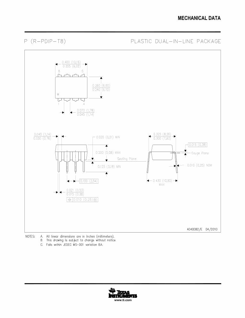
MECHANICAL DATA
NAB0008A
www.ti.com
J08A (Rev M)


IMPORTANT NOTICE
Texas Instruments Incorporated (TI) reserves the right to make corrections, enhancements, improvements and other changes to itssemiconductor products and services per JESD46, latest issue, and to discontinue any product or service per JESD48, latest issue. Buyersshould obtain the latest relevant information before placing orders and should verify that such information is current and complete.TI’s published terms of sale for semiconductor products (http://www.ti.com/sc/docs/stdterms.htm) apply to the sale of packaged integratedcircuit products that TI has qualified and released to market. Additional terms may apply to the use or sale of other types of TI products andservices.Reproduction of significant portions of TI information in TI data sheets is permissible only if reproduction is without alteration and isaccompanied by all associated warranties, conditions, limitations, and notices. TI is not responsible or liable for such reproduceddocumentation. Information of third parties may be subject to additional restrictions. Resale of TI products or services with statementsdifferent from or beyond the parameters stated by TI for that product or service voids all express and any implied warranties for theassociated TI product or service and is an unfair and deceptive business practice. TI is not responsible or liable for any such statements.Buyers and others who are developing systems that incorporate TI products (collectively, “Designers”) understand and agree that Designersremain responsible for using their independent analysis, evaluation and judgment in designing their applications and that Designers havefull and exclusive responsibility to assure the safety of Designers' applications and compliance of their applications (and of all TI productsused in or for Designers’ applications) with all applicable regulations, laws and other applicable requirements. Designer represents that, withrespect to their applications, Designer has all the necessary expertise to create and implement safeguards that (1) anticipate dangerousconsequences of failures, (2) monitor failures and their consequences, and (3) lessen the likelihood of failures that might cause harm andtake appropriate actions. Designer agrees that prior to using or distributing any applications that include TI products, Designer willthoroughly test such applications and the functionality of such TI products as used in such applications.TI’s provision of technical, application or other design advice, quality characterization, reliability data or other services or information,including, but not limited to, reference designs and materials relating to evaluation modules, (collectively, “TI Resources”) are intended toassist designers who are developing applications that incorporate TI products; by downloading, accessing or using TI Resources in anyway, Designer (individually or, if Designer is acting on behalf of a company, Designer’s company) agrees to use any particular TI Resourcesolely for this purpose and subject to the terms of this Notice.TI’s provision of TI Resources does not expand or otherwise alter TI’s applicable published warranties or warranty disclaimers for TIproducts, and no additional obligations or liabilities arise from TI providing such TI Resources. TI reserves the right to make corrections,enhancements, improvements and other changes to its TI Resources. TI has not conducted any testing other than that specificallydescribed in the published documentation for a particular TI Resource.Designer is authorized to use, copy and modify any individual TI Resource only in connection with the development of applications thatinclude the TI product(s) identified in such TI Resource. NO OTHER LICENSE, EXPRESS OR IMPLIED, BY ESTOPPEL OR OTHERWISETO ANY OTHER TI INTELLECTUAL PROPERTY RIGHT, AND NO LICENSE TO ANY TECHNOLOGY OR INTELLECTUAL PROPERTYRIGHT OF TI OR ANY THIRD PARTY IS GRANTED HEREIN, including but not limited to any patent right, copyright, mask work right, orother intellectual property right relating to any combination, machine, or process in which TI products or services are used. Informationregarding or referencing third-party products or services does not constitute a license to use such products or services, or a warranty orendorsement thereof. Use of TI Resources may require a license from a third party under the patents or other intellectual property of thethird party, or a license from TI under the patents or other intellectual property of TI.TI RESOURCES ARE PROVIDED “AS IS” AND WITH ALL FAULTS. TI DISCLAIMS ALL OTHER WARRANTIES ORREPRESENTATIONS, EXPRESS OR IMPLIED, REGARDING RESOURCES OR USE THEREOF, INCLUDING BUT NOT LIMITED TOACCURACY OR COMPLETENESS, TITLE, ANY EPIDEMIC FAILURE WARRANTY AND ANY IMPLIED WARRANTIES OFMERCHANTABILITY, FITNESS FOR A PARTICULAR PURPOSE, AND NON-INFRINGEMENT OF ANY THIRD PARTY INTELLECTUALPROPERTY RIGHTS. TI SHALL NOT BE LIABLE FOR AND SHALL NOT DEFEND OR INDEMNIFY DESIGNER AGAINST ANY CLAIM,INCLUDING BUT NOT LIMITED TO ANY INFRINGEMENT CLAIM THAT RELATES TO OR IS BASED ON ANY COMBINATION OFPRODUCTS EVEN IF DESCRIBED IN TI RESOURCES OR OTHERWISE. IN NO EVENT SHALL TI BE LIABLE FOR ANY ACTUAL,DIRECT, SPECIAL, COLLATERAL, INDIRECT, PUNITIVE, INCIDENTAL, CONSEQUENTIAL OR EXEMPLARY DAMAGES INCONNECTION WITH OR ARISING OUT OF TI RESOURCES OR USE THEREOF, AND REGARDLESS OF WHETHER TI HAS BEENADVISED OF THE POSSIBILITY OF SUCH DAMAGES.Unless TI has explicitly designated an individual product as meeting the requirements of a particular industry standard (e.g., ISO/TS 16949and ISO 26262), TI is not responsible for any failure to meet such industry standard requirements.Where TI specifically promotes products as facilitating functional safety or as compliant with industry functional safety standards, suchproducts are intended to help enable customers to design and create their own applications that meet applicable functional safety standardsand requirements. Using products in an application does not by itself establish any safety features in the application. Designers mustensure compliance with safety-related requirements and standards applicable to their applications. Designer may not use any TI products inlife-critical medical equipment unless authorized officers of the parties have executed a special contract specifically governing such use.Life-critical medical equipment is medical equipment where failure of such equipment would cause serious bodily injury or death (e.g., lifesupport, pacemakers, defibrillators, heart pumps, neurostimulators, and implantables). Such equipment includes, without limitation, allmedical devices identified by the U.S. Food and Drug Administration as Class III devices and equivalent classifications outside the U.S.TI may expressly designate certain products as completing a particular qualification (e.g., Q100, Military Grade, or Enhanced Product).Designers agree that it has the necessary expertise to select the product with the appropriate qualification designation for their applicationsand that proper product selection is at Designers’ own risk. Designers are solely responsible for compliance with all legal and regulatoryrequirements in connection with such selection.Designer will fully indemnify TI and its representatives against any damages, costs, losses, and/or liabilities arising out of Designer’s non-compliance with the terms and provisions of this Notice.
Mailing Address: Texas Instruments, Post Office Box 655303, Dallas, Texas 75265Copyright © 2017, Texas Instruments Incorporated