Lithography overview - TU Grazlamp.tu-graz.ac.at/~hadley/memm/lectures15/mar26.pdfcomplicated...
29
Lithography overview
Transcript of Lithography overview - TU Grazlamp.tu-graz.ac.at/~hadley/memm/lectures15/mar26.pdfcomplicated...

Lithography overview

Optical Lithography
Contact printing, proximity printing with a mask aligner
http://www2.warwick.ac.uk/fac/sci/eng/research/sensors/mbl/facilities/
http://www.lithoguru.com/scientist/lithobasics.html

Optical Lithography
Projection lithography with a stepper or scanner.
http://en.wikipedia.org/wiki/Stepper#/media/File:Scanendnew.gif
http://www.lithoguru.com/scientist/lithobasics.html

http://www.eag.com/mc/sims-ion-beam-sputtering.html#next
Focused ion beam
Secondary Ion Mass Spectroscopy

http://www.wsi.tum.de/Portals/0/Media/Lectures/20082/cb899e9b-2deb-4cb9-bfd5-344821c84fe9/focused_ion_beam_guenthner.pdf
Focused ion beam

Harald Plank, Focused Electron Beam Induced Deposition: from Fundamentals towards Applications, Habilitationsschrift
Focused Electron Beam Induced Deposition (EBID)

Focused ion beam repairs
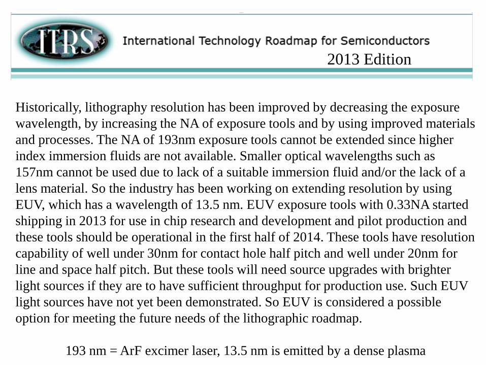
Historically, lithography resolution has been improved by decreasing the exposure wavelength, by increasing the NA of exposure tools and by using improved materials and processes. The NA of 193nm exposure tools cannot be extended since higher index immersion fluids are not available. Smaller optical wavelengths such as 157nm cannot be used due to lack of a suitable immersion fluid and/or the lack of a lens material. So the industry has been working on extending resolution by using EUV, which has a wavelength of 13.5 nm. EUV exposure tools with 0.33NA started shipping in 2013 for use in chip research and development and pilot production and these tools should be operational in the first half of 2014. These tools have resolution capability of well under 30nm for contact hole half pitch and well under 20nm for line and space half pitch. But these tools will need source upgrades with brighter light sources if they are to have sufficient throughput for production use. Such EUV light sources have not yet been demonstrated. So EUV is considered a possible option for meeting the future needs of the lithographic roadmap.
193 nm = ArF excimer laser, 13.5 nm is emitted by a dense plasma
2013 Edition

EUV Lithography
A CO2 laser fires on droplets to molten tin to produce a plasma that emits 13.5 nm photons.
Lens absorb at this wavelength so the light is focused by mirrors.
https://www.cymer.com/euv-lithography/why-lpp

Lenses are not possible. Perfect mirrors required. Air absorbs UV.
https://www.youtube.com/watch?v=8xJEs3a-1QU
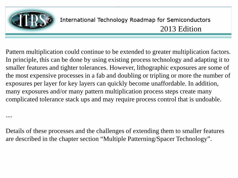
Pattern multiplication could continue to be extended to greater multiplication factors. In principle, this can be done by using existing process technology and adapting it to smaller features and tighter tolerances. However, lithographic exposures are some of the most expensive processes in a fab and doubling or tripling or more the number of exposures per layer for key layers can quickly become unaffordable. In addition, many exposures and/or many pattern multiplication process steps create many complicated tolerance stack ups and may require process control that is undoable.
....
Details of these processes and the challenges of extending them to smaller features are described in the chapter section “Multiple Patterning/Spacer Technology”.
2013 Edition
http://en.wikipedia.org/wiki/Multiple_patterning
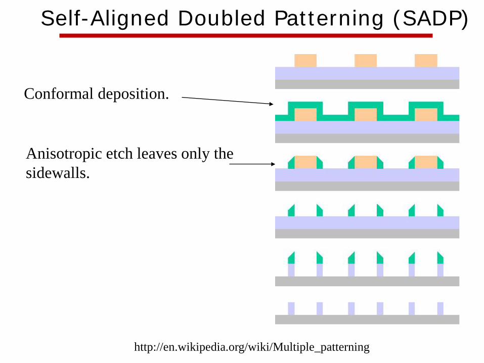
Self-Aligned Doubled Patterning (SADP)
Anisotropic etch leaves only the sidewalls.
Conformal deposition.

E-beam lithography or maskless lithography (ML) uses e-beams to do direct write of features in e-beam sensitive resist. Writing high resolution features with a directed e-beam is intrinsically slow, so in order to get sufficient throughput, massively parallel writing with thousands of independently directed e-beams is necessary. Two different companies are developing tools to do this with a projected delivery date of pilot tools to semiconductor companies of sometime in 2016.
2013 Edition

https://www.youtube.com/watch?feature=player_embedded&v=OQBcDbhw-0Y

Reflective e-beam lithography (REBL) ht
tp://
spie
.org
/x91
889.
xml

Nanoimprint is a potential solution that involves coating a thin pattern of liquid on a wafer and using a mask with high resolution relief patterns to physically stamp the wafer and create a relief pattern. The relief pattern can then be used as an etch mask in much the same way that patterned photoresist is. The leading implementation of this technique using step and flash, where a transparent mask is used to stamp one chip at a time and enable photochemical curing of the patterned material before the stamp is lifted from the wafer. Since this is a contact technique, defects are a significant concerns and a system of master and secondary masks is used to accommodate a short lifetime for the masks used for the actual chip patterning and improve the defectivity of the process.
2013 Edition


video: http://www.joanneum.at/materials/forschungsbereiche/rolle-zu-rolle-nanoimprinten.html
JOANNEUM RESEARCH - MATERIALSRoll-to-Roll Nanoimprint

A patterning technique that has shown a lot of progress in the last two years is directed self-assembly (DSA). This technique takes advantage of the fact that required feature sizes are reaching a size similar to that of polymer molecules that can be readily made in the lab. The most common implementation uses special polymers called block copolymers, which consist of two connected polymers each made from a different monomer. If the monomers are selected properly, the blocks will separate into phase domains when annealed. The phase domains will have a size determined by the size of the individual polymer blocks and the shapes of the domains will be determined by the ratio of the sizes of each polymer block. By creating guiding features on a wafer, this domain formation process can be constrained to give line or hole patterns with the lines and holes in desired locations. Patterns printed with 193nm immersion lithography can be used as guide patterns and pitch multiplication factors of three or four times are readily accessible. This technique was considered a research topic two years ago, but now most major semiconductor producers have substantial programs exploring the possibility of implementing this technique in actual chip production.
2013 Edition

http://en.wikipedia.org/wiki/Multiple_patterning
Directed self-assembly (DSA)
Copolymers such as PMMA/PSform stripe or dot patterns. The positions of the stripes or dots can be guided by topography.

http://en.wikipedia.org/wiki/Silicon#Production
Conversion of silicon into liquids (HSiCl3 or SiCl4) or gases (SiH4). Distillation then the deposition of polysilicon.
Silicon purification
http
://w
ww.
poly
plan
tpro
ject
.com
/imag
es/c
vdre
acto
rs2.
png

images from wikipedia
Czochralski Process
add dopants to the melt
Crystal growth
Cz wafers always contain O, N, C.

Neutron transmutation
30Si + n → 31Si + γ31Si → 31P + β
image from wikipedia
Float zone Process
Fz wafers contain less O, N, C than Cz wafers. Diameter limited.

Silicon wafers
• Cut with a diamond saw• Lapping to remove saw damage• Etching /cleaning to remove lapping damage• Edge rounding for handling• Polishing (fine slurry)• Cleaning: Ammonium Hydroxide - dilute
Hydrofluoric acid - DI water Rinse - Hydrochloric acid and Hydrogen peroxide - DI water rinse.
http://www.processpecialties.com/siliconp.htm

https://www.youtube.com/watch?v=AMgQ1-HdElM
b

Silicon wafers
• Total Thickness Variation: a good 8" Prime wafer would be < 15 µm• Site flatness measurement: < 0.3 µm flatness across each 20×20 mm site.• Bow: < 30 µm concave or convex• Warp: < 20 µm (like a potato chip)• Resistivity variation: 2%-15%
http://www.processpecialties.com/siliconp.htm
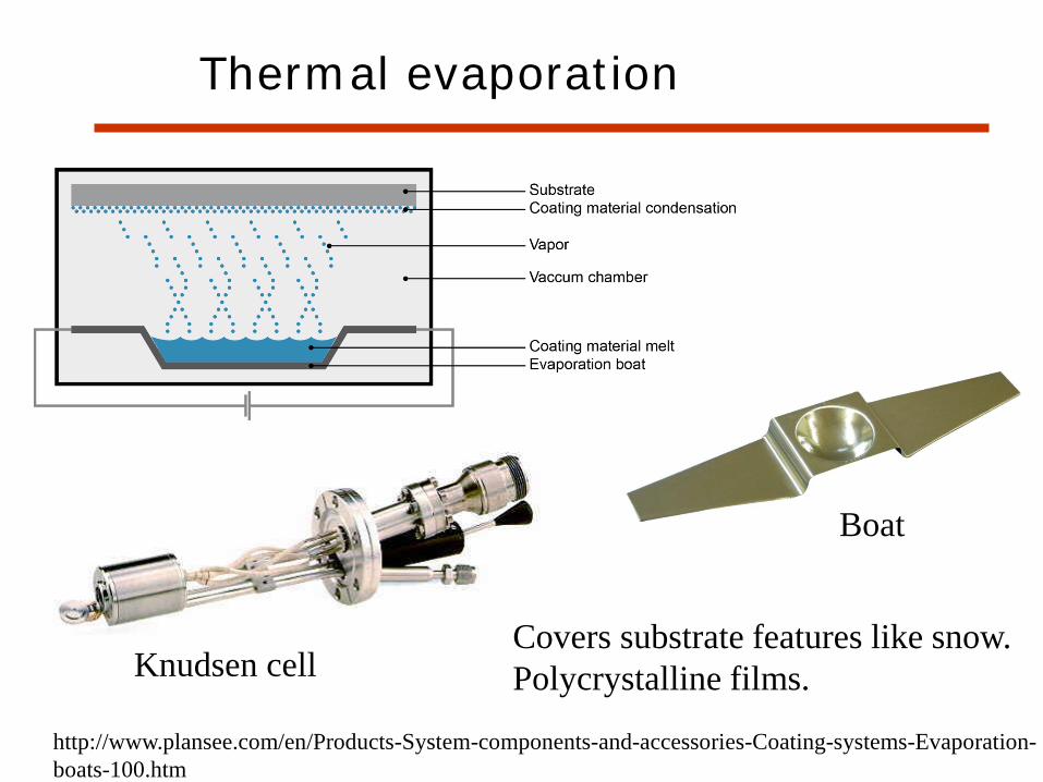
Boat
Thermal evaporation
http://www.plansee.com/en/Products-System-components-and-accessories-Coating-systems-Evaporation-boats-100.htm
Knudsen cellCovers substrate features like snow.Polycrystalline films.

http://www.polyteknik.com/E-Beam_Evaporation.htmlhttp://www.directindustry.com/prod/omicron/evaporators-electron-beam-20757-1062065.html
Electron-beam evaporation

http://www.eps.hw.ac.uk/institutes/photonics-quantum-sciences/mbe.htmhttp://www.fkf.mpg.de/273938/30_Oxide_MBE_Lab
Electron-beam evaporation