Lithographically Patterned Nanoscale Electrodeposition …rcorn/reprints/RMC147.pdf · materials...
8
Lithographically Patterned Nanoscale Electrodeposition of Plasmonic, Bimetallic, Semiconductor, Magnetic, and Polymer Nanoring Arrays Kyunghee Cho, Gabriel Loget, and Robert M. Corn* Department of Chemistry, University of CaliforniaIrvine, Irvine, California 92697, United States ABSTRACT: Large area arrays of magnetic, semiconducting, and insulating nanorings were created by coupling colloidal lithography with nanoscale electrodeposition. This versatile nanoscale fabrication process allows for the independent tuning of the spacing, diameter, and width of the nanorings with typical values of 1.0 μm, 750 nm, and 100 nm, respectively, and was used to form nanorings from a host of materials: Ni, Co, bimetallic Ni/Au, CdSe, and polydopamine. These nanoring arrays have potential applications in memory storage, optical materials, and biosensing. A modified version of this nanoscale electrodeposition process was also used to create arrays of split gold nanorings. The size of the split nanoring opening was controlled by the angle of photoresist exposure during the fabrication process and could be varied from 50% down to 10% of the ring circumference. The large area (cm 2 scale) gold split nanoring array surfaces exhibited strong polarization-dependent plasmonic absorption bands for wavelengths from 1 to 5 μm. Plasmonic nanoscale split ring arrays are potentially useful as tunable dichroic materials throughout the infrared and near-infrared spectral regions. 1. INTRODUCTION The unique physical properties attributed to nanoscale materials have led to a rise of nanomaterials research in recent years. For example, nanopatterned magnetic structures have been studied for applications as varied as high-density data storage to biomedical sensing. 1-4 Semiconducting nanostruc- tures have been developed for quantum confined materials and devices. 5-7 Additionally, plasmonic nanomaterials have received much attention due to their unique optical and electronic properties as well as their potential implementation in a variety of applications including ultrasensitive biosensors, enhanced surface-sensitive spectroscopy, and optical metamaterials. 8-14 Optical metamaterials, defined as periodic structures whose features are smaller than the wavelength of light, can be used to create a variety of unique optical effects: negative refractive index materials, cloaking devices, and perfect lenses. 11,15 The fabrication of nanoring arrays has been of particular interest in nanomaterials research. Magnetic nanorings have been proposed as an ideal candidate for use in random access memory devices due to their well-defined magnetic remnant states, which would be suitable for data storage of multiple bits for each ring. 1,16 Also, the strong plasmonic resonance arising from gold nanorings has been used for detecting polymer film growth and for DNA biosensing. 10 In addition to nanorings, an optical metamaterial that has been the focus of much interest is arrays of split ring resonators, which have been exploited to create materials with negative permeability and negative refractive index in the near-infrared (NIR), infrared (IR), and microwave spectral regions. 17-19 Plasmonic split nanoring arrays exhibit a strongly polarization-dependent absorption spectrum and can be employed for nanophotonic biosensors and plasmonic NIR dichroic polarizing filters. 12,20 In addition, electromagnetic hot spots in the closely related nanocrescent structures have been used in localized surface plasmon resonance based sensing and surface-enhanced spectroscopies (e.g., Raman and infrared absorption). 21-25 Composite plasmonic and magnetic nanocrescents have been employed as surface-enhanced Raman scattering substrates that are capable of being controlled by external magnetic fields. 26 This recent growth in nanotechnology has necessitated the development of facile, inexpensive, and high-throughput processes for the fabrication of nanoscale periodic arrays that are made of a large number of materials. While electron beam lithography (EBL) can be used to generate such nanostructures on the scale of tens to hundreds of microns, 12,18,20,27,28 the time and cost required to fabricate arrays over larger areas using EBL is prohibitive. Alternatively, patterned nanostructures have been fabricated using such methods as nanochannel glass replica membranes, 29,30 colloidal lithography, 31 and evaporative self- assembly. 32 We have recently described a novel method for the fabrication of plasmonic nanoring arrays over large areas (cm 2 ) that combines colloidal lithography with lithographically patterned nanoscale electrodeposition (LPNE). 33 In this paper, we expand the use of this nanofabrication method to make large-scale arrays of nanorings and split nanorings from a wide range of materials, including magnetic Special Issue: John C. Hemminger Festschrift Received: February 19, 2014 Revised: June 16, 2014 Published: June 17, 2014 Article pubs.acs.org/JPCC © 2014 American Chemical Society 28993 dx.doi.org/10.1021/jp501783z | J. Phys. Chem. C 2014, 118, 28993-29000
Transcript of Lithographically Patterned Nanoscale Electrodeposition …rcorn/reprints/RMC147.pdf · materials...

Lithographically Patterned Nanoscale Electrodeposition ofPlasmonic, Bimetallic, Semiconductor, Magnetic, and PolymerNanoring ArraysKyunghee Cho, Gabriel Loget, and Robert M. Corn*
Department of Chemistry, University of CaliforniaIrvine, Irvine, California 92697, United States
ABSTRACT: Large area arrays of magnetic, semiconducting, and insulating nanoringswere created by coupling colloidal lithography with nanoscale electrodeposition. Thisversatile nanoscale fabrication process allows for the independent tuning of the spacing,diameter, and width of the nanorings with typical values of 1.0 μm, 750 nm, and 100nm, respectively, and was used to form nanorings from a host of materials: Ni, Co,bimetallic Ni/Au, CdSe, and polydopamine. These nanoring arrays have potentialapplications in memory storage, optical materials, and biosensing. A modified versionof this nanoscale electrodeposition process was also used to create arrays of split goldnanorings. The size of the split nanoring opening was controlled by the angle ofphotoresist exposure during the fabrication process and could be varied from 50%down to 10% of the ring circumference. The large area (cm2 scale) gold split nanoringarray surfaces exhibited strong polarization-dependent plasmonic absorption bands forwavelengths from 1 to 5 μm. Plasmonic nanoscale split ring arrays are potentially usefulas tunable dichroic materials throughout the infrared and near-infrared spectral regions.
1. INTRODUCTION
The unique physical properties attributed to nanoscalematerials have led to a rise of nanomaterials research in recentyears. For example, nanopatterned magnetic structures havebeen studied for applications as varied as high-density datastorage to biomedical sensing.1−4 Semiconducting nanostruc-tures have been developed for quantum confined materials anddevices.5−7 Additionally, plasmonic nanomaterials have receivedmuch attention due to their unique optical and electronicproperties as well as their potential implementation in a varietyof applications including ultrasensitive biosensors, enhancedsurface-sensitive spectroscopy, and optical metamaterials.8−14
Optical metamaterials, defined as periodic structures whosefeatures are smaller than the wavelength of light, can be used tocreate a variety of unique optical effects: negative refractiveindex materials, cloaking devices, and perfect lenses.11,15
The fabrication of nanoring arrays has been of particularinterest in nanomaterials research. Magnetic nanorings havebeen proposed as an ideal candidate for use in random accessmemory devices due to their well-defined magnetic remnantstates, which would be suitable for data storage of multiple bitsfor each ring.1,16 Also, the strong plasmonic resonance arisingfrom gold nanorings has been used for detecting polymer filmgrowth and for DNA biosensing.10 In addition to nanorings, anoptical metamaterial that has been the focus of much interest isarrays of split ring resonators, which have been exploited tocreate materials with negative permeability and negativerefractive index in the near-infrared (NIR), infrared (IR), andmicrowave spectral regions.17−19 Plasmonic split nanoringarrays exhibit a strongly polarization-dependent absorptionspectrum and can be employed for nanophotonic biosensors
and plasmonic NIR dichroic polarizing filters.12,20 In addition,electromagnetic hot spots in the closely related nanocrescentstructures have been used in localized surface plasmonresonance based sensing and surface-enhanced spectroscopies(e.g., Raman and infrared absorption).21−25 Compositeplasmonic and magnetic nanocrescents have been employedas surface-enhanced Raman scattering substrates that arecapable of being controlled by external magnetic fields.26
This recent growth in nanotechnology has necessitated thedevelopment of facile, inexpensive, and high-throughputprocesses for the fabrication of nanoscale periodic arrays thatare made of a large number of materials. While electron beamlithography (EBL) can be used to generate such nanostructureson the scale of tens to hundreds of microns,12,18,20,27,28 the timeand cost required to fabricate arrays over larger areas using EBLis prohibitive. Alternatively, patterned nanostructures have beenfabricated using such methods as nanochannel glass replicamembranes,29,30 colloidal lithography,31 and evaporative self-assembly.32 We have recently described a novel method for thefabrication of plasmonic nanoring arrays over large areas (cm2)that combines colloidal lithography with lithographicallypatterned nanoscale electrodeposition (LPNE).33
In this paper, we expand the use of this nanofabricationmethod to make large-scale arrays of nanorings and splitnanorings from a wide range of materials, including magnetic
Special Issue: John C. Hemminger Festschrift
Received: February 19, 2014Revised: June 16, 2014Published: June 17, 2014
Article
pubs.acs.org/JPCC
© 2014 American Chemical Society 28993 dx.doi.org/10.1021/jp501783z | J. Phys. Chem. C 2014, 118, 28993−29000

materials (nickel and cobalt), semiconductors (cadmiumselenide), and insulating polymers (polydopamine). Addition-ally, we present bimetallic (nickel/gold) and split gold nanoringarrays as examples of extending our fabrication strategy tocreate more complex nanostructured surfaces. The large areafabrication method described here provides a high degree ofcontrol over nanoscale features such as spacing, radii, thickness,and (in the case of split nanorings) the ring opening size.
2. EXPERIMENTAL SECTION
2.1. Materials. Carboxylate-coated polystyrene beadsolutions (2.6% w/v, 1 μm diameter) were purchased fromPolysciences (Warrington, PA). Shipley S1808 photoresist,Thinner P, and MF-319 developer were purchased fromMicrochem (Newton, MA). Clean Earth Chemicals 24K goldplating solution (Grobet USA, Carlstadt, NJ) was used asreceived. Fisher Premium glass microscope slides (1 mm thick)were used as substrates. Magnetite nanoparticles of 20 nm (20mg/mL in citrate buffer) were purchased from nanoComposix(San Diego, CA) and diluted 1000-fold in water prior to use.2.2. Nanoring and Split Nanoring Array Fabrication. A
densely packed monolayer of polystyrene beads was formed byspin coating polystyrene beads (concentrated to 5.2% in 3:1methanol:water) on hydrophilic oxygen plasma cleaned micro-scope glass slides cut to 2.5 cm × 2.5 cm pieces. Upon drying,the beads were etched in oxygen plasma (200 mTorr, 50 W,−400 VDC, South Bay Technologies, San Clemente, CA) for 5min. A 70 nm layer of Ag (over a 1 nm Cr adhesion layer) wasvapor deposited on top of the etched beads by thermalevaporation. To remove the beads, the samples were sonicatedsequentially in toluene and acentone. Shipley S1808 photoresist(diluted 1:1 with Thinner P) was spin coated on the nanohole
arrays (80 s, 2500 rpm) and baked for 20 min at 90 °C. Thephotoresist was backside exposed through the nanohole arraywith 20 mW/cm2. For split nanoring arrays, the angle ofexposure was controlled by mounting the samples ontotriangular blocks cut to achieve the desired angles. Apotentiostat (PGSTAT12, Metrohm, Riverview, FL) was usedfor electrodeposition. Ni, Co, CdSe, and Au were deposited bypotentiostatic electrodeposition using the following platingconditions: Ni, −0.85 V for 9 min using a Ni plating solution (5mM NiCl2, 5 mM boric acid, 0.1 M KCl); Co, −1.2 V for 2.5min using a Co plating solution (0.14 M CoSO4 and 0.65 Mboric acid); CdSe, −0.64 V for 7 min using a CdSe platingsolution (0.30 M CdSO4, 0.70 mM SeO2, and 0.25 M H2SO4);Au, −0.85 V for 10 min using a commercial gold platingsolution. Polydopamine was deposited by cyclic voltammetry(20 scans at a rate of 20 mV/s; vertex potentials of −0.6 and0.66 V) in a dopamine solution (5 mM dopamine in phosphatebuffer (pH 6.5)). All potentials were measured versus a Ag/AgCl reference electrode; a Pt foil was used as the counter-electrode. After electrodeposition, the photoresist was washedoff with acetone. The Ag sacrificial electrode was removed witha 5% NH4OH and 1% H2O2 etching solution.
2.3. Sample Characterization. SEM: The samples wereimaged on a FEI Magellan scanning electron microscope. XRD:Grazing incidence X-ray diffraction measurements wereperformed on a Rigaku SmartLab X-ray Diffractometer. FT-NIR Absorption Spectra: A Mattson RS-1 FTIR with a halogensource, CaF2 beamsplitter, and InSb detector was used tocapture NIR spectra from 2000 to 10000 cm−1. The beam wasfocused to 3 mm in diameter to interrogate different areas ofthe sample. A bare glass slide was used as the backgroundreference spectrum.
Figure 1. Nanoring and split nanoring array fabrication scheme: (a) polystyrene beads self-assembled in a monolayer are etched to size in an oxygenplasma; (b) nanohole mask is formed by vapor depositing silver over the etched beads and removing the beads; (c) positive photoresist is spincoated onto the nanohole mask. For nanorings: (d) photoresist is backside exposed at normal incidence through the nanoholes; (e) holes are formedin the photoresist upon development; (f) nanorings are electrodeposited onto the exposed silver; and (g) photoresist and silver are removed toreveal nanorings. For split nanorings: (h) exposure at an angle θ leaves part of the nanohole covered by photoresist after (i) development; (j) splitnanoring is electrodeposited through the holes formed in the photoresist to the exposed silver; and (k) split nanorings arrays are completed uponphotoresist and silver removal.
The Journal of Physical Chemistry C Article
dx.doi.org/10.1021/jp501783z | J. Phys. Chem. C 2014, 118, 28993−2900028994

3. RESULTS AND DISCUSSION
3.1. Nanoring and Split Nanoring Array Fabrication.Our method to fabricate magnetic, semiconducting, bimetallic,and insulating nanoring arrays and plasmonic split nanoringarrays (illustrated in Figure 1) is an extension of our previousmethodology for lithographically patterned electrodeposition ofplasmonic nanoring arrays.33 First, carboxylate-functionalizedpolystyrene beads dispersed in a mixture of ethanol and waterare spin-cast onto an oxygen plasma treated glass substrate toform a tightly packed monolayer. The beads are then etched tothe desired size in oxygen plasma (Figure 1a). A sacrificial metalfilm (70 nm silver) is then formed by evaporation depositionover the etched beads, which are subsequently dissolved intoluene, yielding a nanohole array (Figure 1b). Positivephotoresist is then spin coated over the nanohole array (Figure1c). For closed nanoring fabrication, exposure of the photo-resist at normal incidence (Figure 1d) results in completeopening of the nanoholes. In contrast, for split nanoring arrays,exposure at an angle θ from the surface normal (Figure 1h)leaves part of the photoresist unexposed; thus, the holes do notcompletely open upon photoresist development (Figure 1i).During the electrodeposition step (Figure 1f and 1j), with thenanohole array acting as the working electrode, the desiredmaterial can only be deposited on the exposed metal. Thisprocess results in fully closed nanoring arrays when θ = 0°(Figure 1g) or split nanorings when exposed at an angle(Figure 1k) after removal of photoresist and sacrificial metalmaterial.This fabrication method combination offers complete control
over all size parameters of the array. As discussed previously,33
the periodicity of individual split nanorings is determined bythe initial size of the polystyrene beads; the outer diameter iscontrolled by the time exposed to oxygen plasma; and thenanoring thickness and inner diameter are controlled byamount of charge passed during the electrodeposition process.Finally, the nanoring opening size is determined by the
exposure angle θ (θ = 0° for closed rings). The describedmethod produces square centimeter scale arrays of nanoscalestructures while avoiding relatively expensive and time-consuming sequential fabrication processes such as EBL. Inaddition to size and dimensional control, we are able to formnanoring arrays from a broad range of materials available forelectrodeposition.
3.2. Magnetic Nanorings and Nanomushrooms. Usingour combined colloidal lithography and nanoscale electro-deposition process, we have fabricated nanoring arrays ofnickel, a well-known ferromagnetic material. A top-downscanning electron microscope (SEM) image of a Ni nanoringarray formed from 1 μm diameter polystyrene beads is shownin Figure 2a. In addition to simply nickel nanorings, we haveformed composite magnetic and plasmonic nanorings bysequential electrodeposition of nickel and gold (step “g” inFigure 1). By this process, the resulting bimetallic nanoringshave a core of nickel and a shell of gold; the shell does notcompletely envelope the nickel because the outer part of thenickel rings is not available for gold electrodeposition. Weconfirmed this core−shell structure by etching away exposednickel in nitric acid; when compared to the bimetallic structurebefore etching (Figure 2c), a distinct gold lip over where thenickel had been is visible (Figure 2d). Fourier transform near-infrared (FT-NIR) absorbance spectra of nickel and nickel/goldnanoring arrays are depicted in Figure 2b. The nickel spectrumshows a resonance at 5000 cm−1 and a weaker higher-orderresonance at 9000 cm−1. As expected, the addition of a goldshell greatly enhances the resonant response of the nanoringarrays. Interestingly, we see a strong and distinct doubleresonance for our bimetallic nanorings, which likely corre-sponds to two resonances from nickel and gold.In addition to nickel, we have also fabricated magnetic
nanostructures with cobalt. The cobalt deposition wasperformed by potentiostatic electrodeposition in an electrolytecontaining cobalt sulfate and boric acid.34 Successful deposition
Figure 2. (a) Top-down SEM image of the nickel nanoring array. (b) FT-NIR absorbance spectra of nickel (red) and core−shell nickel/gold (blue)nanoring arrays. (c,d) Cross-sectional views of nickel/gold rings before (c) and after (d) etching of nickel in nitric acid. Scale bars: 500 nm.
The Journal of Physical Chemistry C Article
dx.doi.org/10.1021/jp501783z | J. Phys. Chem. C 2014, 118, 28993−2900028995

of cobalt was confirmed by XRD (Figure 3d). While a top-down view (Figure 3a) of the cobalt structures makes the array
appear as tightly packed rings, a tilted view (Figure 3b) on theSEM reveals mushroom-like structures. These “nanomush-rooms” are a result of electrodeposition out of the photoresisthole to the top of the photoresist layer. We tested theferromagnetism of the nanomushrooms by immersing the arrayinto a solution of 20 nm magnetite nanoparticles. Afterthorough rinsing in water and ethanol, followed by dryingunder a nitrogen stream, the studding of the nanomushroomsby the nanoparticles was confirmed by SEM (Figure 3c). Thephysical anisotropy present in these nanomushrooms is difficultto replicate using traditional nanofabrication strategies andopens the door to facile production of similar structures madewith magnetic or nonmagnetic materials.3.3. Semiconducting and Insulating Nanorings. Along
with metallic nanoring arrays, we are also able to fabricatenanorings of semiconducting and insulating materials. As an
example of nanoring arrays of a semiconductor material, weelectrodeposited cadmium selenide by potentiostatic deposition(SEM image shown in Figure 4a) and confirmed the structureby XRD analysis (Figure 4b). Our fabrication method couldprovide a facile and high-throughput route for production ofquantum rings.
Additionally, nanoring arrays of insulating materials havebeen fabricated using this process. We have recently reportedthe electrodeposition of polydopamine (PDA) thin films forpatterning DNA microarray.35 This deposition was performedby repeated cyclic voltammetry (CV) scans at a carefullycontrolled pH. Our nanoring fabrication strategy allows us toscale down PDA electrodeposition to the nanoscale. Figure 5adepicts SEM images of PDA nanorings at two magnifications.While we expect the thickness of these PDA rings to be around3 nm,35 we can see in the inset that the thickness appears to bemuch greater, which we attribute to the collapsing of the PDAstructure upon removal of the sacrificial electrode. As expected,the cathodic and anodic currents in the cyclic voltammogramsdecrease with repeated cycle numbers as the surface becomesmore coated with PDA and thus electrically passivated. As wehave shown previously with macroscale films, these nanoscalePDA ring arrays will allow the development of nanoscalebiosensing platforms.
3.4. Split Nanorings. In addition to forming nanorings of amultitude of materials, our fabrication strategy allows us to alsoproduce split nanorings and control the ring opening size. Goldsplit nanoring arrays were characterized by a combination ofSEM and polarized Fourier transform near-infrared (FT-NIR)spectroscopy. As shown in the SEM image in Figure 6a, thisangled photoexposure process creates an array where the
Figure 3. (a,b) Top-down (a) and tilted (b) SEM images of cobaltnanomushrooms. (c) Cobalt nanomushrooms after immersion in asolution of magnetite nanoparticles. (d) Confirmation by XRD ofcobalt electrodeposition. Scale bars: 1 μm.
Figure 4. SEM image of CdSe nanorings and confirmation of CdSeelectrodeposition by XRD. Scale bar: 1 μm.
The Journal of Physical Chemistry C Article
dx.doi.org/10.1021/jp501783z | J. Phys. Chem. C 2014, 118, 28993−2900028996

openings are all on the same position on the nanorings. Thesize of the nanoring opening can be tuned by varying theexposure angle (θ) of the photoresist, as seen in the SEMimages in Figures 6b−6d. For a given exposure dosage, asmaller θ results in smaller ring openings. As seen in the SEMimages, the ring opening can be controlled to be 50%, 20%, or10% of the ring circumference by exposing at a θ of 45°, 40°,and 35°, respectively.The NIR absorption spectra of these gold split nanoring
arrays were characterized as a function of optical polarizationwith respect to the ring gap orientation. Transmission spectrawere taken with light at normal incidence to the array surface.
In this configuration, the split ring arrays exhibit strong infraredresonances that are dependent on the polarization of theincident light. As seen in Figure 7, two distinct resonances areapparent in the near- to mid-infrared region as the polarizationof the light is varied from φ = 0° (perpendicular to the ringopening; red trace), φ = 30° (orange trace), φ = 60° (greentrace), to φ = 90° (blue trace). Two bands are observed in theoptical spectrum: one at 7400 cm−1 that dominates when φ =0° and the other at 3800 cm−1 that dominates when φ = 90°.These two NIR bands are plasmonic resonances of split
nanoring arrays that have been observed previously.27,28,36−38
The openings in the nanorings break the symmetry of the ring
Figure 5. (a) SEM images of PDA nanorings at low and high (inset) magnifications. (b) Cyclic voltammograms of cycles 1, 3, and 10 during thegrowth of PDA nanorings.
Figure 6. SEM images of nanocrescents and split nanorings. The size of the ring openings decreases with the angle of the backside UV exposure, θ:(a) and (b) θ = 45°, (c) θ = 40°, and (d) θ = 35°.
The Journal of Physical Chemistry C Article
dx.doi.org/10.1021/jp501783z | J. Phys. Chem. C 2014, 118, 28993−2900028997
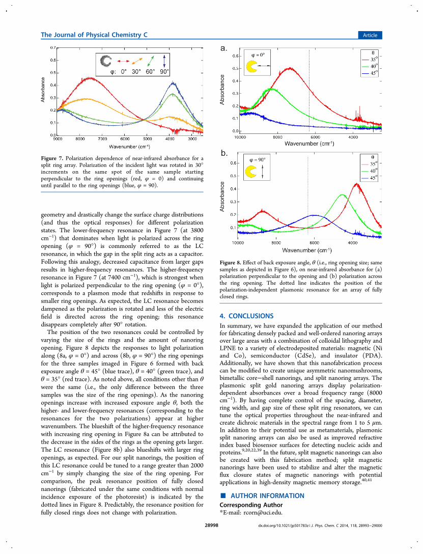
geometry and drastically change the surface charge distributions(and thus the optical responses) for different polarizationstates. The lower-frequency resonance in Figure 7 (at 3800cm−1) that dominates when light is polarized across the ringopening (φ = 90°) is commonly referred to as the LCresonance, in which the gap in the split ring acts as a capacitor.Following this analogy, decreased capacitance from larger gapsresults in higher-frequency resonances. The higher-frequencyresonance in Figure 7 (at 7400 cm−1), which is strongest whenlight is polarized perpendicular to the ring opening (φ = 0°),corresponds to a plasmon mode that redshifts in response tosmaller ring openings. As expected, the LC resonance becomesdampened as the polarization is rotated and less of the electricfield is directed across the ring opening; this resonancedisappears completely after 90° rotation.The position of the two resonances could be controlled by
varying the size of the rings and the amount of nanoringopening. Figure 8 depicts the responses to light polarizationalong (8a, φ = 0°) and across (8b, φ = 90°) the ring openingsfor the three samples imaged in Figure 6 formed with backexposure angle θ = 45° (blue trace), θ = 40° (green trace), andθ = 35° (red trace). As noted above, all conditions other than θwere the same (i.e., the only difference between the threesamples was the size of the ring openings). As the nanoringopenings increase with increased exposure angle θ, both thehigher- and lower-frequency resonances (corresponding to theresonances for the two polarizations) appear at higherwavenumbers. The blueshift of the higher-frequency resonancewith increasing ring opening in Figure 8a can be attributed tothe decrease in the sides of the rings as the opening gets larger.The LC resonance (Figure 8b) also blueshifts with larger ringopenings, as expected. For our split nanorings, the position ofthis LC resonance could be tuned to a range greater than 2000cm−1 by simply changing the size of the ring opening. Forcomparison, the peak resonance position of fully closednanorings (fabricated under the same conditions with normalincidence exposure of the photoresist) is indicated by thedotted lines in Figure 8. Predictably, the resonance position forfully closed rings does not change with polarization.
4. CONCLUSIONSIn summary, we have expanded the application of our methodfor fabricating densely packed and well-ordered nanoring arraysover large areas with a combination of colloidal lithography andLPNE to a variety of electrodeposited materials: magnetic (Niand Co), semiconductor (CdSe), and insulator (PDA).Additionally, we have shown that this nanofabrication processcan be modified to create unique asymmetric nanomushrooms,bimetallic core−shell nanorings, and split nanoring arrays. Theplasmonic split gold nanoring arrays display polarization-dependent absorbances over a broad frequency range (8000cm−1). By having complete control of the spacing, diameter,ring width, and gap size of these split ring resonators, we cantune the optical properties throughout the near-infrared andcreate dichroic materials in the spectral range from 1 to 5 μm.In addition to their potential use as metamaterials, plasmonicsplit nanoring arrays can also be used as improved refractiveindex based biosensor surfaces for detecting nucleic acids andproteins.9,20,22,39 In the future, split magnetic nanorings can alsobe created with this fabrication method; split magneticnanorings have been used to stabilize and alter the magneticflux closure states of magnetic nanorings with potentialapplications in high-density magnetic memory storage.40,41
■ AUTHOR INFORMATIONCorresponding Author*E-mail: [email protected].
Figure 7. Polarization dependence of near-infrared absorbance for asplit ring array. Polarization of the incident light was rotated in 30°increments on the same spot of the same sample startingperpendicular to the ring openings (red, φ = 0) and continuinguntil parallel to the ring openings (blue, φ = 90).
Figure 8. Effect of back exposure angle, θ (i.e., ring opening size; samesamples as depicted in Figure 6), on near-infrared absorbance for (a)polarization perpendicular to the opening and (b) polarization acrossthe ring opening. The dotted line indicates the position of thepolarization-independent plasmonic resonance for an array of fullyclosed rings.
The Journal of Physical Chemistry C Article
dx.doi.org/10.1021/jp501783z | J. Phys. Chem. C 2014, 118, 28993−2900028998

NotesThe authors declare no competing financial interest.
■ ACKNOWLEDGMENTS
The authors thank Dr. Aaron Halpern and Jennifer B. Wood forhelpful discussions. This work was supported by the NIHthrough grant R01-GM059622. SEM and XRD analyses wereperformed at the Laboratory for Electron and X-rayInstrumentation (LEXI) at UC Irvine.
■ REFERENCES(1) Vaz, C. A. F.; Klaui, M.; Heyderman, L. J.; David, C.; Nolting, F.;Bland, J. A. C. Multiplicity of Magnetic Domain States in CircularElements Probed by Photoemission Electron Microscopy. Phys. Rev. B2005, 72, 224426.(2) Miller, M. M.; Prinz, G. A.; Cheng, S.-F.; Bounnak, S. Detectionof a Micron-Sized Magnetic Sphere Using a Ring-Shaped AnisotropicMagnetoresistance-Based Sensor: A Model for a Magnetoresistance-Based Biosensor. Appl. Phys. Lett. 2002, 81, 2211−2213.(3) Klaui, M.; Vaz, C. A. F.; Bland, J. A. C.; Wernsdorfer, W.; Faini,G.; Cambril, E.; Heyderman, L. J. Domain Wall Motion Induced bySpin Polarized Currents in Ferromagnetic Ring Structures. Appl. Phys.Lett. 2003, 83, 105−107.(4) Tang, Z.; Kotov, N. A.; Giersig, M. Spontaneous Organization ofSingle CdTe Nanoparticles into Luminescent Nanowires. Science 2002,297, 237−240.(5) Chen, P.; Chua, S. J.; Wang, Y. D.; Sander, M. D.; Fonstad, C. G.InGaN Nanorings and Nanodots by Selective Area Epitaxy. Appl. Phys.Lett. 2005, 87, 143111.(6) Tian, Y.; Sakr, M. R.; Kinder, J. M.; Liang, D.; MacDonald, M. J.;Qiu, R. J.; Gao, H.; Gao, X. P. A. One-Dimensional QuantumConfinement Effect Modulated Thermoelectric Properties in InAsNanowires. Nano Lett. 2012, 12, 6492−6497.(7) Vayssieres, L.; Sathe, C.; Butorin, S. M.; Shuh, D. K.; Nordgren,J.; Guo, J. One-Dimensional Quantum-Confinement Effect in α-Fe2O3Ultrafine Nanorod Arrays. Adv. Mater. 2005, 17, 2320−2323.(8) Willets, K. A.; Van Duyne, R. P. Localized Surface PlasmonResonance Spectroscopy and Sensing. Annu. Rev. Phys. Chem. 2007,58, 267−297.(9) Huang, C.; Ye, J.; Wang, S.; Stakenborg, T.; Lagae, L. GoldNanoring as a Sensitive Plasmonic Biosensor for On-Chip DNADetection. Appl. Phys. Lett. 2012, 100, 173114.(10) Larsson, E. M.; Alegret, J.; Kall, M.; Sutherland, D. S. SensingCharacteristics of NIR Localized Surface Plasmon Resonances in GoldNanorings for Application as Ultrasensitive Biosensors. Nano Lett.2007, 7, 1256−1263.(11) Alu, A.; Engheta, N. Plasmonic and Metamaterial Cloaking:Physical Mechanisms and Potentials. J. Opt. A: Pure Appl. Opt. 2008,10, 093002.(12) Cao, C.; Zhang, J.; Wen, X.; Dodson, S. L.; Dao, N. T.; Wong,L. M.; Wang, S.; Li, S.; Phan, A. T.; Xiong, Q. Metamaterials-BasedLabel-Free Nanosensor for Conformation and Affinity Biosensing.ACS Nano 2013, 7, 7583−7591.(13) Anker, J. N.; Hall, W. P.; Lyandres, O.; Shah, N. C.; Zhao, J.;Van Duyne, R. P. Biosensing with Plasmonic Nanosensors. Nat. Mater.2008, 7, 442−453.(14) Wang, H.; Brandl, D. W.; Nordlander, P.; Halas, N. PlasmonicNanostructures: Artificial Molecules. Acc. Chem. Res. 2007, 40, 53−62.(15) Liu, N.; Weiss, T.; Mesch, M.; Langguth, L.; Eigenthaler, U.;Hirscher, M.; Sonnichsen, C.; Giessen, H. Planar MetamaterialAnalogue of Electromagnetically Induced Transparency for PlasmonicSensing. Nano Lett. 2010, 10, 1103−1107.(16) Heyderman, L. J.; David, C.; Klaui, M.; Vaz, C. A. F.; Bland, J.Nanoscale Ferromagnetic Rings Fabricated by Electron-BeamLithography. J. Appl. Phys. 2003, 93, 10011−10013.(17) Shelby, R. A.; Smith, D. R.; Schultz, S. Experimental Verificationof a Negative Index of Refraction. Science 2001, 292, 77−79.
(18) Linden, S.; Enkrich, C.; Wegener, M.; Zhou, J.; Koschny, T.;Soukoulis, C. M. Magnetic Response of Metamaterials at 100Terahertz. Science 2004, 306, 1351−1353.(19) Bochenkov, V. E.; Sutherland, D. S. From Rings to Crescents: ANovel Fabrication Technique Uncovers the Transition Details. NanoLett. 2013, 13, 1216−1220.(20) Clark, A. W.; Glidle, A.; Cumming, D. R. S.; Cooper, J. M.Plasmonic Split-Ring Resonators as Dichroic Nanophotonic DNABiosensors. J. Am. Chem. Soc. 2009, 131, 17615−17619.(21) Bukasov, R.; Ali, T. A.; Nordlander, P.; Shumaker-Parry, J. S.Probing the Plasmonic Near-Field of Gold Nanocrescent Antennas.ACS Nano 2010, 4, 6639−6650.(22) Bukasov, R.; Shumaker-Parry, J. S. Highly Tunable InfraredExtinction Properties of Gold Nanocrescents. Nano Lett. 2007, 7,1113−1118.(23) Lewicka, Z. A.; Li, Y.; Bohloul, A.; Yu, W. W.; Colvin, V. L.Nanorings and Nanocrescents Formed via Shaped NanosphereLithography: A Route Toward Large Areas of Infrared Metamaterials.Nanotechnology 2013, 24, 115303−115313.(24) Cataldo, S.; Zhao, J.; Neubrech, F.; Frank, B.; Zhang, C.; Braun,P. V.; Giessen, H. Hole-Mask Colloidal Nano Lithography for Large-Area Low-Cost Metamaterials and Antenna-Assisted Surface-En-hanced Infrared Absorption Substrates. ACS Nano 2012, 6, 979−985.(25) Bukasov, R.; Shumaker-Parry, J. S. Silver Nanocrescents withInfrared Plasmonic Properties as Tunable Substrates for SurfaceEnhanced Infrared Absorption Spectroscopy. Anal. Chem. 2009, 81,4531−4535.(26) Liu, G. L.; Lu, Y.; Kim, J.; Doll, J. C.; Lee, L. P. MagneticNanocrescents as Controllable Surface-Enhanced Raman ScatteringNanoprobes for Biomolecular Imaging. Adv. Mater. 2005, 17, 2683−2688.(27) Clark, A. W.; Sheridan, A. K.; Glidle, A.; Cumming, D. R. S.;Cooper, J. M. Tuneable Visible Resonances in Crescent Shaped Nano-Split-Ring Resonators. Appl. Phys. Lett. 2007, 91, 093109.(28) Rockstuhl, C.; Zentgraf, T.; Guo, H.; Liu, N.; Etrich, C.; Loa, I.;Syassen, K.; Kuhl, J.; Lederer, F.; Giessen, H. Resonances of Split-RingResonator Metamaterials in the Near Infrared. Appl. Phys. B: Laser Opt.2006, 84, 219−227.(29) Pearson, D. H.; Tonucci, R. J. Nanochannel Glass ReplicaMembranes. Science 1995, 270, 68−70.(30) Pearson, D. H.; Tonucci, R. J. Parallel Patterning withNanochannel Glass Replica Membranes. Adv. Mater. 1996, 8, 1031−1034.(31) Zhang, G.; Wang, D. Colloidal Lithography-The Art ofNanochemical Patterning. Chem.Asian J. 2009, 4, 236−245.(32) Lusker, K. L.; Li, J. R.; Garno, J. C. Nanostructures ofFunctionalized Gold Nanoparticles Prepared by Particle Lithographywith Organosilanes. Langmuir 2011, 27, 13269−13275.(33) Halpern, A. R.; Corn, R. M. Lithographically PatternedElectrodeposition of Gold, Silver, and Nickel Nanoring Arrays withWidely Tunable Near-Infrared Plasmonic Resonances. ACS Nano2013, 7, 1755−1762.(34) Kumar, S.; Kumar, R.; Chakarvarti, S. K. Morphological andMagnetic Characterization of Electrodeposited Cobalt Nanowires. J.Mater. Sci. 2004, 39, 2951−2953.(35) Loget, G.; Wood, J. B.; Cho, K.; Halpern, A. R.; Corn, R. M.Electrodeposition of Polydopamine Thin Films for DNA Patterningand Microarrays. Anal. Chem. 2013, 85, 9991−9995.(36) Sheridan, A. K.; Clark, A. W.; Glidle, A.; Cooper, J. M.;Cumming, D. R. S. Multiple Plasmon Resonances from GoldNanostructures. Appl. Phys. Lett. 2007, 90, 143105.(37) Rockstuhl, C.; Lederer, F.; Etrich, C.; Zentgraf, T.; Kuhl, J.;Giessen, H. On the Reinterpretation of Resonances in Split-Ring-Resonators at Normal Incidence. Opt. Express 2006, 14, 8827−8836.(38) Gwinner, M. C.; Koroknay, E.; Fu, L.; Patoka, P.; Kandulski, W.;Giersig, M.; Giessen, H. Periodic Large-Area Metallic Split-RingResonator Metamaterial Fabrication Based on Shadow NanosphereLithography. Small 2009, 5, 400−406.
The Journal of Physical Chemistry C Article
dx.doi.org/10.1021/jp501783z | J. Phys. Chem. C 2014, 118, 28993−2900028999

(39) Liu, S. D.; Zhang, Z. S.; Wang, Q. Q. High Sensitivity and LargeField Enhancement of Symmetry Broken Au Nanorings: Effect ofMultipolar Plasmon Resonance and Propagation. Opt. Express 2009,17, 2906−2917.(40) He, K.; Smith, D. J.; McCartney, M. R. Direct Visualization ofThree-Step Magnetization Reversal of Nanopatterned Spin-ValveElements Using Off-Axis Electron Holography. Appl. Phys. Lett.2009, 94, 172503.(41) Madami, M.; Bisero, D.; Gubbiotti, G.; Tacchi, S.; Carlotti, G.;Nakano, K.; Ono, T. Magnetization Configurations in NiFe SlottedRings Studied by Magneto-Optical Kerr Effect and Magnetic ForceMicroscopy. IEEE Trans. Magn. 2012, 48, 1269−1272.
The Journal of Physical Chemistry C Article
dx.doi.org/10.1021/jp501783z | J. Phys. Chem. C 2014, 118, 28993−2900029000