Lithium Ion Fast-Charge IC datasheet - TI.com · Lithium Ion Fast-Charge IC bq2054 TM Time-out...
23
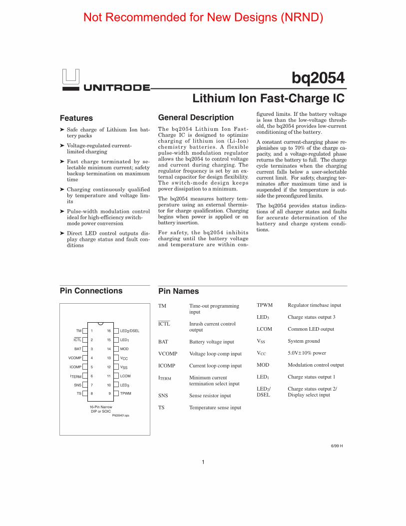
1 Features ➤ Safe charge of Lithium Ion bat- tery packs ➤ Voltage-regulated current- limited charging ➤ Fast charge terminated by se- lectable minimum current; safety backup termination on maximum time ➤ Charging continuously qualified by temperature and voltage lim- its ➤ Pulse-width modulation control ideal for high-efficiency switch- mode power conversion ➤ Direct LED control outputs dis- play charge status and fault con- ditions General Description The bq2054 Lithium Ion Fast- Charge IC is designed to optimize charging of lithium ion (Li-Ion) chemistry batteries. A flexible pulse-width modulation regulator allows the bq2054 to control voltage and current during charging. The regulator frequency is set by an ex- ternal capacitor for design flexibility. The switch-mode design keeps power dissipation to a minimum. The bq2054 measures battery tem- perature using an external thermis- tor for charge qualification. Charging begins when power is applied or on battery insertion. For safety, the bq2054 inhibits charging until the battery voltage and temperature are within con- figured limits. If the battery voltage is less than the low-voltage thresh- old, the bq2054 provides low-current conditioning of the battery. A constant current-charging phase re- plenishes up to 70% of the charge ca- pacity, and a voltage-regulated phase returns the battery to full. The charge cycle terminates when the charging current falls below a user-selectable current limit. For safety, charging ter- minates after maximum time and is suspended if the temperature is out- side the preconfigured limits. The bq2054 provides status indica- tions of all charger states and faults for accurate determination of the battery and charge system condi- tions. Lithium Ion Fast-Charge IC bq2054 TM Time-out programming input ICTL Inrush current control output BAT Battery voltage input VCOMP Voltage loop comp input ICOMP Current loop comp input ITERM Minimum current termination select input SNS Sense resistor input TS Temperature sense input 1 PN205401.eps 16-Pin Narrow DIP or SOIC 2 3 4 5 6 7 8 16 15 14 13 12 11 10 9 LED 2 /DSEL LED 1 MOD V CC V SS LCOM LED 3 TPWM TM ICTL BAT VCOMP ICOMP I TERM SNS TS TPWM Regulator timebase input LED3 Charge status output 3 LCOM Common LED output VSS System ground VCC 5.0V± 10% power MOD Modulation control output LED1 Charge status output 1 LED2/ Charge status output 2/ DSEL Display select input Pin Connections Pin Names 6/99 H Not Recommended for New Designs (NRND)
Transcript of Lithium Ion Fast-Charge IC datasheet - TI.com · Lithium Ion Fast-Charge IC bq2054 TM Time-out...
1
Features Safe charge of Lithium Ion bat-
tery packs
Voltage-regulated current-limited charging
Fast charge terminated by se-lectable minimum current; safetybackup termination on maximumtime
Charging continuously qualifiedby temperature and voltage lim-its
Pulse-width modulation controlideal for high-efficiency switch-mode power conversion
Direct LED control outputs dis-play charge status and fault con-ditions
General DescriptionThe bq2054 Lithium Ion Fast-Charge IC is designed to optimizecharging of lithium ion (Li-Ion)chemistry batteries. A flexiblepulse-width modulation regulatorallows the bq2054 to control voltageand current during charging. Theregulator frequency is set by an ex-ternal capacitor for design flexibility.The switch-mode design keepspower dissipation to a minimum.
The bq2054 measures battery tem-perature using an external thermis-tor for charge qualification. Chargingbegins when power is applied or onbattery insertion.
For safety, the bq2054 inhibitscharging until the battery voltageand temperature are within con-
figured limits. If the battery voltageis less than the low-voltage thresh-old, the bq2054 provides low-currentconditioning of the battery.
A constant current-charging phase re-plenishes up to 70% of the charge ca-pacity, and a voltage-regulated phasereturns the battery to full. The chargecycle terminates when the chargingcurrent falls below a user-selectablecurrent limit. For safety, charging ter-minates after maximum time and issuspended if the temperature is out-side the preconfigured limits.
The bq2054 provides status indica-tions of all charger states and faultsfor accurate determination of thebattery and charge system condi-tions.
Lithium Ion Fast-Charge IC
bq2054
TM Time-out programminginput
ICTL Inrush current controloutput
BAT Battery voltage input
VCOMP Voltage loop comp input
ICOMP Current loop comp input
ITERM Minimum currenttermination select input
SNS Sense resistor input
TS Temperature sense input
1
PN205401.eps
16-Pin NarrowDIP or SOIC
2
3
4
5
6
7
8
16
15
14
13
12
11
10
9
LED2/DSEL
LED1
MOD
VCC
VSS
LCOM
LED3
TPWM
TM
ICTL
BAT
VCOMP
ICOMP
ITERM
SNS
TS
TPWM Regulator timebase input
LED3 Charge status output 3
LCOM Common LED output
VSS System ground
VCC 5.0V±10% power
MOD Modulation control output
LED1 Charge status output 1
LED2/ Charge status output 2/DSEL Display select input
Pin Connections Pin Names
6/99 H
Not Recommended for New Designs (NRND)

Pin DescriptionsTM Time-out programming input
This input sets the maximum charge time.The resistor and capacitor values are deter-mined using Equation 5. Figure 7 shows theresistor/capacitor connection.
ICTL Inrush current control output
ICTL is driven low during the fault orcharge-complete states of the chip. It is usedto disconnect the capacitor across the batterypack terminals, preventing inrush currentsfrom tripping overcurrent protection fea-tures in the pack when a new battery is in-serted.
BAT Battery voltage input
BAT is the battery voltage sense input. Thispotential is generally developed using ahigh-impedance resistor divider networkconnected between the positive and thenegative terminals of the battery. See Fig-ure 4 and Equation 1.
VCOMP Voltage loop compensation input
This input uses an external R-C network forvoltage loop stability.
ITERM Minimum current termination select
This three-state input is used to set IMIN forfast charge termination. See Table 2.
ICOMP Current loop compensation input
This input uses an external R-C network forcurrent loop stability.
SNS Charging current sense input
Battery current is sensed via the voltage de-veloped on this pin by an external sense re-sistor, RSNS, connected in series with thenegative terminal of the battery pack. SeeEquation 6.
TS Temperature sense input
This input is used to monitor battery tempera-ture. An external resistor divider network setsthe lower and upper temperature thresholds.See Figure 6 and Equations 3 and 4.
TPWM Regulation timebase input
This input uses an external timing capacitorto ground to set the pulse-width modulation(PWM) frequency. See Equation 7.
LCOM Common LED output
Common output for LED1–3. This output isin a high-impedance state during initiali-zation to read programming input onDSEL.
MOD Current-switching control output
MOD is a pulse-width modulated push/pulloutput that is used to control the chargingcurrent to the battery. MOD switches highto enable current flow and low to inhibit cur-rent flow.
LED1–LED3
Charger display status 1–3 outputs
These charger status output drivers are forthe direct drive of the LED display. Displaymodes are shown in Table 1. These outputs aretri-stated during initialization so that DSELcan be read.
DSEL Display select input
This three-level input controls the LED1–3charge display modes. See Table 1.
VCC VCC supply
5.0V, ± 10% power
VSS Ground
2
bq2054
Not Recommended for New Designs (NRND)
x0000rjs
Sticky Note
None set by x0000rjs
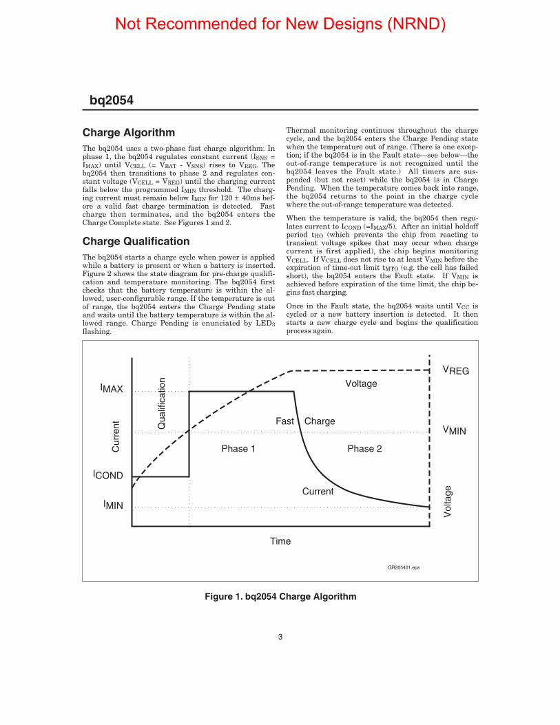
Charge AlgorithmThe bq2054 uses a two-phase fast charge algorithm. Inphase 1, the bq2054 regulates constant current (ISNS =IMAX) until VCELL (= VBAT - VSNS) rises to VREG. Thebq2054 then transitions to phase 2 and regulates con-stant voltage (VCELL = VREG) until the charging currentfalls below the programmed IMIN threshold. The charg-ing current must remain below IMIN for 120 ± 40ms bef-ore a valid fast charge termination is detected. Fastcharge then terminates, and the bq2054 enters theCharge Complete state. See Figures 1 and 2.
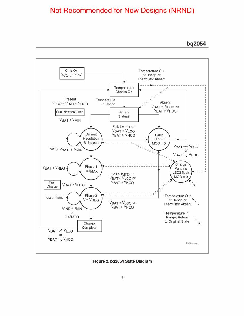
Charge QualificationThe bq2054 starts a charge cycle when power is appliedwhile a battery is present or when a battery is inserted.Figure 2 shows the state diagram for pre-charge qualifi-cation and temperature monitoring. The bq2054 firstchecks that the battery temperature is within the al-lowed, user-configurable range. If the temperature is outof range, the bq2054 enters the Charge Pending stateand waits until the battery temperature is within the al-lowed range. Charge Pending is enunciated by LED3flashing.
Thermal monitoring continues throughout the chargecycle, and the bq2054 enters the Charge Pending statewhen the temperature out of range. (There is one excep-tion; if the bq2054 is in the Fault state—see below—theout-of-range temperature is not recognized until thebq2054 leaves the Fault state.) All timers are sus-pended (but not reset) while the bq2054 is in ChargePending. When the temperature comes back into range,the bq2054 returns to the point in the charge cyclewhere the out-of-range temperature was detected.
When the temperature is valid, the bq2054 then regu-lates current to ICOND (=IMAX/5). After an initial holdoffperiod tHO (which prevents the chip from reacting totransient voltage spikes that may occur when chargecurrent is first applied), the chip begins monitoringVCELL. If VCELL does not rise to at least VMIN before theexpiration of time-out limit tMTO (e.g. the cell has failedshort), the bq2054 enters the Fault state. If VMIN isachieved before expiration of the time limit, the chip be-gins fast charging.
Once in the Fault state, the bq2054 waits until VCC iscycled or a new battery insertion is detected. It thenstarts a new charge cycle and begins the qualificationprocess again.
3
bq2054
GR205401.eps
IMAX
IMIN
ICOND
VMIN
VREG
Cur
rent
Vol
tage
Qua
lific
atio
n
Time
Phase 1 Phase 2
Fast Charge
Voltage
Current
Figure 1. bq2054 Charge Algorithm
Not Recommended for New Designs (NRND)
4
Chip OnVCC 4.5V
TemperatureChecks On
BatteryStatus?
Temperaturein Range
Temperature Outof Range or
Thermistor Absent
Qualification Test
CurrentRegulation@ ICOND
Phase 2V = VREG
FaultLED3 =1 MOD = 0
ChargeComplete
ChargePending
LED3 flashMOD = 0
Phase 1I = IMAX
Temperature Outof Range or
Thermistor Absent
Temperature InRange, Return
to Original State
VBAT < VLCO orVBAT > VHCO
t t > tMTO orVBAT < VLCO orVBAT > VHCO
Fail: t = tQT orVBAT < VLCOVBAT > VHCO
PresentVLCO < VBAT < VHCO
VBAT < VMIN
PASS: VBAT VMIN
VBAT < VREG
VBAT VREGFast
Charge
ISNS > IMIN
ISNS IMINor
t tMTO
FG205401.eps
AbsentVBAT < VLCO or
VBAT > VHCO
>
>
<
>
>
VBAT VLCOor
VBAT VHCO
VBAT VLCOor
VBAT VHCO
Figure 2. bq2054 State Diagram
bq2054
Not Recommended for New Designs (NRND)
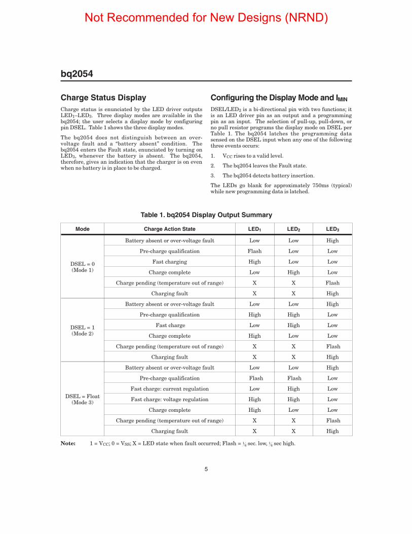
Charge Status DisplayCharge status is enunciated by the LED driver outputsLED1–LED3. Three display modes are available in thebq2054; the user selects a display mode by configuringpin DSEL. Table 1 shows the three display modes.
The bq2054 does not distinguish between an over-voltage fault and a “battery absent” condition. Thebq2054 enters the Fault state, enunciated by turning onLED3, whenever the battery is absent. The bq2054,therefore, gives an indication that the charger is on evenwhen no battery is in place to be charged.
Configuring the Display Mode and IMIN
DSEL/LED2 is a bi-directional pin with two functions; itis an LED driver pin as an output and a programmingpin as an input. The selection of pull-up, pull-down, orno pull resistor programs the display mode on DSEL perTable 1. The bq2054 latches the programming datasensed on the DSEL input when any one of the followingthree events occurs:
1. VCC rises to a valid level.
2. The bq2054 leaves the Fault state.
3. The bq2054 detects battery insertion.
The LEDs go blank for approximately 750ms (typical)while new programming data is latched.
5
bq2054
Mode Charge Action State LED1 LED2 LED3
DSEL = 0(Mode 1)
Battery absent or over-voltage fault Low Low High
Pre-charge qualification Flash Low Low
Fast charging High Low Low
Charge complete Low High Low
Charge pending (temperature out of range) X X Flash
Charging fault X X High
DSEL = 1(Mode 2)
Battery absent or over-voltage fault Low Low High
Pre-charge qualification High High Low
Fast charge Low High Low
Charge complete High Low Low
Charge pending (temperature out of range) X X Flash
Charging fault X X High
DSEL = Float(Mode 3)
Battery absent or over-voltage fault Low Low High
Pre-charge qualification Flash Flash Low
Fast charge: current regulation Low High Low
Fast charge: voltage regulation High High Low
Charge complete High Low Low
Charge pending (temperature out of range) X X Flash
Charging fault X X High
Note: 1 = VCC; 0 = VSS; X = LED state when fault occurred; Flash = 16 sec. low, 1
6 sec high.
Table 1. bq2054 Display Output Summary
Not Recommended for New Designs (NRND)
Fast charge terminates when the charging current dropsbelow a minimum current threshold programmed by thevalue of ITERM (see Table 2) and remains below thatlevel for 120 ± 40ms.
Figure 3 shows the bq2054 configured for display mode 2and IMIN = IMAX/10.
Voltage and Current MonitoringThe bq2054 monitors battery pack voltage at the BATpin. The user must implement a voltage divider be-tween the positive and negative terminals of the batterypack to present a scaled battery pack voltage to the BATpin. The bq2054 also uses the voltage across a sense re-sistor (RSNS) between the negative terminal of the bat-tery pack and ground to monitor the current into thepack. See Figure 4 for the configuration of this network.
The resistor values are calculated from the following:
Equation 1
RB1RB2
N VVREG= −*
.2051
where:
N = Number of cells in series
VREG = Desired fast-charging voltage per cell
These parameters are typically specified by the batterymanufacturer. The total resistance presented across thebattery pack by RB1 + RB2 should be between 150kΩand 1MΩ. The minimum value ensures that the dividernetwork does not drain the battery excessively when thepower source is disconnected. Exceeding the maximumvalue increases the noise susceptibility of the BAT pin.
The current sense resistor, RSNS (see Figure 5), deter-mines the fast charge current. The value of RSNS isgiven by the following:
Equation 2
I VR
MAXSNS
= 0 250.
where:
IMAX = Desired maximum charge current
Hold-Off PeriodBoth VHCO and IMIN terminations are ignored duringthe first 1.33 ± 0.19 seconds of both the Charge Qualifi-cation and Fast Charge phases. This condition preventspremature termination due to voltage spikes that mayoccur when charge is first applied.
6
bq2054
Table 2. IMIN Termination Thresholds
ITERM IMIN
0 IMAX/10
1 IMAX/20
Float IMAX/30
Not Recommended for New Designs (NRND)

7
FG205403.eps
BAT
SNS
bq2054
7
3
13
VCC
12
BAT +
BAT -
VSS
RSNS
RB2
RB1
VSS
VCC
Figure 4. Configuring the Battery Divider
LED2/DSEL
FG205402.eps
LED1
VCC
VSS
LCOM
LED3
bq2054
11
10
12
13
15
16
6
VSS
VCC
10K1K
1K
1K
Figure 3. Configured Display Mode/IMIN Threshold
bq2054
Not Recommended for New Designs (NRND)
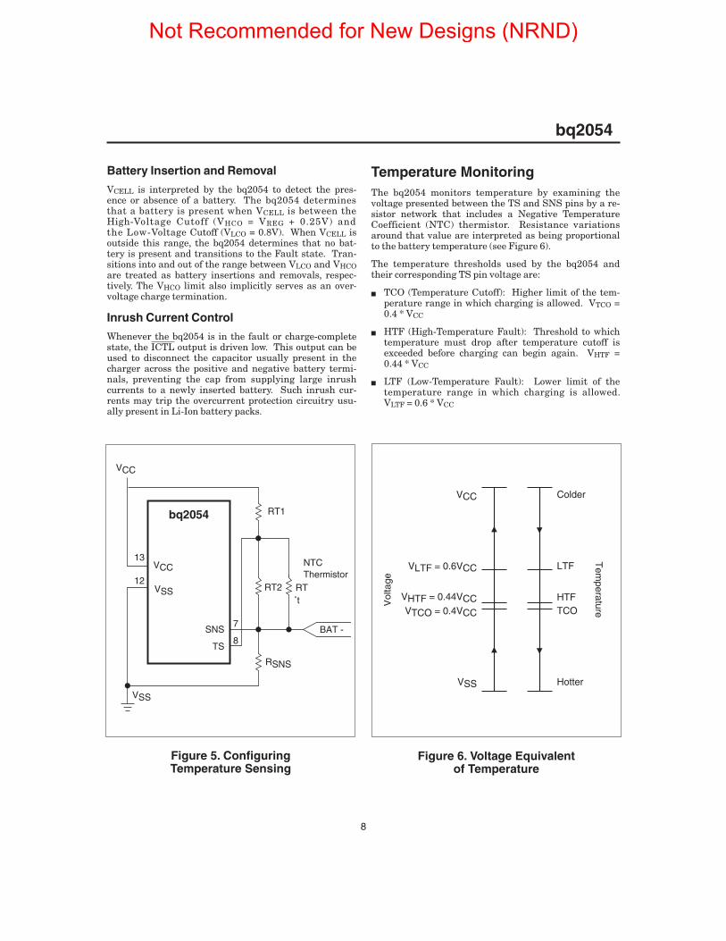
Battery Insertion and Removal
VCELL is interpreted by the bq2054 to detect the pres-ence or absence of a battery. The bq2054 determinesthat a battery is present when VCELL is between theHigh-Voltage Cutoff (VHCO = VREG + 0.25V) andthe Low-Voltage Cutoff (VLCO = 0.8V). When VCELL isoutside this range, the bq2054 determines that no bat-tery is present and transitions to the Fault state. Tran-sitions into and out of the range between VLCO and VHCOare treated as battery insertions and removals, respec-tively. The VHCO limit also implicitly serves as an over-voltage charge termination.
Inrush Current Control
Whenever the bq2054 is in the fault or charge-completestate, the ICTL output is driven low. This output can beused to disconnect the capacitor usually present in thecharger across the positive and negative battery termi-nals, preventing the cap from supplying large inrushcurrents to a newly inserted battery. Such inrush cur-rents may trip the overcurrent protection circuitry usu-ally present in Li-Ion battery packs.
Temperature MonitoringThe bq2054 monitors temperature by examining thevoltage presented between the TS and SNS pins by a re-sistor network that includes a Negative TemperatureCoefficient (NTC) thermistor. Resistance variationsaround that value are interpreted as being proportionalto the battery temperature (see Figure 6).
The temperature thresholds used by the bq2054 andtheir corresponding TS pin voltage are:
TCO (Temperature Cutoff): Higher limit of the tem-perature range in which charging is allowed. VTCO =0.4 * VCC
HTF (High-Temperature Fault): Threshold to whichtemperature must drop after temperature cutoff isexceeded before charging can begin again. VHTF =0.44 * VCC
LTF (Low-Temperature Fault): Lower limit of thetemperature range in which charging is allowed.VLTF = 0.6 * VCC
8
VCC
VLTF = 0.6VCC
VHTF = 0.44VCCVTCO = 0.4VCC
HotterVSS
TCOHTF
LTF
Colder
Vol
tage
Tem
perature
Figure 6. Voltage Equivalentof Temperature
SNS
bq2054
7
13
VCC
12
BAT -
VSS
RSNS
RT2
RT1
VSS
VCC
TS8
˚t
NTCThermistor
RT
Figure 5. ConfiguringTemperature Sensing
bq2054
Not Recommended for New Designs (NRND)
A resistor-divider network can be implemented thatpresents the defined voltage levels to the TS pin at thedesired temperatures (see Figure 6).
The equations for determining RT1 and RT2 are:
Equation 3
0 60 250
1. *
( . )* ( )
( * )
VV
RT1 RT2 RRT2 R
CCCC
LTF
LTF
= −
+ +
Equation 4
0 44 1
1.
* ( )( * )
=+ +RT1 RT2 R
RT2 RHTF
HTF
where:
RLTF = thermistor resistance at LTF
RHTF = thermistor resistance at HTF
TCO is determined by the values of RT1 and RT2. 1%resistors are recommended.
Disabling Temperature Sensing
Temperature sensing can be disabled by placing 10kΩresistors between TS and SNS and between SNS andVCC.
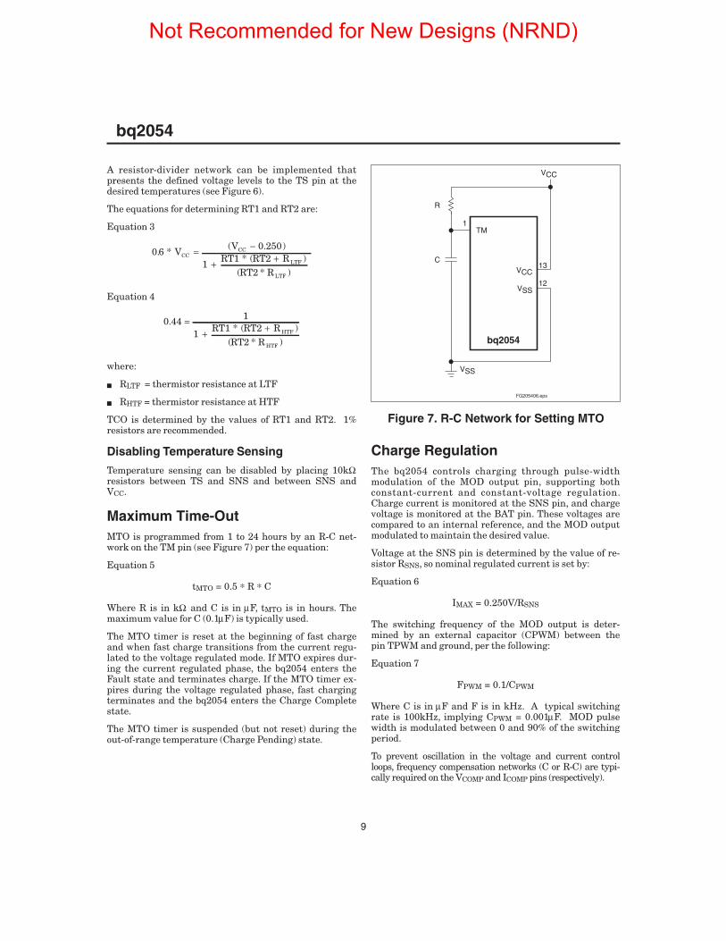
Maximum Time-OutMTO is programmed from 1 to 24 hours by an R-C net-work on the TM pin (see Figure 7) per the equation:
Equation 5
tMTO = 0.5 * R * C
Where R is in kΩ and C is in µF, tMTO is in hours. Themaximum value for C (0.1µF) is typically used.
The MTO timer is reset at the beginning of fast chargeand when fast charge transitions from the current regu-lated to the voltage regulated mode. If MTO expires dur-ing the current regulated phase, the bq2054 enters theFault state and terminates charge. If the MTO timer ex-pires during the voltage regulated phase, fast chargingterminates and the bq2054 enters the Charge Completestate.
The MTO timer is suspended (but not reset) during theout-of-range temperature (Charge Pending) state.
Charge RegulationThe bq2054 controls charging through pulse-widthmodulation of the MOD output pin, supporting bothconstant-current and constant-voltage regulation.Charge current is monitored at the SNS pin, and chargevoltage is monitored at the BAT pin. These voltages arecompared to an internal reference, and the MOD outputmodulated to maintain the desired value.
Voltage at the SNS pin is determined by the value of re-sistor RSNS, so nominal regulated current is set by:
Equation 6
IMAX = 0.250V/RSNS
The switching frequency of the MOD output is deter-mined by an external capacitor (CPWM) between thepin TPWM and ground, per the following:
Equation 7
FPWM = 0.1/CPWM
Where C is in µF and F is in kHz. A typical switchingrate is 100kHz, implying CPWM = 0.001µF. MOD pulsewidth is modulated between 0 and 90% of the switchingperiod.
To prevent oscillation in the voltage and current controlloops, frequency compensation networks (C or R-C) are typi-cally required on the VCOMP and ICOMP pins (respectively).
9
TM
FG205406.eps
VCC
VSS
bq2054
12
13
1
VSS
VCC
C
R
Figure 7. R-C Network for Setting MTO
bq2054
Not Recommended for New Designs (NRND)
10
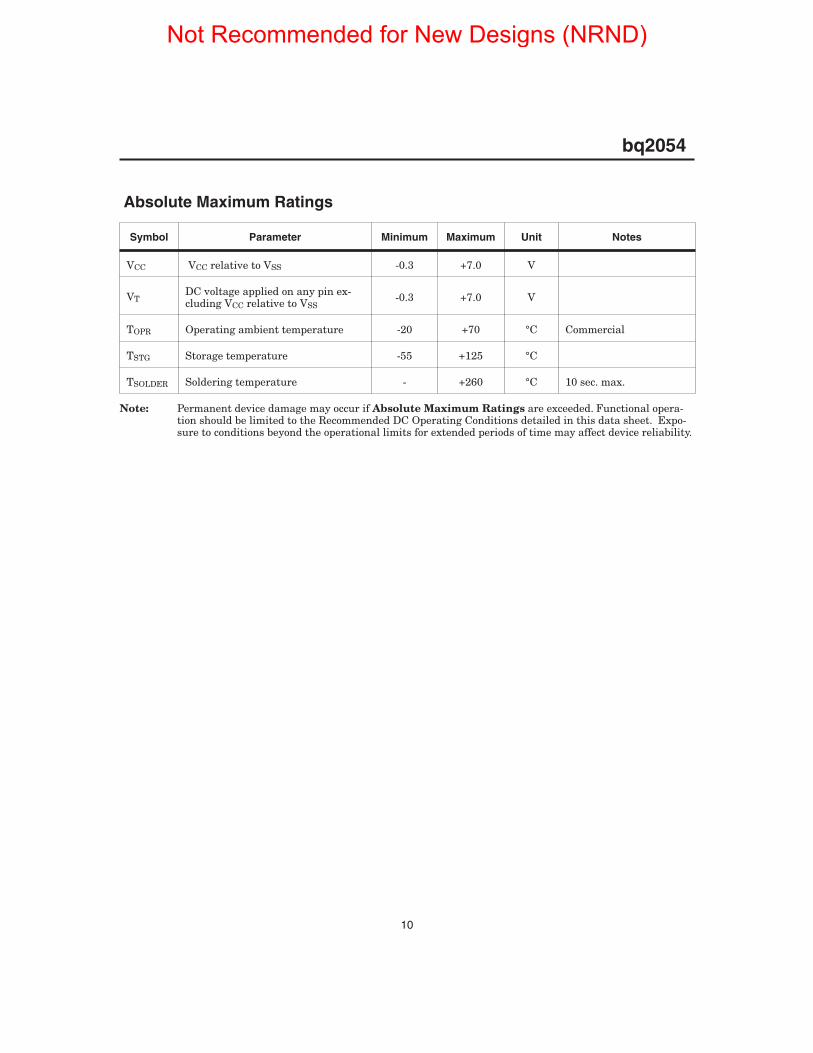
Absolute Maximum Ratings
Symbol Parameter Minimum Maximum Unit Notes
VCC VCC relative to VSS -0.3 +7.0 V
VTDC voltage applied on any pin ex-cluding VCC relative to VSS
-0.3 +7.0 V
TOPR Operating ambient temperature -20 +70 °C Commercial
TSTG Storage temperature -55 +125 °C
TSOLDER Soldering temperature - +260 °C 10 sec. max.
Note: Permanent device damage may occur if Absolute Maximum Ratings are exceeded. Functional opera-tion should be limited to the Recommended DC Operating Conditions detailed in this data sheet. Expo-sure to conditions beyond the operational limits for extended periods of time may affect device reliability.
bq2054
Not Recommended for New Designs (NRND)

11
DC Thresholds (TA = TOPR; VCC = 5V ±10%)
Symbol Parameter Rating Unit Tolerance Notes
VREF
Internal reference voltage 2.05 V 1% TA = 25°C
Temperature coefficient -0.5 mV/°C 10%
VLTF TS maximum threshold 0.6 * VCC V ±0.03V Low-temperature fault
VHTF TS hysteresis threshold 0.44 * VCC V ±0.03V High-temperature fault
VTCO TS minimum threshold 0.4 * VCC V ±0.03V Temperature cutoff
VHCO High cutoff voltage 2.3V V 1%
VMIN Under-voltage threshold at BAT 0.2 * VCC V ±0.03V
VLCO Low cutoff voltage 0.8 V ±0.03V
VSNS Current sense at SNS0.250 V 10% IMAX
0.050 V 10% ICOND
bq2054
Not Recommended for New Designs (NRND)
12
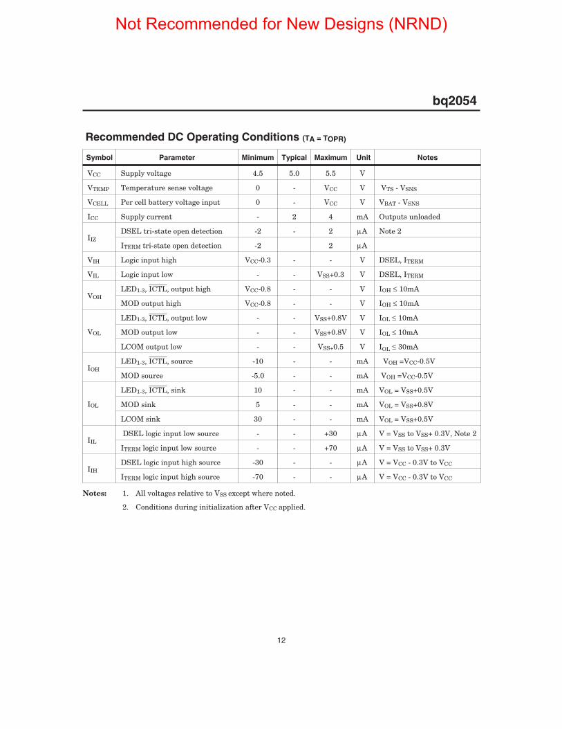
Recommended DC Operating Conditions (TA = TOPR)
Symbol Parameter Minimum Typical Maximum Unit Notes
VCC Supply voltage 4.5 5.0 5.5 V
VTEMP Temperature sense voltage 0 - VCC V VTS - VSNS
VCELL Per cell battery voltage input 0 - VCC V VBAT - VSNS
ICC Supply current - 2 4 mA Outputs unloaded
IIZDSEL tri-state open detection -2 - 2 µA Note 2
ITERM tri-state open detection -2 2 µA
VIH Logic input high VCC-0.3 - - V DSEL, ITERM
VIL Logic input low - - VSS+0.3 V DSEL, ITERM
VOHLED1-3, ICTL, output high VCC-0.8 - - V IOH ≤ 10mA
MOD output high VCC-0.8 - - V IOH ≤ 10mA
VOL
LED1-3, ICTL, output low - - VSS+0.8V V IOL ≤ 10mA
MOD output low - - VSS+0.8V V IOL ≤ 10mA
LCOM output low - - VSS+0.5 V IOL ≤ 30mA
IOHLED1-3, ICTL, source -10 - - mA VOH =VCC-0.5V
MOD source -5.0 - - mA VOH =VCC-0.5V
IOL
LED1-3, ICTL, sink 10 - - mA VOL = VSS+0.5V
MOD sink 5 - - mA VOL = VSS+0.8V
LCOM sink 30 - - mA VOL = VSS+0.5V
IILDSEL logic input low source - - +30 µA V = VSS to VSS+ 0.3V, Note 2
ITERM logic input low source - - +70 µA V = VSS to VSS+ 0.3V
IIHDSEL logic input high source -30 - - µA V = VCC - 0.3V to VCC
ITERM logic input high source -70 - - µA V = VCC - 0.3V to VCC
Notes: 1. All voltages relative to VSS except where noted.
2. Conditions during initialization after VCC applied.
bq2054
Not Recommended for New Designs (NRND)
13
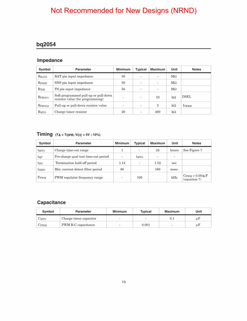
Impedance
Symbol Parameter Minimum Typical Maximum Unit Notes
RBATZ BAT pin input impedance 50 - - MΩ
RSNSZ SNS pin input impedance 50 - - MΩ
RTSZ TS pin input impedance 50 - - MΩ
RPROG1Soft-programmed pull-up or pull-downresistor value (for programming) - - 10 kΩ DSEL
RPROG2 Pull-up or pull-down resistor value - - 3 kΩ ITERM
RMTO Charge timer resistor 20 - 480 kΩ
Timing (TA = TOPR; VCC = 5V ±10%)
Symbol Parameter Minimum Typical Maximum Unit Notes
tMTO Charge time-out range 1 - 24 hours See Figure 7
tQT Pre-charge qual test time-out period - tMTO - -
tHO Termination hold-off period 1.14 - 1.52 sec.
tIMIN Min. current detect filter period 80 160 msec.
FPWM PWM regulator frequency range - 100 kHz CPWM = 0.001µF(equation 7)
Capacitance
Symbol Parameter Minimum Typical Maximum Unit
CMTO Charge timer capacitor - - 0.1 µF
CPWM PWM R-C capacitance - 0.001 - µF
bq2054
Not Recommended for New Designs (NRND)
14
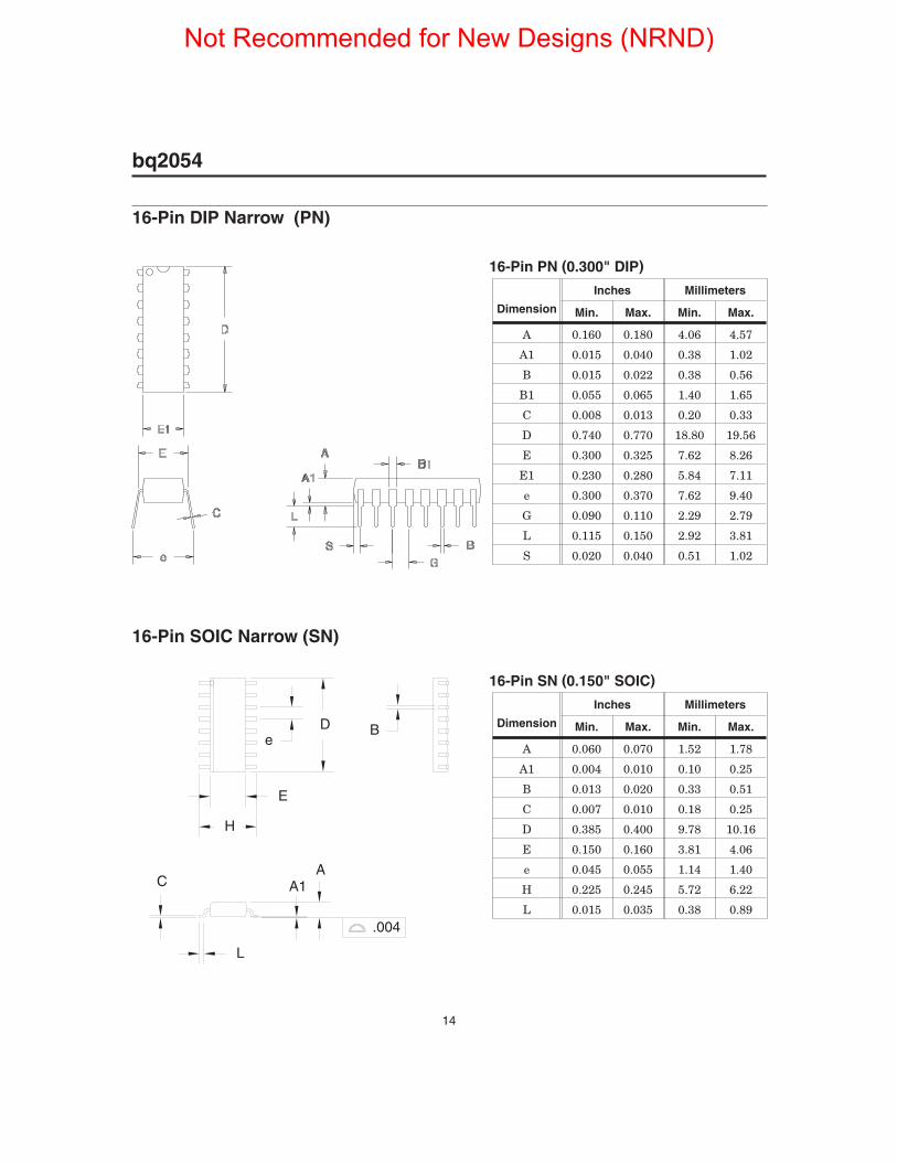
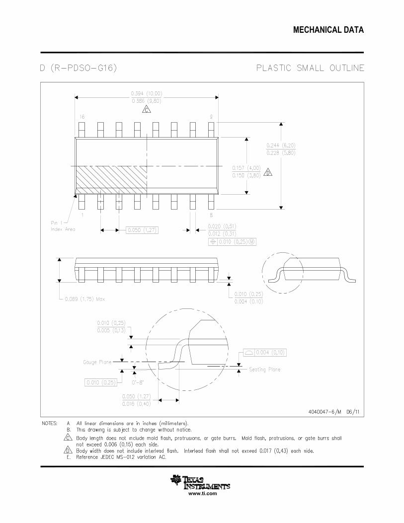
bq2054
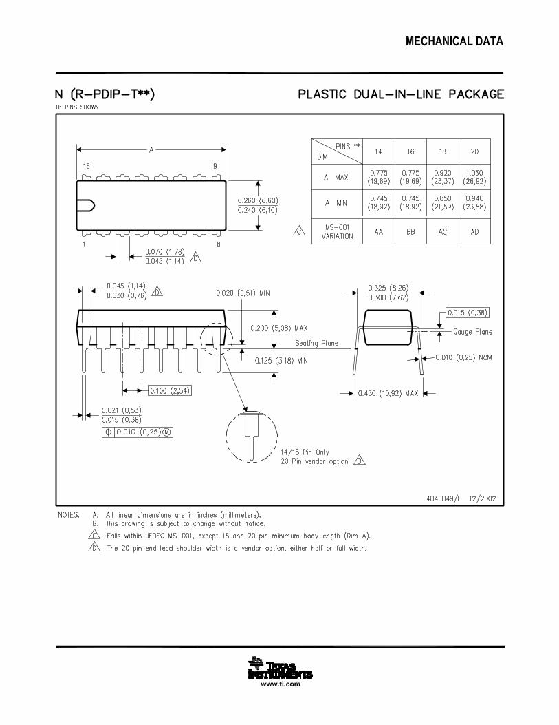
16-Pin PN (0.300" DIP)
Dimension
Inches Millimeters
Min. Max. Min. Max.
A 0.160 0.180 4.06 4.57
A1 0.015 0.040 0.38 1.02
B 0.015 0.022 0.38 0.56
B1 0.055 0.065 1.40 1.65
C 0.008 0.013 0.20 0.33
D 0.740 0.770 18.80 19.56
E 0.300 0.325 7.62 8.26
E1 0.230 0.280 5.84 7.11
e 0.300 0.370 7.62 9.40
G 0.090 0.110 2.29 2.79
L 0.115 0.150 2.92 3.81
S 0.020 0.040 0.51 1.02
16-Pin DIP Narrow (PN)
16-Pin SOIC Narrow (SN)
AA1
.004
C
Be
D
E
H
L
16-Pin SN (0.150" SOIC)
Dimension
Inches Millimeters
Min. Max. Min. Max.
A 0.060 0.070 1.52 1.78
A1 0.004 0.010 0.10 0.25
B 0.013 0.020 0.33 0.51
C 0.007 0.010 0.18 0.25
D 0.385 0.400 9.78 10.16
E 0.150 0.160 3.81 4.06
e 0.045 0.055 1.14 1.40
H 0.225 0.245 5.72 6.22
L 0.015 0.035 0.38 0.89
Not Recommended for New Designs (NRND)

15
bq2054
Data Sheet Revision HistoryChange No. Page No. Description Nature of Change
1 5, 7, 8, 10 Value Change Changed VSNS and IMAX
2 5, 10 Value Change Changed VREF
3 10 Coefficient Addition Temperature coefficient added
4 5 New state diagram Diagram inserted
4 1, 2, 8, 12 NC pin replaced with ICTL
4 3, 5, 13 Termination hold-off period addedIMIN detect filtering added
5 11 VHCO Rating changed to 2.3VVHCO Tolerance changed to 1%
Changed values for VHCO
6 13 tQT in Timing Specifications tQT changed from (0.16 ∗ tMTO) to tMTO
7 5 ITERM in Table 2 Z changes to Float
7 8 Figure 6 RB1 and RB2 changed to RT1 and RT2
8 10 TOPR Deleted industrial temperature range.
Notes: Change 3 = April 1996 C changes from Dec. 1995 B.Change 4 = Sept. 1996 D changes from April 1996 C.Change 5 = Nov. 1996 E changes from Sept. 1996 D.Change 6 = Oct. 1997 F changes from Nov. 1996 E.Change 7 = Oct. 1997 G changes from Oct. 1997 F.Change 8 = June 1999 H changes from Oct. 1997 G.
Ordering Information
bq2054
Package Option:PN = 16-pin plastic DIPSN = 16-pin narrow SOIC
Device:bq2054 Li-Ion Fast-Charge IC
Not Recommended for New Designs (NRND)
PACKAGE OPTION ADDENDUM
www.ti.com 2-Apr-2018
Addendum-Page 1
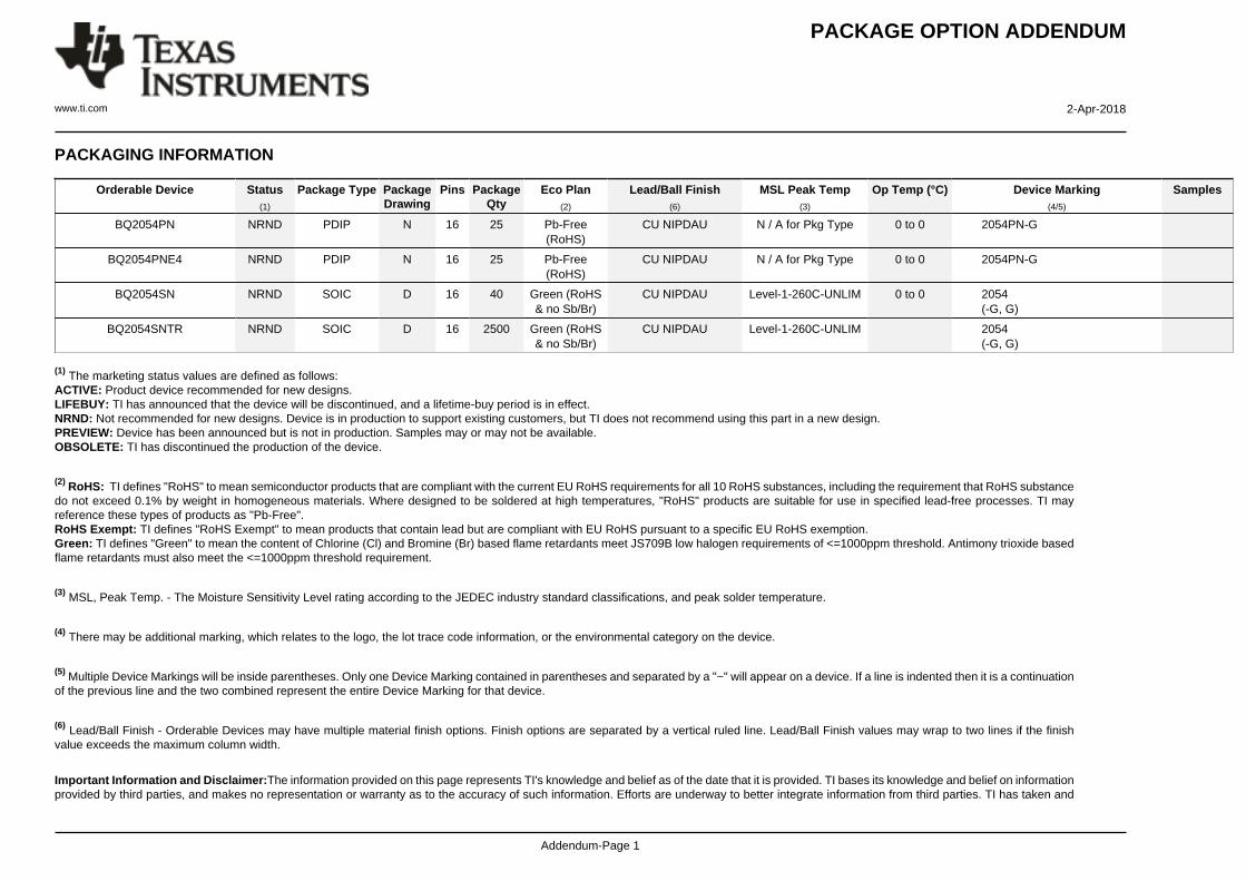
PACKAGING INFORMATION
Orderable Device Status(1)
Package Type PackageDrawing
Pins PackageQty
Eco Plan(2)
Lead/Ball Finish(6)
MSL Peak Temp(3)
Op Temp (°C) Device Marking(4/5)
Samples
BQ2054PN NRND PDIP N 16 25 Pb-Free(RoHS)
CU NIPDAU N / A for Pkg Type 0 to 0 2054PN-G
BQ2054PNE4 NRND PDIP N 16 25 Pb-Free(RoHS)
CU NIPDAU N / A for Pkg Type 0 to 0 2054PN-G
BQ2054SN NRND SOIC D 16 40 Green (RoHS& no Sb/Br)
CU NIPDAU Level-1-260C-UNLIM 0 to 0 2054(-G, G)
BQ2054SNTR NRND SOIC D 16 2500 Green (RoHS& no Sb/Br)
CU NIPDAU Level-1-260C-UNLIM 2054(-G, G)
(1) The marketing status values are defined as follows:ACTIVE: Product device recommended for new designs.LIFEBUY: TI has announced that the device will be discontinued, and a lifetime-buy period is in effect.NRND: Not recommended for new designs. Device is in production to support existing customers, but TI does not recommend using this part in a new design.PREVIEW: Device has been announced but is not in production. Samples may or may not be available.OBSOLETE: TI has discontinued the production of the device.
(2) RoHS: TI defines "RoHS" to mean semiconductor products that are compliant with the current EU RoHS requirements for all 10 RoHS substances, including the requirement that RoHS substancedo not exceed 0.1% by weight in homogeneous materials. Where designed to be soldered at high temperatures, "RoHS" products are suitable for use in specified lead-free processes. TI mayreference these types of products as "Pb-Free".RoHS Exempt: TI defines "RoHS Exempt" to mean products that contain lead but are compliant with EU RoHS pursuant to a specific EU RoHS exemption.Green: TI defines "Green" to mean the content of Chlorine (Cl) and Bromine (Br) based flame retardants meet JS709B low halogen requirements of <=1000ppm threshold. Antimony trioxide basedflame retardants must also meet the <=1000ppm threshold requirement.
(3) MSL, Peak Temp. - The Moisture Sensitivity Level rating according to the JEDEC industry standard classifications, and peak solder temperature.
(4) There may be additional marking, which relates to the logo, the lot trace code information, or the environmental category on the device.
(5) Multiple Device Markings will be inside parentheses. Only one Device Marking contained in parentheses and separated by a "~" will appear on a device. If a line is indented then it is a continuationof the previous line and the two combined represent the entire Device Marking for that device.
(6) Lead/Ball Finish - Orderable Devices may have multiple material finish options. Finish options are separated by a vertical ruled line. Lead/Ball Finish values may wrap to two lines if the finishvalue exceeds the maximum column width.
Important Information and Disclaimer:The information provided on this page represents TI's knowledge and belief as of the date that it is provided. TI bases its knowledge and belief on informationprovided by third parties, and makes no representation or warranty as to the accuracy of such information. Efforts are underway to better integrate information from third parties. TI has taken and
PACKAGE OPTION ADDENDUM
www.ti.com 2-Apr-2018
Addendum-Page 2
continues to take reasonable steps to provide representative and accurate information but may not have conducted destructive testing or chemical analysis on incoming materials and chemicals.TI and TI suppliers consider certain information to be proprietary, and thus CAS numbers and other limited information may not be available for release.
In no event shall TI's liability arising out of such information exceed the total purchase price of the TI part(s) at issue in this document sold by TI to Customer on an annual basis.
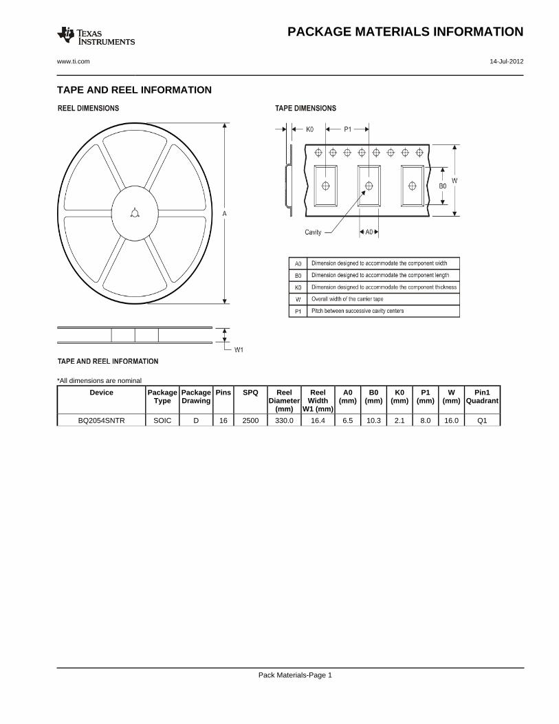
TAPE AND REEL INFORMATION
*All dimensions are nominal
Device PackageType
PackageDrawing
Pins SPQ ReelDiameter
(mm)
ReelWidth
W1 (mm)
A0(mm)
B0(mm)
K0(mm)
P1(mm)
W(mm)
Pin1Quadrant
BQ2054SNTR SOIC D 16 2500 330.0 16.4 6.5 10.3 2.1 8.0 16.0 Q1
PACKAGE MATERIALS INFORMATION
www.ti.com 14-Jul-2012
Pack Materials-Page 1
*All dimensions are nominal
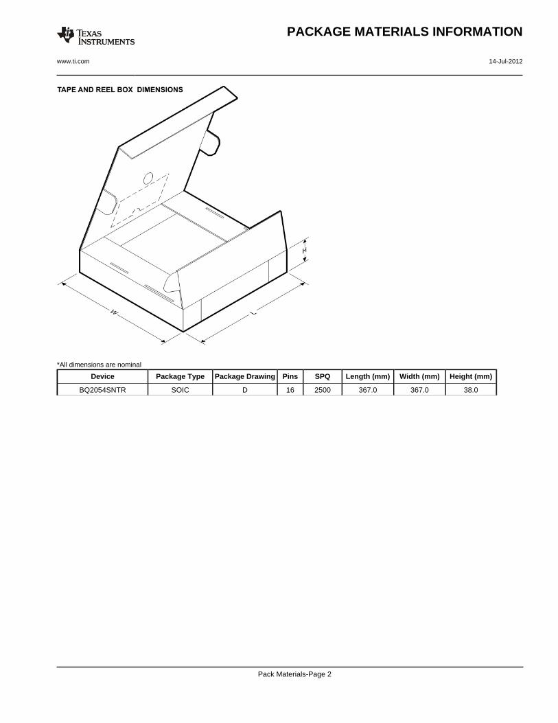
Device Package Type Package Drawing Pins SPQ Length (mm) Width (mm) Height (mm)
BQ2054SNTR SOIC D 16 2500 367.0 367.0 38.0
PACKAGE MATERIALS INFORMATION
www.ti.com 14-Jul-2012
Pack Materials-Page 2
IMPORTANT NOTICE
Texas Instruments Incorporated (TI) reserves the right to make corrections, enhancements, improvements and other changes to itssemiconductor products and services per JESD46, latest issue, and to discontinue any product or service per JESD48, latest issue. Buyersshould obtain the latest relevant information before placing orders and should verify that such information is current and complete.TI’s published terms of sale for semiconductor products (http://www.ti.com/sc/docs/stdterms.htm) apply to the sale of packaged integratedcircuit products that TI has qualified and released to market. Additional terms may apply to the use or sale of other types of TI products andservices.Reproduction of significant portions of TI information in TI data sheets is permissible only if reproduction is without alteration and isaccompanied by all associated warranties, conditions, limitations, and notices. TI is not responsible or liable for such reproduceddocumentation. Information of third parties may be subject to additional restrictions. Resale of TI products or services with statementsdifferent from or beyond the parameters stated by TI for that product or service voids all express and any implied warranties for theassociated TI product or service and is an unfair and deceptive business practice. TI is not responsible or liable for any such statements.Buyers and others who are developing systems that incorporate TI products (collectively, “Designers”) understand and agree that Designersremain responsible for using their independent analysis, evaluation and judgment in designing their applications and that Designers havefull and exclusive responsibility to assure the safety of Designers' applications and compliance of their applications (and of all TI productsused in or for Designers’ applications) with all applicable regulations, laws and other applicable requirements. Designer represents that, withrespect to their applications, Designer has all the necessary expertise to create and implement safeguards that (1) anticipate dangerousconsequences of failures, (2) monitor failures and their consequences, and (3) lessen the likelihood of failures that might cause harm andtake appropriate actions. Designer agrees that prior to using or distributing any applications that include TI products, Designer willthoroughly test such applications and the functionality of such TI products as used in such applications.TI’s provision of technical, application or other design advice, quality characterization, reliability data or other services or information,including, but not limited to, reference designs and materials relating to evaluation modules, (collectively, “TI Resources”) are intended toassist designers who are developing applications that incorporate TI products; by downloading, accessing or using TI Resources in anyway, Designer (individually or, if Designer is acting on behalf of a company, Designer’s company) agrees to use any particular TI Resourcesolely for this purpose and subject to the terms of this Notice.TI’s provision of TI Resources does not expand or otherwise alter TI’s applicable published warranties or warranty disclaimers for TIproducts, and no additional obligations or liabilities arise from TI providing such TI Resources. TI reserves the right to make corrections,enhancements, improvements and other changes to its TI Resources. TI has not conducted any testing other than that specificallydescribed in the published documentation for a particular TI Resource.Designer is authorized to use, copy and modify any individual TI Resource only in connection with the development of applications thatinclude the TI product(s) identified in such TI Resource. NO OTHER LICENSE, EXPRESS OR IMPLIED, BY ESTOPPEL OR OTHERWISETO ANY OTHER TI INTELLECTUAL PROPERTY RIGHT, AND NO LICENSE TO ANY TECHNOLOGY OR INTELLECTUAL PROPERTYRIGHT OF TI OR ANY THIRD PARTY IS GRANTED HEREIN, including but not limited to any patent right, copyright, mask work right, orother intellectual property right relating to any combination, machine, or process in which TI products or services are used. Informationregarding or referencing third-party products or services does not constitute a license to use such products or services, or a warranty orendorsement thereof. Use of TI Resources may require a license from a third party under the patents or other intellectual property of thethird party, or a license from TI under the patents or other intellectual property of TI.TI RESOURCES ARE PROVIDED “AS IS” AND WITH ALL FAULTS. TI DISCLAIMS ALL OTHER WARRANTIES ORREPRESENTATIONS, EXPRESS OR IMPLIED, REGARDING RESOURCES OR USE THEREOF, INCLUDING BUT NOT LIMITED TOACCURACY OR COMPLETENESS, TITLE, ANY EPIDEMIC FAILURE WARRANTY AND ANY IMPLIED WARRANTIES OFMERCHANTABILITY, FITNESS FOR A PARTICULAR PURPOSE, AND NON-INFRINGEMENT OF ANY THIRD PARTY INTELLECTUALPROPERTY RIGHTS. TI SHALL NOT BE LIABLE FOR AND SHALL NOT DEFEND OR INDEMNIFY DESIGNER AGAINST ANY CLAIM,INCLUDING BUT NOT LIMITED TO ANY INFRINGEMENT CLAIM THAT RELATES TO OR IS BASED ON ANY COMBINATION OFPRODUCTS EVEN IF DESCRIBED IN TI RESOURCES OR OTHERWISE. IN NO EVENT SHALL TI BE LIABLE FOR ANY ACTUAL,DIRECT, SPECIAL, COLLATERAL, INDIRECT, PUNITIVE, INCIDENTAL, CONSEQUENTIAL OR EXEMPLARY DAMAGES INCONNECTION WITH OR ARISING OUT OF TI RESOURCES OR USE THEREOF, AND REGARDLESS OF WHETHER TI HAS BEENADVISED OF THE POSSIBILITY OF SUCH DAMAGES.Unless TI has explicitly designated an individual product as meeting the requirements of a particular industry standard (e.g., ISO/TS 16949and ISO 26262), TI is not responsible for any failure to meet such industry standard requirements.Where TI specifically promotes products as facilitating functional safety or as compliant with industry functional safety standards, suchproducts are intended to help enable customers to design and create their own applications that meet applicable functional safety standardsand requirements. Using products in an application does not by itself establish any safety features in the application. Designers mustensure compliance with safety-related requirements and standards applicable to their applications. Designer may not use any TI products inlife-critical medical equipment unless authorized officers of the parties have executed a special contract specifically governing such use.Life-critical medical equipment is medical equipment where failure of such equipment would cause serious bodily injury or death (e.g., lifesupport, pacemakers, defibrillators, heart pumps, neurostimulators, and implantables). Such equipment includes, without limitation, allmedical devices identified by the U.S. Food and Drug Administration as Class III devices and equivalent classifications outside the U.S.TI may expressly designate certain products as completing a particular qualification (e.g., Q100, Military Grade, or Enhanced Product).Designers agree that it has the necessary expertise to select the product with the appropriate qualification designation for their applicationsand that proper product selection is at Designers’ own risk. Designers are solely responsible for compliance with all legal and regulatoryrequirements in connection with such selection.Designer will fully indemnify TI and its representatives against any damages, costs, losses, and/or liabilities arising out of Designer’s non-compliance with the terms and provisions of this Notice.
Mailing Address: Texas Instruments, Post Office Box 655303, Dallas, Texas 75265Copyright © 2018, Texas Instruments Incorporated