Literature Research Report for Lift-Off...
28
1 Literature Research Report for Lift-Off Method done by Na Zhang for BME 390A, term project STRUCTURE OF THIS REPORT Background Required Conditions For Deposited Film That Can Be Lifted-Off The Key Elements For Good Lift-Off Method Different Ways to Perform The Lift-Off Process 1. Single Layer Resist Processing 1.1 Standard Photoresist Processing 1.2 Single Layer of Negative Photoresist 1.3 Very Thick Negative Photoresist Single Layer 1.4 Advantage and Disadvantage 2. Bi-Layer Resist Processing 2.1 PR/LOL 2000 2.1.1 Property of the LOL-2000 Lift-Off Layer 2.1.2 General Procedure 2.1.3 Predicted Possible Problems 2.1.4 Specific Procedure 2.1.5 Advantage 2.2 PR/ LOR Lift-Off Resist (or PMGI Resist) 2.2.1 Property of the LOR Lift-Off Resist and PMGI Resist 2.2.2 General Procedure 2.2.3 Specific Procedure 2.2.4 Advantage 2.3 PMMA/PMMA 2.3.1 Property of PMMA 2.3.2 Specific Procedure 2.4 PMMA/LOL2000 2.5 Composite Layers of Aluminum (Al) and Photoresist 2.5.1 Process 2.5.2 Notes 3. Tri-Layer Processing 4. Surface Modifies Resist Processing 5. Others
Transcript of Literature Research Report for Lift-Off...

1
Literature Research Report for Lift-Off Method
done by Na Zhang
for BME 390A, term project
STRUCTURE OF THIS REPORT
Background Required Conditions For Deposited Film That Can Be Lifted-Off The Key Elements For Good Lift-Off Method Different Ways to Perform The Lift-Off Process
1. Single Layer Resist Processing 1.1 Standard Photoresist Processing 1.2 Single Layer of Negative Photoresist 1.3 Very Thick Negative Photoresist Single Layer 1.4 Advantage and Disadvantage
2. Bi-Layer Resist Processing 2.1 PR/LOL 2000
2.1.1 Property of the LOL-2000 Lift-Off Layer 2.1.2 General Procedure
2.1.3 Predicted Possible Problems 2.1.4 Specific Procedure 2.1.5 Advantage
2.2 PR/ LOR Lift-Off Resist (or PMGI Resist) 2.2.1 Property of the LOR Lift-Off Resist and PMGI Resist 2.2.2 General Procedure 2.2.3 Specific Procedure 2.2.4 Advantage
2.3 PMMA/PMMA 2.3.1 Property of PMMA 2.3.2 Specific Procedure 2.4 PMMA/LOL2000 2.5 Composite Layers of Aluminum (Al) and Photoresist
2.5.1 Process 2.5.2 Notes
3. Tri-Layer Processing 4. Surface Modifies Resist Processing 5. Others

2
Comparison Between Positive and Negative Photoresists Attachment Reference
Liftoff Processes
Background: [1, 19]
"Lift-off" is a simple, easy method for making metallic patterns on a substrate, especially for those noble metal thin films such as platinum, tantalum, nickel or iron which are difficult to be etched by conventional methods. The general Lift-off process is: First a pattern is defined on a substrate using photoresist. A film, usually metallic, is deposited all over the substrate, covering the photoresist and areas in which the photoresist has been cleared. During the actual lifting-off, the photoresist under the film is removed with solvent, taking the film with it, and leaving only the film which was deposited directly on the substrate.
Required conditions for the deposited film that can be lifted-off: [19]
1. During film deposition, temperatures cannot be high enough to burn the photoresist.
2. Adhesion of the deposited film on the substrate is very good. 3. The film can be easily wetted by the solvent. 4. The film is thin enough and/or grainy enough to allow solvent to seep
underneath. 5. The film is not elastic and is thin and/or brittle enough to tear along adhesion
lines. 6. The film quality is not absolutely critical. Photoresist will outgas very slightly
in vacuum systems, which may adversely affect the quality of the deposited film.
The Key Elements for Good Lift-off Result: create an undercut profile, this way the mask has an etched wall with a
negative slope Prebake temperature is the parameter with the greatest influence on undercut
rate. The other influential parameters also include prebake time, exposure dose of the imaging resist, choice of developer, develop mode and develop time.

3
Careful consideration should be given to the resist/developer system
Different ways to perform the lift-off process:
Note: Which method to choose will depend on the process requirements.
1. Single Layer Resist Processing 1.5 Standard Photoresist Processing 1.6 Single Layer of Negative Photoresist 1.7 Very Thick Negative Photoresist Single Layer 1.8 Advantage and Disadvantage
2. Bi-Layer Resist Processing 2.1 PR/LOL 2000
2.1.1 Property of the LOL-2000 Lift-Off Layer 2.1.2 General Procedure
2.1.3 Predicted Possible Problems 2.1.4 Specific Procedure 2.1.5 Advantage
2.2 PR/ LOR Lift-Off Resist (or PMGI Resist) 2.2.1 Property of the LOR Lift-Off Resist and PMGI Resist 2.2.2 General Procedure 2.2.3 Specific Procedure 2.2.4 Advantage
2.3 PMMA/PMMA 2.3.1 Property of PMMA 2.3.2 Specific Procedure 2.4 PMMA/LOL2000 2.5 Composite Layers of Aluminum (Al) and Photoresist
2.5.1 Process 2.5.2 Notes
3. Tri-Layer Processing 4. Surface Modifies Resist Processing 5. Others
1. Single layer resist processing
1.1 Standard photoresist processing [19]
4
Only one mask step and the standard photolithography procedure is involved. The main disadvantage of this method is that the film is deposited on the sidewall of the photoresist, and adheres to the substrate even after the resist removal. This sidewall may be peeled off in subsequent processing, resulting in particulates and shorts, or it may flop over and interfere with etches or depositions that follow.
Post-develop bake is recommended before film deposition based on the condition that bake time and temperature are well controlled.
Lift-off can be accomplished by immersing in acetone. The length of time for lift-off will depend on the film quality (generally, the higher the film quality, the more impermeable it is and the longer it will take to lift-off.) The sidewalls from deposited film can be removed using a gentle swipe of a clean-room swab or a directed stream of acetone from a squeeze bottle. Keep the substrate immersed in acetone until all the film has been lifted-off and there are no traces of film particulates -- once particles dry on the substrate, they are difficult to remove.
a.) Substrate with AZ3612 resist.
b.) Following expose and develop.
c.) Following film deposition.
d.) Following lift-off.
e.) Following mechanical "scrub".
1.2 Negative photoresist NR7-3000 PY [1,9,10]
Procedure:
spin-coat NR7-3000 PY @3000 rpm for 40 seconds heat treatment on hot plate @ 130oC for 60 s UV light with wavelength of 366 nm, intensity 6mW/cm2 for 30s bake on hot plate at 100oC for 60 s

5
develop in RD6 for 40 s
Note:
NR7-3000 PY can be easily washed off by acetone or resist remover RR2 NR7-3000 PY cam be exposed to ~200oC without cracking thickness <= 2µm
1.3 Very thick negative photoresist (SU-8) [1, 9, 10]
Procedure:
dehydrate the silicon substrate in an oven @ 110oC for >30 min spin-coat SU-8 @950 rpm for 20 seconds bake on hot plate @ 93oC for 18 min UV light with intensity 10 mW/cm2 for 120 s bake on hot plate at 95oC for 8 min develop in XPSU-8 for 3 min
Note:
Used for certain MEMS devices such as microactuator based on shape memory alloys where the transduction material may have a thickness >=5 µm
No chemical solution can effectively dissolve the cross linked SU-8 plasma etching with O2/C2F6 flow ratio of 100/25 can etch the SU-8 resist with an
etch rate of ~ 1.2 µm/min SU-8 cam be exposed to ~200oC without crack thickness >=5 µm
1.4 Advantage and Disadvantage:
Advantage: Easy to handle, fewer process steps Disadvantage: Low resolution, sidewall effect, ragged window edge
2. Bi-layer resist processing [22]
Two layers materials are required for this process. A thin film of the assisting material is first deposited. A layer of resist is spined over this layer and patterned through photolithography. This
6
way the assisting material layer is exposed. (figure 5a). This layer is then wet etched so as to undercut the resist (figure 5b). The metal is then deposited on the wafer, typically by a process known as evaporation (figure 5c). The resist is removed taking away the unwanted metal with it (figure 5d). The assisting layer is then stripped off too, leaving the metal pattern alone (figure 5e).
figure 5.
In the assisted lift off, an intermediate layer assists in the process to ensure a clean lift off and well defined metal pattern. When noble metals are used it is desirable to deposit a thin layer of a more active metal (eg, chrome/ Titanium) first, to ensure good adhesion of the noble metal. The key for bi-layer technology is that the bottom layer has higher sensitivity to the exposure dose, or has a higher dissolution rate in the developer
2.1 PR/LOL 2000 [2, 19, 23, 24]
2.1.1 Property of the LOL-2000 Lift-Off Layer [23]:
The LOL-2000 Lift-Off Layer a material is a non-photosensitive material which dissolves in photoresist developer in a controlled way. It is placed under the normal photoresist. After the photoresist is fully developed and the dissolution of the photoresist stops, the developer continues to dissolve the LOL-2000 layer in the open areas and further in under the resist edge, producing the clearence necessary for liftoff. Dissolution rate is dependent on baking temperature and time. (see following figures)
7
2.1.2 General Procedure [19]
a.) Substrate with underlying LOL2000 layer (purple) and overlying layer of common photoresist (e.g., AZ3612 )(brown.)
b.) Area of common photoresist exposed to UV (light purple).
c.) Develop in standard developer. The developer will etch the underlying LOL2000.
d.) Directional sputter film deposition.
e.) Lift-off and clean.
2.1.3 Predicted possible problems: [2, 23, 24]
• Overdevelopment may lose parts of the pattern . • Too long development may cause the too deep undercut and resist
will sag down, and the clearance gap between the substrate and the top resist will disappear.
• The LOL-2000 does not dissolve well in acetone. If doing liftoff in acetone, a final cleanup step need to be done in photoresist developer, NMP (remover 1165) or oxygen plasma afterwards.
• The LOL-2000 thickness is upward limited to about 200nm@2000rpm spin speed, and this puts a limit to the deposited film thickness to the same order. Coat several layers of LOL-2000 may be a possibility.
• Do NOT postbake. It will destroy the liftoff profile. • Choose developer carefully. Use MF319 instead of MF322,
because MF322 is too strong and the liftoff layer dissolves too fast.

8
• If less undercut is desired, a higher LOL baking temperature (130 - 180 degrees C) should be used.
2.1.4 Specific procedures: See Specific Process----PR/LOL 2000 DUAL LAYER RESIST PROCESSING in the attachment (Page 16)
2.1.5 Advantage: Reliable undercut sufficient to ensure good lift-off with thin film edge quality without flakes or fences; Good resolution
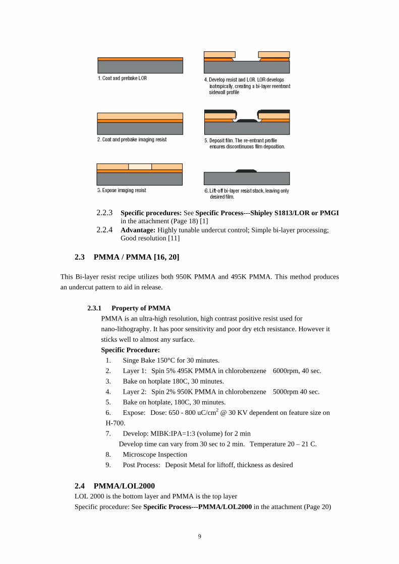
2.2 PR/ LOR Lift-Off Resist (or PMGI Resist) [1, 11 ]
2.2.1 Property of the LOR Lift-Off Resist and PMGI Resist [11]
PMGI is appropriate for many multilayer applications such as lift-off processing and T-gate fabrication. It is a positive tone resist with special material and performance properties. PMGI resists will not intermix when used in combination with imaging resists. In addition the dissolution properties can be very carefully controlled, which makes them well suited for critical level lift-off processes where precise undercut control is required.
MICROCHEM'S line of LOR lift-off resists comprises PMGI (polymethylglutarimide) resists specially suited for etch-sensitive applications. LOR products are available for a wide range of thicknesses when used with conventional positive resists together. This kind of resists produces easily-controlled reentrant profiles, ideal for sputtered and evaporative additive processes.
TYPES OF LOR RESISTS
LOR A series designed to work with metal-ion-free developers, relatively low dissolution rates, ideally suited for thin-film processes
LOR B series designed to work with metal-ion-bearing developers, relatively high dissolution rates, ideally suited for thick-film processes
Each series has several resists designed for a range of thicknesses
2.2.2 General Procedure [11]
9
2.2.3 Specific procedures: See Specific Process---Shipley S1813/LOR or PMGI
in the attachment (Page 18) [1] 2.2.4 Advantage: Highly tunable undercut control; Simple bi-layer processing;
Good resolution [11]
2.3 PMMA / PMMA [16, 20]
This Bi-layer resist recipe utilizes both 950K PMMA and 495K PMMA. This method produces an undercut pattern to aid in release.
2.3.1 Property of PMMA
PMMA is an ultra-high resolution, high contrast positive resist used for nano-lithography. It has poor sensitivity and poor dry etch resistance. However it sticks well to almost any surface. Specific Procedure:
1. Singe Bake 150°C for 30 minutes. 2. Layer 1: Spin 5% 495K PMMA in chlorobenzene 6000rpm, 40 sec. 3. Bake on hotplate 180C, 30 minutes. 4. Layer 2: Spin 2% 950K PMMA in chlorobenzene 5000rpm 40 sec. 5. Bake on hotplate, 180C, 30 minutes. 6. Expose: Dose: 650 - 800 uC/cm2 @ 30 KV dependent on feature size on H-700. 7. Develop: MIBK:IPA=1:3 (volume) for 2 min
Develop time can vary from 30 sec to 2 min. Temperature 20 – 21 C. 8. Microscope Inspection 9. Post Process: Deposit Metal for liftoff, thickness as desired
2.4 PMMA/LOL2000 LOL 2000 is the bottom layer and PMMA is the top layer Specific procedure: See Specific Process---PMMA/LOL2000 in the attachment (Page 20)

10
2.5 Aluminum/Photoresist [1]
2.5.1 Process:
1. A thick layer of Al (the thickness of Al should be greater than that of the thin film device material) was first deposited followed by a spin-coat of photoresist (e.g., AZ 1811, ~1 �m).
2. The mask pattern was defined into the photoresist layer. By using the patterned photoresist as the etch mask, the Al layer was wet chemically etched. In order to create an overhang structure with the photoresist, the Al layer was intentionally over-etched, Fig. 3a.
3. The device material, was then deposited, Fig. 3b.
4. A lift-off was done by dissolving the photoresist in acetone followed by etching
the Al sacrificial layer with phosphoric acid, Fig. 3c.
2.5.2 Notes: The phosphoric acid used to etch Al is highly selective to Al and does not attack Ta/Pt/Au metal. The thickness of the sacrificial Al be thicker than that of the metal interconnect. appropriate thickness of the sacrificial Al was ~750 nm, and the Al etch time was 3
minutes in phosphoric acid with mild agitation materials that are attacked by Al etch solution cannot be used as the device materials
The resultant metal interconnects and the SEM pictures of the fabricated mask using the tri-level resist scheme.
3. Lift-off mask fabricated by using a tri-level / four-level resist method[1,3,4] The processes are illustrated as following:
11
Step 1. (Fig 1a) A thin layer of aluminum is deposited onto a substrate. This layer is used as a sacrificial layer to solve the micromasking problem resulting from the reactive ion etching of the photoresist. [2in] Later, a thick layer of photoresist is spin coated upon the aluminum layer. After the application, the photoresist is baked which hardens the film, completely eliminates its photosensitivity and renders it opaque at the exposure wavelength. Deposite a thin intermediate masking layer on the top of thick photoresist, followed by spin coating a thin layer of photoresist.
Layers (from bottom to top)
Thickness Way to Put Notes
aluminum 100 nm deposite Photoresist (e.g., AZ 1818)
1.5-2µm Spin coat Bake after application (140oC, 30 minutes)
Intermediate layer (e.g.,tungsten)
100 nm deposite
Thin photoresist (e.g., AZ 1818)
0.3-0.5µm Spin coat
Table 1
Step 2. (Fig 1b) Through photolithography method, a device pattern is defined into the thin photoresist layer (AZ1811), and transferred into the underlying composite layer by two consecutive reactive ion etching of W and photoresist, and one wet chemical etching of Al. Etch condition are illustrated in table 2. Patterned wafer is then formed.
Layer to be patterned Pattern way Pressure (m Torr) Etch time (minute) Thin photoresist Photolithography method W Ion etch (etch gas: CF4) 14 4 Thick photoresist Ion etch (Oxygen) 15 30 Al Wet chemical etch Table 2
12
Step 3. (Fig 1c )
The thin film materials, e.g., Ta/Pt/Au are then deposited onto the patterned wafer. (fig.1c) Step 4. (Fig. 1d)
Place the wafer into appropriate solution (e.g. acetone) with or without ultrasonic agitation. The underlying photoresist is dissolved carrying away the metals deposited on the top, while the metals which were deposited directly onto the substrate stayed intact. The Al sacrificial layer was then etched off by phosphoric acid. The tri-level method provides good resolution and linewidth control for the mask. But because of the vertical sidewalls of the mask, the thin layer of device materials (e.g., Ta/Pt/Au) may also be deposited on the wall during the metal deposition. So untrasonic agitation may be used during the photoresist dissovling process to break the thin metal layer at the edge of the mask opening. Results:
Advantage: Good line width resolution Disadvantage: Complex process and longer processing time
The resultant metal interconnects and the SEM pictures of the fabricated mask using the tri-level resist scheme.
4. Surface modifies resist processing [2, 5, 6, 7, 8, 14, 19]
By soaking in chlorobenzene or toluene, the top surface of the photoresist can be chemically modified to develop at a slower rate than the underlying resist. The standard photoresist procedure or bi-layer photoresists procedure is used, and the wafer is soaked in chlorobenzene (for 10 minutes, typically) or toluene (for 1 minute, usually) either prior to UV-expose or just after, but prior to develop. And the wafer is blown dry and baked briefly. This way, the solubility of the top-most

13
layer of the resist in the developer is reduced, producing an overhang structure in the resist mask and create an undercut profile after standard development. However, both of the chemicals are kind of harmful to the environment, and need to pay attention to.
Specific Procedure: see Specific Process ------Surface modifies resist processing in the attachment (page 22)
Advantage and Disadvantage:
Advantage: simple method, can be used to assist bi-layer process Disadvantage: Difficult to control the proper soak time Lift-off processed using toluene or chlorobenzene are highly irreproducible Chlorobenzene is toxic and Toluene is also a dangerous chemical.
5. Other procedures
See Specific Process---Other Procedure in the attachment (Page 26)
Comparison of The Results Method Resolution Processing
Time Process Steps
Film thickness
Comments
Single Layer
Low Lowest Lowest Not good for
thin film
N/A
Bi-Layer High middle middle Any N/A
Tri-Layer High most most Any N/A
Surface Modify
High middle middle Any Combined
with double
layer method
Overall, the Bi-layer method is the best.
Comparison Between Positive and Negative Photoresists [26]

14
Negative resist lift-off process has fewer steps than the positive resist lift-off, and is
therefore more cost- and time-effective. Negative photoresist will produce ragged metal edge, the results coming from positive
photoresist is good. Negative resists were popular in the early history of integrated circuit processing, but
positive resist gradually became more widely used since they offer better process controllability for small geometry features.
15
Attachment
16
Specific Process----PR/LOL 2000 DUAL LAYER RESIST PROCESSING
a) AZ3612 / LOL2000 DUAL LAYER RESIST PROCESSING [19]
• Use dedicated LOL2000 boats. Do not use standard Litho cassettes to handle LOL2000 coated wafers because this LOL2000 will contaminate the cassettes and it cannot be removed with Acetone.
• Singe for 30 minutes at 150°C . • Prime with HMDS before LOL2000 (not absolutely necessary, but results are
consistently better.) • Apply LOL2000 on the Headway ONLY at 3000 rpm's for 60 seconds (=2000Å). • Bake for 5 minutes on a 150°C or 170°C hotplate, or 30 minutes oven bake. • Coat with photoresist, the SVG coater may be used. AZ3612 will work fine. If the devices
have topography, use at least 1.6 microns of photoresist to ensure coverage. • Bake for 60 seconds on a 90°C hotplate. • Expose with standard exposure times for the photoresist used. • Develop for 60 seconds in LDD26W, may use the SVG developer track. • Bake 60 seconds on a 110°C hotplate • Lift-off can be done using either:
o Acetone. However, Acetone alone does not completely remove LOL2000 polymer. Additional clean should be done using O2 plasma ash, or photoresist developer, or Microposit Remover 1165.
o Ultrasonic immersion in Microposit Remover 1165 at 50°C. Carefully monitor the temperature, as the flash point of Microposit 1165 is around 85°C. If PRS1000 or SVC127 resist strippers are used to do the final clean, make sure the substrate is completely dry before immersing in these solutions (trace moisture will result in highly corrosive conditions, which may etch the metal.)
b) S-1813 example process [2]
• Clean substrate • Spin spacer layer LOL-2000 @ 3000 rpm for 200nm thickness • Bake 140 C on hot plate for 5 minutes • Spin resist layer S-1813 @ 4000 rpm for 1.3 um thickness • Bake 110 C on hot plate for 2 minutes • Expose through pattern mask,
o 45s @ 2.45 mW/cm2 (110 mJ/cm^2 nominally)at UV250 mask aligner, intensity measured using the 400nm probe.
17
o 15 s @ 10 mW/cm2 (150 mJ/cm^2 nominally)at UV400 mask aligner, intensity measured using the 400nm probe.
• Develop in MF319 for 30 sec, CAREFUL agitation • Rinse in DI water • Blow dry CAREFULLY. • Ash at 50W 250mTorr Oxygen for 30 s • Deposit thin film • Lift off in acetone or NMP (Remover 1165)
o If do liftoff in acetone, do a final clean step in photoresist developer , NMP stripper, or oxygern plasma afterwards. LOL-2000 does not dissolve well in acetone.
• Rinse in IPA and blow dry.
(Notes: The conditions above should be seen only as a guideline, modifications of exposure and development time
will be necessary for each application dependent on substrate reflectivity, etc. There may also be differences when
exposing using the UV250 or the UV400 mask aligner as they have different spectrums in the 365 - 436 nm range.)
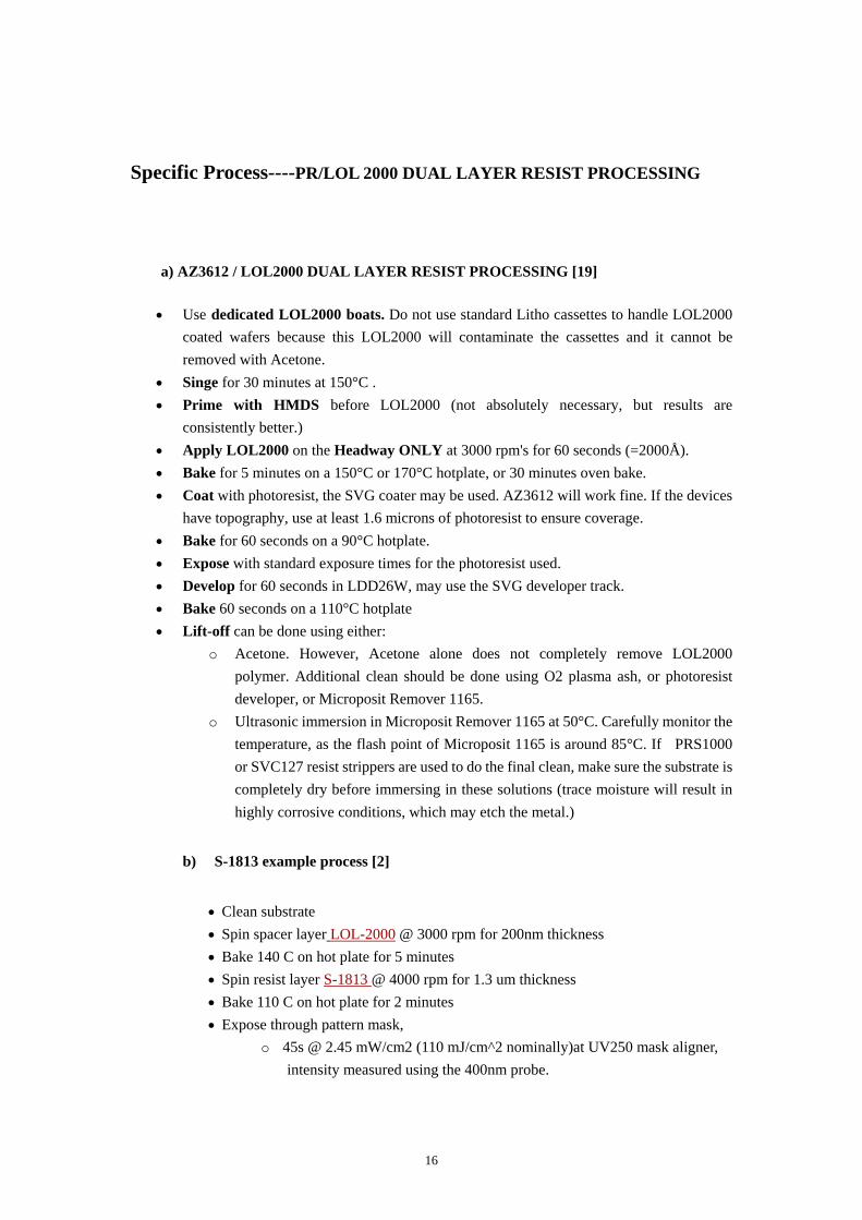
Resist patterns created at SnL using LOL-2000 and UV5 resist

18
Specific process----PR/LOR or PMGI
Method #1 Shipley S1813/LOR-3A [13,11,15]
1. Pre-clean substrate using RF-O2 plasma or UV-ozone at 170C (5 min) if the substrates are contaminated with organics. Remove adhered water molecules from the substrate using a 200C hotplate bake (5 min). 2. Spin LOR-3A at 500 rpm (2 seconds) followed by 3000 rpm (35 seconds) 3. Bake on hotplate at 170C for 5 minutes 4. Spin on Shipley S1813 photoresist at 500 rpm (2 seconds) followed by 5000 rpm (35 seconds) 5. Bake at 115C for 120 seconds 6. Expose in Karl Suss maskaligner for 8 seconds, or when using the AB-M maskaligner, for 3 seconds. 7. Develop in CD-26 for 45 seconds. Rinse in DI water and spin or blow dry 8. Hotplate bake at 125C for 5 minutes 9. Undercut etch in CD-26 for 1 minute, rinse in DI-H2O and spin or blow dry. 10. Evaporate metal up to 300 nm thick 11. Lift off the LOR and photoresist using microchem’s “remover PG” at 70C for 10 minutes using a magnetic spinner. Notes to the steps: 1. The Samco UV ozone machine effectively removes ultrathin organic contamination and old photoresist residue without mechanically and electronically damaging the substrate surface. If damage is acceptable though just use the RF-O2 plasma cleaner. 2. LOR-3A also works as an adhesion promoter. It’s glass temperature is 190C, which is much higher than that of photoresist, so substrate heating during evaporation is not a problem as with photoresist where the resist can harden and impossible to remove. 3. No need to prebake for 10 minutes at 90 or 100C, this is a mistake. Make sure during spinning that no resist goes to the backside of the substrate, because this will prevent good thermal contact with the hotplate and poor development. Make sure the hotplate is clean also, especially for small samples. 4. Exposure time is very critical with CD-26 developer. This is the parameter to accurately vary to obtain nice results. Underexposure leads to resist residue, overexposure to ragged resist edges. 5. the 125C bake is necessary to create a larger difference in etch rate. Without this step, poorly exposed S1813 etches the same rate or faster than the LOR, preventing formation of an undercut. 6. The undercut etch rate is about 400 nm/min for our process. 7. Do not use acetone; LOR does not dissolve in it. Remover PG is an NMP (Nmethylpyrrolidone) based solvent. Do not go higher than 80C. (88C is the flashpoint of NMP). Sonication can also be used, if the adhesion of the metal film is sufficient (Nickel, Titanium, Chromium should be ok, if evaporated below 5e-7 mbar during evaporation). Be careful sonicators are not meant for

19
flammable liquids because the liquid can heat up by the shaking and could potentially eventually start burning. Room temperature lift off using the remover PG also works. The necessary temperature depends a bit on the heating of the LOR during evaporation. If the substrate got hot (>190C), use 70C for remover PG, if it didn’t get warm at all, you may try remover PG at room temperature. Method #2 PR/PMGI or LOR 10A [1] 1. spin coat @ 3000 rpm for 30 s 2. heat treatment on a hot plate @ 112oC for 140 s 3. spin coat another layer of photoresist (AZ 1811) @ 4000 rpm for 30 s 4. bake in an oven @ 90 oC for 30 min 5. expose to UV light with 10 mW/cm2, wavelength of 405 nm for 7 s 6. develop in LDD 26W for 210 s with mild agitation 7. deposite thin film materials 8. dissolve the photoresist in acetone with ultrasonic agitation for 10 min Notes:
Each photoresist will have a thickness of ~1µm The faster etch rate of the underlying photoresist, LOR 10A , resulted in an
overhang structure

20
Specific Process---PMMA / LOL2000 [25] Step 1: Preparation of stamps 1 inch silicon wafer with 300 nm thick thermally grown oxide Step 2: Preparation of two layers Layers thickness notes LOL(lift-off layer) 2000 (bottom)
20-60 nm Soft-baked in convection oven at 180oC for 30 minutes after application
PMMA (top)
100 nm baked in convection oven at 180oC for 30 minutes
Step 3: Nanoimprinting The stamp is in contact with PMMA which works well with their anti-sticking protection. Parameters: Temperature: 180-200oC Pressure: 50 bar Imprint time: 3-10 min.
Layers Way to imprint NOTES PMMA e-beam
lithograpy(EBL)+UV lithogragphy
Oxygen ashing at 5
mbar for 15-30 s to
remove residual
PMMA after
imprinting (note 1)
LOL(lift-off layer) 2000
Developer MF319 (Shipley)
MF319 open up
windows to the
substrate and create
the undercut profile
in the resist (note 2)
Note: 1.The resigual layer of PMMA covers the LOL and thus prohibits the possibility of creating an undercut.

21
2. MF319 is mixed with deionized water to give a dissolution time of around 1 min. for a 50 nm thick layer. Slowing
down the process will enhance control of the undercut and prevent over development.
Step 4: Deposite metal film by thermal evaporation Step 5: Two step Lift-off process 1. warm acetone bath which breaks apart the metal layer and dissolves the PMMA 2. warm Remover S-1165 bath which removes the LOL and remaining metal note: Use of ultra sonic agitation is redundant Results: 1. Good pattern transfer down to 20 nm
2. Linewidth: 50nm-400nm
3. dots with 15nm in diameter (with conical SiO2 pillars)
22
Specific Process ------Surface modifies resist processing
a) Standard Lift-off Process i) Method #1 Chlorobenzene Process [8,14]
(1) HMDS - 3 minutes (2) Spin on Shipley 1400-31, 6000 rpm, 30 seconds (3) Prebake in oven at 70oC - 20 minutes (4) Chlorobenzene rinse - 10 minutes (5) Blow dry (6) Expose (3.9-4.2 min in Canon; ~ 6 sec in Kasper) (7) Develop in Microposit concentrate - 45 seconds. Do not overdevelop or lines will collapse. ii) Method # 2
Using Shipley S-1813 positive resist with Toluene [2,5,6,7]
Photoresist Shipley S-1813 (positive) used together with Toluene as a surface modifier to produce an undercut edge profile to ensure good liftoff. This is similar to the well-known Chlorobenzene process, but it is using a non-chlorinated solvent so save the environment, following the EU 'substitution-rule' to phase out the usage of chlorinated substances whenever possible.
• Clean substrate • Spin resist S-1813 @ 4000 rpm • Soft bake, 90 C on hot plate for 1 min
Steps in order to remove thick resist on edges of wafer
• Expose through edge removal mask, 10 mW/cm^2 for 30 sec • Develop in MF322 for 20 sec
23
• Rinse in DI water
Steps for pattern exposure
• Expose through pattern mask, 10 mW/cm^2 for 8 sec • Soak in Toluene for 1 min • Blow dry and drybake, 90C on hotplate for 15 s • Develop in MF322 for 20-30 sec • Rinse in DI water • Blow dry. • Ash at 50W 250mTorr Oxygen for 30 s
Comments:
Produces a nice undercut profile if the exposure is sharp, i.e if the mask-resist gap is small. To maintain the good edge profile, be careful not to ash too strongly, and do NOT postbake. The process above is used on YBCO with a gold cap layer. Exposure time may have to be modified in accordance with the reflectivity of your substrate material.
Toluene is a non-chlorinated solvent, which is better for the environment, but it is still a dangerous chemical, possibly carcinogenic. Be careful.
b) bi-layer Liftoff Process i) method #1 [8]
1. Coat wafer with Shipley 1400-31 photoresist: 6000rpm for 30 secs. 2. Bake PR in 90oC oven (top shelf) for 15 minutes. 3. Remove wafer from oven and let cool. 4. Coat wafer with PR as in step 1. 5. Bake wafer on 80oC hotplate for 5 minutes. 6. Remove wafer from hotplate and let cool. 7. Submerge wafer in chlorobenzene for 10 mins. 8. Remove wafer from chlorobenzene and blow dry with N2 gun. Do
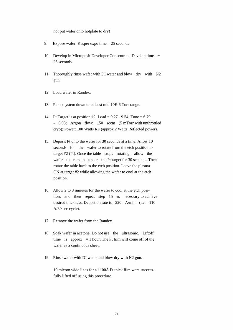
24
not put wafer onto hotplate to dry! 9. Expose wafer: Kasper expo time = 25 seconds 10. Develop in Microposit Developer Concentrate: Develop time ~ 25 seconds. 11. Thoroughly rinse wafer with DI water and blow dry with N2 gun. 12. Load wafer in Randex. 13. Pump system down to at least mid 10E-6 Torr range. 14. Pt Target is at position #2: Load = 9.27 - 9.54; Tune = 6.79 - 6.98; Argon flow: 150 sccm (5 mTorr with unthrottled cryo); Power: 100 Watts RF (approx 2 Watts Reflected power). 15. Deposit Pt onto the wafer for 30 seconds at a time. Allow 10 seconds for the wafer to rotate from the etch position to target #2 (Pt). Once the table stops rotating, allow the wafer to remain under the Pt target for 30 seconds. Then rotate the table back to the etch position. Leave the plasma ON at target #2 while allowing the wafer to cool at the etch position. 16. Allow 2 to 3 minutes for the wafer to cool at the etch posi- tion, and then repeat step 15 as necessary to achieve desired thickness. Depostion rate is 220 A/min (i.e. 110 A/30 sec cycle). 17. Remove the wafer from the Randex. 18. Soak wafer in acetone. Do not use the ultrasonic. Liftoff time is approx = 1 hour. The Pt film will come off of the wafer as a continuous sheet. 19. Rinse wafer with DI water and blow dry with N2 gun. 10 micron wide lines for a 1100A Pt thick film were success- fully lifted off using this procedure.
25
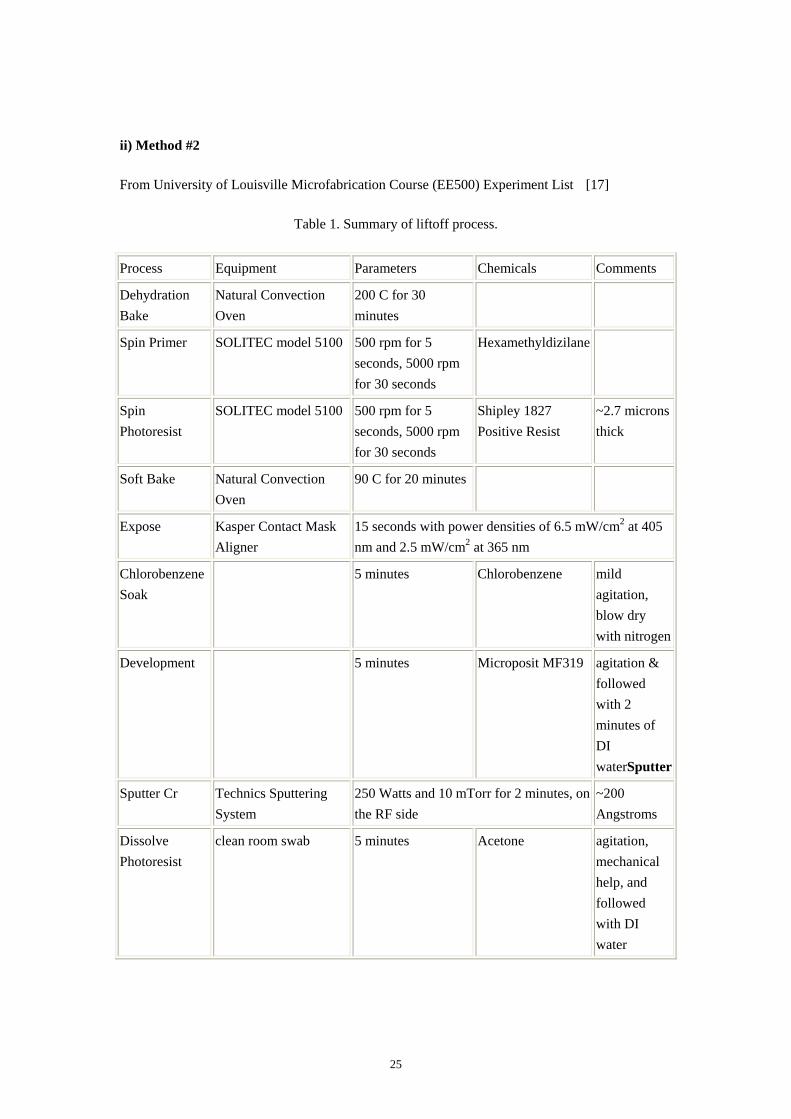
ii) Method #2
From University of Louisville Microfabrication Course (EE500) Experiment List [17]
Table 1. Summary of liftoff process.
Process Equipment Parameters Chemicals Comments
Dehydration Bake
Natural Convection Oven
200 C for 30 minutes
Spin Primer SOLITEC model 5100 500 rpm for 5 seconds, 5000 rpm for 30 seconds
Hexamethyldizilane
Spin Photoresist
SOLITEC model 5100 500 rpm for 5 seconds, 5000 rpm for 30 seconds
Shipley 1827 Positive Resist
~2.7 microns thick
Soft Bake Natural Convection Oven
90 C for 20 minutes
Expose Kasper Contact Mask Aligner
15 seconds with power densities of 6.5 mW/cm2 at 405 nm and 2.5 mW/cm2 at 365 nm
Chlorobenzene Soak
5 minutes Chlorobenzene mild agitation, blow dry with nitrogen
Development 5 minutes Microposit MF319 agitation & followed with 2 minutes of DI waterSputter
Sputter Cr Technics Sputtering System
250 Watts and 10 mTorr for 2 minutes, on the RF side
~200 Angstroms
Dissolve Photoresist
clean room swab 5 minutes Acetone agitation, mechanical help, and followed with DI water
26
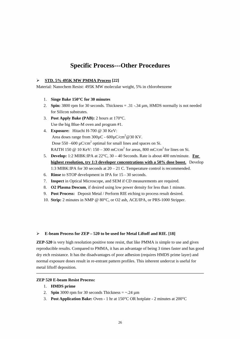
Specific Process---Other Procedures
STD. 5% 495K MW PMMA Process [22] Material: Nanochem Resist: 495K MW molecular weight, 5% in chlorobenzene
1. Singe Bake 150°C for 30 minutes 2. Spin: 3800 rpm for 30 seconds. Thickness = .31 -.34 µm, HMDS normally is not needed
for Silicon substrates. 3. Post Apply Bake (PAB): 2 hours at 170°C.
Use the big Blue-M oven and program #1. 4. Exposure: Hitachi H-700 @ 30 KeV:
Area doses range from 300µC - 600µC/cm2@30 KV. Dose 550 –600 µC/cm2 optimal for small lines and spaces on Si. RAITH 150 @ 10 KeV: 150 – 300 mC/cm2 for areas, 800 mC/cm2 for lines on Si.
5. Develop: 1:2 MIBK:IPA at 22°C, 30 – 40 Seconds. Rate is about 400 nm/minute. For highest resolution, try 1:3 developer concentrations with a 50% dose boost. Develop 1:3 MIBK:IPA for 30 seconds at 20 – 21 C. Temperature control is recommended.
6. Rinse to STOP development in IPA for 15 - 30 seconds. 7. Inspect in Optical Microscope, and SEM if CD measurements are required. 8. O2 Plasma Descum, if desired using low power density for less than 1 minute. 9. Post Process: Deposit Metal / Perform RIE etching to process result desired. 10. Strip: 2 minutes in NMP @ 80°C, or O2 ash, ACE/IPA, or PRS-1000 Stripper.
E-beam Process for ZEP – 520 to be used for Metal Liftoff and RIE. [18]
ZEP-520 is very high resolution positive tone resist, that like PMMA is simple to use and gives reproducible results. Compared to PMMA, it has an advantage of being 3 times faster and has good dry etch resistance. It has the disadvantages of poor adhesion (requires HMDS prime layer) and normal exposure doses result in re-entrant pattern profiles. This inherent undercut is useful for metal liftoff deposition.
ZEP 520 E-beam Resist Process:
1. HMDS prime 2. Spin 3000 rpm for 30 seconds Thickness = ~.24 µm 3. Post Application Bake: Oven - 1 hr at 150°C OR hotplate - 2 minutes at 200°C
27
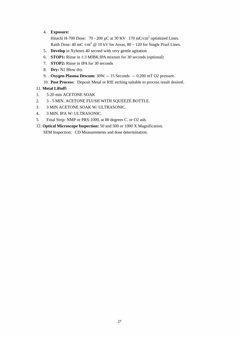
4. Exposure: Hitachi H-700 Dose: 70 - 200 µC at 30 KV 170 mC/cm2 optimized Lines. Raith Dose: 40 mC /cm2 @ 10 kV for Areas, 80 – 120 for Single Pixel Lines.
5. Develop in Xylenes 40 second with very gentle agitation 6. STOP1: Rinse in 1:3 MIBK:IPA mixture for 30 seconds (optional) 7. STOP2: Rinse in IPA for 30 seconds 8. Dry: N2 Blow dry. 9. Oxygen Plasma Descum: 30W. -- 15 Seconds -- 0.200 mT O2 pressure. 10. Post Process: Deposit Metal or RIE etching suitable to process result desired.
11. Metal Liftoff: 1. 5-20 min ACETONE SOAK 2. 3 - 5 MIN. ACETONE FLUSH WITH SQUEEZE BOTTLE. 3. 3 MIN ACETONE SOAK W/ ULTRASONIC. 4. 3 MIN. IPA W/ ULTRASONIC. 5. Final Strip: NMP or PRS-1000, at 80 degrees C. or O2 ash. 12. Optical Microscope Inspection: 50 and 500 or 1000 X Magnification. SEM Inspection: CD Measurements and dose determination.

28
Reference
[1]. Shih-Chia Chang and Jeffrey M. Kempisty, 'Lift-off Methods for MEMS Devices ', Mat. Res. Soc. Symp. Proc. Vol. 729
[2]. Swedish Nanometer Lab, http://fy.chalmers.se/assp/snl/ [3]. J. M. Moran and D. Maydan, 'High Resolution, Steep Profile Resist Patterns,' J. Vac. Sci.
Technol., 16(60), p.1620, (1979). [4]. J. H. Bruning, 'Optical Imaging for Microfabrication,' J. Vac. Sci. Technol. 23(2), p.1147,
(1980). [5]. 'Modified soaking solvent for single resist lift-off structures, ' Hamel-CJ, Weed-DR,
IBM-Technical-Disclosure-Bulletin. vol.21, no.8, Jan. 1979, 3103 [6]. Single-step optical lift-off process, Hatzakis-M, Canavello-BJ, Shaw-JM,
IBM-Journal-of-Research-and-Development. vol.24, no.4, July 1980, 452-60 [7]. Thin film process for Nb/NbO/sub x//(Pb-In-Au) Josephson junction devices, Salmi-J,
Knuutila-J, Seppa-H, Immonen-P, Thin-Solid-Films. vol.126, no.1-2, 12 April 1985, 77-81 [8]. Berkeley Microlab website: http://microlab.berkeley.edu [9]. B. Loechel and A. Maciossek, ”Surface Micro Components Fabricated by UV Depth
Lithography and Electroplating”, Proceedings, SPIE Conference on Micromachining and Microfabrication Process Technology, p. 174, (1995).
[10]. K. Y. LEE, et al., “Micromachining Application of High Resolution Ultrathick Photoresist,” J. Vac. Technol., B 13(6), p. 3012, (1995)
[11]. 'LOR Lift-Off Resists' from www.MICROCHEM.com [12]. NANO™PMGI Resists from www.MICROCHEM.com [13]. 'A reliable lift-off process', By Douwe Monsma and Ian Applebaum Aug 2002, Marcuslab,
Harvard University [14]. http://www.nnf.cornell.edu/1998reu/ra/Bishop.pdf [15]. http://www.samcointl.com/prod/UV-1/index.html [16]. NANO™PMMA and Copolymer from www.MICROCHEM.com [17]. http://mitghmr.spd.louisville.edu/course/exp77.html [18]. http://snf.stanford.edu/Process/Lithography/EBResist/ZEP520Liftoff.html [19]. http://snf.stanford.edu/Process/Lithography/liftoff.html [20]. http://snf.stanford.edu/Process/Lithography/EBResist/JKProcess1.html [21]. http://www.dbanks.demon.co.uk/ueng/liftoff.html [22]. http://snf.stanford.edu/Process/Lithography/EBResist/STD495KPMMA.html [23]. http://fy.chalmers.se/assp/snl/public/resists/LOL2000.html [24]. http://fy.chalmers.se/assp/snl/public/wproc/LOL2000_Liftoff.html [25]. P. Carlberg , M Graczyk, E.-L. Sarwe, I. Maximov, M. Beck, L. Montelius,'Lift-off process for nanoimprint lithography', Microelectronic Engineering 67–68 (2003) 203–207 [26]. http://www.nsec.harvard.edu/AP298/Chen.pdf