Linear Regulator as a Dynamic Voltage Scaling Power … Description 1 System Description The...
18
LP3878-ADJ TPL0401A 0 ± 7 N VOUT VIN Host processor (SoCs, processors DSPs, FPGAs) Power rail 3.6 V to 5.5 V VBIAS ADJ I 2 C VCORE VCORE 1.2 V to 1.6 V TI Designs Linear Regulator as a Dynamic Voltage Scaling Power Supply TI Designs Design Features TI Designs provide the foundation that you need • Output Voltage Ranges from 1.2 V to 1.6 V With 90 including methodology, testing, and design files to Steps in Between quickly evaluate and customize the system. TI Designs • Output Voltage Adjustable Through I 2 C Interface help you accelerate your time to market. • Up to 800-mA Output Current Design Resources • Output Voltage Enable and Disable Featured Applications Tool Folder Containing Design Files TIDA-00531 LP3878-ADJ Product Folder • PDAs TPL0401A Product Folder • Wearables • MP3 Players ASK Our E2E Experts • Battery Operated Devices WEBENCH® Calculator Tools An IMPORTANT NOTICE at the end of this TI reference design addresses authorized use, intellectual property matters and other important disclaimers and information. All trademarks are the property of their respective owners. 1 TIDU950 – April 2015 Linear Regulator as a Dynamic Voltage Scaling Power Supply Submit Documentation Feedback Copyright © 2015, Texas Instruments Incorporated
Transcript of Linear Regulator as a Dynamic Voltage Scaling Power … Description 1 System Description The...

LP3878-ADJ
TPL0401A0 �± 7 N��
VOUTVIN
Host processor (SoCs, processors DSPs, FPGAs)xxPower rail
3.6 V to 5.5 V
VBIAS ADJ
I2C
VCORE
VCORE 1.2 V to 1.6 V
TI DesignsLinear Regulator as a Dynamic Voltage Scaling PowerSupply
TI Designs Design FeaturesTI Designs provide the foundation that you need • Output Voltage Ranges from 1.2 V to 1.6 V With 90including methodology, testing, and design files to Steps in Betweenquickly evaluate and customize the system. TI Designs • Output Voltage Adjustable Through I2C Interfacehelp you accelerate your time to market.
• Up to 800-mA Output CurrentDesign Resources • Output Voltage Enable and Disable
Featured ApplicationsTool Folder Containing Design FilesTIDA-00531LP3878-ADJ Product Folder • PDAsTPL0401A Product Folder • Wearables
• MP3 PlayersASK Our E2E Experts • Battery Operated DevicesWEBENCH® Calculator Tools
An IMPORTANT NOTICE at the end of this TI reference design addresses authorized use, intellectual property matters and otherimportant disclaimers and information.
All trademarks are the property of their respective owners.
1TIDU950–April 2015 Linear Regulator as a Dynamic Voltage Scaling Power SupplySubmit Documentation Feedback
Copyright © 2015, Texas Instruments Incorporated
System Description www.ti.com
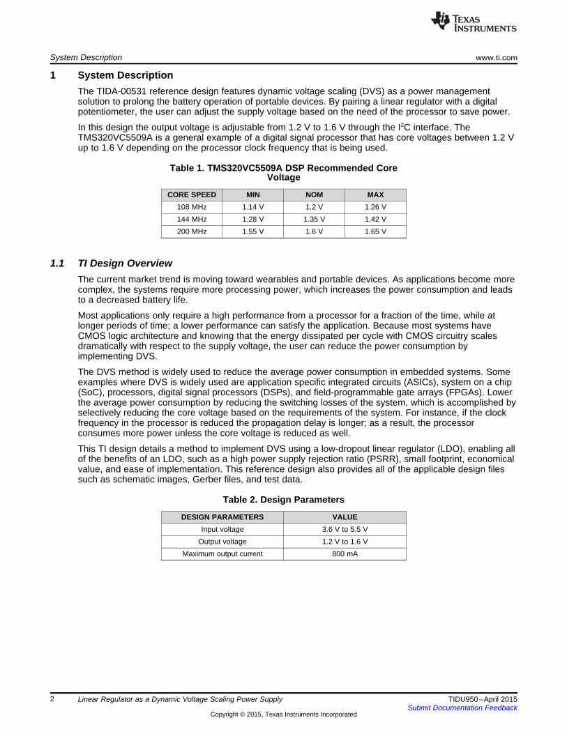
1 System DescriptionThe TIDA-00531 reference design features dynamic voltage scaling (DVS) as a power managementsolution to prolong the battery operation of portable devices. By pairing a linear regulator with a digitalpotentiometer, the user can adjust the supply voltage based on the need of the processor to save power.
In this design the output voltage is adjustable from 1.2 V to 1.6 V through the I2C interface. TheTMS320VC5509A is a general example of a digital signal processor that has core voltages between 1.2 Vup to 1.6 V depending on the processor clock frequency that is being used.
Table 1. TMS320VC5509A DSP Recommended CoreVoltage
CORE SPEED MIN NOM MAX108 MHz 1.14 V 1.2 V 1.26 V144 MHz 1.28 V 1.35 V 1.42 V200 MHz 1.55 V 1.6 V 1.65 V
1.1 TI Design OverviewThe current market trend is moving toward wearables and portable devices. As applications become morecomplex, the systems require more processing power, which increases the power consumption and leadsto a decreased battery life.
Most applications only require a high performance from a processor for a fraction of the time, while atlonger periods of time; a lower performance can satisfy the application. Because most systems haveCMOS logic architecture and knowing that the energy dissipated per cycle with CMOS circuitry scalesdramatically with respect to the supply voltage, the user can reduce the power consumption byimplementing DVS.
The DVS method is widely used to reduce the average power consumption in embedded systems. Someexamples where DVS is widely used are application specific integrated circuits (ASICs), system on a chip(SoC), processors, digital signal processors (DSPs), and field-programmable gate arrays (FPGAs). Lowerthe average power consumption by reducing the switching losses of the system, which is accomplished byselectively reducing the core voltage based on the requirements of the system. For instance, if the clockfrequency in the processor is reduced the propagation delay is longer; as a result, the processorconsumes more power unless the core voltage is reduced as well.
This TI design details a method to implement DVS using a low-dropout linear regulator (LDO), enabling allof the benefits of an LDO, such as a high power supply rejection ratio (PSRR), small footprint, economicalvalue, and ease of implementation. This reference design also provides all of the applicable design filessuch as schematic images, Gerber files, and test data.
Table 2. Design Parameters
DESIGN PARAMETERS VALUEInput voltage 3.6 V to 5.5 V
Output voltage 1.2 V to 1.6 VMaximum output current 800 mA
2 Linear Regulator as a Dynamic Voltage Scaling Power Supply TIDU950–April 2015Submit Documentation Feedback
Copyright © 2015, Texas Instruments Incorporated
LP3878-ADJ
TPL0401A0 �± 7 N��
VOUTVIN
Host processor (SoCs, processors DSPs, FPGAs)xxPower rail
3.6 V to 5.5 V
VBIAS ADJ
I2C
VCORE
VCORE 1.2 V to 1.6 V
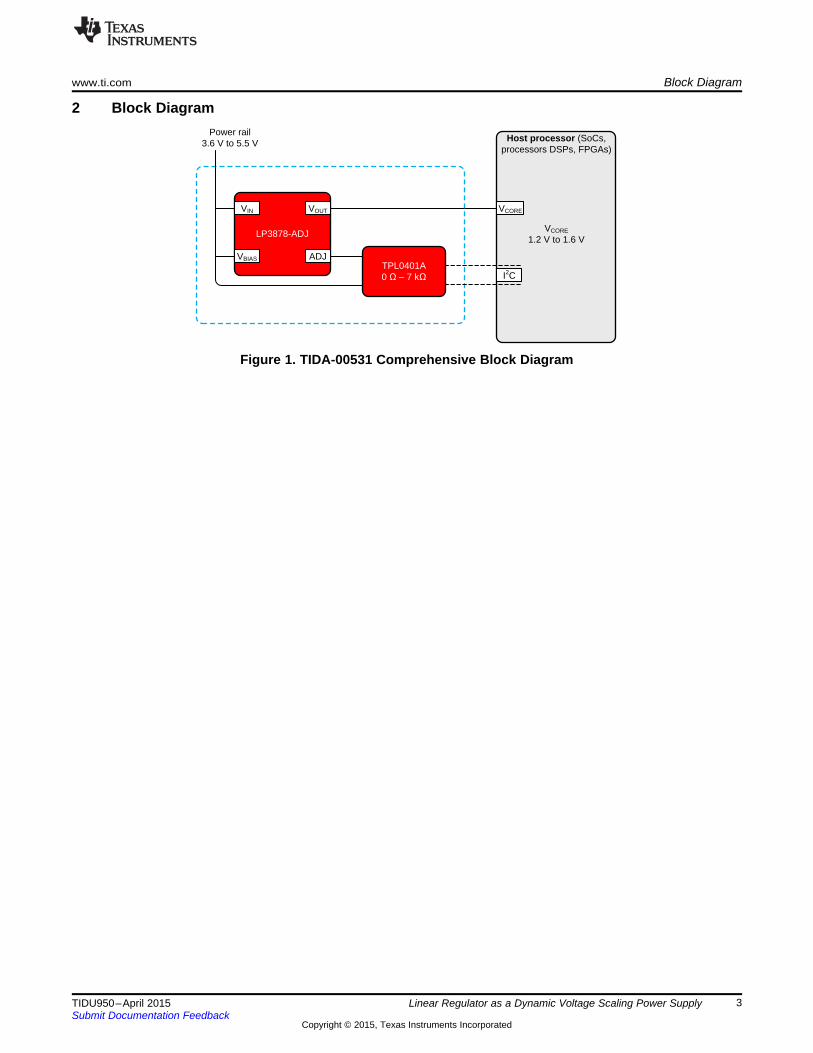
www.ti.com Block Diagram
2 Block Diagram
Figure 1. TIDA-00531 Comprehensive Block Diagram
3TIDU950–April 2015 Linear Regulator as a Dynamic Voltage Scaling Power SupplySubmit Documentation Feedback
Copyright © 2015, Texas Instruments Incorporated
+-
2
7
8
5416
3
1 VVREF
Error
Amp
LP3878- ADJ
BYPASS
N/C
GROUND
INADJ OUT
N/C
SHUTDOWN+
Component Selection www.ti.com
3 Component SelectionThe TIDA-00531 design guide features the following devices:
LDO: The LP3878-ADJ is a micropower, 800-mA low-noise, “ceramic stable” adjustable voltage regulator.For further details regarding the LP3878-ADJ device, see Section 3.1.
Consider the following parameters when selecting the LDO:• Adjustable output by resistor divider• Maximum constant output current 800 mA• Low IQ at shutdown
The alternative parts must have an adjustable pin:• LP38851 has similar functionality at lower output voltages (0.8 V)• LP38853 has similar functionality at a higher output current (3 A)
Digital potentiometer: The TPL0401A-10 is a 128 TAPS digital potentiometer with an I2C interface in asmall SC-70 package. For further details regarding the TPL0401A-10 device, see Section 3.2.
Consider the following parameters when selecting the digital potentiometer:• Standard I2C interface• Typical end-to-end resistance of 10 kΩ• 128 wiper positions
The following lists alternative parts with similar functionality:• TPL0401B-10 featuring a different I2C Interface• TPL0501-100 uses a serial peripheral interface (SPI) interface• TPL0102-100 uses non-volatile memory
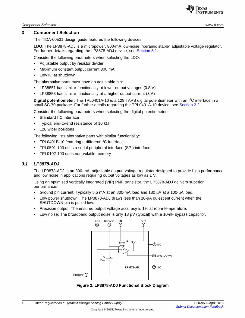
3.1 LP3878-ADJThe LP3878-ADJ is an 800-mA, adjustable output, voltage regulator designed to provide high performanceand low noise in applications requiring output voltages as low as 1 V.
Using an optimized vertically integrated (VIP) PNP transistor, the LP3878-ADJ delivers superiorperformance:• Ground pin current: Typically 5.5 mA at an 800-mA load and 180 µA at a 100-µA load.• Low power shutdown: The LP3878-ADJ draws less than 10-µA quiescent current when the
SHUTDOWN pin is pulled low.• Precision output: The ensured output voltage accuracy is 1% at room temperature.• Low noise: The broadband output noise is only 18 µV (typical) with a 10-nF bypass capacitor.
Figure 2. LP3878-ADJ Functional Block Diagram
4 Linear Regulator as a Dynamic Voltage Scaling Power Supply TIDU950–April 2015Submit Documentation Feedback
Copyright © 2015, Texas Instruments Incorporated
WIPER
REGISTERI C INTERFACE2
SCL
SDA
VDD
GND
H
W
TP0L401A
www.ti.com Component Selection
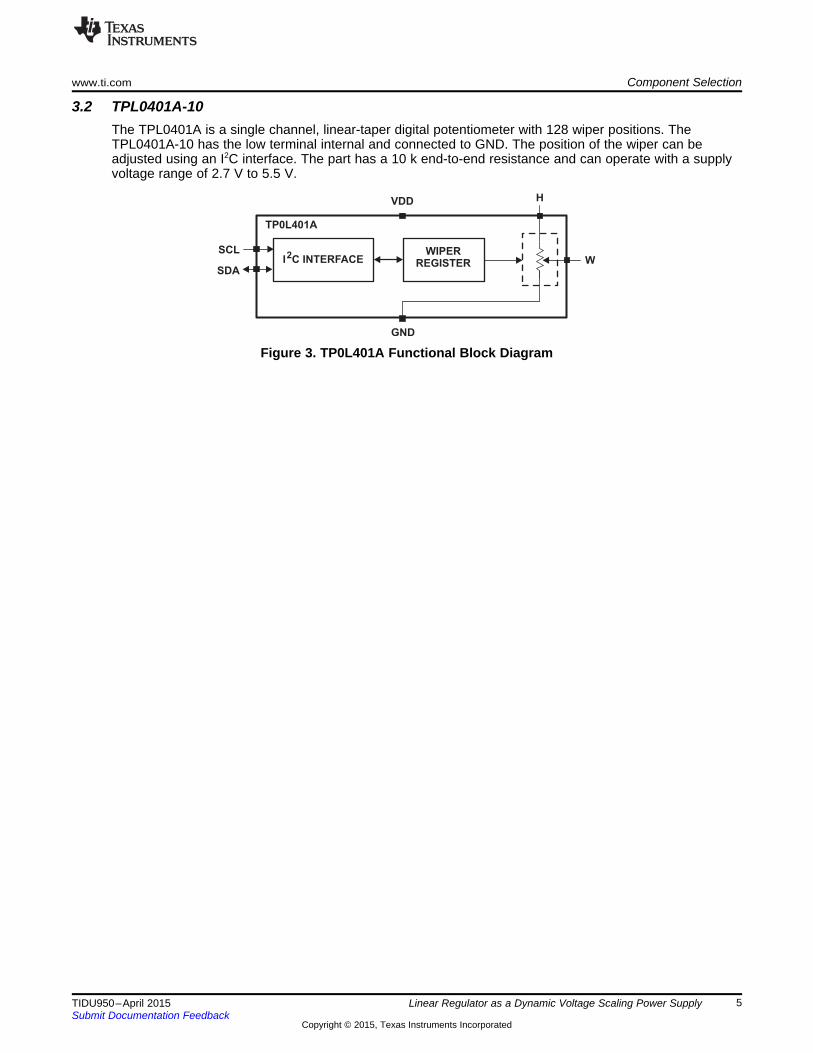
3.2 TPL0401A-10The TPL0401A is a single channel, linear-taper digital potentiometer with 128 wiper positions. TheTPL0401A-10 has the low terminal internal and connected to GND. The position of the wiper can beadjusted using an I2C interface. The part has a 10 k end-to-end resistance and can operate with a supplyvoltage range of 2.7 V to 5.5 V.
Figure 3. TP0L401A Functional Block Diagram
5TIDU950–April 2015 Linear Regulator as a Dynamic Voltage Scaling Power SupplySubmit Documentation Feedback
Copyright © 2015, Texas Instruments Incorporated
FF
z
1 1C 0.005 F 5 nF
2 F R1 2 52 KHz 604= = = m =
p p ´ ´ p
p
FF
1F
R1 R22 C
R1 R2
=
´p ´
+
z
FF
1F
2 C R1=
p ´
IN OUT _MAXV V 2 V 1.6 V 2 V 3.6 V= + = + =
System Design and Component Selection www.ti.com
4 System Design and Component SelectionThe following system considerations apply only for the conditions of this design. Verifying the ratings andoperating conditions for the parts used in this design is essential. Find this information in the respectivedatasheets. If the parameters do not fit the application, consider one of the alternative parts from Section 3or perform an easy parametric search at http://www.ti.com/ldo.
4.1 Input Voltage ConsiderationThe input voltage of the LP3878-ADJ must be 2 V higher than the expected output voltage; in this case,the minimum input voltage must remain above 3.6 V for a stable output voltage of 1.6 V.
To eliminate high frequency noise and for stability, low equivalent series resistance (ESR) X7R ceramiccapacitors are placed as close as possible to the input and output pin.
(1)
The digital potentiometer TPL0401A-10 has an input voltage range from 2.7 V to 5.5 V. Because theD-potentiometer and the LDO share the same power rail, the input range of this system is from 3.6 V to5.5 V.
If using an independent power rail to power the D-potentiometer, then the input voltage supply of the LDOcan be as high as 16 V, allowing an input voltage range from 3.6 V to 16 V.
4.2 Capacitor Selection Consideration
4.2.1 Noise Bypass CapacitorA 10-nF bypass capacitor reduces noise on the regulator output and is required for loop stability. Thefollowing recommendation must be taken into account:• The bypass capacitor leakage must never exceed 100 nA.• High-quality ceramic capacitors with either an NP0 or C0G dielectric typically have very low leakage.• 10-nF polypropylene and polycarbonate film capacitors typically have an extremely low leakage
current.
4.2.2 Feedforward CapacitorThe feedforward capacitor CFF) is required to increase phase margin, ensure loop stability, and improvetransient response.
The CFF forms both a pole and zero in the loop gain. The zero provides a beneficial phase lead (whichincreases phase margin), and the pole adds an undesirable phase lag that must be minimized.
The zero frequency is determined by the values of CFF and R1:
(2)
The pole frequency is determined by the value of CFF and the parallel combination of R1 and R2:
(3)
For VOUT ≤ 2.5 V, CFF must be selected to set the zero frequency in the range of about 50 KHz to 200 KHz.
The following Equation 4 is used to calculate CFF. The zero frequency is set to 52 KHz.
(4)
6 Linear Regulator as a Dynamic Voltage Scaling Power Supply TIDU950–April 2015Submit Documentation Feedback
Copyright © 2015, Texas Instruments Incorporated

LP3878-ADJ
TPL0401AI2C
DPOT
R LS
RHW
RHW
H
L
WRTOT
RHEOSTAT MODE B
HW TOT
Decimal value of step codeR R 1
128
æ öæ ö= ´ -ç ÷ç ÷
è øè ø
OUT REF
R1V V (1 )
R2= +
www.ti.com System Design and Component Selection
4.2.3 Input and Output CapacitorsInput and output capacitors eliminate high frequency noise and are necessary for loop stability. Considerthe following recommendations:• Utilize X7R or X5R ceramic capacitors to minimize tolerance and variation with temperature• Capacitance ESR in the 50- to 200-KHz range must not exceed 25 mΩ• Input and output caps must be located less than 1 inch from the input and output pins• Input minimum capacitance of 4.7 µF• Output minimum capacitance of 10 µF• Minimum of ± 20% capacitance tolerance
4.3 Output Voltage ConfigurationThe output voltage on this LDO in a typical application is determined by an external resistor divider R1(upper-side resistor) and R2 (lower-side resistor).
(5)
The LP3878-ADJ datasheet specifies that VREF is typically 1 V at the adjustable pin.
In the TIDA-00531 reference design a digital potentiometer is placed across R2 with a series resistor. Byadjusting the resistance of the potentiometer through the I2C interface, the resistor divider ratio changesaccordingly, thus changing the output voltage.
4.3.1 Resistors Values SelectionTI recommends selecting resistor values of a high quality and tight tolerance. Figure 5 represents thecomponents that define the output voltage. To ensure loop stability the lower-side resistance (RLS) mustnot exceed 5 kΩ.
Figure 4 shows the implemented digital potentiometer configuration. The RHW is the adjustable resistancebetween R3 and ground. Calculate RHW using Equation 6:
(6)
Figure 4. TPL0401A Configuration Figure 5. Resistor Divider
The TPL0401A-10 datasheet specifies that its typical maximum resistance is 10 kΩ with a tolerance of±20%; meaning that the maximum value could be from 8 kΩ to 12 kΩ. To address these tolerances andmaintain the maximum output voltage to no higher than 1.6 V, use the digital potentiometer within a rangeof 0 Ω (RHW_MIN) to 7 kΩ (RHW_MAX). This range allows for 90 steps of resolution in a typical D-potentiometer.
To be compliant with the 5-kΩ rule, 3 kΩ was chosen for the RLS maximum value. Because 3 kΩ is thehighest value for the equivalent lower resistance, this setting yields the lowest expected voltage of 1.2 V.
7TIDU950–April 2015 Linear Regulator as a Dynamic Voltage Scaling Power SupplySubmit Documentation Feedback
Copyright © 2015, Texas Instruments Incorporated
( )( )
( )
( )POT _MAX LS _MAX
POT _MAX LS _MAX
D R2 R 7 k 1.2 k 3 kR2
7 k 1.2 k 3 kD R2 R
+ ´ W + W ´ W= =
W + W - W+ -
LS _MINMAX
R1 600R 1000
V 1 1.6 V 1
W= = = W
- -
OUTLS _MAX
REF
V 1.2 VR1 R 1 3 k 1 600
V 1 V
æ ö æ ö= ´ - = W ´ - = Wç ÷ ç ÷
è øè ø
System Design and Component Selection www.ti.com
Calculate R1 using Equation 7:
(7)
Calculate the minimum equivalent lower resistance RLS using Equation 8.
(8)
Resistor R3 is essential to avoid a short path to ground when the D-potentiometer is set to 0 Ω. A value of1.2 kΩ is selected for R3. Calculate the parallel resistance R2 using Equation 9.
(9)
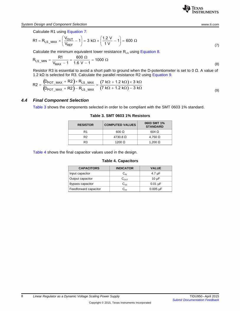
4.4 Final Component SelectionTable 3 shows the components selected in order to be compliant with the SMT 0603 1% standard.
Table 3. SMT 0603 1% Resistors
0603 SMT 1%RESISTOR COMPUTED VALUES STANDARDR1 600 Ω 604 ΩR2 4730.8 Ω 4,750 ΩR3 1200 Ω 1,200 Ω
Table 4 shows the final capacitor values used in the design.
Table 4. Capacitors
CAPACITORS INDICATOR VALUEInput capacitor CIN 4.7 μFOutput capacitor COUT 10 μFBypass capacitor CSS 0.01 µFFeedforward capacitor CFF 0.005 µF
8 Linear Regulator as a Dynamic Voltage Scaling Power Supply TIDU950–April 2015Submit Documentation Feedback
Copyright © 2015, Texas Instruments Incorporated
Start Address (01_1110) 0 Ack Command (00000000) Ack
Start Address (01_1110) 0 Ack Command (00000000) Ack
reStart Address (01_1110) 1 Ack Data Byte
I2C Write to A Register
I2C Read From A Register
Data Stop
noAck Stop
Ack
From Processor to DPOT
From toDPOT Processor
Data Outputby Transmitter
Data Outputby Receiver
SCL fromMaster
NACK
StartCondition
ACK
Clock Pulse forAcknowledgment
S
1 2 8 9
www.ti.com I2C Interface Details
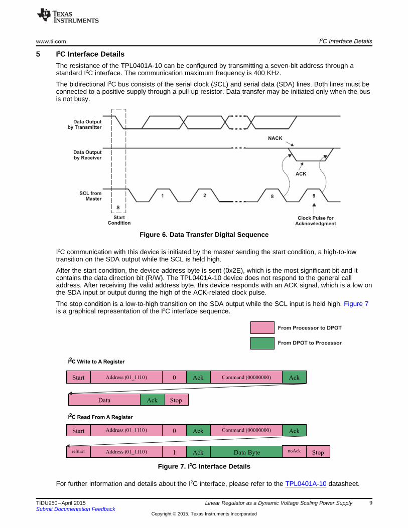
5 I2C Interface DetailsThe resistance of the TPL0401A-10 can be configured by transmitting a seven-bit address through astandard I2C interface. The communication maximum frequency is 400 KHz.
The bidirectional I2C bus consists of the serial clock (SCL) and serial data (SDA) lines. Both lines must beconnected to a positive supply through a pull-up resistor. Data transfer may be initiated only when the busis not busy.
Figure 6. Data Transfer Digital Sequence
I2C communication with this device is initiated by the master sending the start condition, a high-to-lowtransition on the SDA output while the SCL is held high.
After the start condition, the device address byte is sent (0x2E), which is the most significant bit and itcontains the data direction bit (R/W). The TPL0401A-10 device does not respond to the general calladdress. After receiving the valid address byte, this device responds with an ACK signal, which is a low onthe SDA input or output during the high of the ACK-related clock pulse.
The stop condition is a low-to-high transition on the SDA output while the SCL input is held high. Figure 7is a graphical representation of the I2C interface sequence.
Figure 7. I2C Interface Details
For further information and details about the I2C interface, please refer to the TPL0401A-10 datasheet.
9TIDU950–April 2015 Linear Regulator as a Dynamic Voltage Scaling Power SupplySubmit Documentation Feedback
Copyright © 2015, Texas Instruments Incorporated

CC OL _MAX RP
OL B
V V TR
I 0.8473 C
-
£ £
´
RP _MAX
B
TR
0.8473 C=
´
R 2 1 P BT T T 0.847298 R C= - = ´ ´
P B
t
R C
T CCV V 1 e
-´
æ öç ÷= ´ -ç ÷ç ÷è ø
CC OL _MAXP _MIN
OL
V VR
I
-
=
I2C Interface Details www.ti.com
5.1 Pull-Up ResistorsIf the master microcontroller (MCU) or CPU has open-collector SDA and SCL lines, they must beconnected to the supply voltage using pull-up resistors. Pulling the line up is necessary when the I2C linesare not driven low by the open-collector interface.
Selecting the correct resistor value is crucial because a small pull-up resistor can prevent the I2C linesfrom driving low enough to cross the logic low threshold. Conversely, a high resistor value may not allowthe signal to rise to the logic high threshold before the digital signal is pulled low again.
The minimum pull-up resistance is a function of supply voltage (VDD), max output low voltage (VOL), andsink current (IOL).
(10)
The maximum pull-up resistance is limited by the capacitance in bus CB, the bus capacitance isdetermined by the collective capacitance of all the pins and wire connections. The CB and pull-up resistorform a resistor-capacitor (RC) circuit, which increases the slew rate of the digital signal due to the RC timeconstant. The maximum resistance can be determined by calculating the rising time constant using theinput high voltage (VIH), input low voltage (VIL), and solving for the RP equation and bus capacitance.
The following Equation 11 is for the charging capacitor:
where• solving for VIH = VCC X 0.7 ≥ T1 = 1.203970 x RC• solving for VIL = VCC X 0.3 ≥ T2 = 0.3556675 x RC (11)
The rising time of the I2C bus can be written as:(12)
Solve for RP to find the maximum pull-up resistance, as Equation 13 shows.
(13)
Select a pull-up resistor in the middle of the range to provide as much guard bandwidth as possible.
(14)
For more detailed information and parameters about the I2C interface, please refer to the SLVA689application note.
10 Linear Regulator as a Dynamic Voltage Scaling Power Supply TIDU950–April 2015Submit Documentation Feedback
Copyright © 2015, Texas Instruments Incorporated
www.ti.com Layout Guidelines
6 Layout GuidelinesBe sure to use the proper printed circuit board (PCB) layout procedures to avoid instability caused byground loops and voltage drops. The input and output capacitors must be directly connected to the input,output, and ground pins of the regulator using traces which do not have other currents flowing throughout(Kelvin connect).
The best way to make this connection is to lay CIN and COUT near the device with short traces to the VIN,VOUT, and ground pins. The regulator ground pin must be connected to the external circuit ground so thatthe regulator and its capacitors have a single point to ground.
Note that some stability problems have been seen in applications where using vias to an internal groundplane at the ground points of the IC, input capacitors, and output capacitors. This instability is caused byvarying ground potentials at these nodes as a result of the current flowing through the ground plane. Usinga single-point ground technique for the regulator and the capacitors fixes the problem. Because a highcurrent flows through the traces going into VIN and coming from VOUT, TI recommends to use a four-terminal connection or “Kelvin connection” for the capacitor leads to these pins to prevent a voltage dropin series with the input and output capacitors.
11TIDU950–April 2015 Linear Regulator as a Dynamic Voltage Scaling Power SupplySubmit Documentation Feedback
Copyright © 2015, Texas Instruments Incorporated
GND
SD
SDA
SCL
3.6 V
Test Results www.ti.com
7 Test Results
7.1 Equipment UsedTable 5 is a list of the test equipment used in the previous sections.
Table 5. Test Equipment
TEST EQUIPMENT PART NUMBEROscilloscope Agilent MSO7034B
Voltage supply Agilent E61ANetwork analyzer Agilent E5061B
7.2 Default Output Voltage at Start-UpTable 6 shows the start-up default settings of the system. The default start-up resistance value ofTPL0401A-10 is typically at a mid-scale value (5 kΩ).
Table 6. Default Output Voltage Settings
HEX DPOT STEP RHW (Ω) RHW + R3 (RHW + R3) || R2 VOUT
0x3F 5080 Ω 6280 Ω 2704.4 Ω 1.23 V
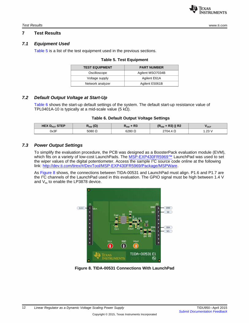
7.3 Power Output SettingsTo simplify the evaluation procedure, the PCB was designed as a BoosterPack evaluation module (EVM),which fits on a variety of low-cost LaunchPads. The MSP-EXP430FR5969™ LaunchPad was used to setthe wiper values of the digital potentiometer. Access the sample I2C source code online at the followinglink: http://dev.ti.com/tirex/#/DevTool/MSP-EXP430FR5969/Package/MSPWare.
As Figure 8 shows, the connections between TIDA-00531 and LaunchPad must align. P1.6 and P1.7 arethe I2C channels of the LaunchPad used in this evaluation. The GPIO signal must be high between 1.4 Vand VIN to enable the LP3878 device.
Figure 8. TIDA-00531 Connections With LaunchPad
12 Linear Regulator as a Dynamic Voltage Scaling Power Supply TIDU950–April 2015Submit Documentation Feedback
Copyright © 2015, Texas Instruments Incorporated
Frequency (Hz)
Rip
ply
Rej
ectio
n (d
B)
10 100 1000 10000 100000 1000000 1E+70
10
20
30
40
50
60
70
80
D004
Input Voltage (V)
Out
put V
olta
ge (
V)
2.5 3 3.5 4 4.5 5 5.51.1
1.2
1.3
www.ti.com Test Results
Table 7 shows the output voltage settings at the output voltage of interest in the TIDA-00531 referencedesign.
Table 7. Output Voltage Settings
HEX DPOT STEP RHW (Ω) RHW + R3 (RHW + R3) || R2 VOUT
0x7F 80 Ω 1280 Ω 1008 Ω 1.60 V0x6C 1560 Ω 2760 Ω 1745.7 Ω 1.35 V0x26 7030 Ω 8230 Ω 3011.7 Ω 1.20 V
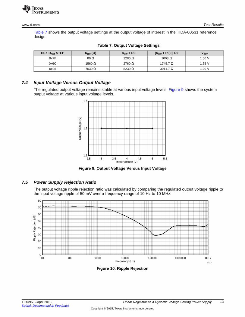
7.4 Input Voltage Versus Output VoltageThe regulated output voltage remains stable at various input voltage levels. Figure 9 shows the systemoutput voltage at various input voltage levels.
Figure 9. Output Voltage Versus Input Voltage
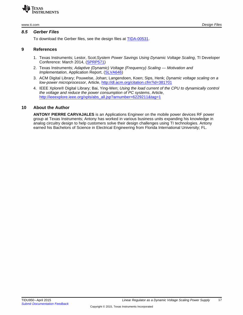
7.5 Power Supply Rejection RatioThe output voltage ripple rejection ratio was calculated by comparing the regulated output voltage ripple tothe input voltage ripple of 50 mV over a frequency range of 10 Hz to 10 MHz.
Figure 10. Ripple Rejection
13TIDU950–April 2015 Linear Regulator as a Dynamic Voltage Scaling Power SupplySubmit Documentation Feedback
Copyright © 2015, Texas Instruments Incorporated

Test Results www.ti.com
7.6 Start-Up and Shut Down TransitionThis test was done by removing or applying 3.6 V at the input voltage and measuring the transients at theoutput voltage pin. The voltage output was left in the default start-up state. The rising time from 0 V to1.23 V took approximately 16 µs. The falling time from 1.23 V to 0 V took an approximate 53 ms with a10-µF cap at the output pin to ground. Figure 11 and Figure 12 are scope shots of the output voltageduring start-up and shut down.
Figure 11. Start-Up Output Voltage Transient
Figure 12. Shut Down Output Voltage Transient
14 Linear Regulator as a Dynamic Voltage Scaling Power Supply TIDU950–April 2015Submit Documentation Feedback
Copyright © 2015, Texas Instruments Incorporated

Output Voltage (V)
RH
W (:
)
1.2 1.25 1.3 1.35 1.4 1.45 1.5 1.55 1.60
1000
2000
3000
4000
5000
6000
7000
www.ti.com Test Results
7.7 Voltage Steps ResolutionFigure 13 shows a graph of the computational results of the output voltage versus the RHW resistance ofthe digital potentiometer.
The user can expect to have a resolution of 90 steps with a typical digital potentiometer .
Figure 13. Digital Potentiometer Resistance Versus Output Voltage
15TIDU950–April 2015 Linear Regulator as a Dynamic Voltage Scaling Power SupplySubmit Documentation Feedback
Copyright © 2015, Texas Instruments Incorporated

Single point to ground for CIN and COUT to avoid
varying ground potentials
Short trace connecting pin 6 of U2 to R3
The CIN and COUT caps are placed close to the input and output
pins to minimize current loops
Solid ground plane to guarantee good
heat dissipation
IN4
ADJ6
GND3
NC7
SD8
DAP9
OUT5
BYP1
NC2
U1
LP3878MR-ADJ/NOPB
VDD1
GND2
SCL3
SDA4
W5
H6
U2
TPL0401A-10DCKR
4.7kR4
GND
GND
Vin
Vin
604R1
4.53kR2
1.40kR3
GND
0.1µFC1
Vin
10µFCout
GND
10µFCin
GND
510pFCff
Vin
Vin
SCL
SDA
0.01
µF
Css
GND
BYP
BYP
5
4
1
2
3
6
7
8
9
10
J2
SSW-110-23-F-S
5
4
1
2
3
6
7
8
9
10
J1
SSW-110-23-F-S
GND
GND
Vin
Vin
4.7kR5
GNDVout
GND
Vout
Vout
0
R6J1.8
J1.8
SCL
SDA
Design Files www.ti.com
8 Design Files
8.1 SchematicsTo download the schematics, see the design files at TIDA-00531.
Figure 14. TIDA-00531 Schematic
8.2 Bill of MaterialsTo download the bill of materials (BOM), see the design files at TIDA-00531.
8.3 Layout PrintsTo download the layout prints, see the design files at TIDA-00531.
8.4 Layout Guidelines
Figure 15. Layout Guidelines
16 Linear Regulator as a Dynamic Voltage Scaling Power Supply TIDU950–April 2015Submit Documentation Feedback
Copyright © 2015, Texas Instruments Incorporated
www.ti.com Design Files
8.5 Gerber FilesTo download the Gerber files, see the design files at TIDA-00531.
9 References
1. Texas Instruments; Lestor, Scot;System Power Savings Using Dynamic Voltage Scaling, TI DeveloperConference: March 2014, (SPRP571)
2. Texas Instruments; Adaptive (Dynamic) Voltage (Frequency) Scaling — Motivation andImplementation, Application Report, (SLVA646)
3. ACM Digital Library; Pouwelse, Johan; Langendoen, Koen; Sips, Henk; Dynamic voltage scaling on alow-power microprocessor, Article, http://dl.acm.org/citation.cfm?id=381701
4. IEEE Xplore® Digital Library; Bai, Ying-Wen; Using the load current of the CPU to dynamically controlthe voltage and reduce the power consumption of PC systems, Article,http://ieeexplore.ieee.org/xpls/abs_all.jsp?arnumber=6229211&tag=1
10 About the AuthorANTONY PIERRE CARVAJALES is an Applications Engineer on the mobile power devices RF powergroup at Texas Instruments; Antony has worked in various business units expanding his knowledge inanalog circuitry design to help customers solve their design challenges using TI technologies. Antonyearned his Bachelors of Science in Electrical Engineering from Florida International University; FL.
17TIDU950–April 2015 Linear Regulator as a Dynamic Voltage Scaling Power SupplySubmit Documentation Feedback
Copyright © 2015, Texas Instruments Incorporated
IMPORTANT NOTICE FOR TI REFERENCE DESIGNS
Texas Instruments Incorporated ("TI") reference designs are solely intended to assist designers (“Buyers”) who are developing systems thatincorporate TI semiconductor products (also referred to herein as “components”). Buyer understands and agrees that Buyer remainsresponsible for using its independent analysis, evaluation and judgment in designing Buyer’s systems and products.TI reference designs have been created using standard laboratory conditions and engineering practices. TI has not conducted anytesting other than that specifically described in the published documentation for a particular reference design. TI may makecorrections, enhancements, improvements and other changes to its reference designs.Buyers are authorized to use TI reference designs with the TI component(s) identified in each particular reference design and to modify thereference design in the development of their end products. HOWEVER, NO OTHER LICENSE, EXPRESS OR IMPLIED, BY ESTOPPELOR OTHERWISE TO ANY OTHER TI INTELLECTUAL PROPERTY RIGHT, AND NO LICENSE TO ANY THIRD PARTY TECHNOLOGYOR INTELLECTUAL PROPERTY RIGHT, IS GRANTED HEREIN, including but not limited to any patent right, copyright, mask work right,or other intellectual property right relating to any combination, machine, or process in which TI components or services are used.Information published by TI regarding third-party products or services does not constitute a license to use such products or services, or awarranty or endorsement thereof. Use of such information may require a license from a third party under the patents or other intellectualproperty of the third party, or a license from TI under the patents or other intellectual property of TI.TI REFERENCE DESIGNS ARE PROVIDED "AS IS". TI MAKES NO WARRANTIES OR REPRESENTATIONS WITH REGARD TO THEREFERENCE DESIGNS OR USE OF THE REFERENCE DESIGNS, EXPRESS, IMPLIED OR STATUTORY, INCLUDING ACCURACY ORCOMPLETENESS. TI DISCLAIMS ANY WARRANTY OF TITLE AND ANY IMPLIED WARRANTIES OF MERCHANTABILITY, FITNESSFOR A PARTICULAR PURPOSE, QUIET ENJOYMENT, QUIET POSSESSION, AND NON-INFRINGEMENT OF ANY THIRD PARTYINTELLECTUAL PROPERTY RIGHTS WITH REGARD TO TI REFERENCE DESIGNS OR USE THEREOF. TI SHALL NOT BE LIABLEFOR AND SHALL NOT DEFEND OR INDEMNIFY BUYERS AGAINST ANY THIRD PARTY INFRINGEMENT CLAIM THAT RELATES TOOR IS BASED ON A COMBINATION OF COMPONENTS PROVIDED IN A TI REFERENCE DESIGN. IN NO EVENT SHALL TI BELIABLE FOR ANY ACTUAL, SPECIAL, INCIDENTAL, CONSEQUENTIAL OR INDIRECT DAMAGES, HOWEVER CAUSED, ON ANYTHEORY OF LIABILITY AND WHETHER OR NOT TI HAS BEEN ADVISED OF THE POSSIBILITY OF SUCH DAMAGES, ARISING INANY WAY OUT OF TI REFERENCE DESIGNS OR BUYER’S USE OF TI REFERENCE DESIGNS.TI reserves the right to make corrections, enhancements, improvements and other changes to its semiconductor products and services perJESD46, latest issue, and to discontinue any product or service per JESD48, latest issue. Buyers should obtain the latest relevantinformation before placing orders and should verify that such information is current and complete. All semiconductor products are soldsubject to TI’s terms and conditions of sale supplied at the time of order acknowledgment.TI warrants performance of its components to the specifications applicable at the time of sale, in accordance with the warranty in TI’s termsand conditions of sale of semiconductor products. Testing and other quality control techniques for TI components are used to the extent TIdeems necessary to support this warranty. Except where mandated by applicable law, testing of all parameters of each component is notnecessarily performed.TI assumes no liability for applications assistance or the design of Buyers’ products. Buyers are responsible for their products andapplications using TI components. To minimize the risks associated with Buyers’ products and applications, Buyers should provideadequate design and operating safeguards.Reproduction of significant portions of TI information in TI data books, data sheets or reference designs is permissible only if reproduction iswithout alteration and is accompanied by all associated warranties, conditions, limitations, and notices. TI is not responsible or liable forsuch altered documentation. Information of third parties may be subject to additional restrictions.Buyer acknowledges and agrees that it is solely responsible for compliance with all legal, regulatory and safety-related requirementsconcerning its products, and any use of TI components in its applications, notwithstanding any applications-related information or supportthat may be provided by TI. Buyer represents and agrees that it has all the necessary expertise to create and implement safeguards thatanticipate dangerous failures, monitor failures and their consequences, lessen the likelihood of dangerous failures and take appropriateremedial actions. Buyer will fully indemnify TI and its representatives against any damages arising out of the use of any TI components inBuyer’s safety-critical applications.In some cases, TI components may be promoted specifically to facilitate safety-related applications. With such components, TI’s goal is tohelp enable customers to design and create their own end-product solutions that meet applicable functional safety standards andrequirements. Nonetheless, such components are subject to these terms.No TI components are authorized for use in FDA Class III (or similar life-critical medical equipment) unless authorized officers of the partieshave executed an agreement specifically governing such use.Only those TI components that TI has specifically designated as military grade or “enhanced plastic” are designed and intended for use inmilitary/aerospace applications or environments. Buyer acknowledges and agrees that any military or aerospace use of TI components thathave not been so designated is solely at Buyer's risk, and Buyer is solely responsible for compliance with all legal and regulatoryrequirements in connection with such use.TI has specifically designated certain components as meeting ISO/TS16949 requirements, mainly for automotive use. In any case of use ofnon-designated products, TI will not be responsible for any failure to meet ISO/TS16949.IMPORTANT NOTICE
Mailing Address: Texas Instruments, Post Office Box 655303, Dallas, Texas 75265Copyright © 2015, Texas Instruments Incorporated