Light Intensity and Photon Flux Photogeneration in Silicon...
75
Lecture Notes 1 Silicon Photodetectors • Light Intensity and Photon Flux • Photogeneration in Silicon • Photodiode ◦ Basic operation ◦ Photocurrent derivation ◦ Quantum efficiency ◦ Dark current • Direct Integration • Photogate • Appendices ◦ Appendix I: Derivation of Continuity Equation ◦ Appendix II: Depletion Width for PN Junction ◦ Appendix III: MOS Capacitor ◦ Appendix IV: Useful Data EE 392B: Silicon Photodetectors 1-1
Transcript of Light Intensity and Photon Flux Photogeneration in Silicon...

Lecture Notes 1
Silicon Photodetectors
• Light Intensity and Photon Flux• Photogeneration in Silicon• Photodiode
◦ Basic operation
◦ Photocurrent derivation
◦ Quantum efficiency
◦ Dark current
• Direct Integration• Photogate• Appendices
◦ Appendix I: Derivation of Continuity Equation
◦ Appendix II: Depletion Width for PN Junction
◦ Appendix III: MOS Capacitor
◦ Appendix IV: Useful Data
EE 392B: Silicon Photodetectors 1-1

Preliminaries
• Photodetector is the front end of the image sensor. It converts light
incident on it into photocurrent that is (hopefully) proportional to its
intensity
• Conversion is done in two steps:
◦ Incident photons generate e-h pairs in the detector (e.g., silicon)
◦ Some of the generated carriers are converted into photocurrent
• Photocurrents are typically very small (10s to 100s of fA)
◦ Direct measurement is difficult
◦ Usually integrated into charge on a capacitor and then converted to
voltage before readout
PSfrag replacements
PhotonfluxQuantum Efficiency
Current densityIntegrationspace/time
ChargeConversion
Gain
Voltage
ADC
Gain
DN
ph/cm2·sec A/cm2 Col V
EE 392B: Silicon Photodetectors 1-2

Visible Light
• We are mainly concerned with visible light image sensors
• Recall that the energy of a photon is given by Eph = hc/λ, where
h = 4.135 × 10⁻¹⁵eV.sec is Planck’s constant, c = 3 × 10⁸m/s is the speed
of light, and λ is the wavelength
• Visible light wavelengths (λ) range from 400 nm to 700 nm
Violet: 400 nm (Eph = 3.1 eV)
Blue: 450 nm (Eph = 2.76 eV)
Cyan: 500 nm (Eph = 2.48 eV)
Green: 550 nm (Eph = 2.27 eV)
Yellow: 600 nm (Eph = 2.08 eV)
Red: 700 nm (Eph = 1.77 eV)
Infrared: > 800 nm (Eph < 1.55 eV)
EE 392B: Silicon Photodetectors 1-3

• The amount of light incident on an image sensor surface depends on
◦ The light source
◦ The surface reflectance of the object being imaged
◦ The imaging optics used
• Different visible light sources, e.g., daylight (D65), incandescent, halogen,
fluorescent have different power spectra
EE 392B: Silicon Photodetectors 1-4

Radiometry and Photometry
• Two ways to measure the intensity of light incident on a surface:
◦ Radiometry measures it as irradiance E W/m2
◦ Photometry measures it as illuminance Eν in lux or lumens/m2, which
is defined as 1683W/m2 at λ = 555nm
• Illuminance takes into account the sensitivity of the human eye to
different wavelengths; λ = 555nm is the wavelength for which the human
eye is most sensitive and the value for which the photopic vision curve is
normalized
350 400 450 500 550 600 650 700 7500
0.1
0.2
0.3
0.4
0.5
0.6
0.7
0.8
0.9
1
wavelength [nm]
rela
tive
sens
itivi
ty
EE 392B: Silicon Photodetectors 1-5
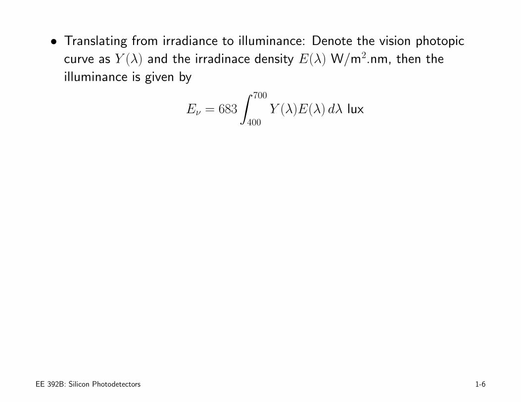
• Translating from irradiance to illuminance: Denote the vision photopic
curve as Y (λ) and the irradinace density E(λ) W/m2.nm, then the
illuminance is given by
Eν = 683
∫ 700
400
Y (λ)E(λ) dλ lux
EE 392B: Silicon Photodetectors 1-6

Photon Flux
• Photon flux F0 is the number of photons per cm2.sec incident on a surface
• Using the photon energy Eph(λ), we can readily translate irradiance
density E(λ) into photon flux
F0 =
∫ 700
400
10−4E(λ)
Eph(λ)dλ photons/cm2.sec
• Translating from illuminance to photon flux:
◦ At λ = 555nm, Eph = 35.8 × 10⁻²⁰Joule; thus 1 lux corresponds to
F0 = 1016/683 × 35.8 = 4.09 × 10¹¹photons/cm2·sec, or, 133 photons
strike a 1µm × 1µm surface per 1/30 sec
◦ A typical light source (e.g., D65) has a wide range of wavelengths
and 1 lux roughly corresponds to F0 ≈ 1012photons/cm2.sec, or, 333
photons strike a 1µm× 1µm surface per 1/30 sec
EE 392B: Silicon Photodetectors 1-7
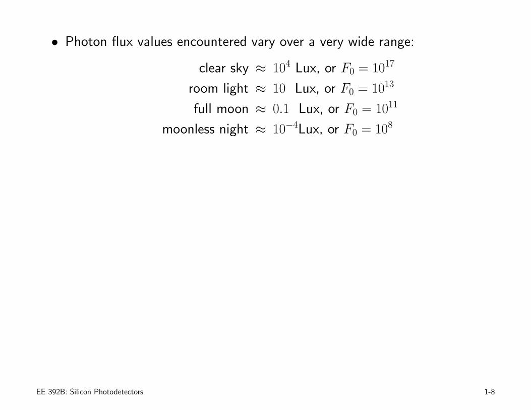
• Photon flux values encountered vary over a very wide range:
clear sky ≈ 104 Lux, or F0 = 1017
room light ≈ 10 Lux, or F0 = 1013
full moon ≈ 0.1 Lux, or F0 = 1011
moonless night ≈ 10−4Lux, or F0 = 108
EE 392B: Silicon Photodetectors 1-8
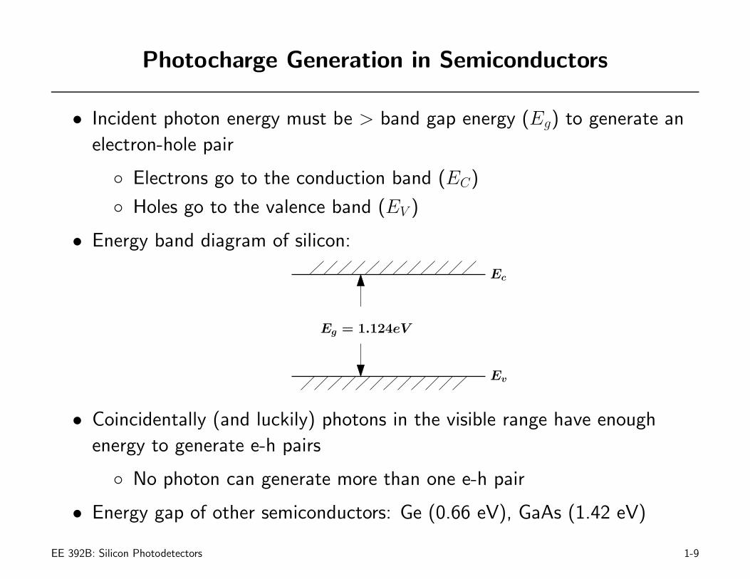
Photocharge Generation in Semiconductors
• Incident photon energy must be > band gap energy (Eg) to generate an
electron-hole pair
◦ Electrons go to the conduction band (EC)
◦ Holes go to the valence band (EV )
• Energy band diagram of silicon:
PSfrag replacements
Ec
Eg = 1.124eV
Ev
• Coincidentally (and luckily) photons in the visible range have enough
energy to generate e-h pairs
◦ No photon can generate more than one e-h pair
• Energy gap of other semiconductors: Ge (0.66 eV), GaAs (1.42 eV)
EE 392B: Silicon Photodetectors 1-9

Photocharge Generation Rate in Silicon
• Assume a monochromatic photon flux F0 photons/cm2.sec at wavelength
λ incident at the surface (i.e., x = 0) of silicon
PSfrag replacements
photon flux
0
silicon
e-h pair
x
• The photon absorption in a material is governed by its absorption
coefficient α(λ) cm−1
• Let F (x) be the photon flux at depth x, then the number of photons
absorbed per second between x and x + ∆x is given by
F (x) − F (x + ∆x) ≈ αF (x)∆x,
EE 392B: Silicon Photodetectors 1-10

We can write this equation in the limit as
dF (x)
dx= −αF (x)
Solving we obtain
F (x) = F0e−αx photons/cm2.sec
Thus the rate of e-h pairs generated at x is
G(x) =d
dx(F0 − F (x)) = αF0e
−αx e-h pair/cm3.sec
EE 392B: Silicon Photodetectors 1-11

Absorption Coefficient of Silicon
200 300 400 500 600 700 800 900 100010
1
102
103
104
105
106
107
PSfrag replacements
Abs
orpt
ion
Coffi
cien
t[c
m−
1]
Wavelength [nm]
E. Palik, ”Handbook of Optical Constant of Solids,” Academic, New York, 1985
EE 392B: Silicon Photodetectors 1-12

Absorption Length of Visible Light in Silicon
EE 392B: Silicon Photodetectors 1-13

Light Absorption in a Silicon Slab
EE 392B: Silicon Photodetectors 1-14

Comments
• F (x) and G(x) are average values assuming a large ensemble of photons
(approaching continuum values)
◦ The photon absorption process is actually discrete and random
• Note that:
◦ 99% of blue light is absorbed within 0.6 µm
◦ 99% of red light is absorbed within 16.6 µm
• These depths (surprisingly) are quite consistent with the junction and well
depths of a CMOS process
• But, this is not the whole story . . .
◦ Photocharge needs to be collected and converted into electrical signal
EE 392B: Silicon Photodetectors 1-15

Photodetectors in Silicon
• A photodetector is used to convert the absorbed photon flux into
photocurrent
• There are three types of photodetectors used, photodiode, which is a
reverse biased pn junction, photogate, and pinned diode
• In a standard CMOS process there are three types of photodiodes available
◦ nwell/psub
◦ n+/psub
◦ p+/nwell
and two types of photogates
◦ nMOS transistor gate to drain
◦ pMOS transistor gate to drain
EE 392B: Silicon Photodetectors 1-16

• In this lecture notes we discuss the photodiode and photogate operation.
The pinned diode will be discussed in the following lecture notes
EE 392B: Silicon Photodetectors 1-17

Photodiode Operation
• Assume the depletion approximation of a reverse biased pn junction
PSfrag replacements photon flux
n-type
p-type
vD > 0
iph
quasi-neutral
quasi-neutraln-region
p-region
depletion
region
• The photocurrent, iph, is the sum of three components:
◦ Current due to electrons generated in the depletion (space charge)
region, iscph
◦ Current due to holes generated in the quasi-neutral n-region, ipph
◦ Current due to electrons generated in the quasi-neutral p-region, inph
EE 392B: Silicon Photodetectors 1-18
• Most electrons generated in the depletion region are converted into
current by strong electric field
• Carriers generated in the quasi-neutral regions need to diffuse to the
depletion region to be collected
◦ Some charge is lost through recombination
◦ The diffusion length determines the fraction of charge that is not
recombined
EE 392B: Silicon Photodetectors 1-19

Photocurrent Derivation
• Assumptions
◦ Abrupt pn junction
◦ Depletion approximation
◦ Low level injection, i.e., flux induced carrier densities << majority
carrier densities
◦ Short base region approximation, i.e., junction depths << diffusion
lengths. This is is quite reasonable for advanced CMOS processes
• Our results are inaccurate but will help us understand the dependence of
iph on various device parameters
References:
• F. Van de Wiele, “Photodiode Quantum Efficiency,” in P. G. Jespers, F. van de Wiele, M. H. White eds. “Solid State Imaging,” p.
47, Noordhoff (1976).
• J.C. Tandon, D.J. Roulston, S.G. Chamberlain, Solid State Electronics, vol. 15, pp. 669 – 685, (1972).
• R.W. Brown, S.G. Chamberlain, Physica Status Solidi (a), vol. 20, pp. 675 – 685 (1973)
EE 392B: Silicon Photodetectors 1-20

• Consider the depletion approximation for a reverse biased pn junction
PSfrag replacements
photon flux
n-type
p-type
v
i
quasi-neutral
quasi-neutraln-region
p-region
depletion
region
x1
x2
x3
x
0
• Assume a monochromatic photon flux F0 photon/cm2·sec incident at the
surface (x = 0), the e-h generation rate at depth x is given by
G(x) = αF0e−αx ph/cm3.sec
• Assuming all generated electrons in the space charge region are collected,
the current density due to generation in the space charge region is
jscph = qF0(e−αx1 − e−αx2) A/cm2,
where q = 1.6 × 10⁻¹⁹Col is the electron charge
EE 392B: Silicon Photodetectors 1-21
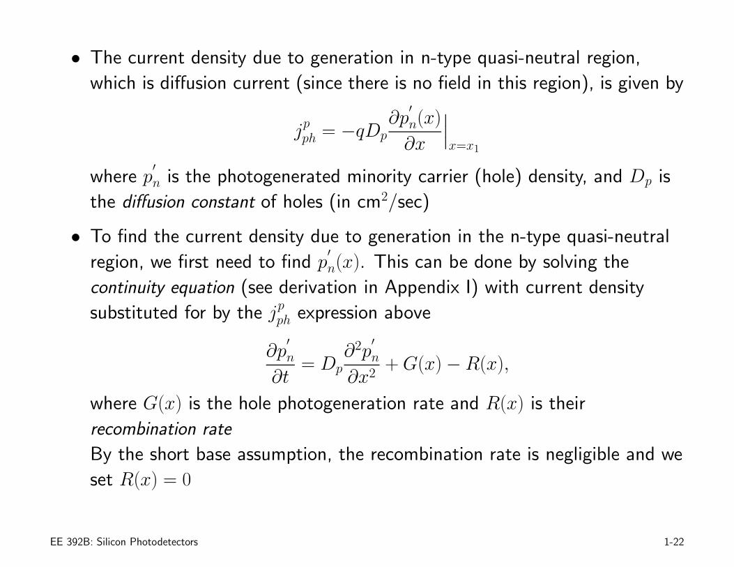
• The current density due to generation in n-type quasi-neutral region,
which is diffusion current (since there is no field in this region), is given by
jpph = −qDp∂p
′
n(x)
∂x
∣
∣
∣
x=x1
where p′
n is the photogenerated minority carrier (hole) density, and Dp is
the diffusion constant of holes (in cm2/sec)
• To find the current density due to generation in the n-type quasi-neutral
region, we first need to find p′
n(x). This can be done by solving the
continuity equation (see derivation in Appendix I) with current density
substituted for by the jpph expression above
∂p′
n
∂t= Dp
∂2p′
n
∂x2+G(x) −R(x),
where G(x) is the hole photogeneration rate and R(x) is their
recombination rate
By the short base assumption, the recombination rate is negligible and we
set R(x) = 0
EE 392B: Silicon Photodetectors 1-22
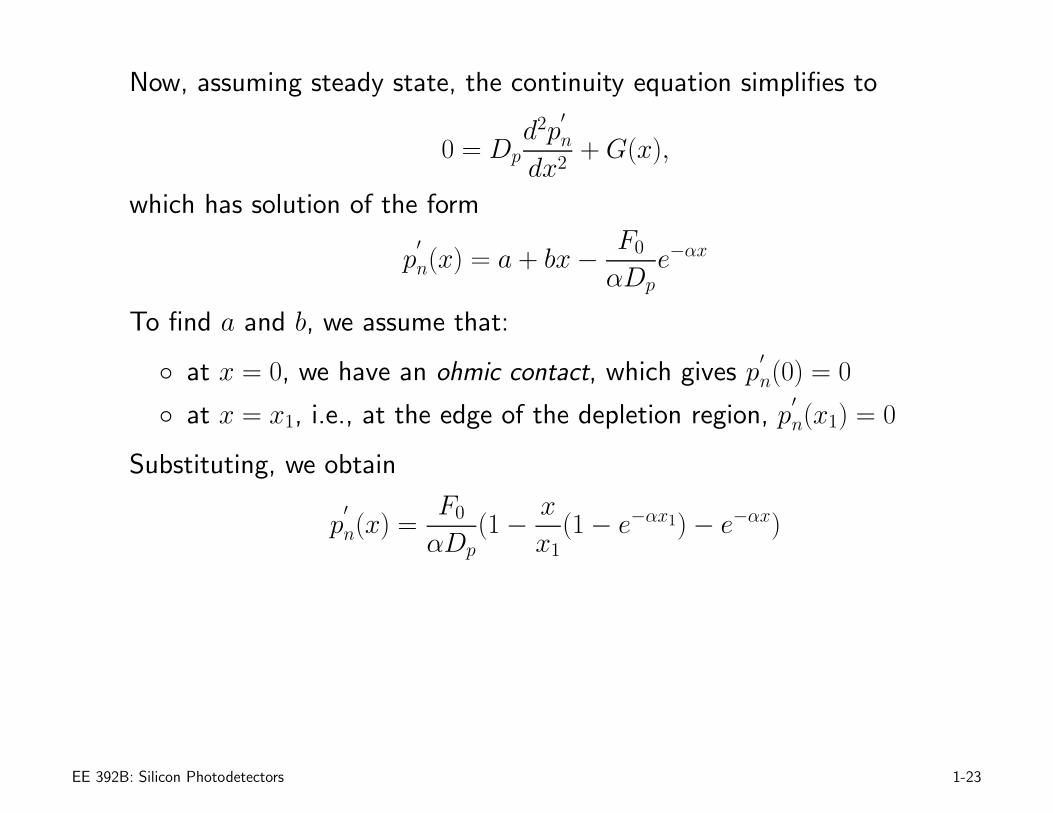
Now, assuming steady state, the continuity equation simplifies to
0 = Dpd2p
′
n
dx2+G(x),
which has solution of the form
p′
n(x) = a + bx−F0
αDpe−αx
To find a and b, we assume that:
◦ at x = 0, we have an ohmic contact, which gives p′
n(0) = 0
◦ at x = x1, i.e., at the edge of the depletion region, p′
n(x1) = 0
Substituting, we obtain
p′
n(x) =F0
αDp(1 −
x
x1(1 − e−αx1) − e−αx)
EE 392B: Silicon Photodetectors 1-23

PSfrag replacements
quasi-neutral
n-region
depletionregion
x1
x
0p
′
n(x)
We can now find the diffusion current density
jpph = −qDp∂p
′
n(x)
∂x
∣
∣
∣
x=x1
=qF0
αx1(1 − (αx1 + 1)e−αx1)
EE 392B: Silicon Photodetectors 1-24

• The current density due to generation in the p-type can be similarly
found, and we obtain
jnph =qF0
α(x3 − x2)((α(x3 − x2) − 1)e−αx2 + e−αx3)
Here we assumed that an ohmic contact at x = x3, which is quite
arbitrary (you will derive it with more reasonable assumptions in HW1)
• The total photogenerated current density is thus given by
jph =qF0
α
(
(1 − e−αx1)
x1−
(e−αx2 − e−αx3)
(x3 − x2)
)
A/cm2
• To find x1 and x2, we can use the simplifying assumptions to derive the
depletion region width (see Appendix II), and we obtain
x2 − x1 =
√
2εsq
(vD + φn + φp)
(
1
Na+
1
Nd
)
,
and use the fact that xn/xp = Na/Nd, where
εs = 10.45 × 10⁻¹³F/cm is the permittivity of Si
Nd and Na are the donor and acceptor densities in cm−3
φn and φp are the potentials in the n and p regions
EE 392B: Silicon Photodetectors 1-25

Example
• Consider the nwell/psub diode in the generic 0.5µm CMOS process
described in Handout 4 with vD = 2V and F0 = 4.09 × 10¹²
photons/cm2·sec at λ = 555nm (room light), find the photocurrent
density components
• Using the depletion equation, we find that x1 = 2 − 0.176 = 1.824µm and
x2 = 3.76µm
The photocurrent density components are
jscph = 120 nA/cm2
jpph = 192 nA/cm2
jnph = 28 nA/cm2
Thus the total photocurrent density jph = 340 nA/cm2
So, for a photodiode of area 30µ2, iph = 102fA
EE 392B: Silicon Photodetectors 1-26
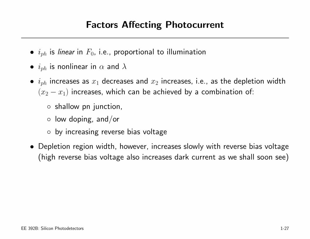
Factors Affecting Photocurrent
• iph is linear in F0, i.e., proportional to illumination
• iph is nonlinear in α and λ
• iph increases as x1 decreases and x2 increases, i.e., as the depletion width
(x2 − x1) increases, which can be achieved by a combination of:
◦ shallow pn junction,
◦ low doping, and/or
◦ by increasing reverse bias voltage
• Depletion region width, however, increases slowly with reverse bias voltage
(high reverse bias voltage also increases dark current as we shall soon see)
EE 392B: Silicon Photodetectors 1-27
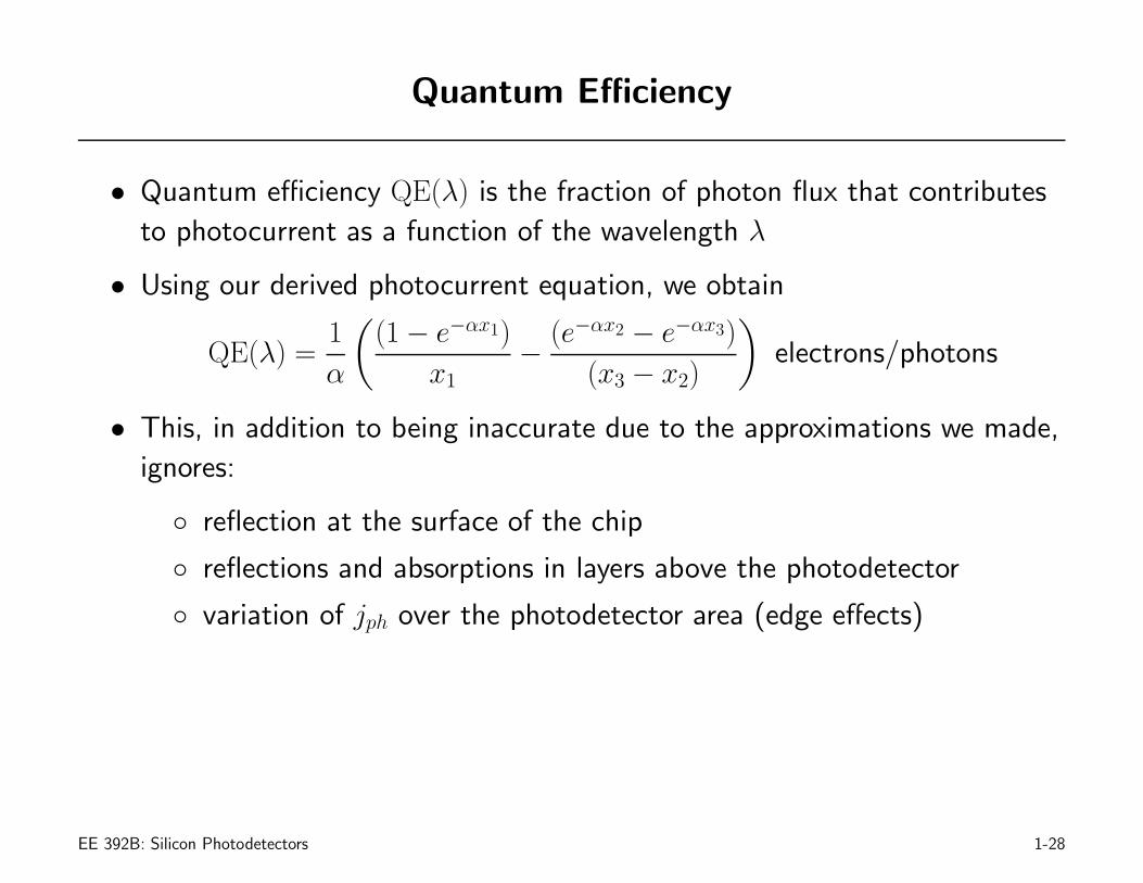
Quantum Efficiency
• Quantum efficiency QE(λ) is the fraction of photon flux that contributes
to photocurrent as a function of the wavelength λ
• Using our derived photocurrent equation, we obtain
QE(λ) =1
α
(
(1 − e−αx1)
x1−
(e−αx2 − e−αx3)
(x3 − x2)
)
electrons/photons
• This, in addition to being inaccurate due to the approximations we made,
ignores:
◦ reflection at the surface of the chip
◦ reflections and absorptions in layers above the photodetector
◦ variation of jph over the photodetector area (edge effects)
EE 392B: Silicon Photodetectors 1-28

Example
Consider the nwell/psub diode with vD = 2V
400 500 600 700 800 900 10000
0.1
0.2
0.3
0.4
0.5
0.6
0.7
PSfrag replacements
Qua
ntum
Effi
cien
cy
Wavelength [nm]
EE 392B: Silicon Photodetectors 1-29
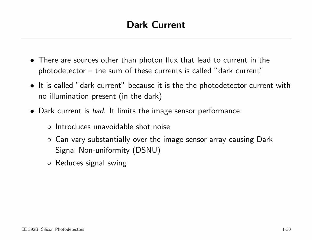
Dark Current
• There are sources other than photon flux that lead to current in the
photodetector – the sum of these currents is called ”dark current”
• It is called ”dark current” because it is the the photodetector current with
no illumination present (in the dark)
• Dark current is bad. It limits the image sensor performance:
◦ Introduces unavoidable shot noise
◦ Can vary substantially over the image sensor array causing Dark
Signal Non-uniformity (DSNU)
◦ Reduces signal swing
EE 392B: Silicon Photodetectors 1-30

Sources of Dark Current
EE 392B: Silicon Photodetectors 1-31
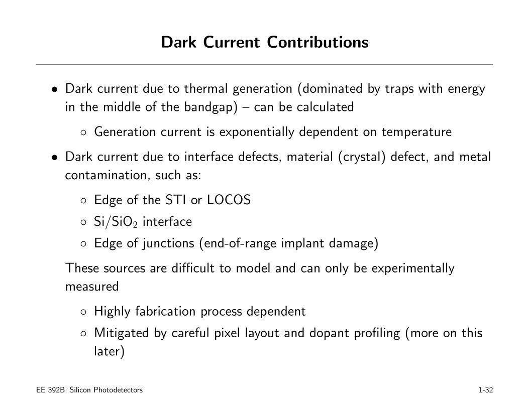
Dark Current Contributions
• Dark current due to thermal generation (dominated by traps with energy
in the middle of the bandgap) – can be calculated
◦ Generation current is exponentially dependent on temperature
• Dark current due to interface defects, material (crystal) defect, and metal
contamination, such as:
◦ Edge of the STI or LOCOS
◦ Si/SiO2 interface
◦ Edge of junctions (end-of-range implant damage)
These sources are difficult to model and can only be experimentally
measured
◦ Highly fabrication process dependent
◦ Mitigated by careful pixel layout and dopant profiling (more on this
later)
EE 392B: Silicon Photodetectors 1-32

Calculation of Generation Dark Current
• Thermally generated dark current density due to bulk defects consists of
three components:
◦ Current due to carrier diffusion from the quasi-neutral regions, jpdcand jndc (vD > 0)
◦ Current due to generation in the space charge region, jscdc
• We first analyze the first two components in the same way we analyzed
jpph and jnph, assuming abrupt pn junction and short base approximation let
pn(x) be the thermally generated minority carriers in the n-type
quasi-neutral region
Ignoring recombination and assuming steady state, the continuity
equation reduces to
0 = Dpd2pn(x)
dx2,
with the general solution
pn(x) = ax+ b
EE 392B: Silicon Photodetectors 1-33

Assuming ohmic contact at x = 0 we get pn(0) = pn0, the minority carrier
concentration at thermal equilibrium, and assuming no free carriers at the
edge of the depletion region, we have pn(x1) = 0
Thus
pn(x) = pn0
(
1 −x
x1
)
PSfrag replacements
photon
n-type
p-type
v
i
quasi-neutral
quasi-neutral
n-region
p-region
depletion
region
x1
x2
x3
x
0 pnpn0
npnp0
xn
xp
EE 392B: Silicon Photodetectors 1-34
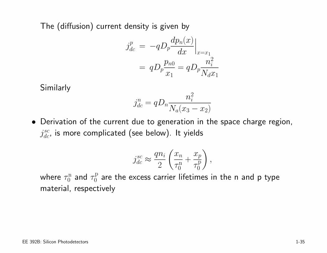
The (diffusion) current density is given by
jpdc = −qDpdpn(x)
dx
∣
∣
∣
x=x1
= qDppn0
x1= qDp
n2i
Ndx1
Similarly
jndc = qDnn2i
Na(x3 − x2)
• Derivation of the current due to generation in the space charge region,
jscdc, is more complicated (see below). It yields
jscdc ≈qni2
(
xnτn0
+xpτp0
)
,
where τ n0 and τp
0 are the excess carrier lifetimes in the n and p type
material, respectively
EE 392B: Silicon Photodetectors 1-35
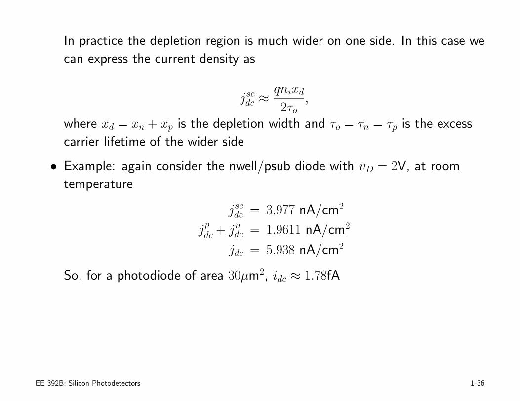
In practice the depletion region is much wider on one side. In this case we
can express the current density as
jscdc ≈qnixd2τo
,
where xd = xn + xp is the depletion width and τo = τn = τp is the excess
carrier lifetime of the wider side
• Example: again consider the nwell/psub diode with vD = 2V, at room
temperature
jscdc = 3.977 nA/cm2
jpdc + jndc = 1.9611 nA/cm2
jdc = 5.938 nA/cm2
So, for a photodiode of area 30µm2, idc ≈ 1.78fA
EE 392B: Silicon Photodetectors 1-36
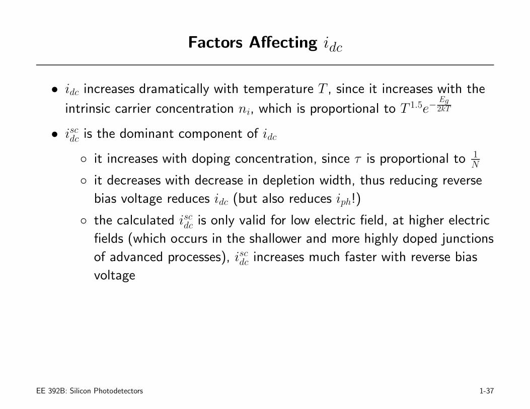
Factors Affecting idc
• idc increases dramatically with temperature T , since it increases with the
intrinsic carrier concentration ni, which is proportional to T 1.5e−Eg2kT
• iscdc is the dominant component of idc
◦ it increases with doping concentration, since τ is proportional to 1N
◦ it decreases with decrease in depletion width, thus reducing reverse
bias voltage reduces idc (but also reduces iph!)
◦ the calculated iscdc is only valid for low electric field, at higher electric
fields (which occurs in the shallower and more highly doped junctions
of advanced processes), iscdc increases much faster with reverse bias
voltage
EE 392B: Silicon Photodetectors 1-37

Generation-Recombination in Depletion Region
• Here, we derive the generation-recombination current in the depletion
region of a reverse biased pn-junction
• The analysis is referred to as the Shockley, Read, Hall (SRH) model
• Salient features of the SRH model:
◦ Generation and recombination of carriers occur through localized
states (recombination centers) with energy within the bandgap
◦ Overall population of the recombination center is fairly constant
◦ Recombination centers quickly capture the majority carriers, but
have to wait for the arrival of a minority carrier
EE 392B: Silicon Photodetectors 1-38

• The generation-recombination rate is given by
U =Ntvthσnσp(pn− n2
i )
σp
[
p + ni exp(
Ei−EtkT
)]
+ σn
[
n + ni exp(
Et−EikT
)]
=(pn− n2
i )
τn
[
p+ ni exp(
Ei−EtkT
)]
+ τp
[
n + ni exp(
Et−EikT
)],
where Nt is the generation-recombination center density, σn,p is the
capture cross section, and the minority carrier lifetimes are given as
τn,p = 1/Ntvthσn,p
We assume that τn = τp ≡ τo (see Handout 4)
Recombination: U > 0
Generation: U < 0
• In the depletion region
n = ni exp
(
Efn − Ei(x)
kT
)
� ni
p = ni exp
(
Ei(x) − Efp
kT
)
� ni
EE 392B: Silicon Photodetectors 1-39
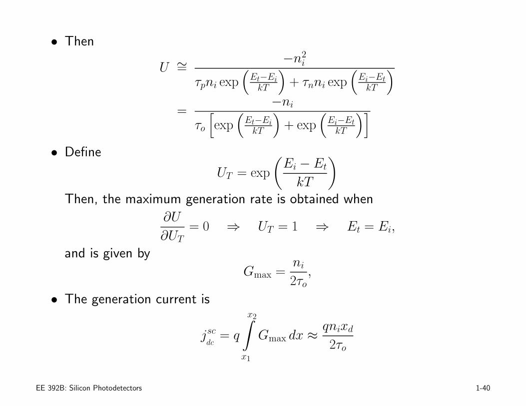
• Then
U ∼=−n2
i
τpni exp(
Et−EikT
)
+ τnni exp(
Ei−EtkT
)
=−ni
τo
[
exp(
Et−EikT
)
+ exp(
Ei−EtkT
)]
• Define
UT = exp
(
Ei − Et
kT
)
Then, the maximum generation rate is obtained when
∂U
∂UT= 0 ⇒ UT = 1 ⇒ Et = Ei,
and is given by
Gmax =ni2τo
,
• The generation current is
jscdc
= q
x2∫
x1
Gmax dx ≈qnixd2τo
EE 392B: Silicon Photodetectors 1-40

Generation Current at Si/SiO2 Surface
• The semiconductor surface has plenty of localized states having energies
within the bandgap
• The kinetics of generation-recombination at the surface is similar to trap
states in the bulk except that the trap density Nst is an areal density (# /
cm2)
• Again, using the SRH model, the surface generation-recombination rate is
given by
Us =Nstvthσnσp(psns − n2
i )
σp
[
ps + ni exp(
Ei−EstkT
)]
+ σn
[
ns + ni exp(
Est−EikT
)]
∼= Nstvthσ(psns − n2
i )[
ps + ns + 2ni cosh(
Ei−EstkT
)],
where again we assumed that σn = σp ≡ σ
Recombination: Us > 0
Generation: Us < 0
EE 392B: Silicon Photodetectors 1-41
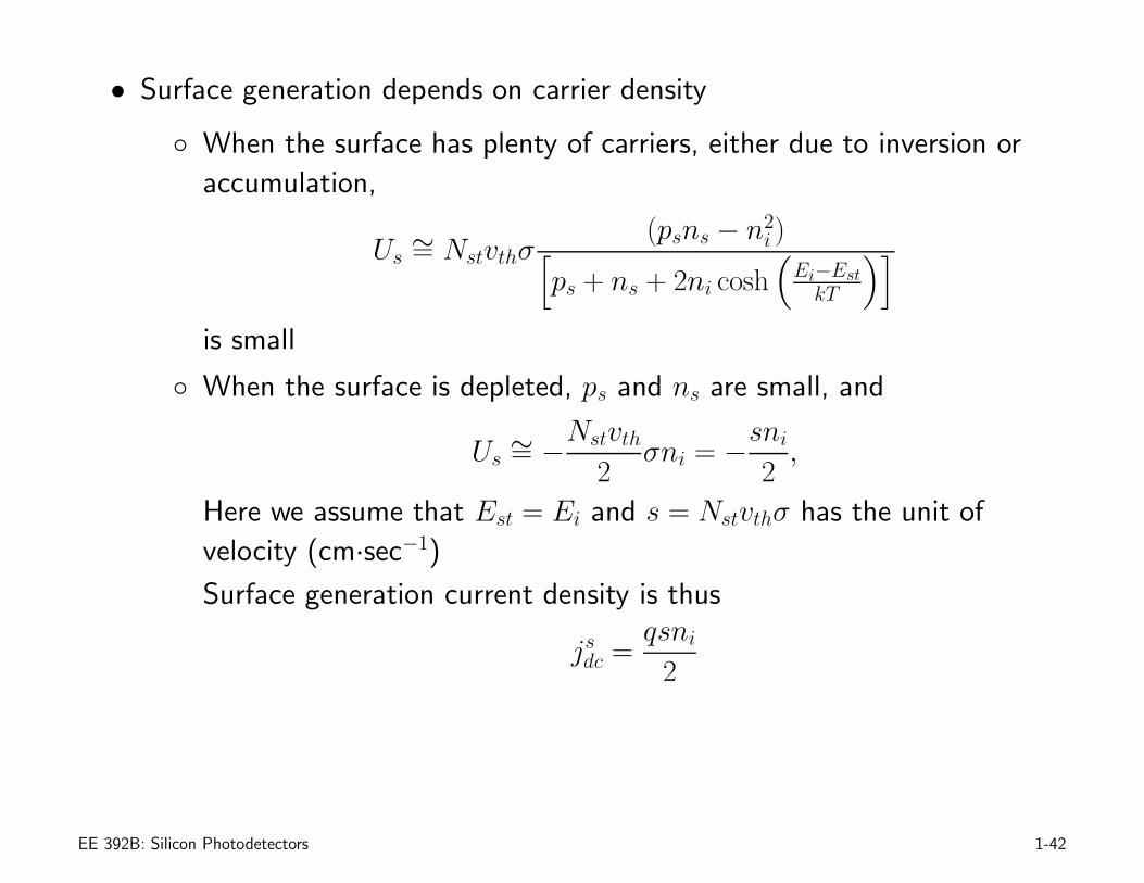
• Surface generation depends on carrier density
◦ When the surface has plenty of carriers, either due to inversion or
accumulation,
Us ∼= Nstvthσ(psns − n2
i )[
ps + ns + 2ni cosh(
Ei−EstkT
)]
is small
◦ When the surface is depleted, ps and ns are small, and
Us ∼= −Nstvth
2σni = −
sni2,
Here we assume that Est = Ei and s = Nstvthσ has the unit of
velocity (cm·sec−1)
Surface generation current density is thus
jsdc =qsni
2
EE 392B: Silicon Photodetectors 1-42

Activation Energy of Dark Current Components
• Notice that the generation currents due to bulk traps and surface traps
are proportional to ni
• And the diffusion current in the quasi-neutral region is proportional to n2i
• Therefore, in a plot of dark current vs log(1/T )
◦ the activation energy of bulk trap and surface trap dark current is Eg
◦ the dark current that is due to diffusion in the quasi-neutral region
has activation energy of Eg/2
EE 392B: Silicon Photodetectors 1-43

Surface Recombination Velocity
• It is difficult to ”derive” the surface recombination velocity
• It is obtained experimentally
EE 392B: Silicon Photodetectors 1-44

• Experimental procedure:
◦ Reverse bias the gated diode
◦ Sweep gate bias from inversion to accumulation
◦ Measure DC current from substrate in inversion (I3), depletion (I2),
and accumulation (I1)
EE 392B: Silicon Photodetectors 1-45

• The currents are given by:
I1 =qniWAB
2τo(diode)+qnisASB
2+qn2
i
NB
√
Dp
τpAB
I2 = I1 +qniWGAG
2τo(gate)+qnisASG
2
I3 = I2 −qnisASG
2
I2 − I3 =qnisASG
2
I3 − I1 =qniWGAG
2τo(gate)
EE 392B: Silicon Photodetectors 1-46

Direct Integration
• As discussed earlier, photocurrent is typically too small to measure directly
• The most commonly used mode of photodiode operation in an image
sensor is direct integration, where the photocurrent (and dark current) are
directly integrated over the diode capacitance
PSfrag replacements
reset
vD
CDiph + idc
vo
QQmax
high lightlow light
tintt
PSfrag replacementsresetvDCD
iph + idcvo
Q
Qmax
high light
low light
tint t
◦ The photodetector is reset to the reverse bias voltage vD
◦ The diode current discharges CD for tint seconds, which is called
integration time or exposure time
◦ At the end of the integration time the accumulated charge Q(tint) (in
electrons) or voltage vo(tint) is read out
EE 392B: Silicon Photodetectors 1-47
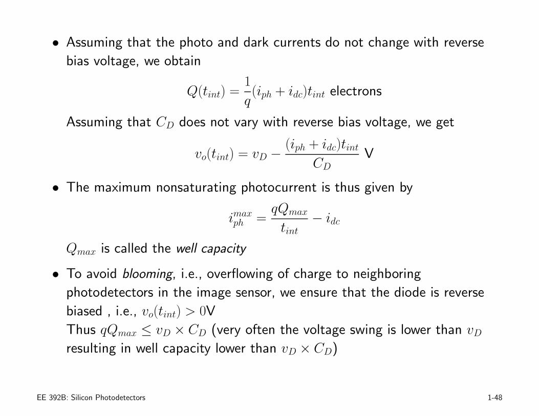
• Assuming that the photo and dark currents do not change with reverse
bias voltage, we obtain
Q(tint) =1
q(iph + idc)tint electrons
Assuming that CD does not vary with reverse bias voltage, we get
vo(tint) = vD −(iph + idc)tint
CDV
• The maximum nonsaturating photocurrent is thus given by
imaxph =qQmax
tint− idc
Qmax is called the well capacity
• To avoid blooming, i.e., overflowing of charge to neighboring
photodetectors in the image sensor, we ensure that the diode is reverse
biased , i.e., vo(tint) > 0V
Thus qQmax ≤ vD × CD (very often the voltage swing is lower than vDresulting in well capacity lower than vD × CD)
EE 392B: Silicon Photodetectors 1-48
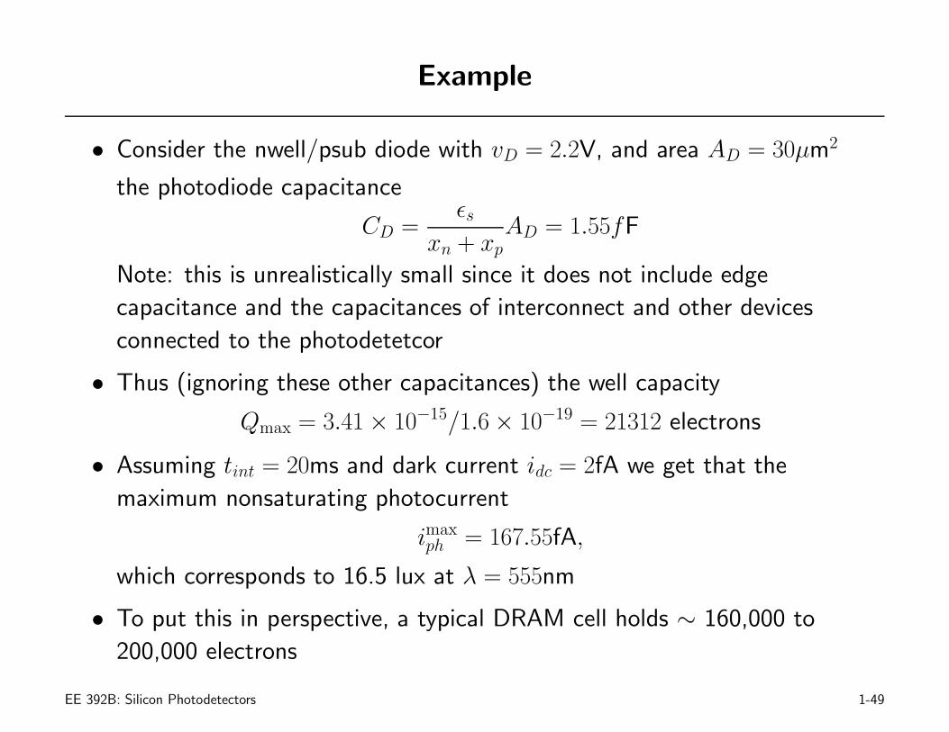
Example
• Consider the nwell/psub diode with vD = 2.2V, and area AD = 30µm2
the photodiode capacitance
CD =εs
xn + xpAD = 1.55fF
Note: this is unrealistically small since it does not include edge
capacitance and the capacitances of interconnect and other devices
connected to the photodetetcor
• Thus (ignoring these other capacitances) the well capacity
Qmax = 3.41 × 10⁻¹⁵/1.6 × 10−19 = 21312 electrons
• Assuming tint = 20ms and dark current idc = 2fA we get that the
maximum nonsaturating photocurrent
imaxph = 167.55fA,
which corresponds to 16.5 lux at λ = 555nm
• To put this in perspective, a typical DRAM cell holds ∼ 160,000 to
200,000 electrons
EE 392B: Silicon Photodetectors 1-49

Finding Q(tint) and vo(tint) Numerically
• Since the depletion region width changes with the reverse bias voltage,
CD, jph, and jdc are not constant during integration
• The output charge and voltage can be found numerically
◦ Set λ and F0 to desired values
◦ Set vo(0) = vD and Q(0) = 0 and calculate vo(k∆t) and Q(k∆t)
iteratively beginning with k = 1 and ending with k = tint∆t
◦ To calculate vo((k + 1)∆t) and Q((k + 1)∆t):
1. Calculate the depletion region width and CkD (using vo(k∆t))
2. Calculate the current densities jph(k∆t) and jdc(k∆t) and the
charge accumulated ∆Qk = (jph(k∆t) + jdc(k∆t))∆t
3. Set vo((k + 1)∆t) = vo(k∆t) − ∆Qk
CkDand
Q((k + 1)∆t) = Q(k∆t) + ∆Qk
• The following graphs provide computed Q(tint) and vo(tint) as a function
of F0 for vD = 2.2V
EE 392B: Silicon Photodetectors 1-50

0 0.5 1 1.5 2 2.5 3 3.5
x 1012
0
1
2
3
4
5
6
7x 10
−9
Photon Flux (photons/cm 2 s)
Pho
to C
harg
e (C
/cm
2 )
nwell/psub Diode, Wavelength=600nm
Direct Integration
EE 392B: Silicon Photodetectors 1-51

0 0.5 1 1.5 2 2.5 3 3.5
x 1012
0
1
2
3
4
5
6x 10
−9
Photon Flux (photons/cm2s)
Tot
al C
harg
e (C
/cm
2 )
nwell/psub Diode, Wavelength=600nm
Direct Integration
EE 392B: Silicon Photodetectors 1-52

0 0.5 1 1.5 2 2.5 3 3.5
x 1012
1
1.2
1.4
1.6
1.8
2
2.2
2.4
Photon Flux (photons/cm2 s)
Fin
al v
olta
ge d
ue to
pho
toch
arge
(V
)
nwell/psub Diode, Wavelength=600nm
Direct Integration
EE 392B: Silicon Photodetectors 1-53

0 0.5 1 1.5 2 2.5 3 3.5
x 1012
1
1.1
1.2
1.3
1.4
1.5
1.6
1.7
1.8
1.9
2
Photon Flux (photons/cm2s)
Fin
al to
tal v
olta
ge o
n di
ode
(V)
nwell/psub Diode, Wavelength=600nm
Direct Integration
EE 392B: Silicon Photodetectors 1-54
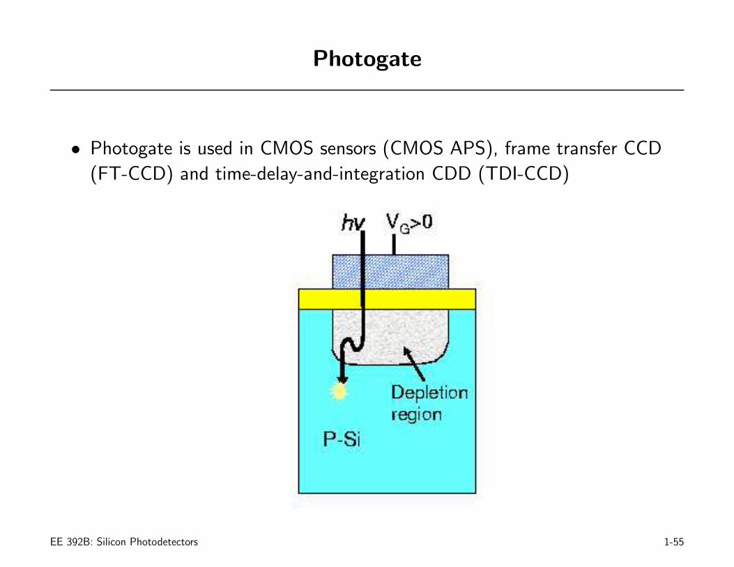
Photogate
• Photogate is used in CMOS sensors (CMOS APS), frame transfer CCD
(FT-CCD) and time-delay-and-integration CDD (TDI-CCD)
EE 392B: Silicon Photodetectors 1-55

Photogate Operation
• Gate voltage vG is set high enough to bias the MOS capacitor into the
deep depletion regime (this requires vG >> vT) (see Appendix)
• Electrons generated in the depletion region are collected in the potential
well
• Electrons generated in the quasi-neutral region will
◦ Recombine with holes
◦ Diffuse to depletion region and get collected in the potential well if it
is within the diffusion length of the minority carriers
• Holes will be collected in the substrate
• How many of the photo-generated carriers are collected depends on:
◦ Diffusion length of minority carriers
◦ Location and length of the depletion region
EE 392B: Silicon Photodetectors 1-56

EE 392B: Silicon Photodetectors 1-57

Quantum Efficiency of Photogate
• Photocurrent has two components
◦ Current due to generation in the depletion region, iscph, again almost
all carriers contribute to the current
◦ Diffusion current due to generation in the quasi-neutral p-region, inph
• To calculate the current we make the depletion approximation and use the
basic MOS capacitor equations to find the depletion region width (see
Appendix III) (you will derive it in HW2)
• A disadvantage of the photogate is lower quantum efficiency, especially
for shorter wavelengths (blue), due to absorption in the polysilicon gate
(which has the same α as crystalline silicon)
• Photogate is also used in direct integration mode; charge accumulated on
gate is transferred to another capacitor (as we shall see later)
EE 392B: Silicon Photodetectors 1-58

Quantum Efficiency of Photogate
• It can be shown that QE for photogate, not including absorption in the
polysilicon gate, is given by
QE(λ) = 1−e−αxd+αL2
n
α2L2n − 1
(
αe−αxd +e−αL − e−αxd cosh ((L− xd)/Ln)
Ln sinh ((L− xd)/Ln)
)
• Limiting Cases:
◦ Very long diffusion length (Ln → ∞):
QE = 1 − e−αxd + e−αxd(
1 −1 − e−α(L−xd)
α(L− xd)
)
◦ Very thick substrate (L→ ∞):
QE = 1 − e−αxd +αLne
−αxd
(αLn + 1)
EE 392B: Silicon Photodetectors 1-59

EE 392B: Silicon Photodetectors 1-60

Appendix I – Derivation of 1-D Continuity Equation
• Consider minority carrier (electron) current flow in p-type silicon
• In a slab x to x + ∆x
PSfrag replacements
jn(x) jn(x+ ∆x)
Gn(x)
Rn(x)x x+ ∆x
Ec
Ev
jn(x): electron current density at x
Gn(x): generation rate (electrons/cm3·s)
Rn(x): recombination rate (electrons/cm3·s)
n(x): electron density at x (electrons/cm3)
EE 392B: Silicon Photodetectors 1-61

• The rate of electron density increase in the slab
∂n(x)
∂t∆x ≈ −
1
q(jn(x) − jn(x + ∆x)) + (Gn(x) −Rn(x))∆x,
which in the limit, gives
∂n(x)
∂t=
1
q
∂jn(x)
∂x+ (Gn(x) −Rn(x))
assuming no electric field, the current is only due to diffusion and is given
by
jn(x) = qDn∂n(x)
∂x,
where Dn is the diffusion constant for electrons in cm2/s
substituting, we get the continuity equation
∂n(x)
dt= Dn
∂2n(x)
∂x2+ (Gn(x) − Rn(x))
• Similarly for holes,
jp(x) = −qDp∂p(x)
∂xand the continuity equation is
∂p(x)
∂t= Dp
∂2p(x)
∂x2+ (Gp(x) −Rp(x))
EE 392B: Silicon Photodetectors 1-62

• Assuming low level injection, i.e., that excess carrier concentration <<
majority carrier concentration, we get that
Rn =np − np0
τn
where np0 is the intrinsic minority carrier concentration, and τn is the
carrier lifetime
EE 392B: Silicon Photodetectors 1-63

Appendix II – Depletion Width for PN Junction
• Energy band diagrams at thermal equilibriumPSfrag replacements
qφp
qφn
Ec Ec
Ei EiEfp
Ev Ev
Efn
n-typep-type
Here φn = kTq ln Nd
niand φp = kT
q ln Nani
, where
k = 8.62 × 10⁻⁵eV K−1 is the Boltzman constant
T is the temperature in Kelvin
q = 1.6 × 10⁻¹⁹Col is the electron charge
ni is the intrinsic carrier concentration ≈ 1.45 × 1010cm−3 at room
temperature
Nd and Na are the donor and acceptor densities in cm−3
EE 392B: Silicon Photodetectors 1-64

PN Junction Energy Band Diagram
• The energy band diagram for reverse biased pn junction
PSfrag replacements
qφp
qφn
Ec
Ei
Efp
Ev
Efn
qvD
p-type n-type
ρ col/cm3
−xpxn
−qNa
qNd
x
x
x
E V/cm
Emax
φ V
EE 392B: Silicon Photodetectors 1-65

E and φ are found by solving the Poisson equation
d2φ
dx2= −
dE
dx= −
ρ(x)
εs,
where εs = 10.45 × 10⁻¹³F/cm is the permittivity of Si
So in the p-type region, we obtain
E(x) = −qNa
εs(x + xp)
and
Emax = −qNa
εsxp
Similarly, in the n-type region we have
E(x) =qNd
εs(x− xn)
and
Emax = −qNd
εsxn
Thusxnxp
=Na
Nd
EE 392B: Silicon Photodetectors 1-66

Now
φ(xn) = −
∫ xn
−xp
Edx
=qNdx
2n
2εs+qNax
2p
2εs= vD + φn + φp
Combining the last two equations, we obtain that the depletion width
xd = xn + xp =
√
2εsq
(vD + φn + φp)(1
Na+
1
Nd)
• Example (nwell/psub diode): assuming vD = 2V, φn = 0.3486V, and
φp = 0.289V, we get xn = 0.176µm and xp = 1.76µm
• The (small signal) diode capacitance per unit area is defined as
C =dQ
dvD,
where the charge Q = qNdxn = qNaxp. Thus,
C =εs
xn + xpF/cm2
For the previous example C = 5.4 × 10⁻⁹F/cm2
EE 392B: Silicon Photodetectors 1-67

Appendix III – MOS Capacitor
• First consider the energy band diagrams under thermal equilibrium for
polysilicon, oxide, and silicon
polsilicon
PSfrag replacements
0.95eV
4.05eV
qφp
E0Ec
Ec
Ei
Ef
Ev
Ef ≈ Ec
polysilicon
oxide p-type
E0 is the free electron energy
E0 − Ec = 4.05eV is the semiconductor electron affinity
E0 − E oxidec = 0.95eV is the oxide electron affinity
EE 392B: Silicon Photodetectors 1-68

• The energy band diagram for the MOS system under thermal equilibrium
assuming vG = 0
PSfrag replacements
qv0
3.1eV
3.1eV Ec
EiEf
Ev
qφp
qψs0tox
poly oxide p-type
ρ
Q
−Q
0 xd x
−qNa
EE 392B: Silicon Photodetectors 1-69

We can find v0, ψ0, and xd by writing the flat-band voltage in two ways
and solving the Poisson equation
vFB =Eg
2q+ φp = v0 + ψs0,
v0 =qNaxdCox
, and
ψs0 =qNax
2d
2εsCox = εox
toxF/cm2, and εox = 34.5 × 10⁻¹⁴F/cm
• Energy band diagram in the deep depletion regimePSfrag replacements
qv0
EcEiEf
Ef
qvG
Ev
qψs
tox
poly oxide p-type
EE 392B: Silicon Photodetectors 1-70
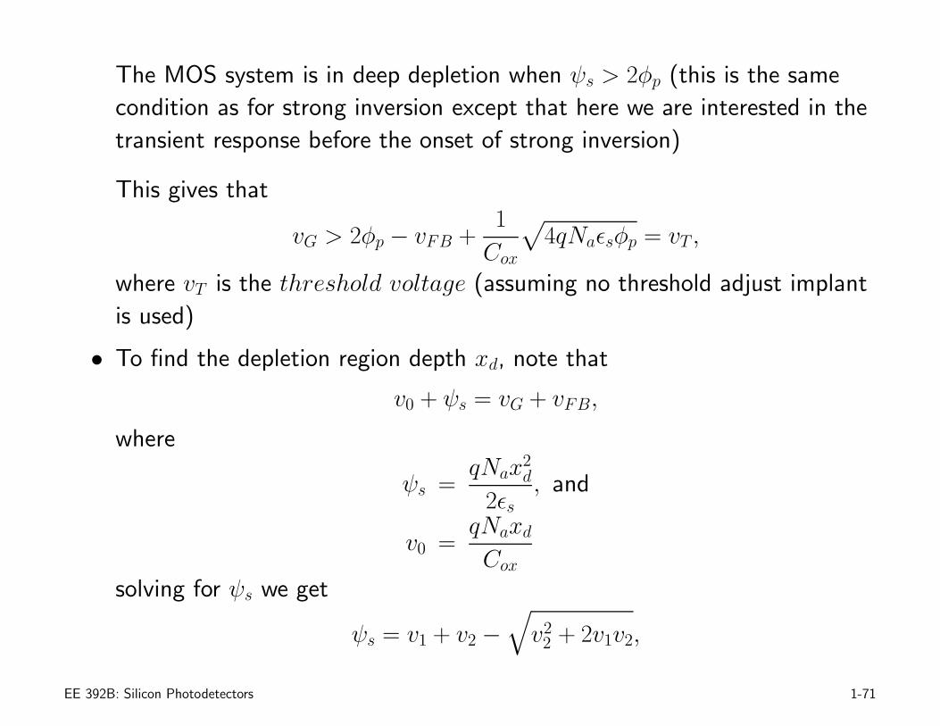
The MOS system is in deep depletion when ψs > 2φp (this is the same
condition as for strong inversion except that here we are interested in the
transient response before the onset of strong inversion)
This gives that
vG > 2φp − vFB +1
Cox
√
4qNaεsφp = vT ,
where vT is the threshold voltage (assuming no threshold adjust implant
is used)
• To find the depletion region depth xd, note that
v0 + ψs = vG + vFB,
where
ψs =qNax
2d
2εs, and
v0 =qNaxdCox
solving for ψs we get
ψs = v1 + v2 −
√
v22 + 2v1v2,
EE 392B: Silicon Photodetectors 1-71

where
v1 = vG + vFB, and
v2 =qNaεsC2ox
the depletion width can then be determined
Note: for the MOS capacitor to stay in the deep depletion we set vD = ψs
EE 392B: Silicon Photodetectors 1-72

Appendix IV
Bulk Mobility
EE 392B: Silicon Photodetectors 1-73

Minority Carrier Diffusion Length
EE 392B: Silicon Photodetectors 1-74
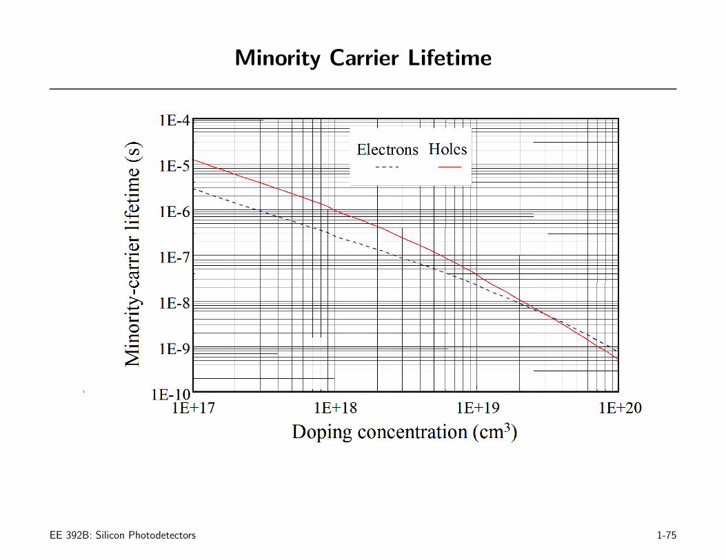
Minority Carrier Lifetime
EE 392B: Silicon Photodetectors 1-75


![Characterization Test of New Generation Low Cross-Talk MPPCs · PSAU Power Supply and Amplification Unit APPLICABLE DOCUMENTS [AD1] AD1 ... photon flux intensity coming into the integrating](https://static.fdocuments.us/doc/165x107/5e7b19f6bdfd9c7e331a3740/characterization-test-of-new-generation-low-cross-talk-psau-power-supply-and-amplification.jpg)