LHF64P01 - Digi-Key Sheets/Sharp PDFs...LHF64P01 1 CONTENTS PAGE 56-Lead TSOP (Normal Bend) Pinout 3...
45
Transcript of LHF64P01 - Digi-Key Sheets/Sharp PDFs...LHF64P01 1 CONTENTS PAGE 56-Lead TSOP (Normal Bend) Pinout 3...


LHF64P01
• Handle this document carefully for it contains material protected by international copyright law. Any reproduction,full or in part, of this material is prohibited without the express written permission of the company.
• When using the products covered herein, please observe the conditions written herein and the precautions outlined inthe following paragraphs. In no event shall the company be liable for any damages resulting from failure to strictlyadhere to these conditions and precautions.
(1) The products covered herein are designed and manufactured for the following application areas. When using theproducts covered herein for the equipment listed in Paragraph (2), even for the following application areas, be sureto observe the precautions given in Paragraph (2). Never use the products for the equipment listed in Paragraph(3).
• Office electronics• Instrumentation and measuring equipment• Machine tools• Audiovisual equipment• Home appliance• Communication equipment other than for trunk lines
(2) Those contemplating using the products covered herein for the following equipment which demands highreliability, should first contact a sales representative of the company and then accept responsibility forincorporating into the design fail-safe operation, redundancy, and other appropriate measures for ensuringreliability and safety of the equipment and the overall system.
• Control and safety devices for airplanes, trains, automobiles, and other transportation equipment• Mainframe computers• Traffic control systems• Gas leak detectors and automatic cutoff devices• Rescue and security equipment• Other safety devices and safety equipment, etc.
(3) Do not use the products covered herein for the following equipment which demands extremely high performancein terms of functionality, reliability, or accuracy.
• Aerospace equipment• Communications equipment for trunk lines• Control equipment for the nuclear power industry• Medical equipment related to life support, etc.
(4) Please direct all queries and comments regarding the interpretation of the above three Paragraphs to a salesrepresentative of the company.
• Please direct all queries regarding the products covered herein to a sales representative of the company.
Rev. 0.06

LHF64P01 1
CONTENTS
PAGE
56-Lead TSOP (Normal Bend) Pinout ....................... 3
Pin Descriptions.......................................................... 4
CE0, CE1, CE2 Truth Table ....................................... 5
Memory Map.............................................................. 6
Identifier Codes Address ............................................ 7
OTP Block Address Map............................................ 8
Bus Operation............................................................. 9
Command Definitions .............................................. 10
Functions of Block Lock .......................................... 12
Status Register Definition......................................... 13
Extended Status Register Definition ........................ 14
STS Configuration Definition .................................. 15
PAGE
1 Electrical Specifications ........................................ 16
1.1 Absolute Maximum Ratings........................... 16
1.2 Operating Conditions ..................................... 16
1.2.1 Capacitance.............................................. 17
1.2.2 AC Input/Output Test Conditions............ 17
1.2.3 DC Characteristics................................... 18
1.2.4 AC Characteristics - Read-Only Operations .............................. 20
1.2.5 AC Characteristics - Write Operations.... 24
1.2.6 Reset Operations...................................... 26
1.2.7 Block Erase, (Page Buffer) Program and Block Lock Configuration Performance.............................................. 27
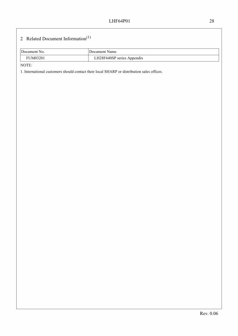
2 Related Document Information ............................. 28
3 Package and packing specification........................ 29
Rev. 0.06

LHF64P01 2
LH28F640SPHT-PTL1264Mbit (4Mbit×16/8Mbit×8)Page Mode Flash MEMORY
64-Mbit Density• Bit Organization ×8/×16
High Performance Page Mode Reads for Memory Array• 120/25ns 4-Word/ 8-Byte Page Mode
VCC=2.7V-3.6V Operation• VCCQ for Input/Output Power Supply Isolation• Automatic Power Savings Mode reduces ICCR
in Static Mode
OTP (One Time Program) Block• 4-Word/ 8-Byte Factory-Programmed Area• 3963-Word/ 7926-Byte User-Programmable Area
High Performance Program with Page Buffer• 16-Word/ 32-Byte Page Buffer• Page Buffer Program Time 12.5µs/byte (Typ.)
Operating Temperature -40°C to +85°C
Symmetrically-Blocked Architecture• Sixty-four 64-KWord/ 128-KByte Blocks
Enhanced Data Protection Features• Individual Block Lock• Absolute Protection with VPEN≤VPENLK
• Block Erase, (Page Buffer) Program Lockout duringPower Transitions
Automated Erase/Program Algorithms• Program Time 210µs (Typ.)• Block Erase Time 1s (Typ.)
Cross-Compatible Command Support• Basic Command Set• Common Flash Interface (CFI)
Extended Cycling Capability• Minimum 100,000 Block Erase Cycles
56-Lead TSOP (Normal Bend)
CMOS Process (P-type silicon substrate)
ETOXTM* Flash Technology
Not designed or rated as radiation hardened
The product, which is Page Mode Flash memory, is a high density, low cost, nonvolatile read/write storage solution for awide range of applications. The product can operate at VCC=2.7V-3.6V and VPEN=2.7V-3.6V
The product supports high performance page mode. It allows code execution directly from Flash, thus eliminating timeconsuming wait states.
Fast program capability is provided through the use of high speed Page Buffer Program.
The block locking scheme is available for memory array and this scheme provides maximum flexibility for safe nonvolatilecode and data storage.
OTP (One Time Program) block provides an area to store security code and to protect its code.
* ETOX is a trademark of Intel Corporation.
Rev. 0.06
LHF64P01 3
567
891011121314151617181920
212223242526
2728
525150494847
4645444342414039
3837363534333231
3029
56-LEAD TSOPSTANDARD PINOUT
14mm x 20mmTOP VIEW
A19
A18
A17
A16
VCC
A15
A14
A13
A12
CE0
VPEN
RP#A11
A10
A9
A8
GNDA7
A6
A5
A4
A3
A2
A1
WE#OE#STSDQ15
DQ7
DQ14
DQ6
DQ13
DQ5
DQ12
DQ4
VCCQ
GNDDQ11
DQ3
DQ10
VCC
DQ9
DQ1
DQ8
DQ0
A0
BYTE#NC
123
4
56555453
A22
CE1
A21
A20
CE2
DQ2
GND
NC
Figure 1. 56-Lead TSOP (Normal Bend) Pinout
Rev. 0.06

LHF64P01 4
Table 1. Pin Descriptions
Symbol Type Name and Function
A0 INPUTADDRESS INPUTS: Lowest address input in byte mode (BYTE#=VIL : ×8 bit).Address is internally latched during an erase or a program cycle. This pin is not used inword mode (BYTE#=VIH : ×16 bit)
A22-A1 INPUTADDRESS INPUTS: Inputs for addresses during read, erase and program operations. Addresses are internally latched during an erase or a program cycle.
DQ15-DQ0INPUT/
OUTPUT
DATA INPUTS/OUTPUTS: Inputs data and commands during CUI (Command UserInterface) write cycles, outputs data during memory array, status register, query code,identifier code reads. Data pins float to high-impedance (High Z) when the chip oroutputs are deselected. Data is internally latched during an erase or program cycle.DQ15-DQ8 pins are not used in byte mode (BYTE#=VIL : ×8 bit).
CE0, CE1, CE2
INPUT
CHIP ENABLE: Activates the device’s control logic, input buffers, decoders and senseamplifiers. When the device is de-selected, power consumption reduces to standbylevels. Refer to Table 2 to determine whether the device is selected or de-selecteddepending on the state of CE0, CE1 and CE2.
RP# INPUT
RESET: When low (VIL), RP# resets internal automation and inhibits erase and programoperations, which provides data protection. RP#-high (VIH) enables normal operation.After power-up or reset mode, the device is automatically set to read array mode. RP# must be low during power-up/down.
OE# INPUT OUTPUT ENABLE: Gates the device’s outputs during a read cycle.
WE# INPUTWRITE ENABLE: Controls writes to the CUI and array blocks. Addresses and data arelatched on the first edge of CE0, CE1 or CE2 that disables the device or the rising edge ofWE# (whichever occurs first).
STSOPEN DRAIN
OUTPUT
STATUS: Indicates the status of the internal WSM (Write State Machine). Whenconfigured in level mode (default mode), STS acts as a RY/BY# pin (STS is VOL whenthe WSM is executing internal erase or program algorithms). When configured in one ofits pulse modes, STS can pulse to indicate erase/program completion. Refer to Table 9for STS configuration.
BYTE# INPUT
BYTE ENABLE: BYTE# VIL places the device in byte mode (×8). In this mode, DQ15-DQ8 is floated (High Z) and A0 is the lowest address input. BYTE# VIH places thedevice in word mode (×16) and A1 is the lowest address input.
VPEN INPUTMONITORING POWER SUPPLY VOLTAGE: VPEN is not used for power supply pin.With VPEN≤VPENLK, block erase, (page buffer) program, block lock configuration andOTP program cannot be executed and should not be attempted.
VCC SUPPLYDEVICE POWER SUPPLY (2.7V-3.6V): With VCC≤VLKO, all write attempts to theflash memory are inhibited. Device operations at invalid VCC voltage (refer to DCCharacteristics) produce spurious results and should not be attempted.
VCCQ SUPPLYINPUT/OUTPUT POWER SUPPLY (2.7V-3.6V): Power supply for all input/outputpins.
GND SUPPLY GROUND: Do not float any ground pins.
NC NO CONNECT: Lead is not internally connected; it may be driven or floated.
Rev. 0.06

LHF64P01 5
NOTE:1. For single-chip applications, CE1 and CE2 can be connected to GND.
Table 2. CE0, CE1, CE2 Truth Table (1)
CE2 CE1 CE0 Device
VIL VIL VIL Enabled
VIL VIL VIH Disabled
VIL VIH VIL Disabled
VIL VIH VIH Disabled
VIH VIL VIL Enabled
VIH VIL VIH Enabled
VIH VIH VIL Enabled
VIH VIH VIH Disabled
Rev. 0.06
LHF64P01 6
64-Kword/128-Kbyte Block 63
64-Kword/128-Kbyte Block 62
64-Kword/128-Kbyte Block 61
64-Kword/128-Kbyte Block 60
64-Kword/128-Kbyte Block 59
64-Kword/128-Kbyte Block 58
64-Kword/128-Kbyte Block 57
64-Kword/128-Kbyte Block 56
64-Kword/128-Kbyte Block 55
64-Kword/128-Kbyte Block 54
64-Kword/128-Kbyte Block 53
64-Kword/128-Kbyte Block 52
64-Kword/128-Kbyte Block 51
64-Kword/128-Kbyte Block 50
64-Kword/128-Kbyte Block 49
64-Kword/128-Kbyte Block 48
64-Kword/128-Kbyte Block 47
64-Kword/128-Kbyte Block 46
64-Kword/128-Kbyte Block 45
64-Kword/128-Kbyte Block 44
64-Kword/128-Kbyte Block 43
64-Kword/128-Kbyte Block 42
64-Kword/128-Kbyte Block 41
64-Kword/128-Kbyte Block 40
64-Kword/128-Kbyte Block 39
64-Kword/128-Kbyte Block 38
64-Kword/128-Kbyte Block 37
64-Kword/128-Kbyte Block 36
64-Kword/128-Kbyte Block 35
64-Kword/128-Kbyte Block 34
64-Kword/128-Kbyte Block 33
64-Kword/128-Kbyte Block 32
64-Kword/128-Kbyte Block 31
64-Kword/128-Kbyte Block 30
64-Kword/128-Kbyte Block 29
64-Kword/128-Kbyte Block 28
64-Kword/128-Kbyte Block 27
64-Kword/128-Kbyte Block 26
64-Kword/128-Kbyte Block 25
64-Kword/128-Kbyte Block 24
64-Kword/128-Kbyte Block 23
64-Kword/128-Kbyte Block 22
64-Kword/128-Kbyte Block 21
64-Kword/128-Kbyte Block 20
64-Kword/128-Kbyte Block 19
64-Kword/128-Kbyte Block 18
64-Kword/128-Kbyte Block 17
64-Kword/128-Kbyte Block 16
64-Kword/128-Kbyte Block 15
64-Kword/128-Kbyte Block 14
64-Kword/128-Kbyte Block 13
64-Kword/128-Kbyte Block 12
64-Kword/128-Kbyte Block 11
64-Kword/128-Kbyte Block 10
64-Kword/128-Kbyte Block 9
64-Kword/128-Kbyte Block 8
64-Kword/128-Kbyte Block 7
64-Kword/128-Kbyte Block 6
64-Kword/128-Kbyte Block 5
64-Kword/128-Kbyte Block 4
64-Kword/128-Kbyte Block 3
64-Kword/128-Kbyte Block 2
64-Kword/128-Kbyte Block 1
64-Kword/128-Kbyte Block 0
[A22-A1][A22-A1] [A22-A0][A22-A0]
000000
02000003FFFF
01FFFF
04000005FFFF06000007FFFF08000009FFFF0A00000BFFFF0C00000DFFFF0E00000FFFFF10000011FFFF12000013FFFF14000015FFFF16000017FFFF18000019FFFF1A00001BFFFF1C00001DFFFF1E00001FFFFF20000021FFFF22000023FFFF24000025FFFF26000027FFFF28000029FFFF2A00002BFFFF
2E00002FFFFF30000031FFFF32000033FFFF34000035FFFF36000037FFFF38000039FFFF3A00003BFFFF3C00003DFFFF3E00003FFFFF
2C00002DFFFF
000000
01000001FFFF
00FFFF
02000002FFFF03000003FFFF04000004FFFF05000005FFFF06000006FFFF07000007FFFF08000008FFFF09000009FFFF0A00000AFFFF0B00000BFFFF0C00000CFFFF0D00000DFFFF0E00000EFFFF0F00000FFFFF10000010FFFF11000011FFFF12000012FFFF13000013FFFF14000014FFFF15000015FFFF
17000017FFFF18000018FFFF19000019FFFF1A00001AFFFF1B00001BFFFF1C00001CFFFF1D00001DFFFF1E00001EFFFF1F00001FFFFF
16000016FFFF
200000
21000021FFFF
20FFFF
22000022FFFF23000023FFFF24000024FFFF25000025FFFF26000026FFFF27000027FFFF28000028FFFF29000029FFFF2A00002AFFFF2B00002BFFFF2C00002CFFFF2D00002DFFFF2E00002EFFFF2F00002FFFFF30000030FFFF31000031FFFF32000032FFFF33000033FFFF34000034FFFF35000035FFFF
37000037FFFF38000038FFFF39000039FFFF3A00003AFFFF3B00003BFFFF3C00003CFFFF3D00003DFFFF3E00003EFFFF3F00003FFFFF
36000036FFFF
400000
42000043FFFF
41FFFF
44000045FFFF46000047FFFF48000049FFFF4A00004BFFFF4C00004DFFFF4E00004FFFFF50000051FFFF52000053FFFF54000055FFFF56000057FFFF58000059FFFF5A00005BFFFF5C00005DFFFF5E00005FFFFF60000061FFFF62000063FFFF64000065FFFF66000067FFFF68000069FFFF6A00006BFFFF
6E00006FFFFF70000071FFFF72000073FFFF74000075FFFF76000077FFFF78000079FFFF7A00007BFFFF7C00007DFFFF7E00007FFFFF
6C00006DFFFF
Rev. 0.06
Figure 2. Memory Map

LHF64P01 7
NOTES:1. The address A0 don't care.2. "00H" is presented on DQ15-DQ8 in word mode (BYTE#=VIH : ×16 bit).3. Block Address = The beginning location of a block address. DQ15-DQ1 are reserved for future implementation.
Table 3. Identifier Codes Address
CodeAddress
[A22-A1] (1)Data
[DQ7-DQ0] Notes
Manufacturer Code Manufacturer Code 000000H B0H 2
Device Code Device Code 000001H 17H 2
Block Lock ConfigurationCode
Block is Unlocked BlockAddress
+ 2
DQ0 = 0 3
Block is Locked DQ0 = 1 3
Rev. 0.06

LHF64P01 8
Rev. 0.06
Customer Programmable Area Lock Bit (DQ1)Factory Programmed Area Lock Bit (DQ0)
Customer Programmable Area
Factory Programmed Area
Reserved for Future Implementation000080H
000081H
000084H
000085H
000FFFH
[A22-A1]
(DQ15-DQ2) 000100H
000102H
000109H
00010AH
001FFFH
[A22-A0]
Figure 3. OTP Block Address Map(The area not specified in the above figure cannot be used.)

LHF64P01 9
Rev. 0.06
NOTES:1. Refer to DC Characteristics. When VPEN≤VPENLK, memory contents can be read, but cannot be altered.2. X can be VIL or VIH for control pins and addresses, and VPENLK or VPENH for VPEN.
Refer to DC Characteristics for VPENLK and VPENH voltages.3. Refer to Table 2 to determine whether the device is selected or de-selected depending on the state of CE0, CE1 and CE2.4. DQ refers to DQ15-DQ0 in word mode (BYTE#=VIH : ×16 bit) and DQ7-DQ0 in byte mode (BYTE#=VIL : ×8 bit).5. RP# at GND±0.2V ensures the lowest power consumption.6. Command writes involving block erase, (page buffer) program, block lock configuration or OTP program are reliably
executed when VPEN=VPENH and VCC=2.7V-3.6V.7. Refer to Table 5 for valid DIN during a write operation.8. Never hold OE# low and WE# low at the same timing.9. Refer to Appendix of LH28F640SP series for more information about query code.10. STS is VOL when the WSM (Write State Machine) is executing internal block erase, (page buffer) program or OTP
program algorithms. It is High Z during when the WSM is not busy, in block erase suspend mode (with program and pagebuffer program inactive), (page buffer) program suspend mode, or reset mode.
Table 4. Bus Operation(1, 2)
Mode Notes RP# CE0,1,2 (3) OE# WE# Address VPEN DQ (4) STS (10)
Read Array 8 VIH Enabled VIL VIH X X DOUT X
Output Disable VIH Enabled VIH VIH X X High Z X
Standby VIH Disabled X X X X High Z X
Reset 5 VIL X X X X X High Z High Z
Read Identifier Codes/OTP
8 VIH Enabled VIL VIHRefer toTable 3
XRefer toTable 3
X
Read Query8,9 VIH Enabled VIL VIH
SeeAppendix
XSee
AppendixX
Write 6,7,8 VIH Enabled VIH VIL X X DIN X

LHF64P01 10
NOTES:1. Bus operations are defined in Table 4.2. X=Any valid address within the device.
IA=Identifier codes address (Refer to Table 3).QA=Query codes address. Refer to Appendix of LH28F640SP series for details.BA=Address within the block for block erase, page buffer program or set block lock bit.WA=Address of memory location for the Program command.OA=Address of OTP block to be read or programmed (Refer to Figure 3).
3. The upper byte of the data bus (DQ15-DQ8) during command writes is ignored in word mode (BYTE#=VIH : ×16 bit).ID=Data to be read from identifier codes. (Refer to Table 3).QD=Data to be read from query database. Refer to Appendix of LH28F640SP series for details.SRD=Data to be read from status register. Refer to Table 7 for a description of the status register bits.WD=Data to be programmed at location WA. Data is latched on the first edge of CE0, CE1 or CE2 that disables the device or the rising edge of WE# (whichever occurs first) during command write cycles.N-1=N is the number of the words /bytes to be loaded into a page buffer.OD=Data within OTP block. Data is latched on the first edge of CE0, CE1 or CE2 that disables the device or the rising edge of WE# (whichever occurs first) during command write cycles.CC= STS configuration code (Refer to Table 9).
4. Following the Read Identifier Codes/OTP command, read operations access manufacturer code, device code, block lockconfiguration code and the data within OTP block (Refer to Table 3).The Read Query command is available for reading CFI (Common Flash Interface) information.
5. Block erase or (page buffer) program cannot be executed when the selected block is locked. Unlocked block can be erasedor programmed when RP# is VIH.
6. Either 40H or 10H are recognized by the CUI (Command User Interface) as the program setup.7. Following the third bus cycle, write the program sequential address and data of "N" times. Finally, write the any valid
address within the block to be programmed and the confirm command (D0H).
Table 5. Command Definitions (10)
CommandBus
Cycles Req’d
NotesFirst Bus Cycle Second Bus Cycle
Oper(1) Addr(2) Data(3) Oper(1) Addr(2) Data(3)
Read Array 1 Write X FFH
Read Identifier Codes/OTP ≥ 2 4 Write X 90H Read IA or OA ID or OD
Read Query ≥ 2 4 Write X 98H Read QA QD
Read Status Register 2 Write X 70H Read X SRD
Clear Status Register 1 Write X 50H
Block Erase 2 5 Write BA 20H Write BA D0H
Program2 5,6 Write X
40H or 10H
Write WA WD
Page Buffer Program ≥ 4 5,7 Write BA E8H Write BA N-1
Block Erase and (Page Buffer) Program Suspend
1 8 Write X B0H
Block Erase and (Page Buffer) Program Resume
1 8 Write X D0H
STS Configuration 2 Write X B8H Write X CC
Set Block Lock Bit 2 Write X 60H Write BA 01H
Clear Block Lock Bits 2 9 Write X 60H Write X D0H
OTP Program 2 Write X C0H Write OA OD
Rev. 0.06

LHF64P01 11
Refer to Appendix of LH28F640SP series for details.8. If both block erase operation and (page buffer) program operation are suspended, the suspended (page buffer) program
operation is resumed when writing the Block Erase and (Page Buffer) Program Resume (D0H) command.9. Following the Clear Block Lock Bits command, all the blocks are unlocked at a time.10. Commands other than those shown above are reserved by SHARP for future device implementations and should not be
used.
Rev. 0.06

LHF64P01 12
NOTES:1. Selected block is locked by the Set Block Lock Bit command. Following the Clear Block
Lock Bits command, all the blocks are unlocked at a time.2. Locked and unlocked states remain unchanged even after power-up/down and device reset.3. After writing the Read Identifier Codes/OTP command, read operation outputs the block lock bit
status on DQ0 (refer to Table 3).4. Erase and program are general terms, respectively, to express: block erase and
(page buffer) program operations.
Table 6. Functions of Block Lock (1), (2)
DQ0(3) State Name Erase/Program Allowed (4)
0 Unlocked Yes
1 Locked No
Rev. 0.06

LHF64P01 13
Rev. 0.06
Table 7. Status Register Definition
R R R R R R R R
15 14 13 12 11 10 9 8
WSMS BESS BECBLS PBPOPSBLS VPENS PBPSS DPS R
7 6 5 4 3 2 1 0
SR.15 - SR.8 = RESERVED FOR FUTURE ENHANCEMENTS (R)
SR.7 = WRITE STATE MACHINE STATUS (WSMS)1 = Ready0 = Busy
SR.6 = BLOCK ERASE SUSPEND STATUS (BESS)1 = Block Erase Suspended0 = Block Erase in Progress/Completed
SR.5 = BLOCK ERASE AND CLEAR BLOCK LOCKBITS STATUS (BECBLS)
1 = Error in Block Erase or Clear Block Lock Bits0 = Successful Block Erase or Clear Block Lock Bits
SR.4 = (PAGE BUFFER) PROGRAM, OTP PROGRAMAND SET BLOCK LOCK BIT STATUS (PBPOPSBLS)
1 = Error in (Page Buffer) Program, OTP Program or SetBlock Lock Bit
0 = Successful (Page Buffer) Program, OTP Program orSet Block Lock Bit
SR.3 = VPEN STATUS (VPENS)1 = VPEN LOW Detect, Operation Abort0 = VPEN OK
SR.2 = (PAGE BUFFER) PROGRAM SUSPEND STATUS(PBPSS)
1 = (Page Buffer) Program Suspended0 = (Page Buffer) Program in Progress/Completed
SR.1 = DEVICE PROTECT STATUS (DPS)1 = Erase or Program Attempted on a
Locked Block, Operation Abort0 = Unlocked
SR.0 = RESERVED FOR FUTURE ENHANCEMENTS (R)
NOTES:
Check SR.7 or STS to determine block erase, (page buffer)program, block lock configuration or OTP programcompletion. SR.6 - SR.1 are invalid while SR.7="0".
If both SR.5 and SR.4 are "1"s after a block erase, pagebuffer program, block lock configuration, STS configurationattempt, an improper command sequence was entered.
SR.3 does not provide a continuous indication of VPEN level.The WSM interrogates and indicates the VPEN level onlyafter Block Erase, (Page Buffer) Program, Set Block LockBit, Clear Block Lock Bits or OTP Program commandsequences. SR.3 is not guaranteed to report accurate feedbackwhen VPEN≠VPENH or VPENLK.
SR.1 does not provide a continuous indication of block lockbit. The WSM interrogates the block lock bit only after BlockErase, (Page Buffer) Program or OTP Program commandsequences. It informs the system, depending on the attemptedoperation, if the block lock bit is set. Reading the block lockconfiguration codes after writing the Read Identifier Codes/OTP command indicates block lock bit status.
SR.15 - SR.8 and SR.0 are reserved for future use and shouldbe masked out when polling the status register.

LHF64P01 14
Table 8. Extended Status Register Definition
R R R R R R R R
15 14 13 12 11 10 9 8
SMS R R R R R R R
7 6 5 4 3 2 1 0
XSR.15-8 = RESERVED FOR FUTURE ENHANCEMENTS (R)
XSR.7 = STATE MACHINE STATUS (SMS)1 = Page Buffer Program available0 = Page Buffer Program not available
XSR.6-0 =RESERVED FOR FUTURE ENHANCEMENTS (R)
NOTES:After issue a Page Buffer Program command (E8H),XSR.7="1" indicates that the entered command is accepted.If XSR.7 is "0", the command is not accepted and a next PageBuffer Program command (E8H) should be issued again tocheck if page buffer is available or not.
XSR.15-8 and XSR.6-0 are reserved for future use andshould be masked out when polling the extended statusregister.
Rev. 0.06

LHF64P01 15
Rev. 0.06
NOTE:1. When the device is configured in one of the pulse modes, the STS pin pulses low with a typical pulse width of 250ns.
Table 9. STS Configuration Definition (1)
R R R R R R R R
15 14 13 12 11 10 9 8
R R R R R R CC CC
7 6 5 4 3 2 1 0
DQ15-DQ2 = RESERVED FOR FUTURE ENHANCEMENTS (R)
DQ1-DQ0 = STS CONFIGURATION CODE (CC)00 = level mode: RY/BY# indication. (Default)01 = pulse mode on erase complete.10 = pulse mode on program complete.11 = pulse mode on erase or program complete.
In STS configuration = "00", STS is VOL when the WSM isexecuting internal erase or program algorithms.
STS configuration codes "01", "10" and "11" are all pulsemodes such that the STS pin pulses low then high when theoperation indicated by the configuration code is completed.
NOTES:
After power-up or device reset, STS configuration is set to"00".
STS configuration 00 The output of the STS pin is the control signal to prevent accessing a flash memory while the internal WSM is busy (SR.7="0").
STS configuration 01 The output of the STS pin is the control signal to indicate that the erase operation is completed and the flash memory is available for the next operation.
STS configuration 10 The output of the STS pin is the control signal to indicate that the program operation is completed and the flash memory is available for the next operation.
STS configuration 11 The output of the STS pin is the control signal to indicate that the erase or program operation is completed and the flash memory is available for the next operation.

LHF64P01 16
1 Electrical Specifications
1.1 Absolute Maximum Ratings*
Operating Temperature
During Read, Erase and Program ...-40°C to +85°C (1)
Storage TemperatureDuring under Bias............................... -40°C to +85°CDuring non Bias................................ -65°C to +125°C
Voltage On Any Pin (except VCC, VCCQ and VPEN)
................................................... -0.5V to VCCQ+0.5V (2)
VCC and VCCQ Supply Voltage .......... -0.2V to +3.9V (2)
VPEN Supply Voltage.......................... -0.2V to +3.9V (2)
Output Short Circuit Current ...........................100mA (3)
*WARNING: Stressing the device beyond the "AbsoluteMaximum Ratings" may cause permanentdamage. These are stress ratings only. Operationbeyond the "Operating Conditions" is notrecommended and extended exposure beyond the"Operating Conditions" may affect devicereliability.
NOTES:1. Operating temperature is for extended temperature
product defined by this specification.2. All specified voltages are with respect to GND.
Minimum DC voltage is -0.5V on input/output pins and-0.2V on VCC, VCCQ and VPEN pins. Duringtransitions, this level may undershoot to -2.0V forperiods <20ns. Maximum DC voltage on input/outputpins is VCC+0.5V which, during transitions, mayovershoot to VCC+2.0V for periods <20ns.
3. Output shorted for no more than one second. No morethan one output shorted at a time.
Rev. 0.06
1.2 Operating Conditions
NOTES:1. Refer to DC Characteristics tables for voltage range-specific specification.2. VCC and VCCQ should be the same voltage.
Symbol Parameter Notes Min. Typ. Max. Unit Test Conditions
TAOperating Temperature
-40 +25 +85 °CAmbient
Temperature
VCC VCC Supply Voltage 1, 2 2.7 3.0 3.6 V
VCCQ I/O Supply Voltage 1, 2 2.7 3.0 3.6 V
VPENH VPEN Voltage 1 2.7 3.0 3.6 V
Block Erase Cycling: VPEN=VPENH 100,000 Cycles

LHF64P01 17
TEST POINTSVCCQ/2 VCCQ/2INPUT
VCCQ
0.0
OUTPUT
AC test inputs are driven at VCCQ(min) for a Logic "1" and 0.0V for a Logic "0".Input timing begins, and output timing ends at VCCQ/2. Input rise and fall times (10% to 90%) < 5ns.Worst case speed conditions are when VCC=VCC(min).
DEVICEUNDER
TEST
RL=3.3kΩ
CL
VCCQ(min)/2
OUT
CL Includes Jig Capacitances.
1N914
Figure 5. Transient Equivalent Testing Load Circuit
Rev. 0.06
Table 10. Configuration Capacitance Loading Value
Test Configuration CL (pF)
VCC=2.7V-3.6V 30
1.2.2 AC Input/Output Test Conditions
1.2.1 Capacitance (1) (TA=+25°C, f=1MHz)
NOTE:1. Sampled, not 100% tested.
Symbol Parameter Min. Typ. Max. Unit Condition
CIN Input Capacitance 6 8 pF VIN=0.0V
COUT Output Capacitance 8 12 pF VOUT=0.0V
Figure 4. Transient Input/Output Reference Waveform for VCC=2.7V-3.6V

LHF64P01 18
Rev. 0.06
1.2.3 DC CharacteristicsVCC=2.7V-3.6V
Symbol Parameter Notes Min. Typ. Max. Unit Test Conditions
ILI Input Load Current 1 -1 +1 µA VCC=VCCMax.,VCCQ=VCCQMax.,VIN/VOUT=VCCQ or GND
ILO Output Leakage Current 1 -10 +10 µA
ICCS VCC Standby Current 1, 2, 8
50 120 µA
CMOS Inputs,VCC=VCCMax.,VCCQ=VCCQMax.,Device is disabled (refer to Table 2),RP#=VCCQ±0.2V
0.71 2 mA
TTL Inputs,VCC=VCCMax.,VCCQ=VCCQMax.,Device is disabled (refer to Table 2),RP#=VIH
ICCAS VCC Automatic Power Savings Current 1, 2, 5 50 120 µA
CMOS Inputs,VCC=VCCMax.,VCCQ=VCCQMax.,Device is enabled (refer to Table 2)
ICCD VCC Reset Current 1 50 120 µARP#=GND±0.2VIOUT (STS)=0mA
ICCR
Average VCC PageMode Read Current
4 word/ 8 byte read
1, 2 15 20 mA
CMOS Inputs,VCC=VCCMax.,VCCQ=VCCQMax.,Device is enabled (refer to Table 2),f=5MHz, IOUT=0mA
1, 2 24 29 mA
CMOS Inputs,VCC=VCCMax.,VCCQ=VCCQMax.,Device is enabled (refer to Table 2),f=33MHz, IOUT=0mA
Average VCC ReadCurrent
1 word/ 1 byte read
1, 2 40 50 mA
CMOS Inputs,VCC=VCCMax.,VCCQ=VCCQMax.,Device is enabled (refer to Table 2),f=5MHz, IOUT=0mA
ICCWVCC (Page Buffer) Program, Set BlockLock Bit Current
1, 2, 6 35 60 mACMOS Inputs,VPEN=VPENH
1, 2, 6 40 70 mATTL Inputs,VPEN=VPENH
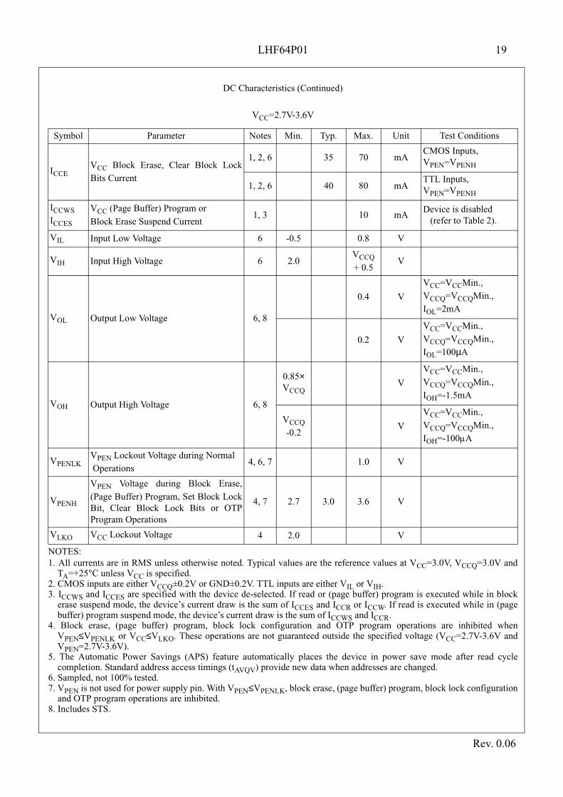
LHF64P01 19
NOTES:1. All currents are in RMS unless otherwise noted. Typical values are the reference values at VCC=3.0V, VCCQ=3.0V and
TA=+25°C unless VCC is specified.2. CMOS inputs are either VCCQ±0.2V or GND±0.2V. TTL inputs are either VIL or VIH.3. ICCWS and ICCES are specified with the device de-selected. If read or (page buffer) program is executed while in block
erase suspend mode, the device’s current draw is the sum of ICCES and ICCR or ICCW. If read is executed while in (pagebuffer) program suspend mode, the device’s current draw is the sum of ICCWS and ICCR.
4. Block erase, (page buffer) program, block lock configuration and OTP program operations are inhibited whenVPEN≤VPENLK or VCC≤VLKO. These operations are not guaranteed outside the specified voltage (VCC=2.7V-3.6V andVPEN=2.7V-3.6V).
5. The Automatic Power Savings (APS) feature automatically places the device in power save mode after read cyclecompletion. Standard address access timings (tAVQV) provide new data when addresses are changed.
6. Sampled, not 100% tested.7. VPEN is not used for power supply pin. With VPEN≤VPENLK, block erase, (page buffer) program, block lock configuration
and OTP program operations are inhibited.8. Includes STS.
ICCEVCC Block Erase, Clear Block LockBits Current
1, 2, 6 35 70 mACMOS Inputs,VPEN=VPENH
1, 2, 6 40 80 mATTL Inputs,VPEN=VPENH
ICCWS
ICCES
VCC (Page Buffer) Program orBlock Erase Suspend Current
1, 3 10 mADevice is disabled (refer to Table 2).
VIL Input Low Voltage 6 -0.5 0.8 V
VIH Input High Voltage 6 2.0VCCQ
+ 0.5V
VOL Output Low Voltage 6, 8
0.4 V
VCC=VCCMin.,VCCQ=VCCQMin.,IOL=2mA
0.2 V
VCC=VCCMin.,VCCQ=VCCQMin.,IOL=100µA
VOH Output High Voltage 6, 8
0.85×VCCQ
V
VCC=VCCMin.,VCCQ=VCCQMin.,IOH=-1.5mA
VCCQ
-0.2V
VCC=VCCMin.,VCCQ=VCCQMin.,IOH=-100µA
VPENLKVPEN Lockout Voltage during Normal Operations
4, 6, 7 1.0 V
VPENH
VPEN Voltage during Block Erase,(Page Buffer) Program, Set Block LockBit, Clear Block Lock Bits or OTPProgram Operations
4, 7 2.7 3.0 3.6 V
VLKO VCC Lockout Voltage 4 2.0 V
VCC=2.7V-3.6V
Symbol Parameter Notes Min. Typ. Max. Unit Test Conditions
Rev. 0.06
DC Characteristics (Continued)

LHF64P01 20
1.2.4 AC Characteristics - Read-Only Operations (1)
NOTES:1. Refer to AC input/output reference waveform for timing measurements and maximum allowable input slew rate.2. Sampled, not 100% tested.3. OE# may be delayed up to tELQV tGLQV after the first edge of CE0, CE1 or CE2 that enables the device
(refer to Table 2) without impact to tELQV.4. The timing is defined from the first edge of CE0, CE1 or CE2 that enables the device. 5. The timing is defined from the first edge of CE0, CE1 or CE2 that disables the device.
TA=-40°C to +85°C
VCC 3.0V-3.6V 2.7V-3.6V
VCCQ 3.0V-3.6V 2.7V-3.6V
Symbol Parameter Notes Min. Max. Min. Max. Unit
tAVAV Read Cycle Time 120 120 ns
tAVQV Address to Output Delay 120 120 ns
tELQV CEX to Output Delay 3, 4 120 120 ns
tAPA Page Address Access Time 25 30 ns
tGLQV OE# to Output Delay 3 25 30 ns
tPHQV RP# High to Output Delay 180 180 ns
tELQX CEX to Output in Low Z 2, 4 0 0 ns
tGLQX OE# to Output in Low Z 2 0 0 ns
tEHQZ CEX to Output in High Z 2, 5 35 35 ns
tGHQZ OE# to Output in High Z 2 15 15 ns
tOHOutput Hold from First Occurring Address, CEX or OE#change
2, 5 0 0 ns
tELFL/tELFH CEx Setup to BYTE# Going Low or High 2, 4 10 10 ns
tFLQV/tFHQV BYTE# to Output Delay 1000 1000 ns
tFLQZ/tFHQZ BYTE# to Output in High Z 2 1000 1000 ns
Rev. 0.06

LHF64P01 21
tAVQV
tEHQZtGHQZ
tELQV
tPHQV
tGLQV
tOH
VIH
VIL
Disabled (VIH)
Enabled (VIL)
VIH
VIL
VIH
VIL
VOH
VOL
VIH
VIL(P)
(D/Q)
(W)
(G)
(E)
(A)A22-0
DQ15-0
CEX
OE#
WE#
RP#
High Z
tELQX
VALIDOUTPUT
VALIDADDRESS
tGLQX
VIH
VIL(F)BYTE#
tAVAV
tFLQZ/tFHQZ
tFLQV/tFHQVtELFL/tELFH
Figure 6. AC Waveform for 1-Word/ 1-Byte Read Operations (Status Register, Identifier Codes, OTP Block or Query Code)
Rev. 0.06
NOTE:1. Status register, identifier codes, OTP block and query code can only be read in 1-word/ 1-byte
read operations.
LHF64P01 22
tAVQV
tELQV tEHQZtGHQZ
tOHtAPA
tGLQV
tPHQV
High Z
VIH
VIL
VIH
VIL
VOH
VOL
VIH
VIL(P)
(W)
(G)
VIH
VIL
(A)A2-1
(D/Q)DQ15-0
OE#
WE#
RP#
tGLQX
tELQX
VALIDADDRESS
VALIDADDRESS
VALIDADDRESS
VALIDOUTPUT
VALIDOUTPUT
VALIDOUTPUT
VALIDOUTPUT
VALIDADDRESS
VIH
VIL
(A)A22-3VALID
ADDRESS
Disabled (VIH)
Enabled (VIL)
(E)CEX
VIH
VIL(F)BYTE#
tFHQZ
tFHQV
tELFH
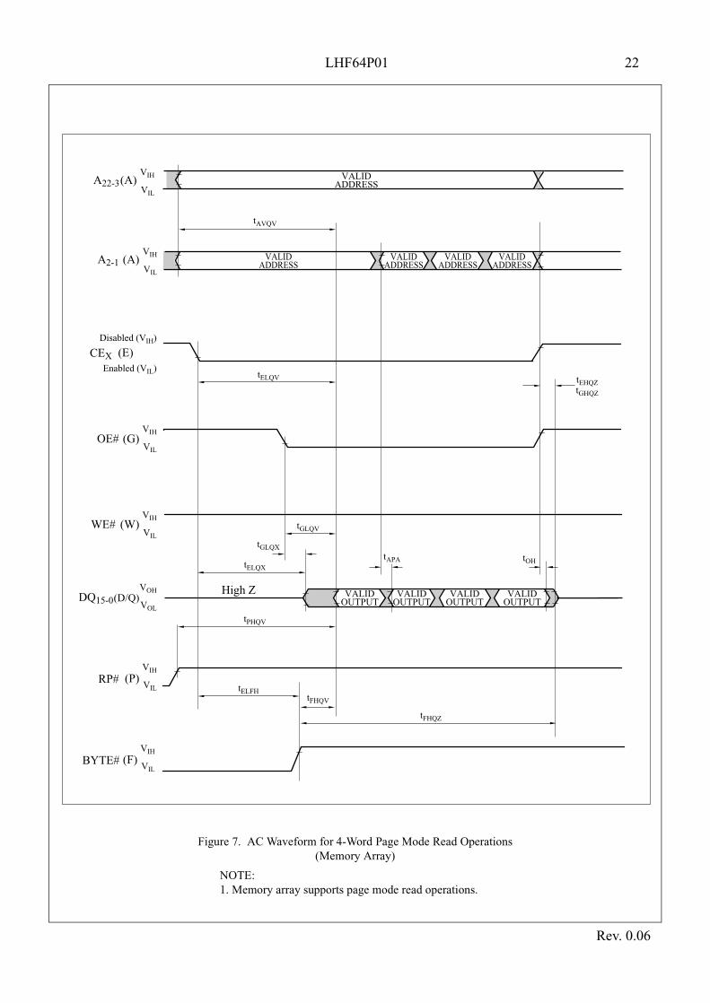
Figure 7. AC Waveform for 4-Word Page Mode Read Operations (Memory Array)
Rev. 0.06
NOTE:1. Memory array supports page mode read operations.
LHF64P01 23
Rev. 0.06
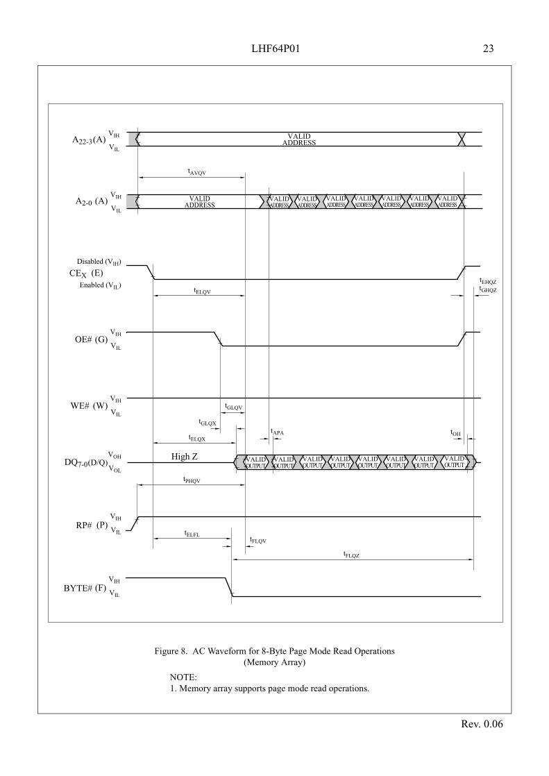
Figure 8. AC Waveform for 8-Byte Page Mode Read Operations (Memory Array)
tAVQV
tELQV
tEHQZtGHQZ
tOHtAPA
tPHQV
High Z
VIH
VIL
VIH
VIL
VOH
VOL
VIH
VIL(P)
(W)
(G)
VIH
VIL
(A)A2-0
(D/Q)DQ7-0
OE#
WE#
RP#
tGLQX
tELQX
VALIDADDRESS
VIH
VIL
(A)A22-3VALID
ADDRESS
Disabled (VIH)
Enabled (VIL)
(E)CEX
VIH
VIL(F)BYTE#
tFLQZ
tELFL
VALIDOUTPUT
VALIDOUTPUT
VALIDOUTPUT
VALIDOUTPUT
VALIDOUTPUT
VALIDOUTPUT
VALIDOUTPUT
VALIDOUTPUT
VALIDADDRESS
VALIDADDRESS
VALIDADDRESS
VALIDADDRESS
VALIDADDRESS
VALIDADDRESS
VALIDADDRESS
tFLQV
tGLQV
NOTE:1. Memory array supports page mode read operations.
LHF64P01 24
Rev. 0.06
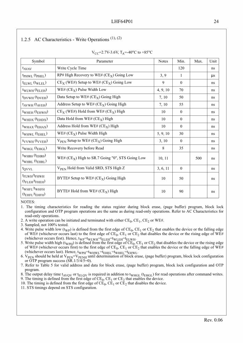
1.2.5 AC Characteristics - Write Operations (1), (2)
NOTES:1. The timing characteristics for reading the status register during block erase, (page buffer) program, block lock
configuration and OTP program operations are the same as during read-only operations. Refer to AC Characteristics forread-only operations.
2. A write operation can be initiated and terminated with either CE0, CE1, CE2 or WE#.3. Sampled, not 100% tested.4. Write pulse width low (tWP) is defined from the first edge of CE0, CE1 or CE2 that enables the device or the falling edge
of WE# (whichever occurs last) to the first edge of CE0, CE1 or CE2 that disables the device or the rising edge of WE#(whichever occurs first). Hence, tWP=tWLWH=tELEH=tWLEH=tELWH.
5. Write pulse width high (tWPH) is defined from the first edge of CE0, CE1 or CE2 that disables the device or the rising edgeof WE# (whichever occurs first) to the first edge of CE0, CE1 or CE2 that enables the device or the falling edge of WE#(whichever occurs last). Hence, tWPH=tWHWL=tEHEL=tWHEL=tEHWL.
6. VPEN should be held at VPEN=VPENH until determination of block erase, (page buffer) program, block lock configurationor OTP program success (SR.1/3/4/5=0).
7. Refer to Table 5 for valid address and data for block erase, (page buffer) program, block lock configuration and OTPprogram.
8. The output delay time tAVQV or tELQV is required in addition to tWHGL (tEHGL) for read operations after command writes.9. The timing is defined from the first edge of CE0, CE1 or CE2 that enables the device. 10. The timing is defined from the first edge of CE0, CE1 or CE2 that disables the device.11. STS timings depend on STS configuration.
VCC=2.7V-3.6V, TA=-40°C to +85°C
Symbol Parameter Notes Min. Max. Unit
tAVAV Write Cycle Time 120 ns
tPHWL (tPHEL) RP# High Recovery to WE# (CEX) Going Low 3, 9 1 µs
tELWL (tWLEL) CEX (WE#) Setup to WE# (CEX) Going Low 9 0 ns
tWLWH (tELEH) WE# (CEX) Pulse Width Low 4, 9, 10 70 ns
tDVWH (tDVEH) Data Setup to WE# (CEX) Going High 7, 10 50 ns
tAVWH (tAVEH) Address Setup to WE# (CEX) Going High 7, 10 55 ns
tWHEH (tEHWH) CEX (WE#) Hold from WE# (CEX) High 10 0 ns
tWHDX (tEHDX) Data Hold from WE# (CEX) High 10 0 ns
tWHAX (tEHAX) Address Hold from WE# (CEX) High 10 0 ns
tWHWL (tEHEL) WE# (CEX) Pulse Width High 5, 9, 10 30 ns
tVVWH (tVVEH) VPEN Setup to WE# (CEX) Going High 3, 10 0 ns
tWHGL (tEHGL) Write Recovery before Read 8 35 ns
tWHR0 (tEHR0)tWHRL (tEHRL)
WE# (CEX) High to SR.7 Going "0", STS Going Low 10, 11 500 ns
tQVVL VPEN Hold from Valid SRD, STS High Z 3, 6, 11 0 ns
tFLWH/tFHWH
(tFLEH/tFHEH)BYTE# Setup to WE# (CEX) Going High 10 50 ns
tWHFL/tWHFH
(tEHFL/tEHFH)BYTE# Hold from WE# (CEX) High 10 90 ns

LHF64P01 25
tAVAV tAVWH (tAVEH)
tWHAX(tEHAX)
tELWL (tWLEL)
tPHWL (tPHEL)
tWLWH
tWHWL (tEHEL)
tWHDX (tEHDX) tDVWH (tDVEH)
tVVWH (tVVEH)
tWHQV1,2,3,4,5,6 (tEHQV1,2,3,4,5,6)
tQVVL
tWHEH (tEHWH) tWHGL (tEHGL)
VIH
VIL
VIH
VIL
VIH
VIL
VIH
VIL
(D/Q)
(W)
(G)
(A)A22-0
DQ15-0
(V)VPEN
VIH
VPENH
VPENLK
VIL
VIL
(P)RP#
OE#
WE#
VIH
VIL(F)BYTE#
(tELEH )
VALIDADDRESS
VALIDADDRESS
VALIDADDRESS
DATA IN DATA IN VALIDSRD
("1")VOL
(R)STS
(SR.7)
High Z
("0")
(tWHR0 (tEHR0))tWHRL (tEHRL)
Disabled (VIH)
Enabled (VIL)
(E)CEX
tFLWH/tFHWH (tFLEH/tFHEH)
tWHFL/tWHFH (tEHFL/tEHFH)
NOTE 1 NOTE 2 NOTE 3
NOTE 4
NOTES 5, 6
NOTES 5, 6
NOTES:1. VCC power-up and standby.2. Write each first cycle command.3. Write each second cycle command or valid address and data.4. Automated erase or program delay. This waveform illustrates the case when STS is in level mode (RY/BY#).5. Read status register data.6. For read operation, OE# and CEX must be driven active, and WE# de-asserted.
Figure 9. AC Waveform for Write Operations
Rev. 0.06

LHF64P01 26
tPLPH
tPLPH
t2VPH
tPLRH tPHQV
tPHQV
(A) Reset during Read Array Mode
(B) Reset during Erase or Program Mode
(C) RP# rising timing
RP#
RP#
VIL
VIH
VIL
VIH
VCC
GND
VCC(min)
RP#
VIL
VIH
SR.7="1"
VOH
VOL
(D/Q)DQ15-0VALID
OUTPUTHigh Z
(P)
(P)
(P)
VOH
VOL
(D/Q)DQ15-0VALID
OUTPUTHigh Z
VOH
VOL
(D/Q)DQ15-0VALID
OUTPUTHigh Z
tPHQV
tVHQV
ABORTCOMPLETE
NOTES:1. A reset time, tPHQV, is required from the later of SR.7 (STS) going "1" (High Z) or RP# going high until outputs are valid.
Refer to AC Characteristics - Read-Only Operations for tPHQV.2. The device may reset if tPLPH is <100ns, but this is not guaranteed.3. Sampled, not 100% tested.4. If RP# asserted while a block erase, (page buffer) program, block lock configuration or OTP program operation is not
executing, the reset will complete within 100ns.5. When the device power-up, holding RP# low minimum 100ns is required after VCC has been in predefined range and also
has been in stable there.
Reset AC Specifications (VCC=2.7V-3.6V, TA=-40°C to +85°C)
Symbol Parameter Notes Min. Max. Unit
tPLPHRP# Low to Reset during Read(RP# must be low during power-up.)
1, 2, 3 100 ns
tPLRH RP# Low to Reset during Erase or Program 1, 3, 4 30 µs
t2VPH VCC 2.7V to RP# High 1, 3, 5 100 ns
tVHQV VCC 2.7V to Output Delay 3 1 ms
Figure 10. AC Waveform for Reset Operations
Rev. 0.06
1.2.6 Reset Operations

LHF64P01 27
Rev. 0.06
1.2.7 Block Erase, (Page Buffer) Program and Block Lock Configuration Performance(3)
NOTES:1. Typical values measured at VCC=3.0V, VPEN=3.0V and TA=+25°C. Assumes corresponding lock bits
are not set. Subject to change based on device characterization.2. Excludes external system-level overhead.3. Sampled, but not 100% tested.4. A latency time is required from writing suspend command (the first edge of CE0, CE1 or CE2 that disables
the device or the rising edge of WE#) until SR.7 going "1" or STS going High Z.5. If the interval time from a Block Erase Resume command to a subsequent Block Erase Suspend command is shorter
than tERES and its sequence is repeated, the block erase operation may not be finished.6. These values are valid when the page buffer is full, and the start address is aligned on a 16-word/ 32-byte boundary.7. Program time per byte (tWHQV1/ tEHQV1) is 12.5µs/byte (typical).
Program time per word (tWHQV2/ tEHQV2) is 25.0µs/word (typical).
VCC=2.7V-3.6V, TA=-40°C to +85°C
Symbol Parameter NotesVPEN=VPENH
UnitMin. Typ.(1) Max.
Page Buffer Program Time(Time to Program 16 words/ 32 bytes)
2, 6, 7
400 1200 µs
tWHQV3/tEHQV3
Program Time 2 210 630 µs
Block Program Time(Using Page Buffer Program Command)
2 1.6 4.8 s
tWHQV4/tEHQV4
Block Erase Time 2 1 5 s
tWHQV5/tEHQV5
Set Block Lock Bit Time 2 64 85 µs
tWHQV6/tEHQV6
Clear Block Lock Bits Time 2 0.5 0.7 s
tWHRH1/tEHRH1
(Page Buffer) Program SuspendLatency Time to Read
4 25 90 µs
tWHRH2/tEHRH2
Block Erase SuspendLatency Time to Read
4 26 40 µs
tERES
Latency Time from Block EraseResume Command to BlockErase Suspend Command
5 600 µs
LHF64P01 28
Rev. 0.06
2 Related Document Information(1)
NOTE:
1. International customers should contact their local SHARP or distribution sales offices.
Document No. Document Name
FUM03201 LH28F640SP series Appendix


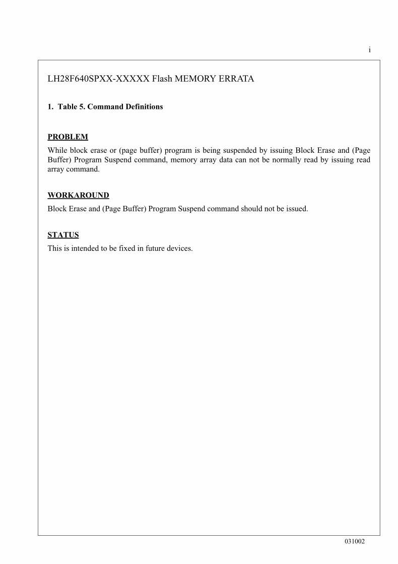
LH28F640SPXX-XXXXX Flash MEMORY ERRATA
1. Table 5. Command Definitions
PROBLEM
While block erase or (page buffer) program is being suspended by issuing Block Erase and (PageBuffer) Program Suspend command, memory array data can not be normally read by issuing readarray command.
WORKAROUND
Block Erase and (Page Buffer) Program Suspend command should not be issued.
STATUS
This is intended to be fixed in future devices.
031002
i

i
A-1 RECOMMENDED OPERATING CONDITIONS
A-1.1 At Device Power-Up
AC timing illustrated in Figure A-1 is recommended for the supply voltages and the control signals at device power-up.If the timing in the figure is ignored, the device may not operate correctly.
Figure A-1. AC Timing at Device Power-Up
For the AC specifications tVR, tR, tF in the figure, refer to the next page. See the “ELECTRICAL SPECIFICATIONS“
described in specifications for the supply voltage range, the operating temperature and the AC specifications not shown inthe next page.
t2VPHGND
VCC(min)
RP#
VIL
VIH
(P)
tPHQV
VPEN *1
GND
VPENH
(V)
WE#
VIL
VIH
(W)
OE#
VIL
VIH
(G)
VOH
VOL
(D/Q)DATA High Z Valid
Output
tVR
tF tELQV
tF tGLQV
(A)ADDRESS Valid
(RST#)
(VPP)
tR or tF
AddressVIL
VIH
tAVQVtR or tF
tR
tR
*1 To prevent the unwanted writes, system designers should consider the design, which applies VPEN (VPP)
to 0V during read operations and VPENH (VPPH) during write or erase operations.
(VPPH)
See the application note AP-007-SW-E for details.
Disabled (VIH)
Enabled (VIL)
(E)CEX
VCC
VCCQ
030313

ii
A-1.1.1 Rise and Fall Time
NOTES:1. Sampled, not 100% tested.2. This specification is applied for not only the device power-up but also the normal operations.
Symbol Parameter Notes Min. Max. Unit
tVR VCC Rise Time 1 0.5 30000 µs/V
tR Input Signal Rise Time 1, 2 1 µs/V
tF Input Signal Fall Time 1, 2 1 µs/V
030313

iii
A-1.2 Glitch Noises
Do not input the glitch noises which are below VIH (Min.) or above VIL (Max.) on address, data, reset, and control signals,
as shown in Figure A-2 (b). The acceptable glitch noises are illustrated in Figure A-2 (a).
Figure A-2. Waveform for Glitch Noises
See the “DC CHARACTERISTICS“ described in specifications for VIH (Min.) and VIL (Max.).
(a) Acceptable Glitch Noises
Input Signal
VIH (Min.)
Input Signal
VIH (Min.)
Input Signal
VIL (Max.)
Input Signal
VIL (Max.)
(b) NOT Acceptable Glitch Noises
030313
iv
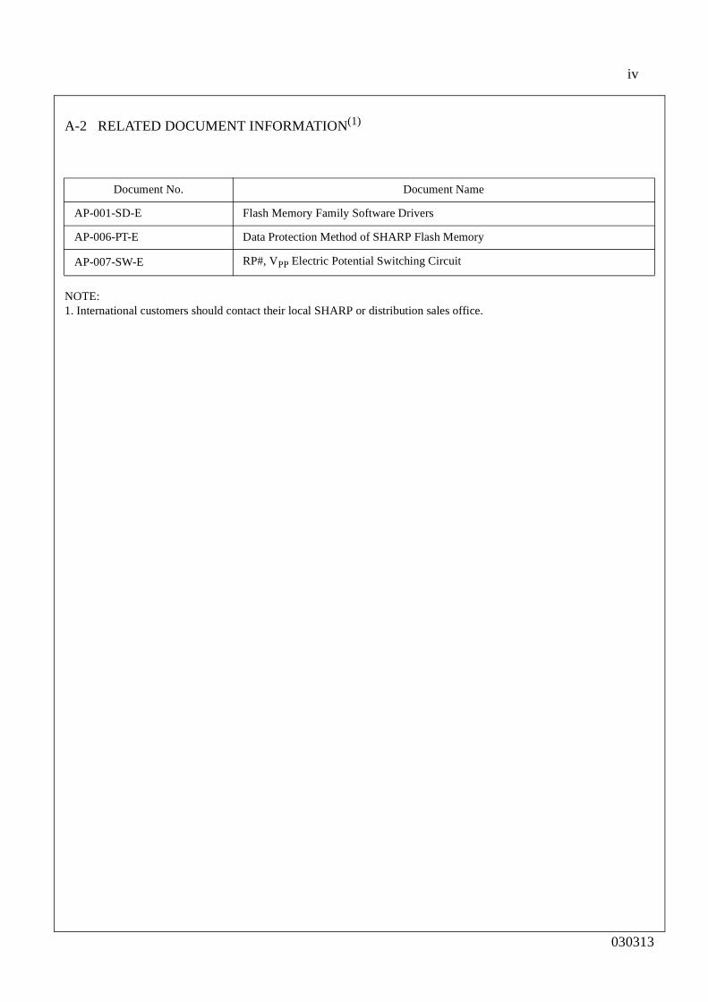
A-2 RELATED DOCUMENT INFORMATION(1)
NOTE:1. International customers should contact their local SHARP or distribution sales office.
Document No. Document Name
AP-001-SD-E Flash Memory Family Software Drivers
AP-006-PT-E Data Protection Method of SHARP Flash Memory
AP-007-SW-E RP#, VPP Electric Potential Switching Circuit
030313