
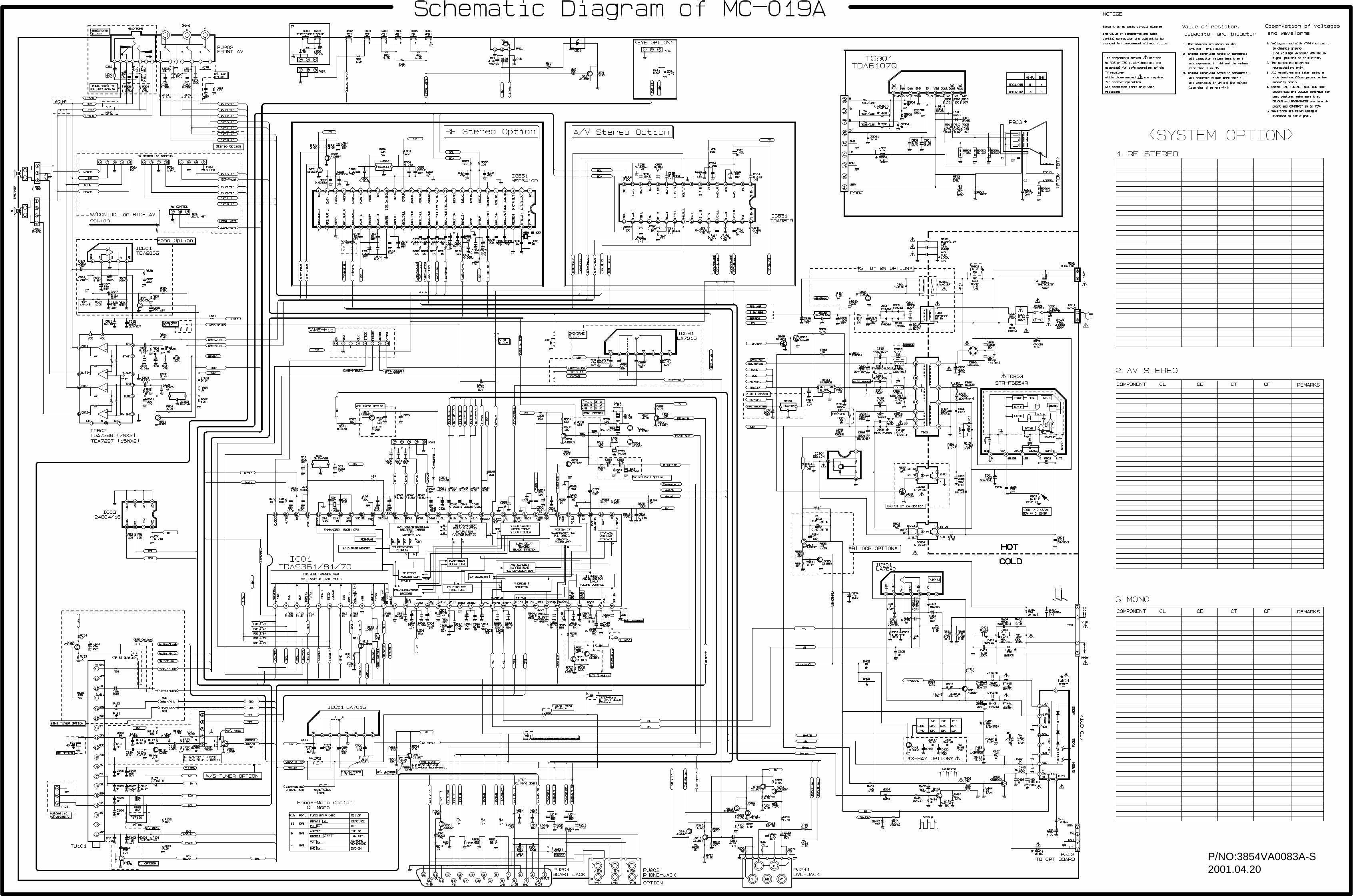
Lg Chassis Mc019a 188
14
- 11 - O Safety Precautions 1. It is safe to adjust after using insulating transformer between the power supply line and chassis input to prevent the risk of electric shock and protect the instrument. 2. Never disconnect leads while the TV receiver is on. 3. Don't short any portion of circuits while power is on. 4. The adjustment must be done by the correct appliances. But this is changeable in view of productivity. 5. Unless otherwise noted, set the line voltage to 110~240Vac !10%, 50/60Hz. 6. The adjustment of TV should be performed afther warming up for 20 minutes. O Test Equipment required 1. Multimeter (volt meter) 2. Oscilloscope 3. 10:1 PROBE 4. Color Analyzer O CDL Data Adjustment(LINE SVC-0) 1) Press the SVC button to get into the SVC-0 Mode. 2) Press the Channel UP/DOWN button to select CDL12. 3) Press the Volume UP/DOWN button until the CDL data is the same as the Table below. 4) Press the OK(V) button to memorize the data. O OPTION Data Adjustment(OPTION-1,OPTION-2) 1) Press OK buttons on both TV set and Remote Controller at the same time to get into SVC mode. 2) Press the Yellow button several times to find OPTION-1 or OPTION-2. 3) Input the correspond OPTION data referring to Table below with the numeric buttons. 4) Press the OK(V) button to memorize the data. Table 1. OPTION 1 Function Table 2. OPTION 2 Function Table 3. OPTION 3 Function ADJUSTMENT 21” FCD 12 FLAT 14,16” CPT 8 15” CPT 10 FLAT 20,21” CPT 12 CDL Data Remark 0 1 0 1 0 1 0 1 0 1 SCART TOP 2 IN 1 DVD C MUTE Option Code Function Remark ACTIVE NOT ACTIVE W/O DVD DVD(REAR JACK) W/O 2 IN 1TUNER WITH 2 IN 1TUNER FLOF TXT TOP TXT PHONO JACK SCART JACK 0 1 0 1 0 1 0 1 EYE TBS MONO 4 KEY Option Code Function Remark W/O TBS WITH TBS W/O EYE WITH EYE W/O 4 KEY WITH 4 KEY FORCED MONO 0 1 0 1 0 1 0 1 0 1 0 1 0 1 0 1 0 1 ACMS T-SCH T-P/S CURVE DUAL CHA + AU 200 PRO GAME BCF Option Code Function Remark Auto Abnormal ON Not Used W/O GAME PACK WITH GAME PACK 100 PRO 200 PRO Except China,Austrailia China,Austrailia W/O DUAL WITH DUAL Austrailia Except Austrailia W/O TURBO SEARCH WITH TURBO SEARCH W/O TURBO P/S WITH TURBO P/S NORMAL VOLUME CURVE M-A,India VOLUME CURVE 0 1 0 1 0 1 2 3 4 5 6 7 SYSTEM HOTEL RESER VED Option Code Function Remark * * * * * * W/O HOTEL W/HOTEL BG/L BG/I/DK BG/I/DK/M BG/I/DK DUAL BG/I/DK/M DUAL 2nd IF BG 2nd IF I 2nd IF DK
Transcript of Lg Chassis Mc019a 188
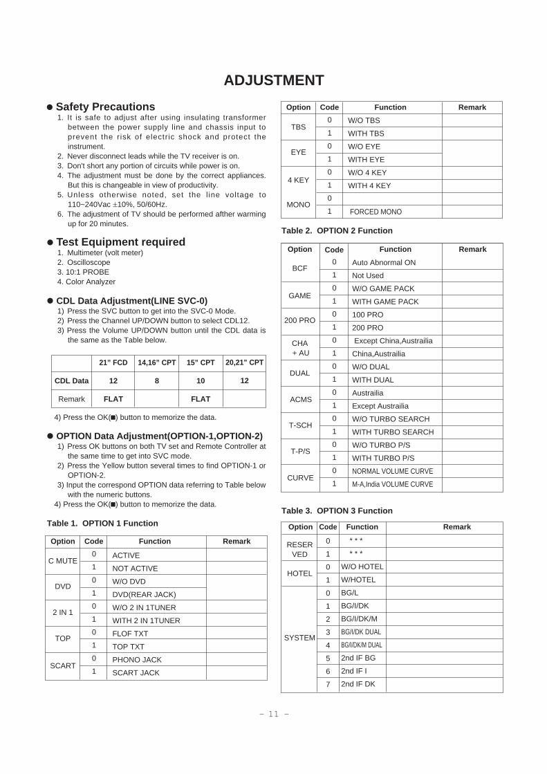
- 11 -
O Safety Precautions1. It is safe to adjust after using insulating transformer
between the power supply line and chassis input toprevent the risk of electric shock and protect theinstrument.
2. Never disconnect leads while the TV receiver is on.3. Don't short any portion of circuits while power is on.4. The adjustment must be done by the correct appliances.
But this is changeable in view of productivity.5. Unless otherwise noted, set the l ine voltage to
110~240Vac !10%, 50/60Hz.6. The adjustment of TV should be performed afther warming
up for 20 minutes.
O Test Equipment required1. Multimeter (volt meter)2. Oscilloscope3. 10:1 PROBE4. Color Analyzer
O CDL Data Adjustment(LINE SVC-0)1) Press the SVC button to get into the SVC-0 Mode.2) Press the Channel UP/DOWN button to select CDL12. 3) Press the Volume UP/DOWN button until the CDL data is
the same as the Table below.
4) Press the OK(V) button to memorize the data.
O OPTION Data Adjustment(OPTION-1,OPTION-2)1) Press OK buttons on both TV set and Remote Controller at
the same time to get into SVC mode.2) Press the Yellow button several times to find OPTION-1 or
OPTION-2.3) Input the correspond OPTION data referring to Table below
with the numeric buttons.4) Press the OK(V) button to memorize the data.
Table 1. OPTION 1 Function
Table 2. OPTION 2 Function
Table 3. OPTION 3 Function
ADJUSTMENT
21” FCD
12
FLAT
14,16” CPT
8
15” CPT
10
FLAT
20,21” CPT
12CDL Data
Remark
0
1
0
1
0
1
0
1
0
1SCART
TOP
2 IN 1
DVD
C MUTE
Option Code Function Remark
ACTIVE
NOT ACTIVE
W/O DVD
DVD(REAR JACK)
W/O 2 IN 1TUNER
WITH 2 IN 1TUNER
FLOF TXT
TOP TXT
PHONO JACK
SCART JACK
0
1
0
1
0
1
0
1
EYE
TBS
MONO
4 KEY
Option Code Function Remark
W/O TBS
WITH TBS
W/O EYE
WITH EYE
W/O 4 KEY
WITH 4 KEY
FORCED MONO
0
1
0
1
0
1
0
1
0
1
0
1
0
1
0
1
0
1
ACMS
T-SCH
T-P/S
CURVE
DUAL
CHA+ AU
200 PRO
GAME
BCF
Option Code Function Remark
Auto Abnormal ON
Not Used
W/O GAME PACK
WITH GAME PACK
100 PRO
200 PRO
Except China,Austrailia
China,Austrailia
W/O DUAL
WITH DUAL
Austrailia
Except Austrailia
W/O TURBO SEARCH
WITH TURBO SEARCH
W/O TURBO P/S
WITH TURBO P/S
NORMAL VOLUME CURVE
M-A,India VOLUME CURVE
0
1
0
1
0
1
2
3
4
5
6
7
SYSTEM
HOTEL
RESERVED
Option Code Function Remark
* * *
* * *
W/O HOTEL
W/HOTEL
BG/L
BG/I/DK
BG/I/DK/M
BG/I/DK DUAL
BG/I/DK/M DUAL
2nd IF BG
2nd IF I
2nd IF DK
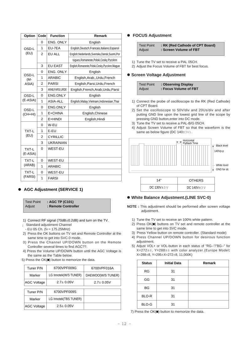
- 12 -
O AGC Adjustment (SERVICE 1)
1) Connect RF signal (70dB!0.2dB) and turn on the TV.¡ Standard adjustment Channel
- EU 05 Ch. (frf = 175.25MHz) 2) Press the OK buttons on TV set and Remote Controller at the
same time to get into SVC-0 mode.3) Press the Channel UP/DOWN button on the Remote
Controller several times to find AGC??.4) Press the Volume UP/DOWN button until the AGC Voltage is
the same as the Table below.5) Press the OK(V) button to memorize the data.
O FOCUS Adjustment
1) Tune the TV set to receive a PAL 05CH.2) Adjust the Focus Volume of FBT for best focus.
O Screen Voltage Adjustment
1) Connect the probe of oscilloscope to the RK (Red Cathode)of CPT Board.
2) Set the oscilloscope to 50V/div and 20Us/div and afterputting GND line upon the lowest grid line of the scope bypressing GND button,enter into DC mode.
3) Tune the TV set to receive a PAL-B/G 05CH.4) Adjust Screen Volume of FBT so that the waveform is the
same as below figure (DC 140!3V).
O White Balance Adjustment.(LINE SVC-0)
NOTE : This adjustment should be performed after screen voltageadjustment.
1) Tune the TV set to receive an 100% white pattern.2) Press OK(V) buttons on TV set and remote controller at the
same time to get into SVC mode.3) Press Yellow button on remote controller. (Standard mode)4) Press Channel UP/DOWN button for desirous function
adjustment.5) Adjust VOL+ or VOL-button in each status of "RG--"/"BG--" for
X=272!8, Y=288!8 with color analyzer.(Europe Model:X=288!8, Y=295!X=272!8, 11,000K)
7) Press the OK(V) button to memorize the data.
Test Point : AGC TP (C101) Adjust : Remote Controller
Tuner P/N
Marker
AGC Voltage
6700VPF009G
LG Innotek(W/S TUNER)
2.7! 0.05V
6700VPF016A
DAEWOO(W/S TUNER)
2.7! 0.05V
Tuner P/N
Marker
AGC Voltage
6700VPF009S
LG Innotek(TBS TUNER)
2.5! 0.05V
Test Point : Observing DisplayAdjust : Focus Volume of FBT
Test Point : RK (Red Cathode of CPT Board)Adjust : Screen Volume of FBT
HorizontalFlyBack Time
Black level
White level
GND for dc
140Vp-p
Status
RG
GG
BG
BLO-R
BLO-G
Initial Data
31
31
31
31
31
Remark
0
1
2
3
0
1
2
3
0
1
0
1
2
0
1
2
3
0
0
1
0
1
OSD-L(E-ASIA)
OSD-L(CH+HI)
English
English,Deutsch,Francais,Italiano,Espanol
English,Nederlands,Svenska,Dansk,Suomi,Por
tugues,Romaneste,Polski,Cesky,Pyccknn
English,Romaneste,Polski,Cesky,Pyccknn,Magyar
English
English,Arab,,Urdu,French
English,Parsi,Urdu,French
English,French,Arab,Urdu,Parsi
English
English,Malay,Vietnam,Indonesian,Thai
English
English,Chinese
English,Hindi
TXT-L(EU)
TXT-L(E-ASIA)
TXT-L(ARAB)
TXT-L(FARSI)
OSD-L(EU)
OSD-L(M-
ASIA)
Option Code Function Remark
ENG. ONLY
EU-7EA
EU ALL
EU EAST
ENG. ONLY
ARABIC
PARSI
ARAB,FARSI,URDE
ENG.ONLY
ASIA-ALL
ENG.ONLY
E+CHINA
E+HINDI
W-EU
E-EU
CYRILLIC
UKRAINIAN
WEST-EU
WEST-EU
ARABIC
WEST-EU
FARSI14”
DC 130V!3V
OTHERS
DC 140V!3V
- 13 -
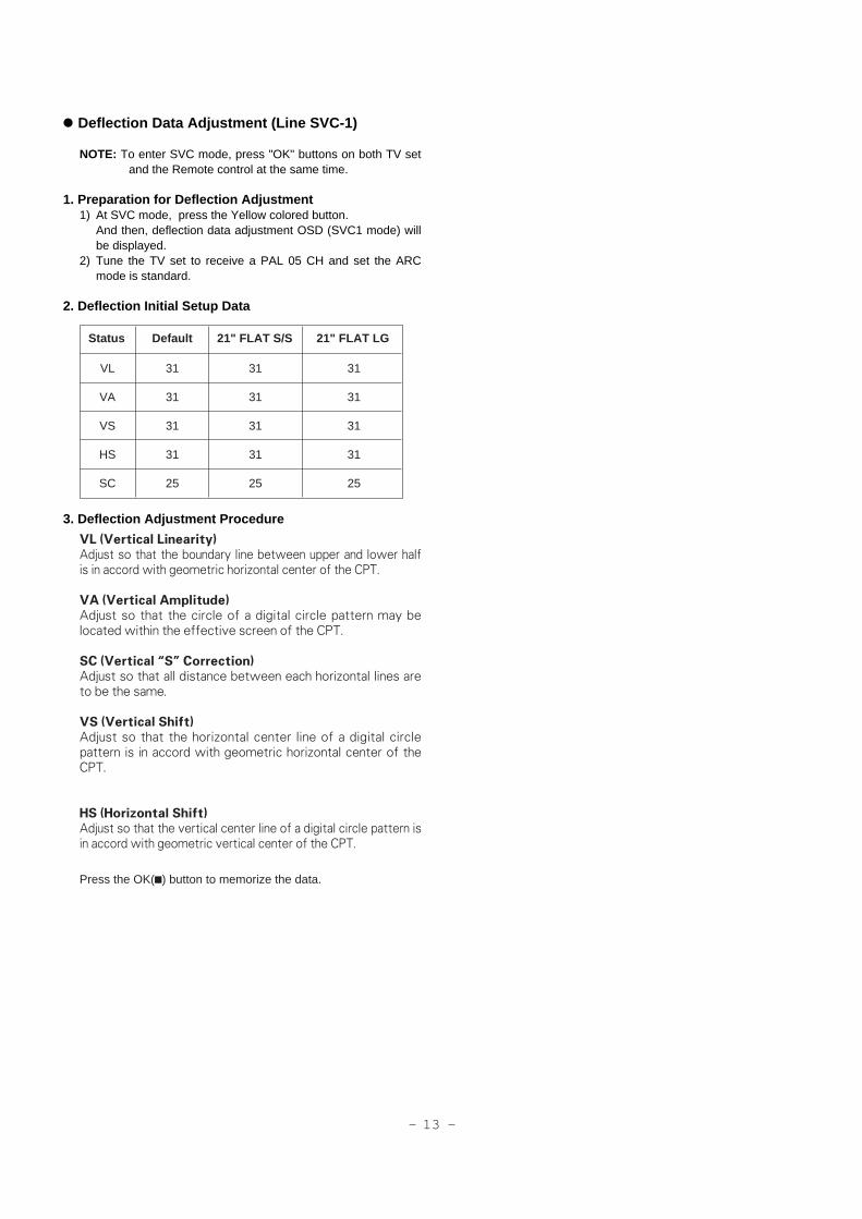
O Deflection Data Adjustment (Line SVC-1)
NOTE: To enter SVC mode, press "OK" buttons on both TV setand the Remote control at the same time.
1. Preparation for Deflection Adjustment 1) At SVC mode, press the Yellow colored button.
And then, deflection data adjustment OSD (SVC1 mode) willbe displayed.
2) Tune the TV set to receive a PAL 05 CH and set the ARCmode is standard.
2. Deflection Initial Setup Data
3. Deflection Adjustment Procedure
VL (Vertical Linearity)Adjust so that the boundary line between upper and lower halfis in accord with geometric horizontal center of the CPT.
VA (Vertical Amplitude)Adjust so that the circle of a digital circle pattern may belocated within the effective screen of the CPT.
SC (Vertical “S” Correction)Adjust so that all distance between each horizontal lines areto be the same.
VS (Vertical Shift)Adjust so that the horizontal center line of a digital circlepattern is in accord with geometric horizontal center of theCPT.
HS (Horizontal Shift)Adjust so that the vertical center line of a digital circle pattern isin accord with geometric vertical center of the CPT.
Press the OK(V) button to memorize the data.
VL
VA
VS
HS
SC
31
31
31
31
25
31
31
31
31
25
31
31
31
31
25
Status Default 21" FLAT S/S 21" FLAT LG
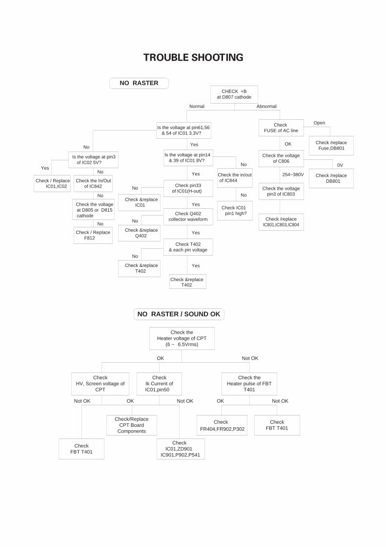
NO RASTERCHECK +B
at D807 cathode
Is the voltage at pin14 & 39 of IC01 8V?
Check FUSE of AC line
Check the voltageof C806
Check the voltagepin3 of IC803
Check pin33of IC01(H-out)
Check Q402collector waveform
Check T402& each pin voltage
Check &replace T402
Check &replaceIC01
Check &replaceQ402
Check &replaceT402
Check the in/outof IC844
Check IC01pin1 high?
Check /replaceIC801,IC803,IC804
Check /replaceFuse,DB801
Check /replaceDB801
Normal Abnormal
Yes
Yes
Yes
Yes
No
No
No
No
NoNo
No
No
No
OK
254~380V
Open
0V
Is the voltage at pin61,56 & 54 of IC01 3.3V?
Yes
Is the voltage at pin3 of IC02 5V?
Check the In/Outof IC842
Check the voltageat D805 or D815 cathode
Check / ReplaceF812
Check / ReplaceIC01,IC02
Yes
NO RASTER / SOUND OK
Check theHeater voltage of CPT
(6 ~ 6.5Vrms)
CheckFR404,FR902,P302
CheckFBT T401
Check theHeater pulse of FBT
T401
CheckIk Current ofIC01,pin50
Not OK
OK Not OK
Check/ReplaceCPT Board
Components
CheckIC01,ZD901
IC901,P902,P541
OK Not OK
OK
CheckHV, Screen voltage of
CPT
CheckFBT T401
Not OK
TROUBLE SHOOTING
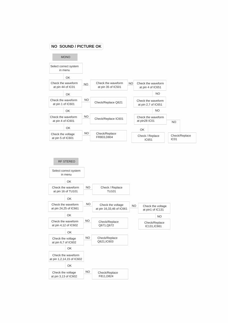
NO SOUND / PICTURE OK
Select correct system in menu
Check the waveform at pin 35 of IC501
Check the waveform at pin 4 of IC651
Check the waveform at pin 44 of IC01
Check the waveform at pin 4 of IC601
Check the voltage at pin 5 of IC601
Check the waveform at pin 1 of IC601 Check/Replace Q621
Check/Replace FR803,D804
Check/Replace IC601
OK
OK
OK
Check the waveform at pin 2,7 of IC651
OK
NO
NOCheck / Replace
IC651Check/Replace IC01
Check the waveformat pin28 IC01
NO
NO
MONO
Select correct system in menu
Check / ReplaceTU101
Check the voltage at pin 16,33,46 of IC661
NO
OK
Check the waveform at pin 16 of TU101
Check the waveform at pin 4,12 of IC602
Check the voltage at pin 6,7 of IC602
Check the waveformat pin 1,2,14,15 of IC602
Check the voltage at pin 3,13 of IC602
Check the waveform at pin 24,25 of IC661
Check/Replace F811,D824
Check/Replace Q621,IC603
Check/ReplaceQ671,Q672
OK
OK
OK
OK
OK
NO
NO
Check the voltageat pin1 of IC131
RF STEREO
NO
NO
NO
NO
NO
NO
NO
NO
OK
Check/Replace IC131,IC661
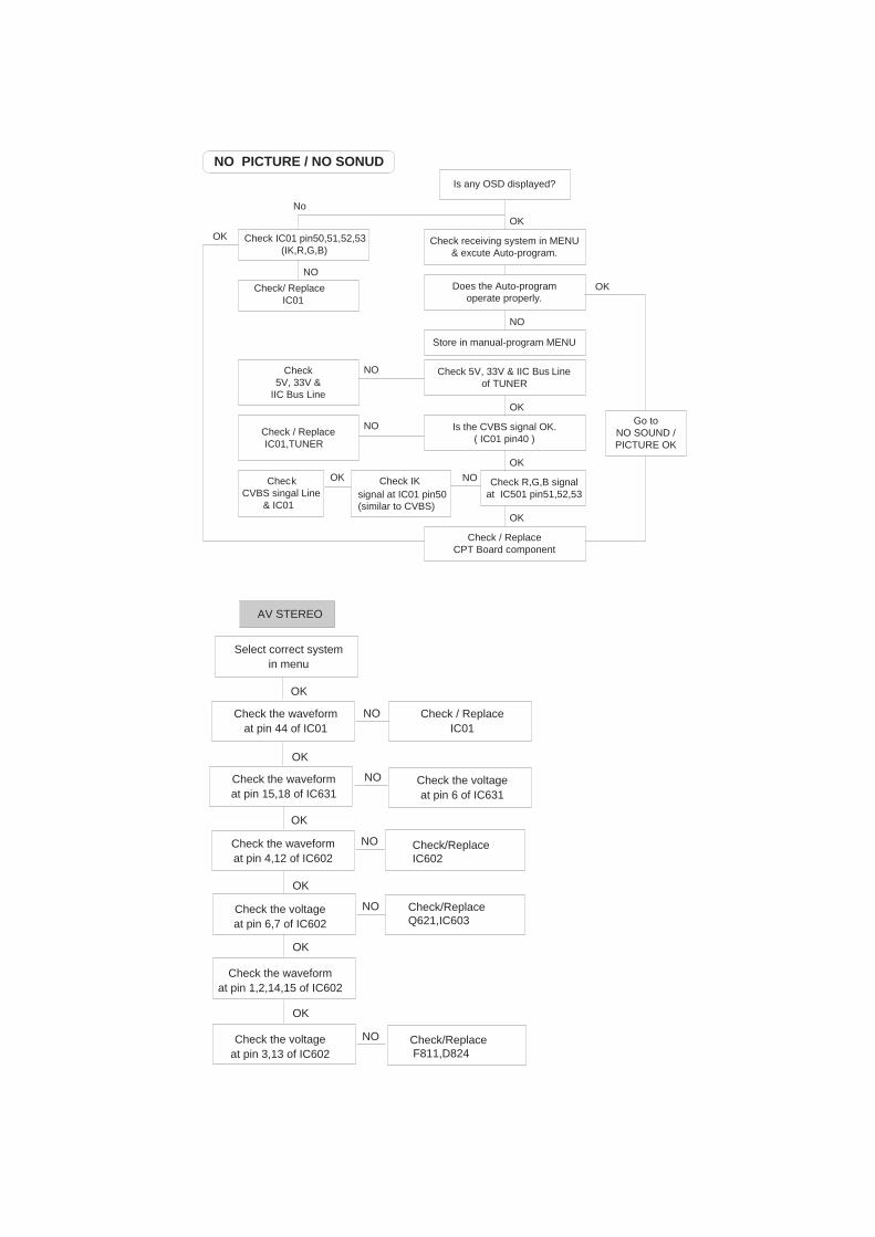
NO PICTURE / NO SONUD
Is any OSD displayed?
Check receiving system in MENU& excute Auto-program.
OK
OK
NO
Check/ ReplaceIC01
No
Go toNO SOUND /PICTURE OK
Does the Auto-programoperate properly.
Store in manual-program MENU
Check 5V, 33V & IIC Bus Lineof TUNER
Is the CVBS signal OK.( IC01 pin40 )
Check R,G,B signalat IC501 pin51,52,53
Check5V, 33V &
IIC Bus Line
OK
NO
NO
OK
OK
Check / ReplaceIC01,TUNER
NO
OK
Check / ReplaceCPT Board component
CheckCVBS singal Line
& IC01
Check IK signal at IC01 pin50(similar to CVBS)
Check IC01 pin50,51,52,53(IK,R,G,B)
OK
NO
Select correct system in menu
Check / ReplaceIC01
Check the voltage at pin 6 of IC631
NO
OK
Check the waveform at pin 44 of IC01
Check the waveform at pin 4,12 of IC602
Check the voltage at pin 6,7 of IC602
Check the waveformat pin 1,2,14,15 of IC602
Check the voltage at pin 3,13 of IC602
Check the waveform at pin 15,18 of IC631
Check/Replace F811,D824
Check/Replace Q621,IC603
Check/ReplaceIC602
OK
OK
OK
OK
OK
NO
NO
AV STEREO
NO
NO
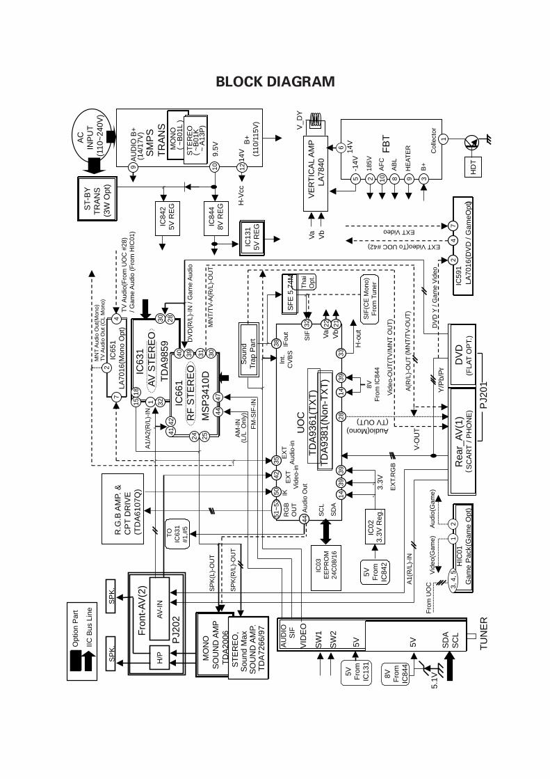
BLOCK DIAGRAM
DV
D(F
LAT
OP
T.)
R.G
.B A
MP.
&
CP
T D
RIV
E(T
DA
6107
Q)
FB
T
185V
-14V
AF
C
AB
L
HE
AT
ER
B+
HD
T
Col
lect
or
A1(
R/L
)-IN
SP
K(R
/L)-
OU
T
UO
CT
DA
9361
(TX
T)
H/P
AV
-IN
AU
DIO
B+
B+
(110
/115
V)
(14/
17V
)S
MP
S
TR
AN
S
SP
K.
Fro
nt-A
V(2
)
(MN
T/T
V-O
UT
)
14V
H-o
ut
IFou
tIn
t.C
VB
S
SC
L
SD
A
EX
TV
ideo
-in
RG
BO
UT
IK
H-V
cc
VID
EO
TU
NE
R
V_D
Y
VE
RT
ICA
L A
MP
LA78
40V
a
Rea
r_A
V(1
)S
CA
RT
/ P
HO
NE
)(
IC03
EE
PR
OM
24C
08/1
6
A(R
/L)-
OU
TV
-OU
T
EX
T.R
GB
Vb
Va
Vb
SP
K.
9.5V
5V Fro
mIC
131
A1/
A2(
R/L
)-IN
Y/P
b/P
r
DV
D(R
/L)-
IN /
Gam
e A
udio
MN
T/T
V-A
(R/L
)-O
UT
SIF
FM
-SIF
-IN
SW
1
SW
2
SD
AS
CL
MS
P34
10DTD
A98
59A
V S
TE
RE
O
RF
ST
ER
EO
M
ON
OS
OU
ND
AM
P T
DA
2006
AC
IN
PU
T(1
10~
240V
)
ST
ER
EO
,S
ound
Max
SO
UN
D A
MP.
TD
A72
66/9
7
ST
ER
EO
,S
ound
Max
SO
UN
D A
MP.
TD
A72
66/9
7
IC
131
5V R
EG
Opt
ion
Par
t
IIC B
us L
ine
TD
A93
81(N
on-T
XT
)
Audio(Mono)(TVOUT)28
332122
38
S
ound
Trap
Par
t
Vid
eo-O
UT
(TV
/MN
T O
UT
)
5042
51~
53
°‹
°‹
°‹
°‹°‹
ST
ER
EO
( ~
B01
K ~
A13
P)
MO
NO
(
~B
01L
)
10 129
5 398102
6 14V
1
ST-
BY
T
RA
NS
(3
W O
pt) °‹
SP
K(L
)-O
UT
°‹
24 25
4744
AU
DIO
A
M-I
N(L
/L O
nly)
3039 31402830
1439
8VF
rom
IC84
4
1439
39
3.3V
Reg
.
5V Fro
mIC
842
3.3V
°‹°‹
8V Fro
mIC
844
IC
844
8V R
EG
IC
842
5V R
EG
4142
1 32
IC02
IC63
1
IC66
1
5V 5V
5.1V
SF
E 5
.74M
32S
IF
SIF
(CE
Mon
o)F
rom
Tun
er
°‹
35E
XT
Aud
io-in
°‹
IC
651
LA70
16(M
ono
Opt
)
7
2
TV
Aud
io(F
rom
UO
C #
28)
/ Gam
e A
udio
(F
rom
HIC
01)
4
MN
T A
udio
Out
(Mon
o)T
V A
udio
Out
(C
L M
ono)
°‹
°‹
LA
7016
(DV
D /
Gam
eOpt
) IC
591
)
2
DV
D Y
/ G
ame
Vid
eo
47EXTVideo
PJ2
01
EXTVideo(ToUOC#42)
H
IC01
Gam
e P
ack(
Gam
e O
pt)
3, 4
, 51
2
Fro
m U
OC
Vid
eo(G
ame)
Aud
io(G
ame)
PJ2
02
1518
44A
udio
Out
T
OIC
631
#1,#
5
Tha
iO
pt.
°‹
P/NO:3854VA0083A-S2001.04.20
- 18 -
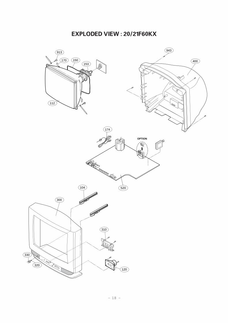
EXPLODED VIEW : 20/21F60KX
310
104
300
330
320120
943
400
913
170 150153
112
174
520
OPTION
- 19 -
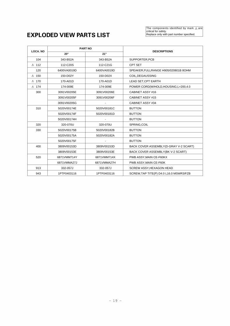
104 343-B52A 343-B52A SUPPORTER,PCB
112 112-C20S 112-C21G CPT SET
120 6400VA0019D 6400VA0019D SPEAKER,FULLRANGE H905/020801B 8OHM
150 150-D02Y 150-D02X COIL,DEGAUSSING
170 170-A01D 170-A01D LEAD SET,CPT EARTH
174 174-009E 174-009E POWER CORD(W/HOLD,HOUSING,L=200,4.0
300 3091V00205E 3091V00206E CABINET ASSY #16
3091V00205F 3091V00206F CABINET ASSY #15
3091V00205G - CABINET ASSY #34
310 5020V00174E 5020V00181C BUTTON
5020V00174F 5020V00181D BUTTON
5020V00174H - BUTTON
320 320-070U 320-070U SPRING,COIL
330 5020V00175B 5020V00182B BUTTON
5020V00175A 5020V00182A BUTTON
5020V00175F - BUTTON
400 3809V00153D 3809V00153D BACK COVER ASSEMBLY(D-GRAY V-2 SCART)
3809V00153E 3809V00153E BACK COVER ASSEMBLY(BK V-2 SCART)
520 6871VMM714Y 6871VMM714X PWB ASSY,MAIN CE-F60KX
6871VMMA27J 6871VMMA27H PWB ASSY,MAIN CE-F60K
913 332-057J 332-057J SCREW ASSY,HEXAGON HEAD
943 1PTF0403116 1PTF0403116 SCREW,TAP TITE(P) D4.0 L16.0 MSWR3/FZB
EXPLODED VIEW PARTS LISTThe components identified by mark arecritical for safety.Replace only with part number specified.
LOCA. NO DESCRIPTIONSPART NO
20" 21"
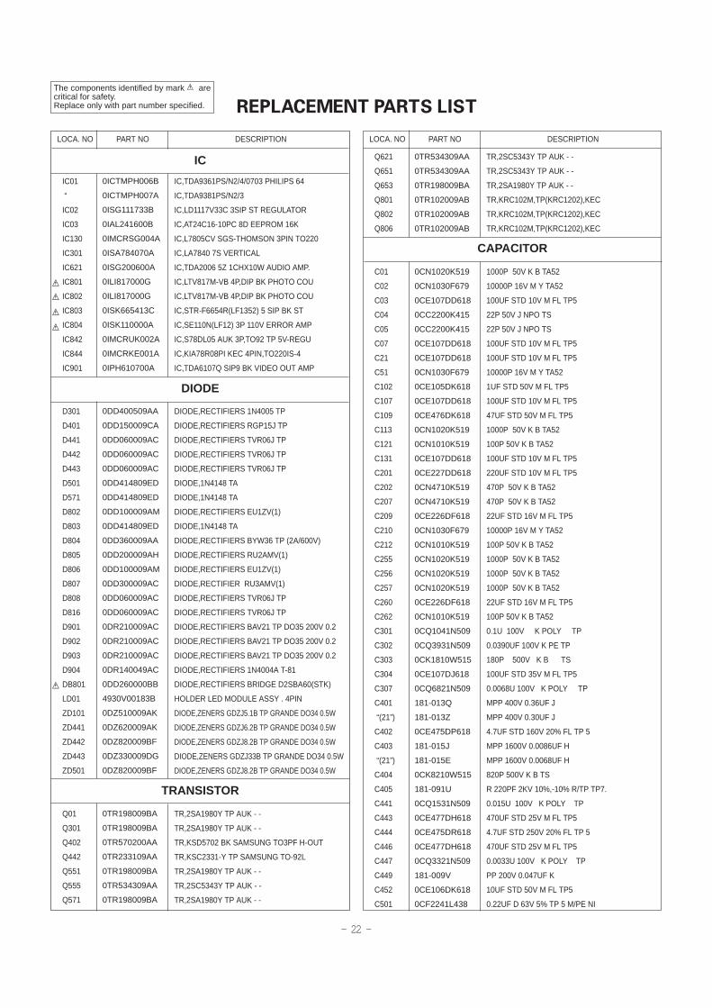
REPLACEMENT PARTS LIST
LOCA. NO PART NO DESCRIPTION
IC01
“
IC02
IC03
IC130
IC301
IC621
IC801
IC802
IC803
IC804
IC842
IC844
IC901
D301
D401
D441
D442
D443
D501
D571
D802
D803
D804
D805
D806
D807
D808
D816
D901
D902
D903
D904
DB801
LD01
ZD101
ZD441
ZD442
ZD443
ZD501
Q01
Q301
Q402
Q442
Q551
Q555
Q571
0ICTMPH006B
0ICTMPH007A
0ISG111733B
0IAL241600B
0IMCRSG004A
0ISA784070A
0ISG200600A
0ILI817000G
0ILI817000G
0ISK665413C
0ISK110000A
0IMCRUK002A
0IMCRKE001A
0IPH610700A
0DD400509AA
0DD150009CA
0DD060009AC
0DD060009AC
0DD060009AC
0DD414809ED
0DD414809ED
0DD100009AM
0DD414809ED
0DD360009AA
0DD200009AH
0DD100009AM
0DD300009AC
0DD060009AC
0DD060009AC
0DR210009AC
0DR210009AC
0DR210009AC
0DR140049AC
0DD260000BB
4930V00183B
0DZ510009AK
0DZ620009AK
0DZ820009BF
0DZ330009DG
0DZ820009BF
0TR198009BA
0TR198009BA
0TR570200AA
0TR233109AA
0TR198009BA
0TR534309AA
0TR198009BA
IC,TDA9361PS/N2/4/0703 PHILIPS 64
IC,TDA9381PS/N2/3
IC,LD1117V33C 3SIP ST REGULATOR
IC,AT24C16-10PC 8D EEPROM 16K
IC,L7805CV SGS-THOMSON 3PIN TO220
IC,LA7840 7S VERTICAL
IC,TDA2006 5Z 1CHX10W AUDIO AMP.
IC,LTV817M-VB 4P,DIP BK PHOTO COU
IC,LTV817M-VB 4P,DIP BK PHOTO COU
IC,STR-F6654R(LF1352) 5 SIP BK ST
IC,SE110N(LF12) 3P 110V ERROR AMP
IC,S78DL05 AUK 3P,TO92 TP 5V-REGU
IC,KIA78R08PI KEC 4PIN,TO220IS-4
IC,TDA6107Q SIP9 BK VIDEO OUT AMP
DIODE,RECTIFIERS 1N4005 TP
DIODE,RECTIFIERS RGP15J TP
DIODE,RECTIFIERS TVR06J TP
DIODE,RECTIFIERS TVR06J TP
DIODE,RECTIFIERS TVR06J TP
DIODE,1N4148 TA
DIODE,1N4148 TA
DIODE,RECTIFIERS EU1ZV(1)
DIODE,1N4148 TA
DIODE,RECTIFIERS BYW36 TP (2A/600V)
DIODE,RECTIFIERS RU2AMV(1)
DIODE,RECTIFIERS EU1ZV(1)
DIODE,RECTIFIER RU3AMV(1)
DIODE,RECTIFIERS TVR06J TP
DIODE,RECTIFIERS TVR06J TP
DIODE,RECTIFIERS BAV21 TP DO35 200V 0.2
DIODE,RECTIFIERS BAV21 TP DO35 200V 0.2
DIODE,RECTIFIERS BAV21 TP DO35 200V 0.2
DIODE,RECTIFIERS 1N4004A T-81
DIODE,RECTIFIERS BRIDGE D2SBA60(STK)
HOLDER LED MODULE ASSY . 4PIN
DIODE,ZENERS GDZJ5.1B TP GRANDE DO34 0.5W
DIODE,ZENERS GDZJ6.2B TP GRANDE DO34 0.5W
DIODE,ZENERS GDZJ8.2B TP GRANDE DO34 0.5W
DIODE,ZENERS GDZJ33B TP GRANDE DO34 0.5W
DIODE,ZENERS GDZJ8.2B TP GRANDE DO34 0.5W
TR,2SA1980Y TP AUK - -
TR,2SA1980Y TP AUK - -
TR,KSD5702 BK SAMSUNG TO3PF H-OUT
TR,KSC2331-Y TP SAMSUNG TO-92L
TR,2SA1980Y TP AUK - -
TR,2SC5343Y TP AUK - -
TR,2SA1980Y TP AUK - -
LOCA. NO PART NO DESCRIPTION
Q621
Q651
Q653
Q801
Q802
Q806
C01
C02
C03
C04
C05
C07
C21
C51
C102
C107
C109
C113
C121
C131
C201
C202
C207
C209
C210
C212
C255
C256
C257
C260
C262
C301
C302
C303
C304
C307
C401
“(21”)
C402
C403
“(21”)
C404
C405
C441
C443
C444
C446
C447
C449
C452
C501
0TR534309AA
0TR534309AA
0TR198009BA
0TR102009AB
0TR102009AB
0TR102009AB
0CN1020K519
0CN1030F679
0CE107DD618
0CC2200K415
0CC2200K415
0CE107DD618
0CE107DD618
0CN1030F679
0CE105DK618
0CE107DD618
0CE476DK618
0CN1020K519
0CN1010K519
0CE107DD618
0CE227DD618
0CN4710K519
0CN4710K519
0CE226DF618
0CN1030F679
0CN1010K519
0CN1020K519
0CN1020K519
0CN1020K519
0CE226DF618
0CN1010K519
0CQ1041N509
0CQ3931N509
0CK1810W515
0CE107DJ618
0CQ6821N509
181-013Q
181-013Z
0CE475DP618
181-015J
181-015E
0CK8210W515
181-091U
0CQ1531N509
0CE477DH618
0CE475DR618
0CE477DH618
0CQ3321N509
181-009V
0CE106DK618
0CF2241L438
TR,2SC5343Y TP AUK - -
TR,2SC5343Y TP AUK - -
TR,2SA1980Y TP AUK - -
TR,KRC102M,TP(KRC1202),KEC
TR,KRC102M,TP(KRC1202),KEC
TR,KRC102M,TP(KRC1202),KEC
1000P 50V K B TA52
10000P 16V M Y TA52
100UF STD 10V M FL TP5
22P 50V J NPO TS
22P 50V J NPO TS
100UF STD 10V M FL TP5
100UF STD 10V M FL TP5
10000P 16V M Y TA52
1UF STD 50V M FL TP5
100UF STD 10V M FL TP5
47UF STD 50V M FL TP5
1000P 50V K B TA52
100P 50V K B TA52
100UF STD 10V M FL TP5
220UF STD 10V M FL TP5
470P 50V K B TA52
470P 50V K B TA52
22UF STD 16V M FL TP5
10000P 16V M Y TA52
100P 50V K B TA52
1000P 50V K B TA52
1000P 50V K B TA52
1000P 50V K B TA52
22UF STD 16V M FL TP5
100P 50V K B TA52
0.1U 100V K POLY TP
0.0390UF 100V K PE TP
180P 500V K B TS
100UF STD 35V M FL TP5
0.0068U 100V K POLY TP
MPP 400V 0.36UF J
MPP 400V 0.30UF J
4.7UF STD 160V 20% FL TP 5
MPP 1600V 0.0086UF H
MPP 1600V 0.0068UF H
820P 500V K B TS
R 220PF 2KV 10%,-10% R/TP TP7.
0.015U 100V K POLY TP
470UF STD 25V M FL TP5
4.7UF STD 250V 20% FL TP 5
470UF STD 25V M FL TP5
0.0033U 100V K POLY TP
PP 200V 0.047UF K
10UF STD 50V M FL TP5
0.22UF D 63V 5% TP 5 M/PE NI
IC
DIODE
CAPACITOR
- 22 -
The components identified by mark arecritical for safety.Replace only with part number specified.
TRANSISTOR
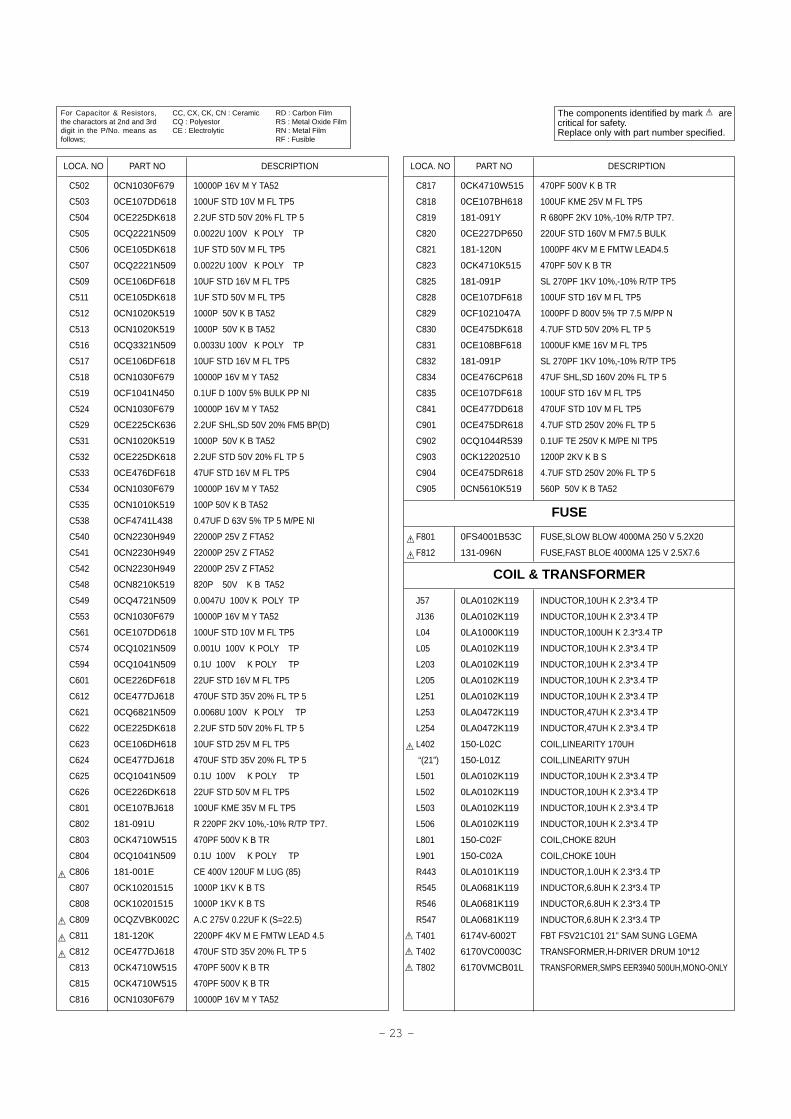
- 23 -
LOCA. NO PART NO DESCRIPTION
C502
C503
C504
C505
C506
C507
C509
C511
C512
C513
C516
C517
C518
C519
C524
C529
C531
C532
C533
C534
C535
C538
C540
C541
C542
C548
C549
C553
C561
C574
C594
C601
C612
C621
C622
C623
C624
C625
C626
C801
C802
C803
C804
C806
C807
C808
C809
C811
C812
C813
C815
C816
0CN1030F679
0CE107DD618
0CE225DK618
0CQ2221N509
0CE105DK618
0CQ2221N509
0CE106DF618
0CE105DK618
0CN1020K519
0CN1020K519
0CQ3321N509
0CE106DF618
0CN1030F679
0CF1041N450
0CN1030F679
0CE225CK636
0CN1020K519
0CE225DK618
0CE476DF618
0CN1030F679
0CN1010K519
0CF4741L438
0CN2230H949
0CN2230H949
0CN2230H949
0CN8210K519
0CQ4721N509
0CN1030F679
0CE107DD618
0CQ1021N509
0CQ1041N509
0CE226DF618
0CE477DJ618
0CQ6821N509
0CE225DK618
0CE106DH618
0CE477DJ618
0CQ1041N509
0CE226DK618
0CE107BJ618
181-091U
0CK4710W515
0CQ1041N509
181-001E
0CK10201515
0CK10201515
0CQZVBK002C
181-120K
0CE477DJ618
0CK4710W515
0CK4710W515
0CN1030F679
10000P 16V M Y TA52
100UF STD 10V M FL TP5
2.2UF STD 50V 20% FL TP 5
0.0022U 100V K POLY TP
1UF STD 50V M FL TP5
0.0022U 100V K POLY TP
10UF STD 16V M FL TP5
1UF STD 50V M FL TP5
1000P 50V K B TA52
1000P 50V K B TA52
0.0033U 100V K POLY TP
10UF STD 16V M FL TP5
10000P 16V M Y TA52
0.1UF D 100V 5% BULK PP NI
10000P 16V M Y TA52
2.2UF SHL,SD 50V 20% FM5 BP(D)
1000P 50V K B TA52
2.2UF STD 50V 20% FL TP 5
47UF STD 16V M FL TP5
10000P 16V M Y TA52
100P 50V K B TA52
0.47UF D 63V 5% TP 5 M/PE NI
22000P 25V Z FTA52
22000P 25V Z FTA52
22000P 25V Z FTA52
820P 50V K B TA52
0.0047U 100V K POLY TP
10000P 16V M Y TA52
100UF STD 10V M FL TP5
0.001U 100V K POLY TP
0.1U 100V K POLY TP
22UF STD 16V M FL TP5
470UF STD 35V 20% FL TP 5
0.0068U 100V K POLY TP
2.2UF STD 50V 20% FL TP 5
10UF STD 25V M FL TP5
470UF STD 35V 20% FL TP 5
0.1U 100V K POLY TP
22UF STD 50V M FL TP5
100UF KME 35V M FL TP5
R 220PF 2KV 10%,-10% R/TP TP7.
470PF 500V K B TR
0.1U 100V K POLY TP
CE 400V 120UF M LUG (85)
1000P 1KV K B TS
1000P 1KV K B TS
A.C 275V 0.22UF K (S=22.5)
2200PF 4KV M E FMTW LEAD 4.5
470UF STD 35V 20% FL TP 5
470PF 500V K B TR
470PF 500V K B TR
10000P 16V M Y TA52
LOCA. NO PART NO DESCRIPTION
C817
C818
C819
C820
C821
C823
C825
C828
C829
C830
C831
C832
C834
C835
C841
C901
C902
C903
C904
C905
F801
F812
J57
J136
L04
L05
L203
L205
L251
L253
L254
L402
“(21”)
L501
L502
L503
L506
L801
L901
R443
R545
R546
R547
T401
T402
T802
0CK4710W515
0CE107BH618
181-091Y
0CE227DP650
181-120N
0CK4710K515
181-091P
0CE107DF618
0CF1021047A
0CE475DK618
0CE108BF618
181-091P
0CE476CP618
0CE107DF618
0CE477DD618
0CE475DR618
0CQ1044R539
0CK12202510
0CE475DR618
0CN5610K519
0FS4001B53C
131-096N
0LA0102K119
0LA0102K119
0LA1000K119
0LA0102K119
0LA0102K119
0LA0102K119
0LA0102K119
0LA0472K119
0LA0472K119
150-L02C
150-L01Z
0LA0102K119
0LA0102K119
0LA0102K119
0LA0102K119
150-C02F
150-C02A
0LA0101K119
0LA0681K119
0LA0681K119
0LA0681K119
6174V-6002T
6170VC0003C
6170VMCB01L
470PF 500V K B TR
100UF KME 25V M FL TP5
R 680PF 2KV 10%,-10% R/TP TP7.
220UF STD 160V M FM7.5 BULK
1000PF 4KV M E FMTW LEAD4.5
470PF 50V K B TR
SL 270PF 1KV 10%,-10% R/TP TP5
100UF STD 16V M FL TP5
1000PF D 800V 5% TP 7.5 M/PP N
4.7UF STD 50V 20% FL TP 5
1000UF KME 16V M FL TP5
SL 270PF 1KV 10%,-10% R/TP TP5
47UF SHL,SD 160V 20% FL TP 5
100UF STD 16V M FL TP5
470UF STD 10V M FL TP5
4.7UF STD 250V 20% FL TP 5
0.1UF TE 250V K M/PE NI TP5
1200P 2KV K B S
4.7UF STD 250V 20% FL TP 5
560P 50V K B TA52
FUSE,SLOW BLOW 4000MA 250 V 5.2X20
FUSE,FAST BLOE 4000MA 125 V 2.5X7.6
INDUCTOR,10UH K 2.3*3.4 TP
INDUCTOR,10UH K 2.3*3.4 TP
INDUCTOR,100UH K 2.3*3.4 TP
INDUCTOR,10UH K 2.3*3.4 TP
INDUCTOR,10UH K 2.3*3.4 TP
INDUCTOR,10UH K 2.3*3.4 TP
INDUCTOR,10UH K 2.3*3.4 TP
INDUCTOR,47UH K 2.3*3.4 TP
INDUCTOR,47UH K 2.3*3.4 TP
COIL,LINEARITY 170UH
COIL,LINEARITY 97UH
INDUCTOR,10UH K 2.3*3.4 TP
INDUCTOR,10UH K 2.3*3.4 TP
INDUCTOR,10UH K 2.3*3.4 TP
INDUCTOR,10UH K 2.3*3.4 TP
COIL,CHOKE 82UH
COIL,CHOKE 10UH
INDUCTOR,1.0UH K 2.3*3.4 TP
INDUCTOR,6.8UH K 2.3*3.4 TP
INDUCTOR,6.8UH K 2.3*3.4 TP
INDUCTOR,6.8UH K 2.3*3.4 TP
FBT FSV21C101 21” SAM SUNG LGEMA
TRANSFORMER,H-DRIVER DRUM 10*12
TRANSFORMER,SMPS EER3940 500UH,MONO-ONLY
For Capacitor & Resistors,the charactors at 2nd and 3rddigit in the P/No. means asfollows;
CC, CX, CK, CN : CeramicCQ : PolyestorCE : Electrolytic
RD : Carbon FilmRS : Metal Oxide FilmRN : Metal FilmRF : Fusible
The components identified by mark arecritical for safety.Replace only with part number specified.
FUSE
COIL & TRANSFORMER
- 24 -
LOCA. NO PART NO DESCRIPTION
P301
P802
P902
P903
C546
D813
FR441
FR442
“(21”)
FR443
FR802
FR803
J30
J33
J39
J69
J101
J154
L01
L10
L210
R01
R03
R04
R05
R06
R07
R09
R10
R13
R14
R16
R18
R21
R22
R23
R25
R26
R27
R29
R51
R52
R105
R106
R107
R201
R204
R205
366-043K
366-043B
387-603E
366-009D
0RD1103F609
0RS0272H609
0RF0470J607
0RF0101J607
0RF0121K607
0RF0470J607
0RF0470H609
0RF0470K607
0RD2200F609
0RD2200F609
0RD2200F609
0RD1000F609
0RD2002F609
0RD1101F609
0RD1500F609
0RD0102F609
0RD0101F609
0RD1002F609
0RD1000F609
0RD3301F609
0RD3301F609
0RD4701F609
0RD4701F609
0RD1000F609
0RD1000F609
0RD1000F609
0RD1603F609
0RD4701F609
0RD1203F609
0RD2201F609
0RD3902F609
0RD2200F609
0RD1201F609
0RD1601F609
0RD3601F609
0RD1201F609
0RD1000F609
0RD1000F609
0RD1000F609
0RD1000F609
0RS0272J607
0RD0682F609
0RD0752F609
0RD0822F609
CONNECTOR (CIRC),PLUG(4P)
CONNECTOR (CIRC)ASSY,PLUG(2P)
CONNECTOR ASSY,9PIN (IL-J)
CONNECTOR (CIRC),2.36PAI 1P
110K OHM 1/6 W 5.00% TA52
27 OHM 1/2 W 5.00% TA52
0.47 OHM 1 W 5.00% TA62
1 OHM 1 W 5.00% TA62
1.2 OHM 2 W 5.00% TA62
0.47 OHM 1 W 5.00% TA62
0.47 OHM 1/2 W 5.00% TA52
0.47 OHM 2 W 5.00% TA62
220 OHM 1/6 W 5.00% TA52
220 OHM 1/6 W 5.00% TA52
220 OHM 1/6 W 5.00% TA52
100 OHM 1/6 W 5.00% TA52
20K OHM 1/6 W 5.00% TA52
1.1K OHM 1/6 W 5.00% TA52
150 OHM 1/6 W 5.00% TA52
10 OHM 1/6 W 5.00% TA52
1 OHM 1/6 W 5.00% TA52
10K OHM 1/6 W 5.00% TA52
100 OHM 1/6 W 5.00% TA52
3.3K OHM 1/6 W 5.00% TA52
3.3K OHM 1/6 W 5.00% TA52
4.7K OHM 1/6 W 5.00% TA52
4.7K OHM 1/6 W 5.00% TA52
100 OHM 1/6 W 5.00% TA52
100 OHM 1/6 W 5.00% TA52
100 OHM 1/6 W 5.00% TA52
160K OHM 1/6 W 5.00% TA52
4.7K OHM 1/6 W 5.00% TA52
120K OHM 1/6 W 5.00% TA52
2.2K OHM 1/6 W 5.00% TA52
39K OHM 1/6 W 5.00% TA52
220 OHM 1/6 W 5.00% TA52
1.2K OHM 1/6 W 5.00% TA52
1.6K OHM 1/6 W 5.00% TA52
3.6K OHM 1/6 W 5.00% TA52
1.2K OHM 1/6 W 5.00% TA52
100 OHM 1/6 W 5.00% TA52
100 OHM 1/6 W 5.00% TA52
100 OHM 1/6 W 5.00% TA52
100 OHM 1/6 W 5.00% TA52
27 OHM 1 W 5.00% TA62
68 OHM 1/6 W 5.00% TA52
75 OHM 1/6 W 5.00% TA52
82 OHM 1/6 W 5.00% TA52
LOCA. NO PART NO DESCRIPTION
R206
R207
R208
R251
R254
R255
R301
R302
“(21”)
R304
R305
R306
R307
“(21”)
R310
R311
R312
R313
R401
R402
R442
R444
R446
R447
“(21”)
R450
R451
R453
“(21”)
R455
R456
“(21”)
R501
R502
R504
R506
R518
R521
R522
R523
R524
R537
R538
R539
R540
R542
R544
R551
R552
R558
R559
R572
0RD0822F609
0RD0822F609
0RD1001F609
0RD0822F609
0RD2200H609
0RD2200H609
0RD0101F609
0RN1201F409
0RN1501F409
0RD0221H609
0RD0221H609
0RS2700K607
0RD1201F609
0RD1501F609
0RD1801F609
0RD4701H609
0RD2201F609
0RD1002F609
0RD1501H609
0RS2702K607
0RD5100H609
0RD0392H609
0RD1001F609
0RD3301F609
0RD3901F609
0RD4701H609
0RD1200H609
0RS3302H609
0RS4702H609
0RS2702K607
0RS5102H609
0RS2702H609
0RD2202F609
0RD1002F609
0RN3902F409
0RD1001F609
0RD3302F609
0RD1000F609
0RD2702F609
0RD1003F609
0RD3001F609
0RD1000F609
0RD1000F609
0RD1000F609
0RD1000F609
0RD1002F609
0RD2701F609
0RD3300F609
0RD3300F609
0RD4701F609
0RD1800F609
0RD5600F609
82 OHM 1/6 W 5.00% TA52
82 OHM 1/6 W 5.00% TA52
1K OHM 1/6 W 5.00% TA52
82 OHM 1/6 W 5.00% TA52
220 OHM 1/2 W 5.00% TA52
220 OHM 1/2 W 5.00% TA52
1 OHM 1/6 W 5.00% TA52
1.2K OHM 1/6 W 1.00% TA52
1.5K OHM 1/6 W 1.00% TA52
2.2 OHM 1/2 W 5.00% TA52
2.2 OHM 1/2 W 5.00% TA52
270 OHM 2 W 5.00% TA62
1.2K OHM 1/6 W 5.00% TA52
1.5K OHM 1/6 W 5.00% TA52
1.8K OHM 1/6 W 5.00% TA52
4.7K OHM 1/2 W 5.00% TA52
2.2K OHM 1/6 W 5.00% TA52
10K OHM 1/6 W 5.00% TA52
1.5K OHM 1/2 W 5.00% TA52
27K OHM 2 W 5.00% TA62
510 OHM 1/2 W 5.00% TA52
39 OHM 1/2 W 5.00% TA52
1K OHM 1/6 W 5.00% TA52
3.3K OHM 1/6 W 5.00% TA52
3.9K OHM 1/6 W 5.00% TA52
4.7K OHM 1/2 W 5.00% TA52
120 OHM 1/2 W 5.00% TA52
33K OHM 1/2 W 5.00% TA52
47K OHM 1/2 W 5.00% TA52
27K OHM 2 W 5.00% TA62
51K OHM 1/2 W 5.00% TA52
27K OHM 1/2 W 5.00% TA52
22K OHM 1/6 W 5.00% TA52
10K OHM 1/6 W 5.00% TA52
39K OHM 1/6 W 1.00% TA52
1K OHM 1/6 W 5.00% TA52
33K OHM 1/6 W 5.00% TA52
100 OHM 1/6 W 5.00% TA52
27K OHM 1/6 W 5.00% TA52
100K OHM 1/6 W 5.00% TA52
3K OHM 1/6 W 5.00% TA52
100 OHM 1/6 W 5.00% TA52
100 OHM 1/6 W 5.00% TA52
100 OHM 1/6 W 5.00% TA52
100 OHM 1/6 W 5.00% TA52
10K OHM 1/6 W 5.00% TA52
2.7K OHM 1/6 W 5.00% TA52
330 OHM 1/6 W 5.00% TA52
330 OHM 1/6 W 5.00% TA52
4.7K OHM 1/6 W 5.00% TA52
180 OHM 1/6 W 5.00% TA52
560 OHM 1/6 W 5.00% TA52
The components identified by mark arecritical for safety.Replace only with part number specified.
For Capacitor & Resistors,the charactors at 2nd and 3rddigit in the P/No. means asfollows;
CC, CX, CK, CN : CeramicCQ : PolyestorCE : Electrolytic
RD : Carbon FilmRS : Metal Oxide FilmRN : Metal FilmRF : Fusible
RESISTOR
CONNECTOR
- 25 -
LOCA. NO PART NO DESCRIPTION
R573
R621
R622
R623
R624
R625
R626
R627
R628
R651
R652
R657
R660
R801
R802
R803
R804
R805
R806
R808
R809
R812
R813
R814
R815
R816
R903
R904
R905
R906
R907
R908
R909
R910
R911
R912
RC801
SW01
SW02
SW03
SW04
SW05
SW06
SW801
FB801
FB802
FB803
L201
0RD2403F609
0RD9102F609
0RD6801F609
0RD1003F609
0RD1003F609
0RD1003F609
0RD5101F609
0RD3301F609
0RD0331H609
0RD4700F609
0RD2200F609
0RD4300F609
0RD4702F609
0RD2701F609
0RD2201F609
0RD1001F609
0RD4701F609
180-A01M
0RD2401F609
0RD4701F609
0RS4702K607
0RK8204H609
0RD1002F609
0RD0221H609
0RD0751H609
0RD2001F609
0RD2200F609
0RD2200F609
0RD2200F609
0RD1000F609
0RD1000F609
0RD1000F609
0RS1501H609
0RS1501H609
0RS1501H609
0RD2204H609
180-822N
140-315A
140-315A
140-315A
140-315A
140-315A
140-315A
6600VM2002A
125-022R
125-022R
125-022R
125-022R
240K OHM 1/6 W 5.00% TA52
91K OHM 1/6 W 5.00% TA52
6.8K OHM 1/6 W 5.00% TA52
100K OHM 1/6 W 5.00% TA52
100K OHM 1/6 W 5.00% TA52
100K OHM 1/6 W 5.00% TA52
5.1K OHM 1/6 W 5.00% TA52
3.3K OHM 1/6 W 5.00% TA52
3.3 OHM 1/2 W 5.00% TA52
470 OHM 1/6 W 5.00% TA52
220 OHM 1/6 W 5.00% TA52
430 OHM 1/6 W 5.00% TA52
47K OHM 1/6 W 5.00% TA52
2.7K OHM 1/6 W 5.00% TA52
2.2K OHM 1/6 W 5.00% TA52
1K OHM 1/6 W 5.00% TA52
4.7K OHM 1/6 W 5.00% TA52
0.22 OHM 2 W 5% TA62 RW ROUND
2.4K OHM 1/6 W 5.00% TA52
4.7K OHM 1/6 W 5.00% TA52
47K OHM 2 W 5.00% TA62
8.2M OHM 1/2 W 5.00% TA52
10K OHM 1/6 W 5.00% TA52
2.2 OHM 1/2 W 5.00% TA52
7.5 OHM 1/2 W 5.00% TA52
2K OHM 1/6 W 5.00% TA52
220 OHM 1/6 W 5.00% TA52
220 OHM 1/6 W 5.00% TA52
220 OHM 1/6 W 5.00% TA52
100 OHM 1/6 W 5.00% TA52
100 OHM 1/6 W 5.00% TA52
100 OHM 1/6 W 5.00% TA52
1.5K OHM 1/2 W 5.00% TA52
1.5K OHM 1/2 W 5.00% TA52
1.5K OHM 1/2 W 5.00% TA52
2.2M OHM 1/2 W 5.00% TA52
RWR 7W 1.0 OHM J PD
SWITCH,TACT SKHV17910B LG C&D NON 12V
SWITCH,TACT SKHV17910B LG C&D NON 12V
SWITCH,TACT SKHV17910B LG C&D NON 12V
SWITCH,TACT SKHV17910B LG C&D NON 12V
SWITCH,TACT SKHV17910B LG C&D NON 12V
SWITCH,TACT SKHV17910B LG C&D NON 12V
SWITCH,SDKEA3 ALPS IEC 250V 8A HORIZO
FILTER,EMC BI3857 FEELUX 5.7X3.6MM
FILTER,EMC BI3857 FEELUX 5.7X3.6MM
FILTER,EMC BI3857 FEELUX 5.7X3.6MM
FILTER,EMC BI3857 FEELUX 5.7X3.6MM
LOCA. NO PART NO DESCRIPTION
L255
L260
T801
X01
A1
A2
A2
A3
PA01
PJ201
PJ202
SK901
TH801
TU101
VD801
125-123A
125-022R
150-F06W
156-A02B
3828VA0271N
6710V00070A
6710V00070B
5010V00004B
6726VV0006H
381-091A
6613V00006C
6620VBC003A
163-054F
6700VPF009Q
164-003G
FILTER,EMC FERRITE BFD3565R2F(TAPING)
FILTER,EMC BI3857 FEELUX 5.7X3.6MM
FILTER,EMC SQE2930 36MH 0.5PHY 105TURN
RESONATOR,CRYSTAL HC49U 12.000MHZ 30P
MANUAL,OWNERS MC019A NON LG RO
REMOTE CONTROLLER MC-019A,W/ TXT.34KEY .
REMOTE CONTROLLER MC-019A,W/OTXT
ANTENNA 2 POLE 3 SECTION 700MM 750MM N
REMOTE CONTROLLER RECEIVER 38KHZ
SOCKET,S-091A 21PIN H
JACK ASSY,PJ6062C 2P<YL(SW)WH(SW)>+
SOCKET,CPT PCS030A 8PIN 14/360
THERMISTOR,J502P84D140M290Q
TUNER,TAFL-M232D MULTI FS 2IN1 3S
VARISTOR,TVR621D14A 620V 10% U
The components identified by mark arecritical for safety.Replace only with part number specified.
For Capacitor & Resistors,the charactors at 2nd and 3rddigit in the P/No. means asfollows;
CC, CX, CK, CN : CeramicCQ : PolyestorCE : Electrolytic
RD : Carbon FilmRS : Metal Oxide FilmRN : Metal FilmRF : Fusible
ACCESSORIES
MISCELLANEOUS
SWITCH
FILTER & CRYSTAL