Lessons from Nanoelectronics A.Basic Concepts
272
November 20, 2016 20:5 ws-book9x6 Lessons from Nanoelectronics: A. Basic Concepts ws-book9x6 page i Half-title page, prepared by publisher i Lessons from Nanoelectronics A. Basic Concepts Supriyo Datta Purdue University World Scientific (2012) Second Edition, 2017 Manuscript, not FINAL
Transcript of Lessons from Nanoelectronics A.Basic Concepts

November 20, 2016 20:5 ws-book9x6 Lessons from Nanoelectronics: A. Basic Concepts ws-book9x6 page i
Half-title page, prepared by publisher
i
Lessons from NanoelectronicsA. Basic Concepts
Supriyo DattaPurdue University
World Scientific (2012) Second Edition, 2017
Manuscript, not FINAL

February 27, 2017 19:5 ws-book9x6 Lessons from Nanoelectronics: A. Basic Concepts 10440-main page v
To Malika, Manoshi
and Anuradha
v

February 27, 2017 19:5 ws-book9x6 Lessons from Nanoelectronics: A. Basic Concepts 10440-main page vi

February 27, 2017 19:5 ws-book9x6 Lessons from Nanoelectronics: A. Basic Concepts 10440-main page vii
Preface
Everyone is familiar with the amazing performance of a modern smart-
phone, powered by a billion-plus nanotransistors, each having an active
region that is barely a few hundred atoms long. I believe we also owe a ma-
jor intellectual debt to the many who have made this technology possible.
This is because the same amazing technology has also led to a deeper un-
derstanding of the nature of current flow and heat dissipation on an atomic
scale which I believe should be of broad relevance to the general problems
of non-equilibrium statistical mechanics that pervade many different fields.
To make these lectures accessible to anyone in any branch of science or
engineering, we assume very little background beyond linear algebra and
differential equations. However, we will be discussing advanced concepts
that should be of interest even to specialists, who are encouraged to look
at my earlier books for additional technical details.
This book is based on a set of two online courses originally offered in 2012
on nanoHUB-U and more recently in 2015 on edX. In preparing the second
edition we decided to split it into parts A and B entitled Basic Concepts
and Quantum Transport respectively, along the lines of the two courses.
A list of available video lectures corresponding to different sections of this
volume is provided upfront. I believe readers will find these useful.
Even this Second Edition represents lecture notes in unfinished form. I plan
to keep posting additions/corrections at the companion website.
vii

February 27, 2017 19:5 ws-book9x6 Lessons from Nanoelectronics: A. Basic Concepts 10440-main page viii

February 27, 2017 19:5 ws-book9x6 Lessons from Nanoelectronics: A. Basic Concepts 10440-main page ix
Acknowledgments
The precursor to this lecture note series, namely the Electronics from the
Bottom Up initiative on www.nanohub.org was funded by the U.S. National
Science Foundation (NSF), the Intel Foundation, and Purdue University.
Thanks to World Scientific Publishing Corporation and, in particular, our
series editor, Zvi Ruder for joining us in this partnership.
In 2012 nanoHUB-U offered its first two online courses based on this text.
We gratefully acknowledge Purdue and NSF support for this program, along
with the superb team of professionals who made nanoHUB-U a reality
(https://nanohub.org/u) and later helped offer these courses through edX.
A special note of thanks to Mark Lundstrom for his leadership that made
it all happen and for his encouragement and advice. I am grateful to Shu-
vro Chowdhury for carefully going through this new edition and fixing the
many errors introduced during conversion to LATEX. I also owe a lot to
many students, ex-students, on-line students and colleagues for their valu-
able feedback and suggestions regarding these lecture notes.
Finally I would like to express my deep gratitude to all who have helped
me learn, a list that includes many teachers, colleagues and students over
the years, starting with the late Richard Feynman whose classic lectures on
physics, I am sure, have inspired many like me and taught us the “pleasure
of finding things out.”
Supriyo Datta
ix

February 27, 2017 19:5 ws-book9x6 Lessons from Nanoelectronics: A. Basic Concepts 10440-main page x
February 27, 2017 19:5 ws-book9x6 Lessons from Nanoelectronics: A. Basic Concepts 10440-main page xi
List of Available Video Lectures
This book is based on a set of two online courses originally offered in 2012 on
nanoHUB-U and more recently in 2015 on edX. These courses are now avail-
able in self-paced format at nanoHUB-U (https://nanohub.org/u) along
with many other unique online courses.
Additional information about this book along with questions and answers
is posted at the book website.
In preparing the second edition we decided to split the book into parts A
and B following the two online courses available on nanoHUB-U entitled
Fundamentals of Nanoelectronics
Part A: Basic Concepts Part B: Quantum Transport.
Video lecture of possible interest in this context: NEGF: A Different Per-
spective.
Following is a detailed list of video lectures available at the course website
corresponding to different sections of this volume (Part A: Basic Concepts).
xi

February 27, 2017 19:5 ws-book9x6 Lessons from Nanoelectronics: A. Basic Concepts 10440-main page xii
xii Lessons from Nanoelectronics: A. Basic Concepts
Lecture in Discussed
Course website Topic in this book
Scientific Overview Overview Chapter 1
Unit 1: L1.1 Introduction Chapters 2–4
Unit 1: L1.2 Two Key Concepts Section 2.1
Unit 1: L1.3 Why Electrons Flow Chapter 3
Unit 1: L1.4 Conductance Formula Chapter 3
Unit 1: L1.5 Ballistic (B) Conductance Chapter 4
Unit 1: L1.6 Diffusive (D) Conductance Chapter 4
Unit 1: L1.7 Ballistic (B) to Diffusive (D) Chapter 4
Unit 1: L1.8 Angular Averaging Ch. 4, App. B
Unit 1: L1.9 Drude Formula Section 2.5.1
Unit 1: L1.10 Summary Chapters 2–4
Unit 2: L2.1 Introduction Chapter 6
Unit 2: L2.2 E(p) or E(k) Relation Section 6.2
Unit 2: L2.3 Counting States Section 6.3
Unit 2: L2.4 Density of States Section 6.3.1
Unit 2: L2.5 Number of Modes Section 6.4
Unit 2: L2.6 Electron Density (n) Section 6.5
Unit 2: L2.7 Conductivity vs. n Section 6.6
Unit 2: L2.8 Quantum Capacitance Section 7.3.1
Unit 2: L2.9 The Nanotransistor Chapter 7
Unit 2: L2.10 Summary Chapter 6
Unit 3: L3.1 Introduction Chapters 8–12
Unit 3: L3.2 A New Boundary Condition Section 8.1
Unit 3: L3.3 Quasi-Fermi Levels (QFL’s) Section 8.2
Unit 3: L3.4 Current From QFL’s Section 8.3
Unit 3: L3.5 Landauer Formulas Section 10.2
Unit 3: L3.6 What a Probe Measures Section 10.3
Unit 3: L3.7 Electrostatic Potential Sections 7.5.2, 9.4
Unit 3: L3.8 Boltzmann Equation Chapter 9
Unit 3: L3.9 Spin Voltages Section 12.2
Unit 3: L3.10 Summary Chapters 8–12

February 27, 2017 19:5 ws-book9x6 Lessons from Nanoelectronics: A. Basic Concepts 10440-main page xiii
List of Available Video Lectures xiii
Unit 4: L4.1 Introduction Chapters 13–16
Unit 4: L4.2 Seebeck Coefficient Section 13.2
Unit 4: L4.3 Heat Current Section 13.4
Unit 4: L4.4 One Level Device Section 13.5
Unit 4: L4.5 Second Law Sections 15.1, 15.2
Unit 4: L4.6 Entropy Section 15.3
Unit 4: L4.7 Law of Equilibrium Sections 15.4, 15.5
Unit 4: L4.8 Shannon Entropy Section 15.6
Unit 4: L4.9 Fuel Value of Information Chapter 16
Unit 4: L4.10 Summary Chapters 13–16
Part B Scientific Overview Chapter 1

February 27, 2017 19:5 ws-book9x6 Lessons from Nanoelectronics: A. Basic Concepts 10440-main page xiv

February 27, 2017 19:5 ws-book9x6 Lessons from Nanoelectronics: A. Basic Concepts 10440-main page xv
Constants Used in This Book
Electronic charge −q = −1.6× 10⁻¹⁹ C (Coulomb)
Unit of energy 1 eV = 1.6× 10⁻¹⁹ J (Joule)
Boltzmann constant k = 1.38× 10⁻²³ J ·K−1
∼ 25 meV (at 300 K)
Planck’s constant h = 6.626× 10⁻³⁴ J · sReduced Planck’s constant ~ = h/2π = 1.055× 10⁻³⁴ J · sFree electron mass m0 = 9.109× 10⁻³¹ kg
xv

February 27, 2017 19:5 ws-book9x6 Lessons from Nanoelectronics: A. Basic Concepts 10440-main page xvi
February 27, 2017 19:5 ws-book9x6 Lessons from Nanoelectronics: A. Basic Concepts 10440-main page xvii
Some Symbols Used
m Effective Mass Kg
I Electron Current A (Amperes)
T Temperature K (Kelvin)
t Transfer Time s (second)
V Electron Voltage V (Volt)
U Electrostatic Potential eV
µ Electrochemical Potential eV
(also called Fermi level or
quasi-Fermi level)
µ0 Equilibrium Electrochemical Potential eV
R Resistance Ω (Ohm)
G Conductance S (Siemens)
G(E) Conductance at 0 K with µ0 = E S
λ Mean Free Path for Backscattering m
LE Energy Relaxation Length m
Lin Mean Path between Inelastic m
Scattering
τm Momentum Relaxation time s
D Diffusivity m2 · s−1
µ Mobility m2 ·V−1 · s−1
ρ Resistivity Ω ·m (3D), Ω (2D),
Ω ·m−1 (1D)
σ Conductivity S ·m−1 (3D), S (2D),
S ·m (1D)
σ(E) Conductivity at 0 K with µ0 = E S ·m−1 (3D), S (2D),
S ·m (1D)
A Area m2
xvii
February 27, 2017 19:5 ws-book9x6 Lessons from Nanoelectronics: A. Basic Concepts 10440-main page xviii
xviii Lessons from Nanoelectronics: A. Basic Concepts
W Width m
L Length m
E Energy eV
C Capacitance F (Farad)
ε Permittivity F ·m−1
ε Energy eV
f(E) Fermi Function Dimensionless(− ∂f∂E
)Thermal Broadening Function (TBF) eV−1
kT(− ∂f∂E
)Normalized TBF Dimensionless
D(E) Density of States eV−1
N(E) Number of States with Energy < E Dimensionless
(equals number of Electrons
at 0 K with µ0 = E)
n Electron Density (3D or 2D or 1D) m−3 or m−2 or m−1
ns Electron Density m−2
nL Electron Density m−1
M(E) Number of Channels Dimensionless
(also called transverse modes)
ν Transfer Rate s−1
BTE Boltzmann Transport Equation
NEGF Non-Equilibrium Green’s Function
DOS Density Of States
QFL Quasi-Fermi Level

February 27, 2017 19:5 ws-book9x6 Lessons from Nanoelectronics: A. Basic Concepts 10440-main page xix
Contents
Preface vii
Acknowledgments ix
List of Available Video Lectures xi
Constants Used in This Book xv
Some Symbols Used xvii
1. Overview 1
1.1 Conductance . . . . . . . . . . . . . . . . . . . . . . . . . 3
1.2 Ballistic Conductance . . . . . . . . . . . . . . . . . . . . 4
1.3 What Determines the Resistance? . . . . . . . . . . . . . . 5
1.4 Where is the Resistance? . . . . . . . . . . . . . . . . . . . 6
1.5 But Where is the Heat? . . . . . . . . . . . . . . . . . . . 8
1.6 Elastic Resistors . . . . . . . . . . . . . . . . . . . . . . . 10
1.7 Transport Theories . . . . . . . . . . . . . . . . . . . . . . 13
1.7.1 Why elastic resistors are conceptually simpler . . 14
1.8 Is Transport Essentially a Many-body Process? . . . . . . 16
1.9 A Different Physical Picture . . . . . . . . . . . . . . . . . 17
What Determines the Resistance 19
2. Why Electrons Flow 21
2.1 Two Key Concepts . . . . . . . . . . . . . . . . . . . . . . 22
2.1.1 Energy window for current flow . . . . . . . . . . 23
xix
February 27, 2017 19:5 ws-book9x6 Lessons from Nanoelectronics: A. Basic Concepts 10440-main page xx
xx Lessons from Nanoelectronics: A. Basic Concepts
2.2 Fermi Function . . . . . . . . . . . . . . . . . . . . . . . . 24
2.2.1 Thermal broadening function . . . . . . . . . . . . 25
2.3 Non-equilibrium: Two Fermi Functions . . . . . . . . . . . 26
2.4 Linear Response . . . . . . . . . . . . . . . . . . . . . . . 27
2.5 Difference in “Agenda” Drives the Flow . . . . . . . . . . 29
2.5.1 Drude formula . . . . . . . . . . . . . . . . . . . . 29
2.5.2 Present approach . . . . . . . . . . . . . . . . . . 30
3. The Elastic Resistor 31
3.1 How an Elastic Resistor Dissipates Heat . . . . . . . . . . 33
3.2 Current in an Elastic Resistor . . . . . . . . . . . . . . . . 34
3.2.1 Exclusion principle? . . . . . . . . . . . . . . . . . 36
3.2.2 Convention for current and voltage . . . . . . . . 37
3.3 Conductance of a Long Resistor . . . . . . . . . . . . . . . 38
3.4 Degenerate and Non-degenerate Conductors . . . . . . . . 40
4. Ballistic and Diffusive Transport 43
4.1 Transit Times . . . . . . . . . . . . . . . . . . . . . . . . . 45
4.2 Channels for Conduction . . . . . . . . . . . . . . . . . . . 48
5. Conductance from Fluctuation 51
5.1 Introduction . . . . . . . . . . . . . . . . . . . . . . . . . . 51
5.2 Current Fluctuations in an Elastic Resistor . . . . . . . . 54
5.2.1 One-level resistor . . . . . . . . . . . . . . . . . . 54
5.2.2 Multi-level resistor . . . . . . . . . . . . . . . . . . 55
Simple Model for Density of States 57
6. Energy Band Model 59
6.1 Introduction . . . . . . . . . . . . . . . . . . . . . . . . . . 59
6.2 E (p) or E (k) Relation . . . . . . . . . . . . . . . . . . . . 63
6.3 Counting States . . . . . . . . . . . . . . . . . . . . . . . . 65
6.3.1 Density of states, D(E ) . . . . . . . . . . . . . . . 66
6.4 Number of Modes . . . . . . . . . . . . . . . . . . . . . . . 67
6.4.1 Degeneracy factor . . . . . . . . . . . . . . . . . . 68
6.5 Electron Density, n . . . . . . . . . . . . . . . . . . . . . . 69
6.5.1 n-type conductors . . . . . . . . . . . . . . . . . . 70
6.5.2 p-type conductors . . . . . . . . . . . . . . . . . . 70
February 27, 2017 19:5 ws-book9x6 Lessons from Nanoelectronics: A. Basic Concepts 10440-main page xxi
Contents xxi
6.5.3 “Double-ended” density of states . . . . . . . . . . 71
6.6 Conductivity versus n . . . . . . . . . . . . . . . . . . . . 72
7. The Nanotransistor 75
7.1 Current-voltage Relation . . . . . . . . . . . . . . . . . . . 76
7.2 Why the Current Saturates . . . . . . . . . . . . . . . . . 78
7.3 Role of Charging . . . . . . . . . . . . . . . . . . . . . . . 80
7.3.1 Quantum capacitance . . . . . . . . . . . . . . . . 83
7.4 “Rectifier” Based on Electrostatics . . . . . . . . . . . . . 86
7.5 Extended Channel Model . . . . . . . . . . . . . . . . . . 88
7.5.1 Diffusion equation . . . . . . . . . . . . . . . . . . 90
7.5.2 Charging: Self-consistent solution . . . . . . . . . 92
7.6 MATLAB Codes for Figs. 7.9 and 7.11 . . . . . . . . . . . 93
What and Where is the Voltage Drop 97
8. Diffusion Equation for Ballistic Transport 99
8.1 Introduction . . . . . . . . . . . . . . . . . . . . . . . . . . 99
8.1.1 A disclaimer . . . . . . . . . . . . . . . . . . . . . 104
8.2 Electrochemical Potentials Out of Equilibrium . . . . . . . 104
8.3 Current from QFL’s . . . . . . . . . . . . . . . . . . . . . 107
9. Boltzmann Equation 109
9.1 Introduction . . . . . . . . . . . . . . . . . . . . . . . . . . 109
9.2 BTE from “Newton’s Laws” . . . . . . . . . . . . . . . . . 111
9.3 Diffusion Equation from BTE . . . . . . . . . . . . . . . . 113
9.3.1 Equilibrium fields can matter . . . . . . . . . . . . 116
9.4 The Two Potentials . . . . . . . . . . . . . . . . . . . . . . 116
10. Quasi-Fermi Levels 121
10.1 Introduction . . . . . . . . . . . . . . . . . . . . . . . . . . 121
10.2 The Landauer Formulas (Eqs. (10.1) and (10.2)) . . . . . 126
10.3 Buttiker Formula (Eq. (10.3)) . . . . . . . . . . . . . . . . 129
10.3.1 Application . . . . . . . . . . . . . . . . . . . . . . 131
10.3.2 Is Eq. (10.3) obvious? . . . . . . . . . . . . . . . . 134
10.3.3 Non-reciprocal circuits . . . . . . . . . . . . . . . 135
10.3.4 Onsager relations . . . . . . . . . . . . . . . . . . 136
February 27, 2017 19:5 ws-book9x6 Lessons from Nanoelectronics: A. Basic Concepts 10440-main page xxii
xxii Lessons from Nanoelectronics: A. Basic Concepts
11. Hall Effect 139
11.1 Introduction . . . . . . . . . . . . . . . . . . . . . . . . . . 139
11.2 Why n- and p-type Conductors are Different . . . . . . . . 143
11.3 Spatial Profile of Electrochemical Potential . . . . . . . . 145
11.3.1 Obtaining Eq. (11.14) from BTE . . . . . . . . . . 146
11.4 Edge States . . . . . . . . . . . . . . . . . . . . . . . . . . 148
12. Smart Contacts 151
12.1 p-n Junctions . . . . . . . . . . . . . . . . . . . . . . . . . 153
12.1.1 Current-voltage characteristics . . . . . . . . . . . 155
12.1.2 Contacts are fundamental . . . . . . . . . . . . . . 158
12.2 Spin Potentials . . . . . . . . . . . . . . . . . . . . . . . . 159
12.2.1 Spin valve . . . . . . . . . . . . . . . . . . . . . . 159
12.2.2 Measuring the spin voltage . . . . . . . . . . . . . 162
12.2.3 Spin-momentum locking . . . . . . . . . . . . . . . 163
12.3 Concluding Remarks . . . . . . . . . . . . . . . . . . . . . 166
Heat and Electricity 169
13. Thermoelectricity 171
13.1 Introduction . . . . . . . . . . . . . . . . . . . . . . . . . . 171
13.2 Seebeck Coefficient . . . . . . . . . . . . . . . . . . . . . . 174
13.3 Thermoelectric Figures of Merit . . . . . . . . . . . . . . . 176
13.4 Heat Current . . . . . . . . . . . . . . . . . . . . . . . . . 178
13.4.1 Linear response . . . . . . . . . . . . . . . . . . . 180
13.5 The Delta Function Thermoelectric . . . . . . . . . . . . . 181
13.5.1 Optimizing power factor . . . . . . . . . . . . . . 184
14. Phonon Transport 187
14.1 Introduction . . . . . . . . . . . . . . . . . . . . . . . . . . 187
14.2 Phonon Heat Current . . . . . . . . . . . . . . . . . . . . 188
14.2.1 Ballistic phonon current . . . . . . . . . . . . . . . 191
14.3 Thermal Conductivity . . . . . . . . . . . . . . . . . . . . 192
15. Second Law 195
15.1 Introduction . . . . . . . . . . . . . . . . . . . . . . . . . . 195
15.2 Asymmetry of Absorption and Emission . . . . . . . . . . 198

February 27, 2017 19:5 ws-book9x6 Lessons from Nanoelectronics: A. Basic Concepts 10440-main page xxiii
Contents xxiii
15.3 Entropy . . . . . . . . . . . . . . . . . . . . . . . . . . . . 200
15.3.1 Total entropy increases continually . . . . . . . . . 203
15.3.2 Free energy decreases continually . . . . . . . . . . 203
15.4 Law of Equilibrium . . . . . . . . . . . . . . . . . . . . . . 205
15.5 Fock Space States . . . . . . . . . . . . . . . . . . . . . . . 206
15.5.1 Bose function . . . . . . . . . . . . . . . . . . . . . 207
15.5.2 Interacting electrons . . . . . . . . . . . . . . . . . 208
15.6 Alternative Expression for Entropy . . . . . . . . . . . . . 210
15.6.1 From Eq. (15.24) to Eq. (15.25) . . . . . . . . . . 211
15.6.2 Equilibrium distribution from minimizing
free energy . . . . . . . . . . . . . . . . . . . . . . 212
16. Fuel Value of Information 215
16.1 Introduction . . . . . . . . . . . . . . . . . . . . . . . . . . 215
16.2 Information-driven Battery . . . . . . . . . . . . . . . . . 218
16.3 Fuel Value Comes from Knowledge . . . . . . . . . . . . . 221
16.4 Landauer’s Principle . . . . . . . . . . . . . . . . . . . . . 223
16.5 Maxwell’s Demon . . . . . . . . . . . . . . . . . . . . . . . 224
Suggested Reading 227
Appendices 235
Appendix A Derivatives of Fermi and Bose Functions 237
A.1 Fermi Function . . . . . . . . . . . . . . . . . . . . . . . . 237
A.2 Bose Function . . . . . . . . . . . . . . . . . . . . . . . . . 238
Appendix B Angular Averaging 239
B.1 One Dimension . . . . . . . . . . . . . . . . . . . . . . . . 239
B.2 Two Dimensions . . . . . . . . . . . . . . . . . . . . . . . 239
B.3 Three Dimensions . . . . . . . . . . . . . . . . . . . . . . . 240
B.4 Summary . . . . . . . . . . . . . . . . . . . . . . . . . . . 240
Appendix C Current at High Bias for Non-degenerate Resistors 241
Appendix D Semiclassical Dynamics 245
D.1 Semiclassical Laws of Motion . . . . . . . . . . . . . . . . 245
D.1.1 Proof . . . . . . . . . . . . . . . . . . . . . . . . . 246

February 27, 2017 19:5 ws-book9x6 Lessons from Nanoelectronics: A. Basic Concepts 10440-main page xxiv
xxiv Lessons from Nanoelectronics: A. Basic Concepts
Appendix E Transmission Line Parameters from BTE 247
Index 249

February 27, 2017 19:5 ws-book9x6 Lessons from Nanoelectronics: A. Basic Concepts 10440-main page 1
Chapter 1
Overview
Related video lecture available at course website, Scientific Overview.
“Everyone” has a smartphone these days, and each smartphone has more
than a billion transistors, making transistors more numerous than anything
else we could think of. Even the proverbial ants, I am told, have been vastly
outnumbered.
There are many types of transistors, but the most common one in use
today is the Field Effect Transistor (FET), which is essentially a resistor
consisting of a “channel” with two large contacts called the “source” and
the “drain” (Fig. 1.1a).
ChannelSource Drain
V +- I(a)
ChannelSource Drain
VG
V +- I(b)
Fig. 1.1 (a) The Field Effect Transistor (FET) is essentially a resistor consisting of achannel with two large contacts called the source and the drain across which we attach
the two terminals of a battery. (b) The resistance R = V/I can be changed by several
orders of magnitude through the gate voltage VG.
The resistance (R) = Voltage (V )/Current (I) can be switched by sev-
eral orders of magnitude through the voltage VG applied to a third terminal
1

February 27, 2017 19:5 ws-book9x6 Lessons from Nanoelectronics: A. Basic Concepts 10440-main page 2
2 Lessons from Nanoelectronics: A. Basic Concepts
called the “gate” (Fig. 1.1b) typically from an “OFF” state of ∼ 100 MΩ
to an “ON” state of ∼ 10 kΩ. Actually, the microelectronics industry uses
a complementary pair of transistors such that when one changes from 100
MΩ to 10 kΩ, the other changes from 10 kΩ to 100 MΩ. Together they
form an inverter whose output is the “inverse” of the input: a low input
voltage creates a high output voltage while a high input voltage creates a
low output voltage as shown in Fig. 1.2.
A billion such switches switching at GHz speeds (that is, once every
nanosecond) enable a computer to perform all the amazing feats that we
have come to take for granted. Twenty years ago computers were far less
powerful, because there were “only” a million of them, switching at a slower
rate as well.
1
10 kΩ
100 MΩInput= 1
0
Output~ 0
1
10 kΩ
100 MΩ
Output~ 1
0
Input= 0
Fig. 1.2 A complementary pair of FET’s form an inverter switch.
Both the increasing number and the speed of transistors are conse-
quences of their ever-shrinking size and it is this continuing miniaturization
that has driven the industry from the first four-function calculators of the
1970s to the modern laptops. For example, if each transistor takes up a
space of say 10 µm × 10 µm, then we could fit 9 million of them into a chip
of size 3 cm × 3 cm, since
3 cm
10 µm= 3000 → 3000× 3000 = 9 million.
That is where things stood back in the ancient 1990s. But now that a
transistor takes up an area of ∼ 1 µm × 1 µm, we can fit 900 million (nearly
a billion) of them into the same 3 cm × 3 cm chip. Where things will go
from here remains unclear, since there are major roadblocks to continued
miniaturization, the most obvious of which is the difficulty of dissipating

February 27, 2017 19:5 ws-book9x6 Lessons from Nanoelectronics: A. Basic Concepts 10440-main page 3
Overview 3
the heat that is generated. Any laptop user knows how hot it gets when it
is working hard, and it seems difficult to increase the number of switches
or their speed too much further.
This book, however, is not about the amazing feats of microelectron-
ics or where the field might be headed. It is about a less-appreciated
by-product of the microelectronics revolution, namely the deeper under-
standing of current flow, energy exchange and device operation that it has
enabled, which has inspired the perspective described in this book. Let me
explain what we mean.
1.1 Conductance
Current
L
Current
A
A basic property of a conductor is its resistance R which is related to the
cross-sectional area A and the length L by the relation
R =V
I=ρL
A(1.1a)
G =I
V=σA
L. (1.1b)
The resistivity ρ is a geometry-independent property of the material that
the channel is made of. The reciprocal of the resistance is the conductance
G which is written in terms of the reciprocal of the resistivity called the
conductivity σ. So what determines the conductivity?
Our usual understanding is based on the view of electronic motion
through a solid as “diffusive” which means that the electron takes a random
walk from the source to the drain, traveling in one direction for some length
of time before getting scattered into some random direction as sketched in
Fig. 1.3. The mean free path, that an electron travels before getting scat-
tered is typically less than a micrometer (also called a micron = 10−3 mm,
denoted µm) in common semiconductors, but it varies widely with temper-
ature and from one material to another.
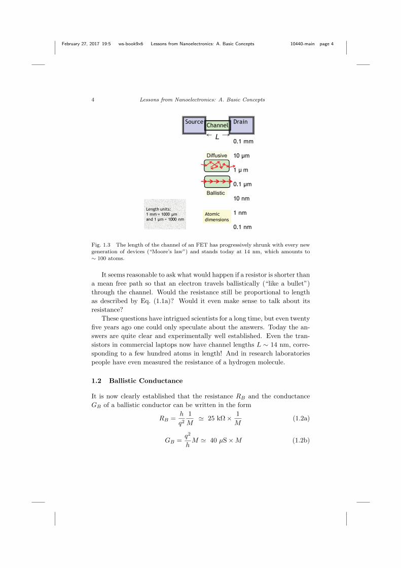
February 27, 2017 19:5 ws-book9x6 Lessons from Nanoelectronics: A. Basic Concepts 10440-main page 4
4 Lessons from Nanoelectronics: A. Basic Concepts
Length units:1 mm = 1000 µmand 1 µm = 1000 nm
ChannelSource Drain
0.1 mm
10 µm
1 µ m
0.1 µm
10 nm
1 nm
0.1 nm
Atomicdimensions
Fig. 1.3 The length of the channel of an FET has progressively shrunk with every newgeneration of devices (“Moore’s law”) and stands today at 14 nm, which amounts to
∼ 100 atoms.
It seems reasonable to ask what would happen if a resistor is shorter than
a mean free path so that an electron travels ballistically (“like a bullet”)
through the channel. Would the resistance still be proportional to length
as described by Eq. (1.1a)? Would it even make sense to talk about its
resistance?
These questions have intrigued scientists for a long time, but even twenty
five years ago one could only speculate about the answers. Today the an-
swers are quite clear and experimentally well established. Even the tran-
sistors in commercial laptops now have channel lengths L ∼ 14 nm, corre-
sponding to a few hundred atoms in length! And in research laboratories
people have even measured the resistance of a hydrogen molecule.
1.2 Ballistic Conductance
It is now clearly established that the resistance RB and the conductance
GB of a ballistic conductor can be written in the form
RB =h
q2
1
M' 25 kΩ× 1
M(1.2a)
GB =q2
hM ' 40 µS×M (1.2b)
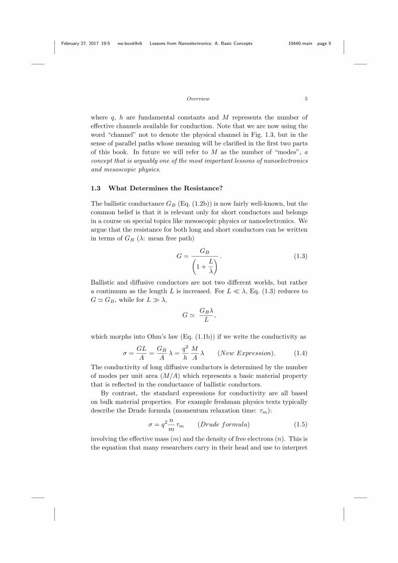
February 27, 2017 19:5 ws-book9x6 Lessons from Nanoelectronics: A. Basic Concepts 10440-main page 5
Overview 5
where q, h are fundamental constants and M represents the number of
effective channels available for conduction. Note that we are now using the
word “channel” not to denote the physical channel in Fig. 1.3, but in the
sense of parallel paths whose meaning will be clarified in the first two parts
of this book. In future we will refer to M as the number of “modes”, a
concept that is arguably one of the most important lessons of nanoelectronics
and mesoscopic physics.
1.3 What Determines the Resistance?
The ballistic conductance GB (Eq. (1.2b)) is now fairly well-known, but the
common belief is that it is relevant only for short conductors and belongs
in a course on special topics like mesoscopic physics or nanoelectronics. We
argue that the resistance for both long and short conductors can be written
in terms of GB (λ: mean free path)
G =GB(
1 +L
λ
) . (1.3)
Ballistic and diffusive conductors are not two different worlds, but rather
a continuum as the length L is increased. For L λ, Eq. (1.3) reduces to
G ' GB , while for L λ,
G ' GBλ
L,
which morphs into Ohm’s law (Eq. (1.1b)) if we write the conductivity as
σ =GL
A=GBA
λ =q2
h
M
Aλ (New Expression). (1.4)
The conductivity of long diffusive conductors is determined by the number
of modes per unit area (M/A) which represents a basic material property
that is reflected in the conductance of ballistic conductors.
By contrast, the standard expressions for conductivity are all based
on bulk material properties. For example freshman physics texts typically
describe the Drude formula (momentum relaxation time: τm):
σ = q2 n
mτm (Drude formula) (1.5)
involving the effective mass (m) and the density of free electrons (n). This is
the equation that many researchers carry in their head and use to interpret
February 27, 2017 19:5 ws-book9x6 Lessons from Nanoelectronics: A. Basic Concepts 10440-main page 6
6 Lessons from Nanoelectronics: A. Basic Concepts
experimental data. However, it is tricky to apply if the electron dynamics
is not described by a simple positive effective mass m. A more general
but less well-known expression for the conductivity involves the density of
states (D) and the diffusion coefficient (D)
σ = q2 D
ALD (Degenerate Einstein relation). (1.6)
In Part 1 of this book we will use fairly elementary arguments to establish
the new formula for conductivity given by Eq. (1.4) and show its equivalence
to Eq. (1.6). In Part 2 we will introduce an energy band model and relate
Eqs. (1.4) and (1.6) to the Drude formula (Eq. (1.5)) under the appropriate
conditions when an effective mass can be defined.
We could combine Eqs. (1.3) and (1.4) to say that the standard Ohm’s
law (Eqs. (1.1)) should be replaced by the result
G =σA
L+ λ→ R =
ρ
A(L+ λ), (1.7)
suggesting that the ballistic resistance (corresponding to L λ) is equal
to ρλ/A which is the resistance of a channel with resistivity ρ and length
equal to the mean free path λ.
But this can be confusing since neither resistivity nor mean free path
are meaningful for a ballistic channel. It is just that the resistivity of a
diffusive channel is inversely proportional to the mean free path, and the
product ρλ is a material property that determines the ballistic resistance
RB . A better way to write the resistance is from the inverse of Eq. (1.3):
R = RB
(1 +
L
λ
). (1.8)
This brings us to a key conceptual question that caused much debate and
discussion in the 1980s and still seems less than clear! Let me explain.
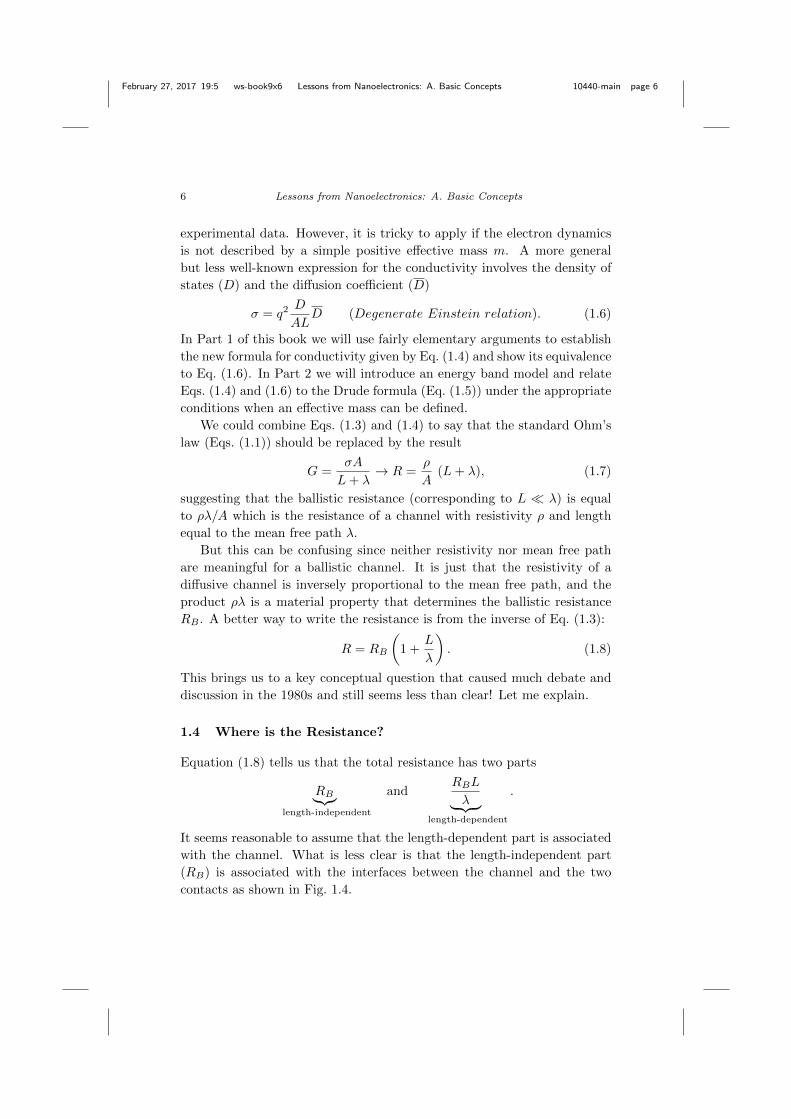
1.4 Where is the Resistance?
Equation (1.8) tells us that the total resistance has two parts
RB︸︷︷︸length-independent
andRBL
λ︸ ︷︷ ︸length-dependent
.
It seems reasonable to assume that the length-dependent part is associated
with the channel. What is less clear is that the length-independent part
(RB) is associated with the interfaces between the channel and the two
contacts as shown in Fig. 1.4.
February 27, 2017 19:5 ws-book9x6 Lessons from Nanoelectronics: A. Basic Concepts 10440-main page 7
Overview 7
How can we split up the overall resistance into different components
and pinpoint them spatially? If we were talking about a large everyday
resistor, the approach is straightforward: we simply look at the voltage
drop across the structure. Since the same current flows everywhere, the
voltage drop at any point should be proportional to the resistance at that
point ∆V = I∆R. A resistance localized at the interface should also give
a voltage drop localized at the interface as shown in Fig. 1.4.
Fig. 1.4 The length-dependent part of the resistance in Eq. (1.8) is associated with thechannel while the length-independent part is associated with the interfaces between the
channel and the two contacts. Shown below is the spatial profile of the “potential” which
supports the spatial distribution of resistances shown.
What makes this discussion not so straightforward in the context of
nanoscale conductors is that it is not obvious how to draw a spatial poten-
tial profile on a nanometer scale. The key question is well-known in the
context of electronic devices, namely the distinction between the electro-
static potential and the electrochemical potential.
February 27, 2017 19:5 ws-book9x6 Lessons from Nanoelectronics: A. Basic Concepts 10440-main page 8
8 Lessons from Nanoelectronics: A. Basic Concepts
The former is related to the electric field F
F = −dφdz,
since the force on an electron is qF , it seems natural to think that the
current should be determined by dφ/dz. However, it is well-recognized that
this is only of limited validity at best. More generally current is driven by
the gradient in the electrochemical potential :
I
A≡ J = −σ
q
dµ
dz. (1.9)
Just as heat flows from higher to lower temperatures, electrons flow from
higher to lower electrochemical potentials giving an electron current that
is proportional to −dµ/dz. It is only under special conditions that µ and φ
track each other and one can be used in place of the other. Although the
importance of electrochemical potentials and quasi-Fermi levels is well es-
tablished in the context of device physics, many experts feel uncomfortable
about using these concepts on a nanoscale and prefer to use the electro-
static potential instead. However, I feel that this obscures the underlying
physics and considerable conceptual clarity can be achieved by defining
electrochemical potentials and quasi-Fermi levels carefully on a nanoscale.
The basic concepts are now well established with careful experimen-
tal measurements of the potential drop across nanoscale defects (see for
example, Willke et al. 2015). Theoretically it was shown using a full quan-
tum transport formalism (which we discuss in part B) that a suitably de-
fined electrochemical potential shows abrupt drops at the interfaces, while
the corresponding electrostatic potential is smoothed out over a screening
length making the resulting drop less obvious (Fig. 1.5). These ideas are
described in simple semiclassical terms (following Datta 1995) in Part 3 of
this volume.
1.5 But Where is the Heat?
One often associates the electrochemical potential with the energy of the
electrons, but at the nanoscale this viewpoint is completely incompatible
with what we are discussing. The problem is easy to see if we consider an
ideal ballistic channel with a defect or a barrier in the middle, which is the
problem Rolf Landauer posed in 1957.
Common sense says that the resistance is caused largely by the barrier
and we will show in Chapter 10 that a suitably defined electrochemical

February 27, 2017 19:5 ws-book9x6 Lessons from Nanoelectronics: A. Basic Concepts 10440-main page 9
Overview 9
ElectrochemicalPotential
ElectrostaticPotential
qV
µ1 µ2
Fig. 1.5 Spatial profile of electrostatic and electrochemical potentials in a nanoscaleconductor using a quantum transport formalism. Reproduced from McLennan et al.
1991.
Fig. 1.6 Potential profile across a ballistic channel with a hole in the middle.
potential indeed shows a spatial profile that shows a sharp drop across the
barrier in addition to abrupt drops at the interfaces as shown in Fig. 1.6.
If we associate this electrochemical potential with the energy of the
electrons then an abrupt potential drop across the barrier would be ac-
companied by an abrupt drop in the energy, implying that heat is being
dissipated locally at the scatterer. This requires the energy to be trans-
ferred from the electrons to the lattice so as to set the atoms jiggling which
manifests itself as heat. But a scatterer does not necessarily have the de-
February 27, 2017 19:5 ws-book9x6 Lessons from Nanoelectronics: A. Basic Concepts 10440-main page 10
10 Lessons from Nanoelectronics: A. Basic Concepts
grees of freedom needed to dissipate energy: it could for example be just a
hole in the middle of the channel with no atoms to “jiggle.”
In short, the resistance R arises from the loss of momentum caused in
this case by the “hole” in the middle of the channel. But the dissipation
I2R could occur very far from the hole and the potential in Fig. 1.6 cannot
represent the energy. So what does it represent?
The answer is that the electrochemical potential represents the degree
of filling of the available states, so that it indicates the number of electrons
and not their energy. It is then easy to understand the abrupt drop across
a barrier which represents a bottleneck on the electronic highway. As we
all know there are traffic jams right before a bottleneck, but as soon as we
cross it, the road is all empty: that is exactly what the potential profile in
Fig. 1.6 indicates!
In short, everyone would agree that a “hole” in an otherwise ballistic
channel is the cause and location of the resulting resistance and an elec-
trochemical potential defined to indicate the number of electrons correlates
well with this intuition. But this does not indicate the location of the
dissipation I2R.
The hole in the channel gives rise to “hot” electrons with a non-
equilibrium energy distribution which relaxes back to normal through a
complex process of energy exchange with the surroundings over an energy
relaxation length LE ∼ tens of nanometers or longer. The process of dissi-
pation may be of interest in its own right, but it does not help locate the
hole that caused the loss of momentum which gave rise to resistance in the
first place.
1.6 Elastic Resistors
Once we recognize the spatially distributed nature of dissipative processes
it seems natural to model nanoscale resistors shorter than LE as an ideal
elastic resistor which we define as one in which all the energy exchange
and dissipation occurs in the contacts and none within the channel itself
(Fig. 1.7).
For a ballistic resistor RB , as my colleague Ashraf often points out, it
is almost obvious that the corresponding Joule heat I2R must occur in the
contacts. After all a bullet dissipates most of its energy to the object it
hits rather than to the medium it flies through.
There is experimental evidence that real nanoscale conductors do ac-
tually come close to this idealized model which has become widely used

February 27, 2017 19:5 ws-book9x6 Lessons from Nanoelectronics: A. Basic Concepts 10440-main page 11
Overview 11
ChannelSource Drain
V +- I
Heat
HeatNo exchange
of energy
Fig. 1.7 The ideal elastic resistor with the Joule heat V I = I2R generated entirely inthe contacts as sketched. Many nanoscale conductors are believed to be close to this
ideal.
ever since the advent of mesoscopic physics in the late 1980s and is often
referred to as the Landauer approach. However, it is generally believed
that this viewpoint applies only to near-ballistic transport and to avoid
this association we are calling it an elastic resistor rather than a Landauer
resistor.
What we wish to stress is that even a diffusive conductor full of “pot-
holes” that destroy momentum could in principle dissipate all the Joule
heat in the contacts. And even if it does not, its resistance can be calcu-
lated accurately from an idealized model that assumes it does. Indeed we
will use this elastic resistor model to obtain the conductivity expression in
Eq. (1.4) and show that it agrees well with the standard results.
But surely we cannot ignore all the dissipation inside a long resistor
and calculate its resistance accurately treating it as an elastic resistor? We
believe we can do so in many cases of interest, especially at low bias. The
underlying issues can be understood qualitatively using the simple circuit
model shown in Fig. 1.8. For an elastic resistor each energy channel E1,
E2 and E3 is independent with no flow of electrons between them as shown
on the left. Inelastic processes induce “vertical” flow between the energy
channels represented by the vertical resistors as shown on the right. When
can we ignore the vertical resistors?
If the series of resistors representing individual channels are identical,
then the nodes connected by the vertical resistors will be at the same po-
tential, so that there will be no current flow through them. Under these
conditions, an elastic resistor model that ignores the vertical resistors is
quite accurate.

February 27, 2017 19:5 ws-book9x6 Lessons from Nanoelectronics: A. Basic Concepts 10440-main page 12
12 Lessons from Nanoelectronics: A. Basic Concepts
μ1 μ2 μ2μ1Fig. 1.8 A simple circuit model: (a) For elastic resistors, individual energy channels
E1, E2 and E3 are decoupled with no flow between them. (b) Inelastic processes causevertical flow between energy channels through the additional resistors shown.
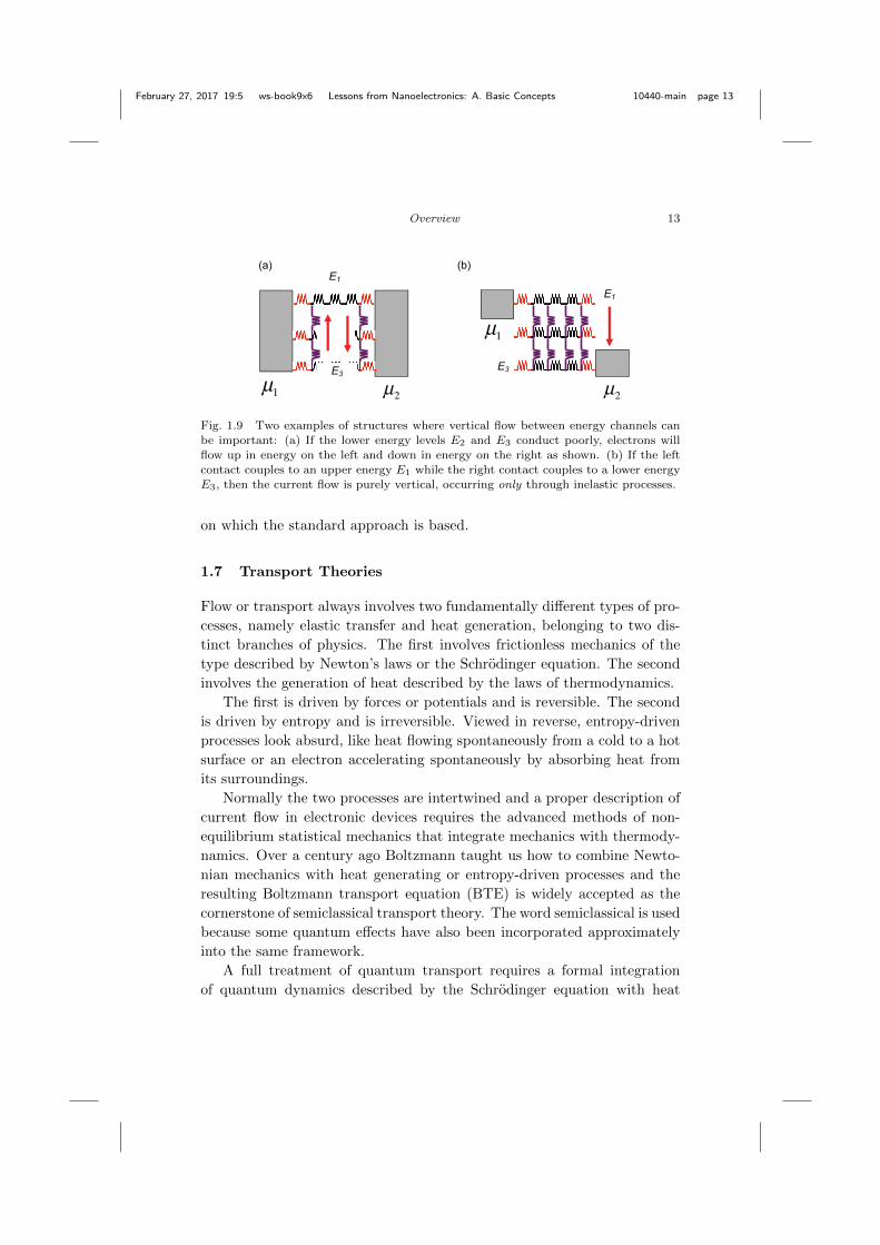
But vertical flow cannot always be ignored. For example, Fig. 1.9a
shows a conductor where the lower energy levels E2 and E3 conduct poorly
compared to E1. We would then expect the electrons to flow upwards in
energy on the left and downwards in energy on the right as shown, thus
cooling the lattice on the left and heating the lattice on the right, leading
to the well-known Peltier effect discussed in Chapter 13.
The role of vertical flow can be even more striking if the left contact
connects only to the channel E1 while the right contact connects only to
E3 as shown in Fig. 1.9b. No current can flow in such a structure without
vertical flow, and the entire current is purely a vertical current. This is
roughly what happens in p-n junctions which is discussed a little further in
Section 12.1.
The bottom line is that elastic resistors generally provide a good de-
scription of short conductors and the Landauer approach has become quite
common in mesoscopic physics and nanoelectronics. What is not well recog-
nized is that this approach can provide useful results even for long conduc-
tors. In many cases, but not always, we can ignore inelastic processes and
calculate the resistance quite accurately as long as the momentum relax-
ation has been correctly accounted for, as discussed further in Section 3.3.
But why would we want to ignore inelastic processes? Why is the theory
of elastic resistors any more straightforward than the standard approach?
To understand this we first need to talk briefly about the transport theories
February 27, 2017 19:5 ws-book9x6 Lessons from Nanoelectronics: A. Basic Concepts 10440-main page 13
Overview 13
μ2
μ1
μ2μ1Fig. 1.9 Two examples of structures where vertical flow between energy channels can
be important: (a) If the lower energy levels E2 and E3 conduct poorly, electrons willflow up in energy on the left and down in energy on the right as shown. (b) If the left
contact couples to an upper energy E1 while the right contact couples to a lower energy
E3, then the current flow is purely vertical, occurring only through inelastic processes.
on which the standard approach is based.
1.7 Transport Theories
Flow or transport always involves two fundamentally different types of pro-
cesses, namely elastic transfer and heat generation, belonging to two dis-
tinct branches of physics. The first involves frictionless mechanics of the
type described by Newton’s laws or the Schrodinger equation. The second
involves the generation of heat described by the laws of thermodynamics.
The first is driven by forces or potentials and is reversible. The second
is driven by entropy and is irreversible. Viewed in reverse, entropy-driven
processes look absurd, like heat flowing spontaneously from a cold to a hot
surface or an electron accelerating spontaneously by absorbing heat from
its surroundings.
Normally the two processes are intertwined and a proper description of
current flow in electronic devices requires the advanced methods of non-
equilibrium statistical mechanics that integrate mechanics with thermody-
namics. Over a century ago Boltzmann taught us how to combine Newto-
nian mechanics with heat generating or entropy-driven processes and the
resulting Boltzmann transport equation (BTE) is widely accepted as the
cornerstone of semiclassical transport theory. The word semiclassical is used
because some quantum effects have also been incorporated approximately
into the same framework.
A full treatment of quantum transport requires a formal integration
of quantum dynamics described by the Schrodinger equation with heat

February 27, 2017 19:5 ws-book9x6 Lessons from Nanoelectronics: A. Basic Concepts 10440-main page 14
14 Lessons from Nanoelectronics: A. Basic Concepts
ClassicalDynamics BTE+ =
generating processes.
QuantumDynamics NEGF+ =
This is exactly what is achieved in the non-equilibrium Green’s function
(NEGF) method originating in the 1960s from the seminal works of Martin
and Schwinger (1959), Kadanoff and Baym (1962), Keldysh (1965) and
others.
1.7.1 Why elastic resistors are conceptually simpler
The BTE takes many semesters to master and the full NEGF formalism,
even longer. Much of this complexity comes from the subtleties of combin-
ing mechanics with distributed heat-generating processes.
Channel
The operation of the elastic resistor can be understood in far more
elementary terms because of the clean spatial separation between the force-
driven and the entropy-driven processes. The former is confined to the
channel and the latter to the contacts. As we will see in the next few
chapters, the latter is easily taken care of, indeed so easily that it is easy
to miss the profound nature of what is being accomplished.
Even quantum transport can be discussed in relatively elementary terms
using this viewpoint. For example, Fig. 1.10 shows a plot of the spatial
profile of the electrochemical potential across our structure from Fig. 1.6
with a hole in the middle, calculated both from the semiclassical BTE
(Chapter 9) and from the NEGF method (part B).
For the NEGF method we show three options. First a coherent model
(left) that ignores all interaction within the channel showing oscillations
indicative of standing waves. Once we include phase relaxation, the con-
structive and destructive interferences are lost and we obtain the result in

February 27, 2017 19:5 ws-book9x6 Lessons from Nanoelectronics: A. Basic Concepts 10440-main page 15
Overview 15
- V +“barrier”
qVa)
b)
c)
f
f
Fig. 1.10 Spatial profile of the electrochemical potential across a channel with a barrier.Solid red line indicates semiclassical result from BTE (part A). Also shown are the
results from NEGF (part B) assuming (a) coherent transport, (b) transport with phase
relaxation, (c) transport with phase and momentum relaxation. Note that no energyrelaxation is included in any of these calculations.
February 27, 2017 19:5 ws-book9x6 Lessons from Nanoelectronics: A. Basic Concepts 10440-main page 16
16 Lessons from Nanoelectronics: A. Basic Concepts
the middle which approaches the semiclassical result. If the interactions
include momentum relaxation as well we obtain a profile indicative of an
additional distributed resistance.
None of these models includes energy relaxation and they all qualify
as elastic resistors making the theory much simpler than a full quantum
transport model that includes dissipative processes. Nevertheless, they all
exhibit a spatial variation in the electrochemical potential consistent with
our intuitive understanding of resistance.
A good part of my own research in the past was focused in this area
developing the NEGF method, but we will get to it only in part B after we
have “set the stage” in this volume using a semiclassical picture.
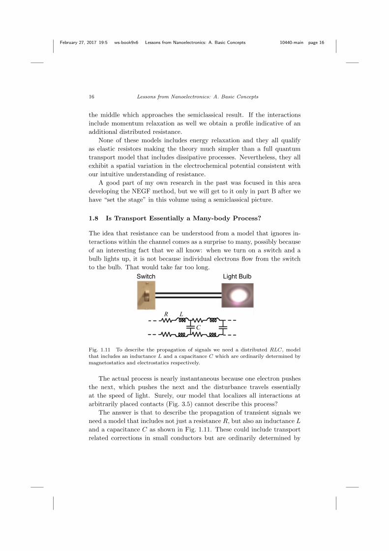
1.8 Is Transport Essentially a Many-body Process?
The idea that resistance can be understood from a model that ignores in-
teractions within the channel comes as a surprise to many, possibly because
of an interesting fact that we all know: when we turn on a switch and a
bulb lights up, it is not because individual electrons flow from the switch
to the bulb. That would take far too long.
R L
C
Switch Light Bulb
Fig. 1.11 To describe the propagation of signals we need a distributed RLC, model
that includes an inductance L and a capacitance C which are ordinarily determined bymagnetostatics and electrostatics respectively.
The actual process is nearly instantaneous because one electron pushes
the next, which pushes the next and the disturbance travels essentially
at the speed of light. Surely, our model that localizes all interactions at
arbitrarily placed contacts (Fig. 3.5) cannot describe this process?
The answer is that to describe the propagation of transient signals we
need a model that includes not just a resistance R, but also an inductance L
and a capacitance C as shown in Fig. 1.11. These could include transport
related corrections in small conductors but are ordinarily determined by
February 27, 2017 19:5 ws-book9x6 Lessons from Nanoelectronics: A. Basic Concepts 10440-main page 17
Overview 17
magnetostatics and electrostatics respectively (Salahuddin et al. 2005).
In this distributedRLC transmission line, the signal velocity determined
by L and C can be well in excess of individual electron velocities reflecting a
collective process. However, L and C play no role at low frequencies, since
the inductor is then like a “short circuit” and the capacitor is like an “open
circuit.” The low frequency conduction properties are represented solely by
the resistance R and can usually be understood fairly well in terms of the
transport of individual electrons along M parallel modes (see Eqs. (1.2))
or “channels”, a concept that has emerged from decades of research. To
quote Phil Anderson from a volume commemorating 50 years of Anderson
localization (see Anderson (2010)):
“ . . . What might be of modern interest is the “channel” concept which
is so important in localization theory. The transport properties at low fre-
quencies can be reduced to a sum over one-dimensional “channels” . . . ”
1.9 A Different Physical Picture
Let me conclude this overview with an obvious question: why should we
bother with idealized models and approximate physical pictures? Can’t we
simply use the BTE and the NEGF equations which provide rigorous frame-
works for describing semiclassical and quantum transport respectively? The
answer is yes, and all the results we discuss are benchmarked against the
BTE and the NEGF.
However, as Feynman (1963) noted in his classic lectures, even when
we have an exact mathematical formulation, we need an intuitive physical
picture:
“.. people .. say .. there is nothing which is not contained in the equa-
tions .. if I understand them mathematically inside out, I will understand
the physics inside out. Only it doesn’t work that way. .. A physical under-
standing is a completely unmathematical, imprecise and inexact thing, but
absolutely necessary for a physicist.”
Indeed, most researchers carry a physical picture in their head and it is
usually based on the Drude formula (Eq. (1.5)). In this book we will show
that an alternative picture based on elastic resistors leads to a formula
(Eq. (1.4)) that is more generally valid.
February 27, 2017 19:5 ws-book9x6 Lessons from Nanoelectronics: A. Basic Concepts 10440-main page 18
18 Lessons from Nanoelectronics: A. Basic Concepts
Unlike the Drude formula which treats the electric field as the driving
term, this new approach more correctly treats the electrochemical poten-
tial as the driving term. This is well-known at the macroscopic level, but
somehow seems to have been lost in nanoscale transport, where people cite
the difficulty of defining electrochemical potentials. However, that does not
justify using electric field as a driving term, an approach that does not work
for inhomogeneous conductors on any scale.
Since all conductors are fundamentally inhomogeneous on an atomic
scale it seems questionable to use electric field as a driving term. We argue
that at least for low bias transport, it is possible to define electrochemi-
cal potentials or quasi-Fermi levels on an atomic scale and this can lend
useful insight into the physics of current flow and the origin of resistance.
We believe this is particularly timely because future electronic devices will
require a clear understanding of the different potentials.
For example, recent work on spintronics has clearly established experi-
mental situations where upspin and downspin electrons have different elec-
trochemical potentials (sometimes called quasi-Fermi levels) and could even
flow in opposite directions because their dµ/dz have opposite signs. This
cannot be understood if we believe that currents are driven by electric fields,
−dφ/dz, since up and down spins both see the same electric field and have
the same charge. We can expect to see more and more such examples that
use novel contacts to manipulate the quasi-Fermi levels of different group
of electrons (see Chapter 12 for further discussion).
In short we believe that the lessons of nanoelectronics lead naturally
to a new viewpoint, one that changes even some basic concepts we all
learn in freshman physics. This viewpoint represents a departure from the
established mindset and I hope it will provide a complementary perspective
to facilitate the insights needed to take us to the next level of discovery and
innovation.
February 27, 2017 19:5 ws-book9x6 Lessons from Nanoelectronics: A. Basic Concepts 10440-main page 19
PART 1
What Determines the Resistance
19

February 27, 2017 19:5 ws-book9x6 Lessons from Nanoelectronics: A. Basic Concepts 10440-main page 20
February 27, 2017 19:5 ws-book9x6 Lessons from Nanoelectronics: A. Basic Concepts 10440-main page 21
Chapter 2
Why Electrons Flow
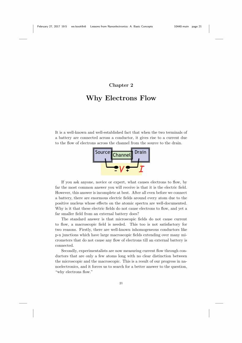
It is a well-known and well-established fact that when the two terminals of
a battery are connected across a conductor, it gives rise to a current due
to the flow of electrons across the channel from the source to the drain.
ChannelSource Drain
V +- IIf you ask anyone, novice or expert, what causes electrons to flow, by
far the most common answer you will receive is that it is the electric field.
However, this answer is incomplete at best. After all even before we connect
a battery, there are enormous electric fields around every atom due to the
positive nucleus whose effects on the atomic spectra are well-documented.
Why is it that these electric fields do not cause electrons to flow, and yet a
far smaller field from an external battery does?
The standard answer is that microscopic fields do not cause current
to flow, a macroscopic field is needed. This too is not satisfactory for
two reasons. Firstly, there are well-known inhomogeneous conductors like
p-n junctions which have large macroscopic fields extending over many mi-
crometers that do not cause any flow of electrons till an external battery is
connected.
Secondly, experimentalists are now measuring current flow through con-
ductors that are only a few atoms long with no clear distinction between
the microscopic and the macroscopic. This is a result of our progress in na-
noelectronics, and it forces us to search for a better answer to the question,
“why electrons flow.”
21
February 27, 2017 19:5 ws-book9x6 Lessons from Nanoelectronics: A. Basic Concepts 10440-main page 22
22 Lessons from Nanoelectronics: A. Basic Concepts
2.1 Two Key Concepts
Related video lecture available at course website, Unit 1: L1.2.
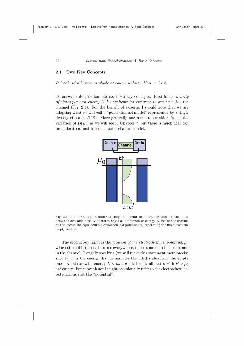
To answer this question, we need two key concepts. First is the density
of states per unit energy D(E) available for electrons to occupy inside the
channel (Fig. 2.1). For the benefit of experts, I should note that we are
adopting what we will call a “point channel model” represented by a single
density of states D(E). More generally one needs to consider the spatial
variation of D(E), as we will see in Chapter 7, but there is much that can
be understood just from our point channel model.
ChannelSource Drain
μ0 E
D(E)
Fig. 2.1 The first step in understanding the operation of any electronic device is to
draw the available density of states D(E) as a function of energy E, inside the channeland to locate the equilibrium electrochemical potential µ0 separating the filled from the
empty states.
The second key input is the location of the electrochemical potential, µ0
which at equilibrium is the same everywhere, in the source, in the drain, and
in the channel. Roughly speaking (we will make this statement more precise
shortly) it is the energy that demarcates the filled states from the empty
ones. All states with energy E < µ0 are filled while all states with E > µ0
are empty. For convenience I might occasionally refer to the electrochemical
potential as just the “potential”.
February 27, 2017 19:5 ws-book9x6 Lessons from Nanoelectronics: A. Basic Concepts 10440-main page 23
Why Electrons Flow 23
μ1
μ2
E
q V
D(E)
ChannelSource Drain
V +- I
Fig. 2.2 When a voltage is applied across the contacts, it lowers all energy levels at thepositive contact (drain in the picture). As a result the electrochemical potentials in the
two contacts separate: µ1 − µ2 = qV .
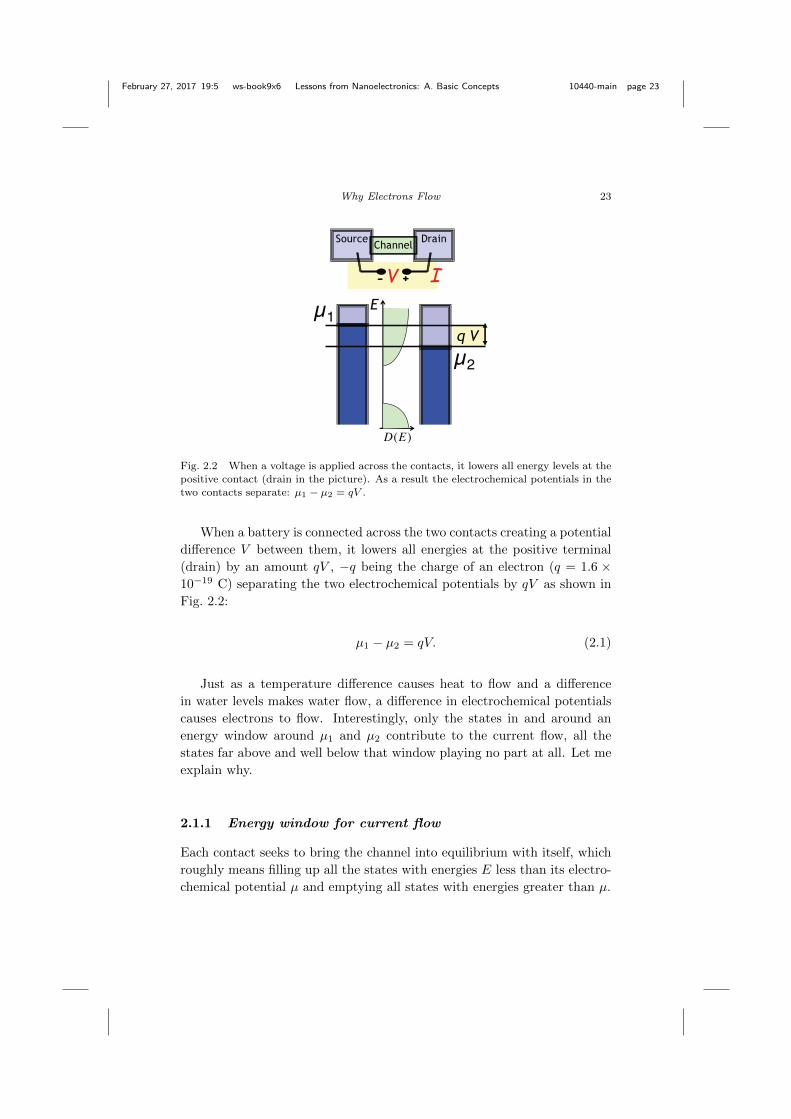
When a battery is connected across the two contacts creating a potential
difference V between them, it lowers all energies at the positive terminal
(drain) by an amount qV , −q being the charge of an electron (q = 1.6 ×10⁻¹⁹ C) separating the two electrochemical potentials by qV as shown in
Fig. 2.2:
µ1 − µ2 = qV. (2.1)
Just as a temperature difference causes heat to flow and a difference
in water levels makes water flow, a difference in electrochemical potentials
causes electrons to flow. Interestingly, only the states in and around an
energy window around µ1 and µ2 contribute to the current flow, all the
states far above and well below that window playing no part at all. Let me
explain why.
2.1.1 Energy window for current flow
Each contact seeks to bring the channel into equilibrium with itself, which
roughly means filling up all the states with energies E less than its electro-
chemical potential µ and emptying all states with energies greater than µ.

February 27, 2017 19:5 ws-book9x6 Lessons from Nanoelectronics: A. Basic Concepts 10440-main page 24
24 Lessons from Nanoelectronics: A. Basic Concepts
Consider the states with energy E that are less than µ1 but greater
than µ2. Contact 1 wants to fill them up since E < µ1, but contact 2 wants
to empty them since E > µ2. And so contact 1 keeps filling them up and
contact 2 keeps emptying them causing electrons to flow continually from
contact 1 to contact 2.
Consider now the states with E greater than both µ1 and µ2. Both
contacts want these states to remain empty and they simply remain empty
with no flow of electrons. Similarly the states with E less than both µ1 and
µ2 do not cause any flow either. Both contacts like to keep them filled and
they just remain filled. There is no flow of electrons outside the window
between µ1 and µ2, or more correctly outside ± a few kT of this window,
as we will discuss shortly.
This last point may seem obvious, but often causes much debate because
of the common belief we alluded to earlier, namely that electron flow is
caused by the electric field in the channel. If that were true, all the electrons
should flow and not just the ones in any specific window determined by the
contacts.
2.2 Fermi Function
Let us now make the above statements more precise. We stated that roughly
speaking, at equilibrium, all states with energies E below the electrochem-
ical potential µ are filled while all states with E > µ are empty. This
is precisely true only at absolute zero temperature. More generally, the
transition from completely full to completely empty occurs over an energy
range ∼ ± 2 kT around E = µ where k is the Boltzmann constant (∼ 80
µeV/K) and T is the absolute temperature. Mathematically, this transition
is described by the Fermi function:
f(E) =1
exp
(E − µkT
)+ 1
. (2.2)
This function is plotted in Fig. 2.3 (left panel), though in an unconventional
form with the energy axis vertical rather than horizontal. This will allow
us to place it alongside the density of states, when trying to understand
current flow (see Fig. 2.4).
For readers unfamiliar with the Fermi function, let me note that an
extended discussion is needed to do justice to this deep but standard result,
and we will discuss it a little further in Chapter 15 when we talk about the
key principles of equilibrium statistical mechanics. At this stage it may

February 27, 2017 19:5 ws-book9x6 Lessons from Nanoelectronics: A. Basic Concepts 10440-main page 25
Why Electrons Flow 25
E μ
kT
f (E) kTf
E
Fermi function,Eq.(2.2)
Normalized thermalbroadening function,
Eq.(2.3)
Fig. 2.3 Fermi function and the normalized (dimensionless) thermal broadeningfunction.
help to note that what this function (Fig. 2.3) basically tells us is that
states with low energies are always occupied (f = 1), while states with
high energies are always empty (f = 0), something that seems reasonable
since we have heard often enough that (1) everything goes to its lowest
energy, and (2) electrons obey an exclusion principle that stops them from
all getting into the same state. The additional fact that the Fermi function
tells us is that the transition from f = 1 to f = 0 occurs over an energy
range of ∼ ±2 kT around µ0.
2.2.1 Thermal broadening function
Also shown in Fig. 2.3 is the derivative of the Fermi function, multiplied by
kT to make it dimensionless. Using Eq. (2.2) it is straightforward to show
that
FT (E,µ) = kT
(− ∂f∂E
)=
ex
(ex + 1)2(2.3)
where x ≡ E − µkT
.
Note: (1) From Eq. (2.3) it follows that
FT (E,µ) = FT (E − µ) = FT (µ− E). (2.4)
February 27, 2017 19:5 ws-book9x6 Lessons from Nanoelectronics: A. Basic Concepts 10440-main page 26
26 Lessons from Nanoelectronics: A. Basic Concepts
(2) From Eqs. (2.3) and (2.2) it follows that
FT = f(1− f). (2.5)
(3) If we integrate FT over all energy the total area equals kT :∫ +∞
−∞dE FT (E,µ) = kT
∫ +∞
−∞dE
(− ∂f∂E
)
= kT [−f ]+∞−∞ = kT (1− 0) = kT (2.6)
so that we can approximately visualize FT as a rectangular “pulse” centered
around E = µ with a peak value of 1/4 and a width of ∼ 4 kT .
2.3 Non-equilibrium: Two Fermi Functions
When a system is in equilibrium the electrons are distributed among the
available states according to the Fermi function. But when a system is
driven out-of-equilibrium there is no simple rule for determining the dis-
tribution of electrons. It depends on the specific problem at hand making
non-equilibrium statistical mechanics far richer and less understood than
its equilibrium counterpart.
For our specific non-equilibrium problem, we argue that the two contacts
are such large systems that they cannot be driven out-of-equilibrium. And
so each remains locally in equilibrium with its own electrochemical potential
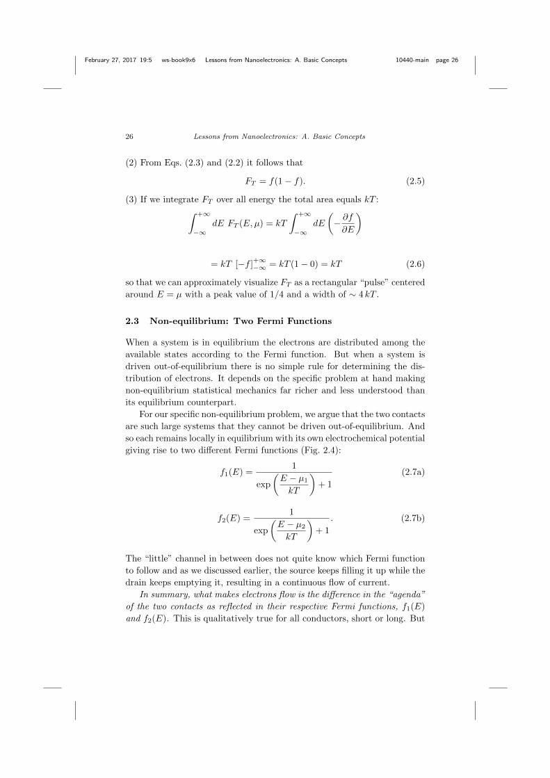
giving rise to two different Fermi functions (Fig. 2.4):
f1(E) =1
exp
(E − µ1
kT
)+ 1
(2.7a)
f2(E) =1
exp
(E − µ2
kT
)+ 1
. (2.7b)
The “little” channel in between does not quite know which Fermi function
to follow and as we discussed earlier, the source keeps filling it up while the
drain keeps emptying it, resulting in a continuous flow of current.
In summary, what makes electrons flow is the difference in the “agenda”
of the two contacts as reflected in their respective Fermi functions, f1(E)
and f2(E). This is qualitatively true for all conductors, short or long. But
February 27, 2017 19:5 ws-book9x6 Lessons from Nanoelectronics: A. Basic Concepts 10440-main page 27
Why Electrons Flow 27
for short conductors, the current at any given energy E is quantitatively
proportional to
I(E) ∼ f1(E)− f2(E) (2.8)
representing the difference in the occupation probabilities in the two con-
tacts. This quantity goes to zero when E lies way above µ1 and µ2, since f1
and f2 are both zero. It also goes to zero when E lies way below µ1 and µ2,
since f1 and f2 are both one. Current flow occurs only in the intermediate
energy window, as we had argued earlier.
f2(E)f1(E)
μ2
E/kT
μ1
D(E)
Fig. 2.4 Electrons in the contacts occupy the available states with a probability de-
scribed by a Fermi function f(E) with the appropriate electrochemical potential µ.
2.4 Linear Response
Current-voltage relations are typically not linear, but there is a common
approximation that we will frequently use throughout this book to extract
the “linear response” which refers to the low bias conductance, dI/dV ,
as V → 0. The basic idea can be appreciated by plotting the difference
between two Fermi functions, normalized to the applied voltage
F (E) =f1(E)− f2(E)
qV/kT(2.9)
where
µ1 = µ0 + (qV/2)
µ2 = µ0 − (qV/2).
Figure 2.5 shows that the difference function F gets narrower as the voltage
is reduced relative to kT . The interesting point is that as qV is reduced

February 27, 2017 19:5 ws-book9x6 Lessons from Nanoelectronics: A. Basic Concepts 10440-main page 28
28 Lessons from Nanoelectronics: A. Basic Concepts
below kT , the function F approaches the thermal broadening function FTwe defined (see Eq. (2.3)) in Section 2.2.1:
F (E)→ FT (E), as qV/kT → 0
so that from Eq. (2.9)
f1(E)− f2(E) ≈ qV
kTFT (E,µ0) =
(−∂f0
∂E
)qV (2.10)
if the applied voltage µ1 − µ2 = qV is much less than kT .
F(E)
y<1
y=3y=7
y qV / kT
E μ0kT
Fig. 2.5 F (E) from Eq. (2.9) versus (E − µ0)/kT for different values of y = qV/kT .
The validity of Eq. (2.10) for qV kT can be checked numerically
if you have access to MATLAB or equivalent. For those who like to see a
mathematical derivation, Eq. (2.10) can be obtained using the Taylor series
expansion described in Appendix A to write
f(E)− f0(E) ≈(−∂f0
∂E
)(µ− µ0) (2.11)
Eq. (2.11) and Eq. (2.10) which follows from it, will be used frequently in
these lectures.

February 27, 2017 19:5 ws-book9x6 Lessons from Nanoelectronics: A. Basic Concepts 10440-main page 29
Why Electrons Flow 29
2.5 Difference in “Agenda” Drives the Flow
Before moving on, let me quickly reiterate the key point we are trying to
make, namely that the current is determined by
−∂f0(E)
∂Eand NOT by f0(E).
The two functions look similar over a limited range of energies
−∂f0(E)
∂E≈ f0(E)
kTif E − µ0 kT.
So if we are dealing with a so-called non-degenerate conductor (see Sec-
tion 3.4) where we can restrict our attention to a range of energies satisfying
this criterion, we may not notice the difference.
In general these functions look very different (see Fig. 2.3) and the
experts agree that current depends not on the Fermi function, but on its
derivative. However, we are not aware of an elementary treatment that
leads to this result and consequently our everyday thinking tends to be
dominated by a different picture.
2.5.1 Drude formula
Related video lecture available at course website, Unit 1: L1.9.
For example, freshman physics texts start by treating the force due to an
electric field F as the driving term and adding a frictional term to Newton’s
law (τm is the so-called “momentum relaxation time”)
d(mν)
dt= (−qF ) − mν
τm.
Newton′s Law Friction
At steady-state (d/dt = 0) this gives a non-zero drift velocity,
νd = − q τmm︸ ︷︷ ︸
mobility, µ
× F (2.12)
from which one calculates the electron current using the relation
I
A= qnνd = − qnµ︸︷︷︸
conductivity, σ
× F. (2.13)

February 27, 2017 19:5 ws-book9x6 Lessons from Nanoelectronics: A. Basic Concepts 10440-main page 30
30 Lessons from Nanoelectronics: A. Basic Concepts
The negative sign appears in Eq. (2.13) because we use “I” to denote the
electron current (see Section 3.2.2) which flows opposite to the electric field.
Equations (2.12) and (2.13) lead to the Drude formula, stated earlier in
Eq. (1.5), which plays a key role in defining our mental picture of current
flow. Since the above approach treats electric fields as the driving term, it
also suggests that the current depends on the total number of electrons since
all electrons feel the field. This is commonly explained away by saying that
there are mysterious quantum mechanical forces that prevent electrons in
full bands from moving and what matters is the number of “free electrons”.
But this begs the question of which electrons are free and which are not, a
question that becomes more confusing for atomic scale conductors.
It is well-known that the conductivity varies widely, changing by a factor
of ∼ 1020 going from copper to glass, to mention two materials that are near
two ends of the spectrum. But this is not because one has more electrons
than the other. The total number of electrons is of the same order of
magnitude for all materials from copper to glass. Whether a material is a
good or a bad conductor is determined by the availability of states in an
energy window ∼ kT around the electrochemical potential µ0, which can
vary widely from one material to another. This is well-known to experts
and comes mathematically from the dependence of the conductivity
on − ∂f0
∂Erather than f0(E)
a result that typically requires advanced treatments based on the Boltz-
mann equation (Chapter 9) or the fluctuation-dissipation theorem (Chap-
ter 5).
2.5.2 Present approach
We obtain this result in an elementary way as we have just seen. Current is
driven by the difference in the “agenda” of the two contacts which for low
bias is proportional to the derivative of the equilibrium Fermi function:
f1(E)− f2(E) ≈(−∂f0
∂E
)qV.
There is no need to invoke mysterious forces that stops some electrons from
moving, though one could perhaps call it a mysterious force, since the Fermi
function (Eq. (2.2)) reflects the exclusion principle.
Later when we (briefly) discuss phonon transport in Chapter 14, we will
see how this approach is readily extended to describe the flow of phonons.
The phonon current is governed by the Bose (not Fermi) function which is
appropriate for particles that do not have an exclusion principle.

February 27, 2017 19:5 ws-book9x6 Lessons from Nanoelectronics: A. Basic Concepts 10440-main page 31
Chapter 3
The Elastic Resistor
Related video lectures available at course website, Unit 1: L1.3 and L1.4.
We saw in the last chapter that the flow of electrons is driven by the dif-
ference in the “agenda” of the two contacts as reflected in their respective
Fermi functions, f1(E) and f2(E). The negative contact with its larger f(E)
would like to see more electrons in the channel than the positive contact.
And so the positive contact keeps withdrawing electrons from the channel
while the negative contact keeps pushing them in. This is true of all con-
ductors, big and small. But in general, it is difficult to express the current
as a simple function of f1(E) and f2(E), because electrons jump around
from one energy to another and the current flow at different energies is all
mixed up.
μ2μ1
Fig. 3.1 An elastic resistor: electrons travel along fixed energy channels.
But for the ideal elastic resistor shown in Fig. 3.1, the current in an
energy range from E to E+ dE is decoupled from that in any other energy
range, allowing us to write it in the form
dI ∼ dE G(E) (f1(E)− f2(E))
and integrating it to obtain the total current I. Making use of Eq. (2.10),
31
February 27, 2017 19:5 ws-book9x6 Lessons from Nanoelectronics: A. Basic Concepts 10440-main page 32
32 Lessons from Nanoelectronics: A. Basic Concepts
this leads to an expression for the low bias conductance
I
V=
∫ +∞
−∞dE
(−∂f0
∂E
)G(E) (3.1)
where −(∂f0/∂E) can be visualized as a rectangular pulse of area equal to
one, with a width of ∼ 4 kT around µ (see Fig. 2.3, right panel).
Equation (3.1) tells us that for an elastic resistor, we can define a con-
ductance function G(E) whose average over an energy range ∼ ± 2kT
around the electrochemical potential µ0 gives the experimentally measured
conductance. At low temperatures, we can simply use the value of G(E)
at E = µ0.
This energy-resolved view of conductance represents an enormous sim-
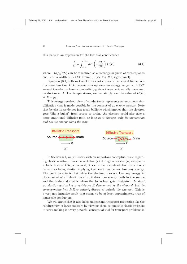
plification that is made possible by the concept of an elastic resistor. Note
that by elastic we do not just mean ballistic which implies that the electron
goes “like a bullet” from source to drain. An electron could also take a
more traditional diffusive path as long as it changes only its momentum
and not its energy along the way:
Source Drain
Ballistic Transport
(a)
Source Drain
Diffusive Transport
(b)
In Section 3.1, we will start with an important conceptual issue regard-
ing elastic resistors: Since current flow (I) through a resistor (R) dissipates
a Joule heat of I2R per second, it seems like a contradiction to talk of a
resistor as being elastic, implying that electrons do not lose any energy.
The point to note is that while the electron does not lose any energy in
the channel of an elastic resistor, it does lose energy both in the source
and the drain and that is where the Joule heat gets dissipated. In short
an elastic resistor has a resistance R determined by the channel, but the
corresponding heat I2R is entirely dissipated outside the channel. This is
a very non-intuitive result that seems to be at least approximately true of
nanoscale conductors.
We will argue that it also helps understand transport properties like the
conductivity of large resistors by viewing them as multiple elastic resistors
in series making it a very powerful conceptual tool for transport problems in

February 27, 2017 19:5 ws-book9x6 Lessons from Nanoelectronics: A. Basic Concepts 10440-main page 33
The Elastic Resistor 33
general. In Section 3.2 we will proceed to obtain our conductance formula
G(E) =q2D(E)
2t(E)(3.2)
expressing the conductance function G(E) for an elastic resistor in terms of
the density of states D(E) and the time t(E) that an electron spends in the
channel. Equation (3.2) seems quite intuitive: it says that the conductance
is proportional to the product of two factors, namely the availability of
states (D) and the ease with which electrons can transport through them
(1/t). This is the key result that we will use in subsequent chapters.
Finally in Section 3.3 we will explain how the energy averaging of the
conductance function G(E) described by Eq. (3.1) leads to two different
limiting physical pictures, generally referred to as the degenerate and the
non-degenerate limits. Although the semiconductor literature often focuses
on the non-degenerate limit, we will try to keep the discussion general so
that it applies to both limits and in-between as well.
3.1 How an Elastic Resistor Dissipates Heat
Let us start by addressing a basic question regarding an elastic resistor.
How does it dissipate the joule heat I2R associated with the resistance R?
Consider a one level elastic resistor having one sharp level with energy
ε. Every time an electron crosses over through the channel, it appears as
a “hot electron” on the drain side with an energy ε in excess of the local
electrochemical potential µ2 as shown below:
μ1μ2
Source Drain
(a) Temporary state immediatelyafter electron transfer
(a)
qV
(b) Final state after energyrelaxation processes have
returned contacts to equilibrium
(b)
Energy dissipating processes in the contact quickly make the electron
get rid of the excess energy (ε− µ2). Similarly at the source end an empty
spot (a “hole”) is left behind with an energy that is much less than the
local electrochemical potential µ1, which gets quickly filled up by electrons
dissipating the excess energy (µ1 − ε).

February 27, 2017 19:5 ws-book9x6 Lessons from Nanoelectronics: A. Basic Concepts 10440-main page 34
34 Lessons from Nanoelectronics: A. Basic Concepts
In effect, every time an electron crosses over from the source to the
drain,
an energy (µ1 − ε) is dissipated at the sourcean energy (ε− µ2) is dissipated at the drain.
The total energy dissipated is
µ1 − µ2 = qV
which is supplied by the external battery that maintains the potential dif-
ference µ1 − µ2. The overall flow of electrons and heat is summarized in
Fig. 3.2.
Flow of Electronsand Heat
ChannelSource
µ1 µ2
Heat Heat
Drain
μ1μ2
Fig. 3.2 Flow of electrons and heat in a one-level elastic resistor having one level with
E = ε.
If N electrons cross over in a time t
Current, I =qN
t
Dissipated power =qV N
t= V I.
Note that V I is the same as I2R and V 2G.
The heat dissipated by an “elastic resistor” thus occurs in the contacts.
As we will see next, the detailed mechanism underlying the complicated
process of heat transfer in the contacts can be completely bypassed simply
by legislating that the contacts are always maintained in equilibrium with
a fixed electrochemical potential.
3.2 Current in an Elastic Resistor
Consider an elastic resistor (Fig. 3.1) with an arbitrary density of states
D(E). Since all energy channels conduct independently in parallel, we
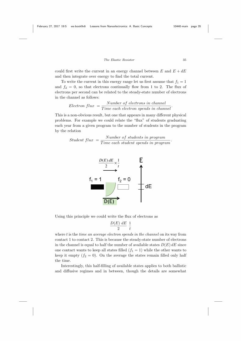
February 27, 2017 19:5 ws-book9x6 Lessons from Nanoelectronics: A. Basic Concepts 10440-main page 35
The Elastic Resistor 35
could first write the current in an energy channel between E and E + dE
and then integrate over energy to find the total current.
To write the current in this energy range let us first assume that f1 = 1
and f2 = 0, so that electrons continually flow from 1 to 2. The flux of
electrons per second can be related to the steady-state number of electrons
in the channel as follows:
Electron flux =Number of electrons in channel
T ime each electron spends in channel.
This is a non-obvious result, but one that appears in many different physical
problems. For example we could relate the “flux” of students graduating
each year from a given program to the number of students in the program
by the relation
Student flux =Number of students in program
Time each student spends in program.
E
D(E)
D(E) dE
2× 1t
Using this principle we could write the flux of electrons as
D(E) dE
2
1
t
where t is the time an average electron spends in the channel on its way from
contact 1 to contact 2. This is because the steady-state number of electrons
in the channel is equal to half the number of available states D(E) dE since
one contact wants to keep all states filled (f1 = 1) while the other wants to
keep it empty (f2 = 0). On the average the states remain filled only half
the time.
Interestingly, this half-filling of available states applies to both ballistic
and diffusive regimes and in between, though the details are somewhat

February 27, 2017 19:5 ws-book9x6 Lessons from Nanoelectronics: A. Basic Concepts 10440-main page 36
36 Lessons from Nanoelectronics: A. Basic Concepts
E
D(E)
D(E) dE
2× 1t
different in different regimes as we will see later in Chapter 8 when we
discuss the diffusion equation.
If we reverse the roles of the two contacts with f1 = 0 and f2 = 1,
we will have the same flux but in the opposite direction. In general with
arbitrary values of f1 and f2 we can superpose the two results to write the
net current as the difference
dI = qD(E) dE
2t(f1(E)− f2(E))
where we have multiplied by the electronic charge q to convert from flux of
electrons to flux of (negative) charge. Integrating we obtain an expression
for the current through the elastic resistor:
I =1
q
∫ +∞
−∞dE G(E) (f1(E)− f2(E)) (3.3)
where G(E) =q2D(E)
2t(E)→ same as Eq. (3.2).
3.2.1 Exclusion principle?
It is not obvious that in general we can superpose the two results from
f1 = 1, f2 = 0 and from f1 = 0, f2 = 1 and obtain the resulting current as
we have done. Doesn’t the presence of one stream affect the other?
We view electrons as non-interacting particles with the understanding
that their Coulomb interaction is included through an average potential U
which is calculated self-consistently (Chapter 7). But even then it might
seem that the mere presence of one stream could impede the other stream
through the Pauli exclusion principle which can be significant for degenerate
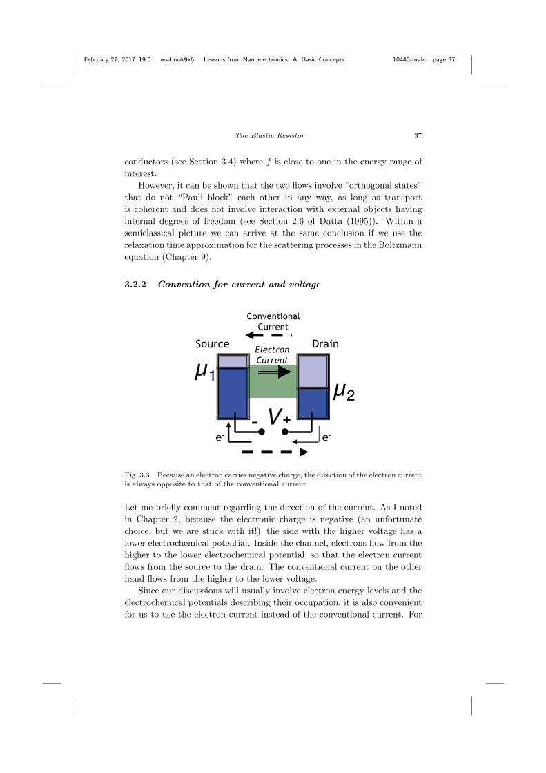
February 27, 2017 19:5 ws-book9x6 Lessons from Nanoelectronics: A. Basic Concepts 10440-main page 37
The Elastic Resistor 37
conductors (see Section 3.4) where f is close to one in the energy range of
interest.
However, it can be shown that the two flows involve “orthogonal states”
that do not “Pauli block” each other in any way, as long as transport
is coherent and does not involve interaction with external objects having
internal degrees of freedom (see Section 2.6 of Datta (1995)). Within a
semiclassical picture we can arrive at the same conclusion if we use the
relaxation time approximation for the scattering processes in the Boltzmann
equation (Chapter 9).
3.2.2 Convention for current and voltage
μ1μ2
Source Drain
ConventionalCurrent
e-e-
V
ElectronCurrent
- +
Fig. 3.3 Because an electron carries negative charge, the direction of the electron currentis always opposite to that of the conventional current.
Let me briefly comment regarding the direction of the current. As I noted
in Chapter 2, because the electronic charge is negative (an unfortunate
choice, but we are stuck with it!) the side with the higher voltage has a
lower electrochemical potential. Inside the channel, electrons flow from the
higher to the lower electrochemical potential, so that the electron current
flows from the source to the drain. The conventional current on the other
hand flows from the higher to the lower voltage.
Since our discussions will usually involve electron energy levels and the
electrochemical potentials describing their occupation, it is also convenient
for us to use the electron current instead of the conventional current. For

February 27, 2017 19:5 ws-book9x6 Lessons from Nanoelectronics: A. Basic Concepts 10440-main page 38
38 Lessons from Nanoelectronics: A. Basic Concepts
example, in Fig. 3.3 it seems natural to say that the current flows from
the source to the drain and not the other way around. And that is what I
will try to do consistently throughout this book. In short, we will use the
current, I, to mean electron current.
3.3 Conductance of a Long Resistor
If the applied bias is much less than kT , we can use Eq. (2.10) to write
from Eq. (3.3)
I = V
∫ +∞
−∞dE
(−∂f0
∂E
)G(E)
which yields the expression for conductance stated earlier in Eq. (3.1). Since
we are obtaining the linear conductance by keeping only the first term in
a Taylor series (Eq. (2.10)), it can be justified only for voltages V < kT/q,
which at room temperature equals 25 mV. But everyday resistors are linear
for voltages that are much larger. How do we explain that?
The answer is that the elastic resistor model should only be applied to
a short length < Lin, where Lin is the length an electron travels on the
average before getting inelastically scattered. Such short conductors could
indeed show non-linear effects for voltages > kT/q, though the non-linearity
may be quite small if the conductance function G(E) is constant over the
relevant energy range (see Section 2.5 of Datta (1995)).
But how do we understand everyday resistors that are linear over sev-
eral volts? To apply the elastic resistor model to a large conductor with
distributed inelastic processes (Fig. 3.4a) we should break it up conceptu-
ally into a sequence of elastic resistors (Fig. 3.4b), each much shorter than
the physical length L, having a voltage that is only a fraction of the total
voltage V . As long as the voltage dropped over a length Lin is less than
kT/q we expect the current to be linear with voltage. The terminal voltage
can be much larger.
Before we move on, let me reiterate a little subtlety in viewing a long
resistor (Fig. 3.4a) as elastic resistors in series (Fig. 3.4b). We will see in
the next chapter that the resistance of an individual section has the form
R = RB
(1 +
L
λ
)→ same as Eq. (1.8) (3.4)
and we will see in Part 3, that the length independent part RB represents
an interface resistance associated with the channel-contact interfaces.

February 27, 2017 19:5 ws-book9x6 Lessons from Nanoelectronics: A. Basic Concepts 10440-main page 39
The Elastic Resistor 39
Inelastic scatterers
μ2μ1
Source Drain
(a)
μ2μ1
L L L
(b)
Fig. 3.4 (a) Real conductors have inelastic scatterers distributed throughout the chan-
nel. (b) A hypothetical series of elastic resistors as an approximation to a real resistorwith distributed inelastic scattering as shown in (a).
Now, the structure in Fig. 3.4b has too many conceptual interfaces that
are not present in the real structure of Fig. 3.4a. Each of these interfaces
introduces an interface resistance as shown in Fig. 3.5 and these have to be
subtracted out. But this is straightforward to do, once we understand the
nature and origin of the interface resistance. For example, the resistance of
the real structure in Fig. 3.4a of length 3L is approximately given by
R = RB
(1 +
3L
λ
)and NOT by R = 3RB
(1 +
L
λ
). (3.5)
In general our approach is to consider just a single section, exclude the
interface resistances to obtain the length dependent part of the resistance
(RBL/λ) from which we deduce bulk properties like the conductivity.
Fig. 3.5 A long resistor can be viewed as a series of ideal elastic resistors. However,
we have to exclude the resistance due to all the conceptual interfaces that we introducewhich are not present in the physical structure.

February 27, 2017 19:5 ws-book9x6 Lessons from Nanoelectronics: A. Basic Concepts 10440-main page 40
40 Lessons from Nanoelectronics: A. Basic Concepts
3.4 Degenerate and Non-degenerate Conductors
Getting back to our conductance expression
I
V=
∫ +∞
−∞dE
(−∂f0
∂E
)G(E) → same as Eq. (3.1)
we note that depending on the nature of the conductance function G(E)
and the thermal broadening function we can identify two distinct limits
(Fig. 3.6).
The first is case A where the conductance function G(E) is nearly con-
stant over the width of the broadening function. We could then pull G(E)
out of the integral in Eq. (3.1) to write
I
V≈ G(E = µ0)
∫ +∞
−∞dE
(−∂f0
∂E
)= G(E = µ0). (3.6)
This relation suggests an operational definition for the conductance function
G(E): it is the conductance measured at low temperatures for a channel
with its electrochemical potential µ0 located at E. The actual conductance
is obtained by averaging G(E) over a range of energies using −∂f0/∂E as
a weighting function. Case A is a good example of the so-called degenerate
conductors.
G(E)
A
B
µ0
4kTf0E
Fig. 3.6 Degenerate (A) and non-degenerate (B) limits.
The other extreme is the non-degenerate conductor shown in case B
where the electrochemical potential is located at an energy many kT ’s below

February 27, 2017 19:5 ws-book9x6 Lessons from Nanoelectronics: A. Basic Concepts 10440-main page 41
The Elastic Resistor 41
the energy range where the conductance function is non-zero. As a result
over the energy range of interest where G(E) is non-zero, we have
x ≡ E − µ0
kT 1
and it is common to approximate the Fermi function with the Boltzmann
function
1
1 + ex≈ e−x
so thatI
V=
∫ +∞
−∞
dE
kTG(E) e−(E−µ0)/kT .
This non-degenerate limit is commonly used in the semiconductor literature
though the actual situation is often intermediate between degenerate and
non-degenerate limits.
We will generally use the expression
G =q2D
2t
with the understanding that the quantities D and t are evaluated at E = µ0
at low temperatures. Depending on the nature of G(E) and the location
of µ0, we may need to average G(E) over a range of energies using as a
“weighting function” as prescribed by Eq. (3.1).

February 27, 2017 19:5 ws-book9x6 Lessons from Nanoelectronics: A. Basic Concepts 10440-main page 42

February 27, 2017 19:5 ws-book9x6 Lessons from Nanoelectronics: A. Basic Concepts 10440-main page 43
Chapter 4
Ballistic and Diffusive Transport
Related video lectures available at course website, Unit 1: L1.5, L1.6, L1.7
and L1.8.
We saw in the last chapter that the resistance of an elastic resistor can be
written as
G =q2D
2t→ same as Eq. (3.2).
In this chapter, I will first argue that the transit time t across a resistor of
length L for diffusive transport with a mean free path can be related to the
time tB for ballistic transport by the relation (Section 4.1)
t = tB
(1 +
L
λ
). (4.1)
Combining with Eq. (3.2) we obtain
G =GBλ
L+ λ(4.2)
where GB =q2D
2tB. (4.3)
We could rewrite Eq. (4.2) as
G =σA
L+ λ(4.4a)
where σA = GBλ. (4.4b)
So far we have only talked about three dimensional resistors with a large
cross-sectional area A. Many experiments involve two-dimensional resistors
43

February 27, 2017 19:5 ws-book9x6 Lessons from Nanoelectronics: A. Basic Concepts 10440-main page 44
44 Lessons from Nanoelectronics: A. Basic Concepts
3-D conductor with2-D cross-section
of area A
L
A
2-D conductor with1-D cross-section
of area W
L
WL
1-D conductor
Current
Fig. 4.1 3D, 2D and 1D conductors.
whose cross-section is effectively one-dimensional with a width W , so that
the appropriate equations have the form
G =σW
L+ λ
where σW = GBλ.
Finally we have one-dimensional conductors for which
G =σ
L+ λ
where σ = GBλ.
We could collect all these results and write them compactly in the form
G =σ
L+ λ1,W,A (4.5a)
where σ = GBλ
1,
1
W,
1
A
. (4.5b)
The three items in parenthesis correspond to 1D, 2D and 3D conductors.
Note that the conductivity has different dimensions in 1D, 2D and 3D,
while both GB and λ have the same dimensions, namely Siemens (S) and
meter (m) respectively.
Note that Eq. (4.5) is different from the standard Ohm’s law
G =σ
L1,W,A
which predicts that the resistance will approach zero (conductance will
become infinitely large) as the length L is reduced to zero. Of course no one
expects it to become zero, but the common belief is that it will approach a

February 27, 2017 19:5 ws-book9x6 Lessons from Nanoelectronics: A. Basic Concepts 10440-main page 45
Ballistic and Diffusive Transport 45
value determined by the interface resistance which can be made arbitrarily
small with improved contacting technology.
What is now well established experimentally is that even with the best
possible contacts, there is a minimum interface resistance determined by
the properties of the channel, independent of the contact. The modified
Ohm’s law in Eq. (4.5) reflects this fact: even a channel of zero length with
perfect contacts has a resistance equal to that of a hypothetical channel of
length λ. But what does it mean to talk about the mean free path of a
channel of zero length? The answer is that neither σ nor λ mean anything
for a short conductor, but the ballistic conductance
GB =σ
λ1, W, A
represents a basic material parameter whose significance has become clear
in the light of modern experiments (see Section 4.2).
The ballistic conductance is proportional to the number of channels,
M(E) available for conduction, which is proportional to, but not the same
as, the density of states, D(E). The concept of density of states has been
with us since the earliest days of solid state physics. By contrast, the
number of channels (or transverse modes) M(E) is a more recent concept
whose significance was appreciated only after the seminal experiments in
the 1980s on ballistic conductors showing conductance quantization.
4.1 Transit Times
Consider how the two quantities in
G =q2D
2t
namely the density of states, D and the transfer time t scale with channel
dimensions for large conductors. The first of these is relatively easy to see
since we expect the number of states to be additive. A channel twice as big
should have twice as many states, so that the density of states D(E) for
large conductors should be proportional to the volume (AL).
Regarding the transfer time, t, broadly speaking there are two transport
regimes:
Ballistic regime: Transfer time t ∼ LDiffusive regime: Transfer time t ∼ L2.
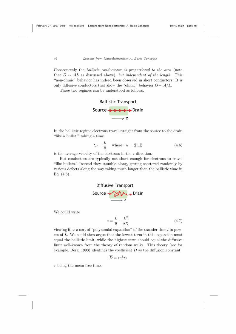
February 27, 2017 19:5 ws-book9x6 Lessons from Nanoelectronics: A. Basic Concepts 10440-main page 46
46 Lessons from Nanoelectronics: A. Basic Concepts
Consequently the ballistic conductance is proportional to the area (note
that D ∼ AL as discussed above), but independent of the length. This
“non-ohmic” behavior has indeed been observed in short conductors. It is
only diffusive conductors that show the “ohmic” behavior G ∼ A/L.
These two regimes can be understood as follows.
Source Drain
Ballistic Transport
In the ballistic regime electrons travel straight from the source to the drain
“like a bullet,” taking a time
tB =L
uwhere u = 〈|vz|〉 (4.6)
is the average velocity of the electrons in the z-direction.
But conductors are typically not short enough for electrons to travel
“like bullets.” Instead they stumble along, getting scattered randomly by
various defects along the way taking much longer than the ballistic time in
Eq. (4.6).
Source Drain
Diffusive Transport
We could write
t =L
u+L2
2D(4.7)
viewing it as a sort of “polynomial expansion” of the transfer time t in pow-
ers of L. We could then argue that the lowest term in this expansion must
equal the ballistic limit, while the highest term should equal the diffusive
limit well-known from the theory of random walks. This theory (see for
example, Berg, 1993) identifies the coefficient D as the diffusion constant
D = 〈v2zτ〉
τ being the mean free time.
February 27, 2017 19:5 ws-book9x6 Lessons from Nanoelectronics: A. Basic Concepts 10440-main page 47
Ballistic and Diffusive Transport 47
Some readers may not find this “polynomial expansion” completely satisfac-
tory. But this approach has the advantage of getting us to the new Ohm’s
law (Eq. (4.5)) very quickly using simple algebra. In Chapters 8 and 9 we
will obtain this result more directly from the Boltzmann equation.
Getting back to Eq. (4.7), we use Eq. (4.6) to rewrite it in the form
t = tB
(1 +
Lu
2D
)which agrees with Eq. (4.1) if the mean free path is given by
λ =2D
u.
In defining the two constants D and u we have used the symbol 〈〉 to
denote an average over the angular distribution of velocities which yields a
different numerical factor depending on the dimensionality of the conductor
(see Appendix B). For d = 1, 2, 3 dimensions
u ≡ 〈|vz|〉 = v(E)
1,
2
π,
1
2
(4.8)
D ≡ 〈v2zτ〉 = v2(E)τ(E)
1,
1
2,
1
3
(4.9)
λ =2D
u= v(E)τ(E)
2,π
2,
4
3
. (4.10)
Note that our definition of the mean free path includes a dimension-
dependent numerical factor over and above the standard value of ντ .
Couldn’t we simply use the standard definition? We could, but then the
new Ohm’s law would not simply involve replacing L with L plus λ. Instead
it would involve L plus a dimension-dependent factor times λ. Instead we
have chosen to absorb this factor into the definition of λ.
Interestingly, even in one dimensional conductors the factor is not one,
but two. This is because the mean free time after which an electron gets
scattered. Assuming the scattering to be isotropic, only half the scattering
events will result in an electron traveling towards the drain to head towards
the source. The mean free time for backscattering is thus, making the mean
free path 2ντ rather than ντ .

February 27, 2017 19:5 ws-book9x6 Lessons from Nanoelectronics: A. Basic Concepts 10440-main page 48
48 Lessons from Nanoelectronics: A. Basic Concepts
4.2 Channels for Conduction
Next we obtain an expression for the ballistic conductance by combining
Eq. (4.3) with Eq. (4.6) to obtain
GB =q2Du
2L
and then make use of Eq. (4.8) to write
GB =q2Dv
2L
1,
2
π,
1
2
(4.11)
Eq. (4.11) tells us that the ballistic conductance depends on D/L, the
density of states per unit length.
Actualconductor withcross-sectional
area A
M independentconductorsIn parallel
•
•Current
L L
A
Fig. 4.2 Channels of conduction: a key concept.
Since D is proportional to the volume, the ballistic conductance is ex-
pected to be proportional to the cross-sectional area A in 3D conductors
(or the width W in 2D conductors). This was experimentally observed in
metals in 1969 and is known as the Sharvin resistance. Numerous exper-
iments since the 1980s have shown that for small conductors, the ballistic
conductance does not go down linearly with the area A. Rather it goes
down in integer multiples of the conductance quantum
GB =q2
h︸︷︷︸∼40µS
× M︸︷︷︸integer
. (4.12)

February 27, 2017 19:5 ws-book9x6 Lessons from Nanoelectronics: A. Basic Concepts 10440-main page 49
Ballistic and Diffusive Transport 49
How can we understand this relation and what does the integer M
represent? This result cannot come out of our elementary treatment of
electrons in classical particle-like terms, since it involves Planck’s constant
h. Some input from quantum mechanics is clearly essential and this will
come in Chapter 6 when we evaluate D(E). For the moment we note that
heuristically Eq. (4.12) suggests that we visualize the real conductor as
M independent channels in parallel whose conductances add up to give
Eq. (4.11) for the ballistic conductance.
This suggests that we use Eqs. (4.12) and (4.11) to define a quantity
M(E) (floor(x) denotes the largest integer less than or equal to x)
M = floor
(hDv
2L
1,
2
π,
1
2
)(4.13)
which provides a measure of the number of conducting channels. In Chap-
ter 6 we will use a simple model that incorporates the wave nature of elec-
trons to show that for a one-dimensional channel the quantity M indeed
equals one showing that it has only one channel, while for two- and three-
dimensional conductors the quantity M represents the number of de Broglie
wavelengths that fit into the cross-section, like the modes of a waveguide.

February 27, 2017 19:5 ws-book9x6 Lessons from Nanoelectronics: A. Basic Concepts 10440-main page 50
February 27, 2017 19:5 ws-book9x6 Lessons from Nanoelectronics: A. Basic Concepts 10440-main page 51
Chapter 5
Conductance from Fluctuation
5.1 Introduction
In this chapter we will digress a little to connect our conductance formula
G =q2D
2t→ same as Eq. (3.2)
to the very powerful fluctuation-dissipation theorem widely used in dis-
cussing linear transport coefficients, like the conductivity. In our discussion
we have stressed the non-equilibrium nature of the problem of current flow
requiring contacts with different electrochemical potentials (see Fig. 2.4).
Just as heat flow is driven by a difference in temperatures, current flow
is driven by a difference in electrochemical potentials. Our basic current
expression (see Eqs. (3.2) and (3.3))
I = q
∫ +∞
−∞dE
D(E)
2t(E)(f1(E)− f2(E)) (5.1)
is applicable to arbitrary voltages but so far we have focused largely on the
low bias approximation (see Eqs. (3.1) and (3.2))
G0 = q2
∫ +∞
−∞dE
(−∂f0
∂E
)D(E)
2t(E)(5.2)
Although we have obtained this result from the general non-equilibrium
expression, it is interesting to note that the low bias conductance is really an
equilibrium property. Indeed there is a fundamental theorem relating the
low bias conductance for small voltages to the fluctuations in the current
that occur at equilibrium when no voltage is applied. Consider a conductor
with no applied voltage (see Fig. 5.1) so that both source and drain have
the same electrochemical potential µ0. There is of course no net current
without an applied voltage, but even at equilibrium, every once in a while,
51

February 27, 2017 19:5 ws-book9x6 Lessons from Nanoelectronics: A. Basic Concepts 10440-main page 52
52 Lessons from Nanoelectronics: A. Basic Concepts
an electron crosses over from source to drain and on the average an equal
number crosses over the other way from the drain to the source, so that
〈I(t0)〉eq = 0
where the angular brackets 〈〉 denote either an “ensemble average” over
many identical conductors or more straightforwardly a time average over
the time t0.
μ0μ0
Source Drain
I(t0)
Fig. 5.1 At equilibrium both contacts have the same electrochemical potential µ0. No
net current flows, but there are equal currents I0 from source to drain and back.
However, if we calculate the current correlation
CI =
∫ +∞
−∞dτ〈I(t0 + τ)I(t0)〉eq (5.3)
we get a non-zero value even at equilibrium, and the fluctuation-dissipation
(F-D) theorem relates this quantity to the low bias conductance:
G0 =CI
2kT=
1
2kT
∫ +∞
−∞dτ〈I(t0 + τ)I(t0)〉eq. (5.4)
This is a very powerful result because it allows one to calculate the conduc-
tance by evaluating the current correlations using the methods of equilib-
rium statistical mechanics, which are in general more well-developed than
the methods of non-equilibrium statistical mechanics. Indeed before the
advent of mesoscopic physics in the late 1980s, the Kubo formula based on
the F-D theorem was the only approach used to model quantum transport.
The Kubo formula in principle applies to large conductors with inelastic
scattering, though in practice it may be difficult to evaluate the effect of
complicated inelastic processes on the current correlation.

February 27, 2017 19:5 ws-book9x6 Lessons from Nanoelectronics: A. Basic Concepts 10440-main page 53
Conductance from Fluctuation 53
Channel
The usual approach is to evaluate transport in long conductors with a
high frequency alternating voltage, for which electrons can slosh back and
forth without ever encountering the contacts. One could then obtain the
zero frequency conductivity by letting the sample size L tend to infinity
before letting the frequency tend to zero (see for example, Chapter 5 of
Doniach and Sondheimer (1974)). However, this approach is limited to
linear response. In this book (part B) we will stress the Non-Equilibrium
Green’s Function (NEGF) method for quantum transport, which allows us
to address the non-equilibrium problem head on for quantum transport,
just as the Boltzmann equation (BTE) does for semiclassical transport.
In this chapter my purpose is primarily to connect our discussion to
this very powerful and widely used approach. We will look at the effect
of contacts on the current correlations in an elastic resistor and show that
applied to an elastic resistor, the F-D theorem (Eq. (5.4)) does lead to our
old result (Eq. (3.2)) from Chapter 3.
Interestingly, our elementary arguments in Chapter 3 lead to a conduc-
tance proportional to
f1 − f2
µ1 − µ2
∼= −∂f0
∂E
while the current correlations in the F-D theorem lead to
f0(1− f0)
kT
with the 1 − f0 factor arising from the exclusion principle. The physical
arguments are very different, but their equivalence is ensured by the identity
− ∂f0
∂E=f0(E)(1− f0(E))
kT(5.5)
which can be verified with a little algebra, starting from the definition of
the Fermi function (Eq. (2.2)).
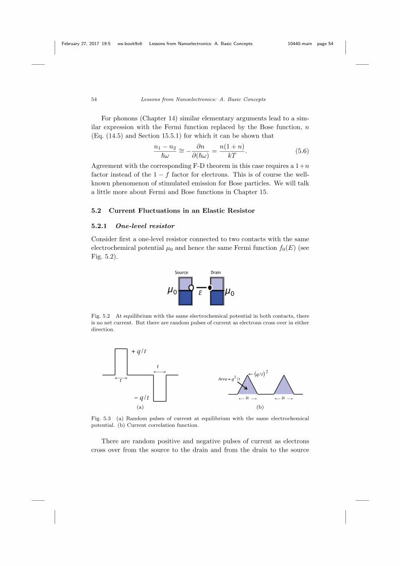
February 27, 2017 19:5 ws-book9x6 Lessons from Nanoelectronics: A. Basic Concepts 10440-main page 54
54 Lessons from Nanoelectronics: A. Basic Concepts
For phonons (Chapter 14) similar elementary arguments lead to a sim-
ilar expression with the Fermi function replaced by the Bose function, n
(Eq. (14.5) and Section 15.5.1) for which it can be shown that
n1 − n2
ω∼= −
∂n
∂(ω)=n(1 + n)
kT. (5.6)
Agreement with the corresponding F-D theorem in this case requires a 1+n
factor instead of the 1 − f factor for electrons. This is of course the well-
known phenomenon of stimulated emission for Bose particles. We will talk
a little more about Fermi and Bose functions in Chapter 15.
5.2 Current Fluctuations in an Elastic Resistor
5.2.1 One-level resistor
Consider first a one-level resistor connected to two contacts with the same
electrochemical potential µ0 and hence the same Fermi function f0(E) (see
Fig. 5.2).
μ0 μ0
Source Drain
Fig. 5.2 At equilibrium with the same electrochemical potential in both contacts, there
is no net current. But there are random pulses of current as electrons cross over in either
direction.
t
+ q / t
t
q / t(a)
q / t( ) 2
2t 2t
Area = q2 / t
(b)
Fig. 5.3 (a) Random pulses of current at equilibrium with the same electrochemicalpotential. (b) Current correlation function.
There are random positive and negative pulses of current as electrons
cross over from the source to the drain and from the drain to the source

February 27, 2017 19:5 ws-book9x6 Lessons from Nanoelectronics: A. Basic Concepts 10440-main page 55
Conductance from Fluctuation 55
respectively. The average positive current is equal to the average negative
current, which we call the equilibrium current I0 and write it in terms of
the transit time t
I0 =q
tf0(ε)(1− f0(ε)) (5.7)
where the factor f0(ε)(1− f0(ε)) is the probability that an electron will be
present at the source ready to transfer to the drain but no electron will be
present at the drain ready to transfer back. The correlation is obtained by
treating the transfer of each electron from the source to the drain as an
independent stochastic process. The integrand in Eq. (5.3) then looks like
a sequence of triangular pulses as shown each having an area of q2/t, so
that
CI = 2q2
tf0(ε)(1− f0(ε)) (5.8)
where the additional factor of 2 comes from the fact that I0 only counts
the positive pulses, while both positive and negative pulses contribute ad-
ditively to CI .
5.2.2 Multi-level resistor
To generalize our one-level results from Eq. (5.7) to an elastic resistor with
an arbitrary density of states, D(E) we note that in an energy range dE
there are D(E) dE states so that
I = q
∫ +∞
−∞dE
D(E)
2t(E)f0(E)(1− f0(E)) (5.9a)
CI = 2q2
∫ +∞
−∞dE
D(E)
2t(E)f0(E)(1− f0(E)) (5.9b)
assuming that the fluctuations in different energy ranges can simply be
added, as we are doing by integrating over energy.
Note that CI = 2qI0 suggesting that the fluctuation is like the shot
noise due to the equilibrium currents I0 flowing in either direction. Making
use of Eq. (5.4) we have for the conductance
G0 =CI
2kT= q2
∫ +∞
−∞dE
f0(E)(1− f0(E))
kT
D(E)
2t(E)(5.10)
which can be reduced to our old expression (see Eqs. (3.1) and (3.2)) making
use of the identity stated earlier in Eq. (5.5).
February 27, 2017 19:5 ws-book9x6 Lessons from Nanoelectronics: A. Basic Concepts 10440-main page 56
56 Lessons from Nanoelectronics: A. Basic Concepts
Before moving on, let me note that there is at present an extensive
body of work on subtle correlation effects in elastic resistors (see for exam-
ple, Splettstoesser et al. 2010), some of which have been experimentally
observed. But the theory of noise even for an elastic resistor is more intri-
cate than the theory for the average current that we will focus on in this
book.

February 27, 2017 19:5 ws-book9x6 Lessons from Nanoelectronics: A. Basic Concepts 10440-main page 57
PART 2
Simple Model for Density of States
57

February 27, 2017 19:5 ws-book9x6 Lessons from Nanoelectronics: A. Basic Concepts 10440-main page 58

February 27, 2017 19:5 ws-book9x6 Lessons from Nanoelectronics: A. Basic Concepts 10440-main page 59
Chapter 6
Energy Band Model
Related video lecture available at course website, Unit 2: L2.10.
6.1 Introduction
A common expression for conductivity is the Drude formula relating the
conductivity to the electron density n, the effective mass m and the mean
free time τ
σ ≡ 1
ρ=q2nτ
m. (6.1)
This expression is very well-known since even freshman physics texts start
by deriving it (see Section 2.5.1). It also leads to the widely used concept
of mobility
µ =qτ
m(6.2)
with σ = qnµ. (6.3)
On the other hand, Eq. (4.5b) expresses the conductivity as a product of
the ballistic conductance GB and the mean free path λ
σ = GBλ
1,
1
W,
1
A
(same as Eq. (4.5b)). (6.4)
This expression can be rewritten, using Eq. (4.3) for GB , Eq. (4.6) for
tB and Eq. (4.10) for λ, as a product of the density of states D and the
diffusion coefficient D (see Eq. (4.9))
σ(E) = q2 DD
L
1,
1
W,
1
A
(6.5)
59

February 27, 2017 19:5 ws-book9x6 Lessons from Nanoelectronics: A. Basic Concepts 10440-main page 60
60 Lessons from Nanoelectronics: A. Basic Concepts
Eq. (6.5) is a standard result referred to as the degenerate Einstein relation
but it is not as well-known as the Drude formula. Most people remember
Eq. (6.1) and not Eq. (6.5). Our objective in this chapter is to relate the
two.
Note that, like the conductance (see Eq. (3.1)), these expressions for
the energy-dependent conductivity also have to be averaged over an energy
range of a few kT ’s around E = µ0, using the thermal broadening function,
σ0 =
∫ +∞
−∞dE
(−∂f0
∂E
)σ(E). (6.6)
It is this averaged conductivity that should be compared to the Drude
conductivity in Eq. (6.1). But for degenerate conductors (see Eq. (3.6))
the averaged conductivity is approximately equal to the conductivity at an
energy E = µ0:
σ0 ≈ σ(E = µ0) (6.7)
and so we can compare σ(E = µ0) from Eq. (6.5) with Eq. (6.1).
The point we wish to stress is that while Eq. (6.1) is often very useful,
it is a result of limited validity that can be obtained from Eq. (6.5) by
making suitable approximations based on a specific model. But when these
approximations are not appropriate, we can still use Eq. (6.5) which is
far more generally applicable .
For example, Eq. (6.5) gives sensible answers even for materials like
graphene whose non-parabolic bands make the meaning of mass somewhat
unclear, causing considerable confusion when using Eq. (6.1). In general we
should really use Eq. (6.5), and not Eq. (6.1), to shape our thinking about
conductivity.
There is a fundamental difference between Eqs. (6.5) and (6.1). The
averaging implied in Eq. (6.6) makes the conductivity a “Fermi surface
property”, that is one that depends only on the energy levels close to E =
µ0. By contrast, Eq. (6.1) depends on the total electron density n integrated
over all energy. But this dependence on the total number is true only in a
limited sense.
Experts know that “n” only represents the density of “free” electrons
and have an instinctive feeling for what it means to be free. They know
that there are p-type semiconductors which conduct better when they have
fewer electrons, but in that case they know that n should be interpreted
to mean the number of “holes”. For beginners, all this appears confusing
and much of this confusion can be avoided by using Eq. (6.5) instead of
Eq. (6.1).

February 27, 2017 19:5 ws-book9x6 Lessons from Nanoelectronics: A. Basic Concepts 10440-main page 61
Energy Band Model 61
Interestingly, Eq. (6.5) was used in a seminal paper to obtain Eq. (3.2)
G(E) =q2D(E)
2t(E)(same as Eq. (3.2)). (6.8)
Equation (1) of Thouless (1977) is essentially the same as this equa-
tion with minor differences in definitions. What we have done is to use
the concept of an elastic resistor to first obtain Eq. (3.2) from elementary
arguments, and then used it to obtain Eq. (6.5).
Equation (6.5) stresses that the essential factor determining the con-
ductivity is the density of states around E = µ0. Materials are known to
have conductivities ranging over many orders of magnitude from glass to
copper. And the basic fact remains that they all have approximately the
same number of electrons. Glass is an insulator but not because it is lacking
in electrons. It is an insulator because it has a very low density of states
or number of modes around E = µ0.
So when does Eq. (6.5) reduce to (6.1)? Answer: if the electrons are
described by a “single band effective mass model” as I will try to show
in this chapter. So far we have kept our discussion general in terms of
the density of states, D(E) and the velocity, v(E) without adopting any
specific models. These concepts are generally applicable even to amorphous
materials and molecular conductors. A vast amount of literature both in
condensed matter physics and in solid state devices, however, is devoted
to crystalline solids with a periodic arrangement of atoms because of the
major role they have played from both basic and applied points of view.
For such materials, energy levels over a limited range of energies are
described by an E(p) relation and we will show in this chapter that irre-
spective of the specific E(p) relation, at any energy E the density of states
D(E), velocity v(E) and momentum p(E) are related to the total num-
ber of states N(E) with energy less than E by the relation (d: number of
dimensions)
D(E)v(E)p(E) = N(E) · d. (6.9)
We can combine this relation with Eq. (6.5) and make use of Eq. (4.9), to
write
σ(E) =q2τ(E)ν(E)
p(E)
N(E)
L,
N(E)
WL,
N(E)
AL
. (6.10)
Equation (6.10) indeed looks like Drude expression (Eq. (6.1)) if we identify
(1) the mass as
m(E) =p(E)
v(E)(6.11)
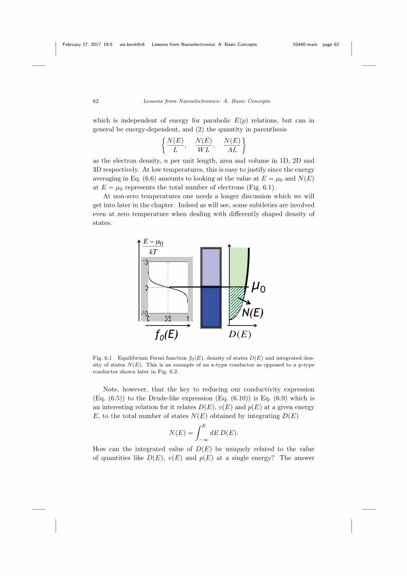
February 27, 2017 19:5 ws-book9x6 Lessons from Nanoelectronics: A. Basic Concepts 10440-main page 62
62 Lessons from Nanoelectronics: A. Basic Concepts
which is independent of energy for parabolic E(p) relations, but can in
general be energy-dependent, and (2) the quantity in parenthesisN(E)
L,
N(E)
WL,
N(E)
AL
as the electron density, n per unit length, area and volume in 1D, 2D and
3D respectively. At low temperatures, this is easy to justify since the energy
averaging in Eq. (6.6) amounts to looking at the value at E = µ0 and N(E)
at E = µ0 represents the total number of electrons (Fig. 6.1).
At non-zero temperatures one needs a longer discussion which we will
get into later in the chapter. Indeed as will see, some subtleties are involved
even at zero temperature when dealing with differently shaped density of
states.
μ0
f0(E) D(E)
E μ0kT
N(E)
Fig. 6.1 Equilibrium Fermi function f0(E), density of states D(E) and integrated den-
sity of states N(E). This is an example of an n-type conductor as opposed to a p-typeconductor shown later in Fig. 6.2.
Note, however, that the key to reducing our conductivity expression
(Eq. (6.5)) to the Drude-like expression (Eq. (6.10)) is Eq. (6.9) which is
an interesting relation for it relates D(E), v(E) and p(E) at a given energy
E, to the total number of states N(E) obtained by integrating D(E)
N(E) =
∫ E
−∞dE D(E).
How can the integrated value of D(E) be uniquely related to the value
of quantities like D(E), v(E) and p(E) at a single energy? The answer

February 27, 2017 19:5 ws-book9x6 Lessons from Nanoelectronics: A. Basic Concepts 10440-main page 63
Energy Band Model 63
is that this relation holds only as long as the energy levels are given by
a single E(p) relation. It may not hold in an energy range with mul-
tiple bands of energies or in an amorphous solid not described by an
E(p) relation. Equation (6.1) is then not equivalent to Eq. (6.5), and
it is Eq. (6.5) that can be trusted .
With that long introduction let us now look at how single bands de-
scribed by an E(p) relation leads to Eq. (6.9) and helps us connect our
conductivity expression (Eq. (6.5)) to the Drude formula (Eq. (6.1)). This
will also lead to a different interpretation of the quantity M(E) introduced
in the last chapter, that will help understand why it is an integer repre-
senting the number of channels.
6.2 E(p) or E(k) Relation
Related video lecture available at course website, Unit 2: L2.2.
The general principle for calculating D(E) is to start from the Schrodinger
equation treating the electron as a wave confined to the solid. Confined
waves (like a guitar string) have resonant “frequencies” and these are ba-
sically the allowed energy levels. By counting the number of energy levels
in a range E to E + dE, we obtain the density of states D(E).
Although the principle is simple, a first principles implementation is
fairly complicated since one needs to start from a Schrodinger equation
including an appropriate potential that the electrons feel inside the solid
not only due to the nuclei but also due to the other electrons.
One of the seminal concepts in solid state physics is the realization that
in crystalline solids electrons behave as if they are in vacuum, but with
an effective mass different from their natural mass, so that the energy-
momentum relation can be written as
E(p) = Ec +p2
2m(6.12)
where Ec is a constant.
The momentum p is equated to ~k, providing the link between the
energy-momentum relation E(p) associated with the particle viewpoint and
the dispersion relation E(k) associated with the wave viewpoint. Here we
will write everything in terms of p, but they are easily translated using the
relation p = ~k.
Equation (6.12) is generally referred to as a parabolic dispersion relation
and is commonly used in a wide variety of materials from metals like copper

February 27, 2017 19:5 ws-book9x6 Lessons from Nanoelectronics: A. Basic Concepts 10440-main page 64
64 Lessons from Nanoelectronics: A. Basic Concepts
E
pEc
ParabolicDispersion
to semiconductors like silicon, because it often approximates the actual E(p)
relation fairly well in the energy range of interest. But it is by no means the
only possibility. Graphene, a material of great current interest, is described
by a linear relation:
E = Ec + v0p (6.13)
where v0 is a constant. Note that p denotes the magnitude of the momen-
tum and we will assume that the E(p) relation is isotropic, which means
that it is the same regardless of which direction the momentum vector
points.
E
pEc
LinearDispersion
For any given isotropic E(p) relation, the velocity points in the same
direction as the momentum, while its magnitude is given by
v ≡ dE
dp. (6.14)

February 27, 2017 19:5 ws-book9x6 Lessons from Nanoelectronics: A. Basic Concepts 10440-main page 65
Energy Band Model 65
This is a general relation applicable to arbitrary energy-momentum rela-
tions for classical particles. On the other hand, in wave mechanics it is jus-
tified as the group velocity for a given dispersion relation E(k). Note that
Eq. (6.14) yields an energy-independent mass m = p/v, only for a parabolic
E(p) relation (Eq. (6.12)) and not for the linear relation in Eq. (6.13).
6.3 Counting States
Related video lecture available at course website, Unit 2: L2.3.
One great advantage of this principle is that it reduces the complicated
problem of electron waves in a solid to that of waves in vacuum, where the
allowed energy levels can be determined the same way we find the resonant
frequencies of a guitar string: simply by requiring that an integer number
of wavelengths fit into the solid. Noting that the de Broglie principle relates
the electron wavelength to the Planck’s constant divided by its momentum,
h/p, we can write
L
h/p= Integer ⇒ p = Integer ×
(h
L
)(6.15)
where L is the length of the box. This means that the allowed states are
uniformly distributed in p with each state occupying a “space” of
4 p =h
L. (6.16)
Let us define a function N(p) that tells us the total number of states
that have a momentum less than a given value p. In one dimension this
function is written down by dividing the total range of 2p (from −p to +p)
by the spacing h/L:
N(p) =2p
h/L= 2L
( ph
)→ 1D.
In two dimensions we divide the area of a circle of radius p by the spacing
h/L× h/W , L and W being the dimensions of the two dimensional box.
N(p) =πp2
(h/L)(h/W )= πWL
( ph
)2
→ 2D.
In three dimensions we divide the volume of a sphere of radius p by the
spacing h/L × h/W1 × h/W2, L, W1 and W2 being the dimensions of the
three dimensional box. Writing A = W1 ×W2 we have
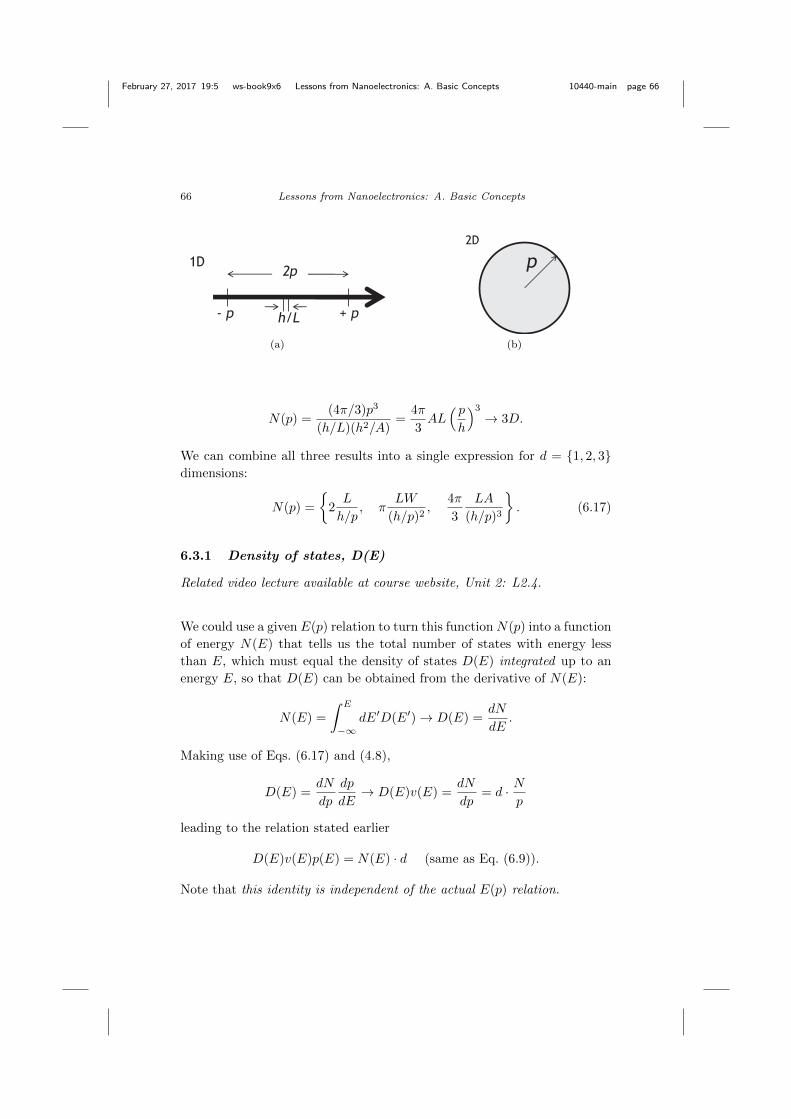
February 27, 2017 19:5 ws-book9x6 Lessons from Nanoelectronics: A. Basic Concepts 10440-main page 66
66 Lessons from Nanoelectronics: A. Basic Concepts
- p + p
2p
h/L
1D
(a)
p2D
(b)
N(p) =(4π/3)p3
(h/L)(h2/A)=
4π
3AL
( ph
)3
→ 3D.
We can combine all three results into a single expression for d = 1, 2, 3dimensions:
N(p) =
2L
h/p, π
LW
(h/p)2,
4π
3
LA
(h/p)3
. (6.17)
6.3.1 Density of states, D(E)
Related video lecture available at course website, Unit 2: L2.4.
We could use a given E(p) relation to turn this function N(p) into a function
of energy N(E) that tells us the total number of states with energy less
than E, which must equal the density of states D(E) integrated up to an
energy E, so that D(E) can be obtained from the derivative of N(E):
N(E) =
∫ E
−∞dE′D(E′)→ D(E) =
dN
dE.
Making use of Eqs. (6.17) and (4.8),
D(E) =dN
dp
dp
dE→ D(E)v(E) =
dN
dp= d · N
p
leading to the relation stated earlier
D(E)v(E)p(E) = N(E) · d (same as Eq. (6.9)).
Note that this identity is independent of the actual E(p) relation.
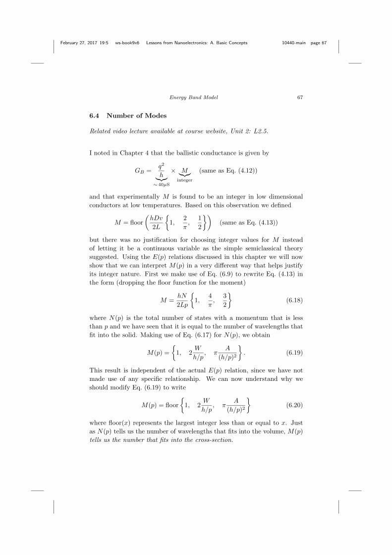
February 27, 2017 19:5 ws-book9x6 Lessons from Nanoelectronics: A. Basic Concepts 10440-main page 67
Energy Band Model 67
6.4 Number of Modes
Related video lecture available at course website, Unit 2: L2.5.
I noted in Chapter 4 that the ballistic conductance is given by
GB =q2
h︸︷︷︸∼ 40µS
× M︸︷︷︸integer
(same as Eq. (4.12))
and that experimentally M is found to be an integer in low dimensional
conductors at low temperatures. Based on this observation we defined
M = floor
(hDv
2L
1,
2
π,
1
2
)(same as Eq. (4.13))
but there was no justification for choosing integer values for M instead
of letting it be a continuous variable as the simple semiclassical theory
suggested. Using the E(p) relations discussed in this chapter we will now
show that we can interpret M(p) in a very different way that helps justify
its integer nature. First we make use of Eq. (6.9) to rewrite Eq. (4.13) in
the form (dropping the floor function for the moment)
M =hN
2Lp
1,
4
π,
3
2
(6.18)
where N(p) is the total number of states with a momentum that is less
than p and we have seen that it is equal to the number of wavelengths that
fit into the solid. Making use of Eq. (6.17) for N(p), we obtain
M(p) =
1, 2
W
h/p, π
A
(h/p)2
. (6.19)
This result is independent of the actual E(p) relation, since we have not
made use of any specific relationship. We can now understand why we
should modify Eq. (6.19) to write
M(p) = floor
1, 2
W
h/p, π
A
(h/p)2
(6.20)
where floor(x) represents the largest integer less than or equal to x. Just
as N(p) tells us the number of wavelengths that fits into the volume, M(p)
tells us the number that fits into the cross-section.
February 27, 2017 19:5 ws-book9x6 Lessons from Nanoelectronics: A. Basic Concepts 10440-main page 68
68 Lessons from Nanoelectronics: A. Basic Concepts
If we evaluate our expressions for N(p) and M(p) for a given sample
we will in general get a fractional number. However, since these quantities
represent the number of states, we would expect them to be integers and if
we obtain say 201.59, we should take the lower integer 201.
This point is commonly ignored in large conductors at high tempera-
tures, where experiments do not show this quantization because of the en-
ergy averaging over µ0 ± 2kT associated with experimental measurements.
For example, if over this energy range, M(E) varies from say 201.59 to
311.67, then it seems acceptable to ignore the fact that it really varies from
201 to 311.
But in small structures where one or more dimensions is small enough
to fit only a few wavelengths the integer nature of M is observable and
shows up in the quantization of the ballistic conductance. We should then
use Eq. (6.20) and not (6.19).
6.4.1 Degeneracy factor
One little “detail” that we need to take into account when comparing to
experiment is the degeneracy factor “g” denoting the number of equivalent
states given by the product of the number of spins and the number of valleys
(which we will discuss in Part B). All these g channels conduct in parallel
so that ballistic conductors have a resistance of
h
q2M≈ 25 kΩ
M
1
g.
So the resistance of a 1D ballistic conductor is approximately equal to 25 kΩ
divided by g. This has indeed been observed experimentally. Most metals
and semiconductors like GaAs have g = 2 due to the two spins, and the 1D
ballistic resistance ∼ 12.5 kΩ. But carbon nanotubes have two valleys as
well making g = 4 and exhibit a ballistic resistance ∼ 6.25 kΩ.
Another “detail” to note is that for two- and three-dimensional conduc-
tors, Eq. (6.17) is not quite right, because it is based on the heuristic idea
of counting modes by counting the number of wavelengths that fit into the
solid (see Eq. (6.15)). Mathematically it can be justified only if we assume
periodic boundary conditions, that is if we assume that the cross-section
is in the form of a ring rather than a flat sheet for a 2D conductor. For
a 3D conductor it is hard to visualize what periodic boundary conditions
might look like though it is easy to impose it mathematically as we have
been doing.

February 27, 2017 19:5 ws-book9x6 Lessons from Nanoelectronics: A. Basic Concepts 10440-main page 69
Energy Band Model 69
Ring-shapedconductor
(a)
FlatConductor
(b)
Most real conductors do not come in the form of rings, yet periodic
boundary conditions are widely used because it is mathematically conve-
nient and people believe that the actual boundary conditions do not really
matter. But this is true only if the cross-section is large. For small area
conductors the actual boundary conditions do matter and we cannot use
Eq. (6.15).
Interestingly a conductor of great current interest has actually been
studied in both forms: a ring-shaped form called a carbon nanotube and a
flat form called graphene. If the circumference or width is tens of nanome-
ters they have much the same properties, but if it is a few nanometers their
properties are observably different including their ballistic resistances.
6.5 Electron Density, n
Related video lecture available at course website, Unit 2: L2.6.
As we mentioned in the introduction, a key quantity appearing in the fa-
miliar Drude formula is the electron density, n. In this Section we would
like to establish that the total number of electrons can be identified with
the function N(E) discussed in Section 6.2. This is easy to see at low
temperatures where the energy averaging in Eq. (6.6) amounts to looking
at the value at a single energy E = µ0. Since N(E) represents the total
number of states available below E, and the total number of electrons at
low temperatures equals the number of states below µ0, it seems clear that
N(E) can be identified with the number of electrons. It then follows that
the electron density can be written as
n(E) = N(E)
1
L,
1
WL,
1
AL
. (6.21)
But does this work at non-zero temperatures? We will argue below that
the answer is yes.

February 27, 2017 19:5 ws-book9x6 Lessons from Nanoelectronics: A. Basic Concepts 10440-main page 70
70 Lessons from Nanoelectronics: A. Basic Concepts
6.5.1 n-type conductors
Will we get the correct electron density if we energy average n(E) from
Eq. (6.21) following the prescription in Eq. (6.6)? It is straightforward to
check that the answer is yes, if we carry out the integral “by parts” to yield∫ +∞
−∞dE
(−∂f0
∂E
)N(E) = [−N(E) f0(E)]
+∞−∞ +
∫ +∞
−∞dE
(dN
dE
)f0(E)
= [0− 0] +
∫ +∞
−∞dE D(E)f0(E)
= Total Number of Electrons
since dED(E)f0(E) tells us the number of electrons in the energy range
from E to E+dE. When integrated it gives us the total number of electrons.
6.5.2 p-type conductors
An interesting subtlety is involved when we consider a p-type conductor for
which the E(p) relation extends downwards, say something like
E(p) = Ev −p2
2m.
Instead of
N(E) =
∫ E
−∞dE′ D(E′)
we now have (see Fig. 6.2)
N(E) =
∫ +∞
E
dE′ D(E′)→ D(E) = −dNdE
.
This is because we defined the function N(E) from N(p) which represents
the total number of states with momenta less than p, which means energies
greater than E for a p-type dispersion relation. Now if we carry out the
integration by parts as before∫ +∞
−∞dE
(−∂f0
∂E
)N(E) = [−N(E) f0(E)]
+∞−∞ +
∫ +∞
−∞dE
(dN
dE
)f0(E)
we run into a problem because the first term does not vanish at the lower
limit where both N(E) and f0(E) are both non-zero. We can get around

February 27, 2017 19:5 ws-book9x6 Lessons from Nanoelectronics: A. Basic Concepts 10440-main page 71
Energy Band Model 71
μ0
f0(E) D(E)
E μ0kT N(E)
Fig. 6.2 Equilibrium Fermi function f0(E), density of states D(E) and integrated den-sity of states N(E): p-type conductor.
this problem by writing the derivative in terms of 1− f0 instead of f0:∫ +∞
−∞dE
(∂(1− f0)
∂E
)N(E)
= [−N(E) (1− f0(E))]+∞−∞ +
∫ +∞
−∞dE
dN
dE[1− f0(E)]
= [0− 0] +
∫ +∞
−∞dE D(E) [1− f0(E)]
= Total Number of “holes”.
What this means is that with p-type conductors we can use the Drude
formula Eq. (6.1)
σ = q2nτ/m
but the n now represents the density of empty states or holes. A larger n
really means fewer electrons.
6.5.3 “Double-ended” density of states
How would we count n for a density of states D(E) that extends in both di-
rections as shown in Fig. 6.3 (left panel). This is representative of graphene,
a material of great interest (recognized by the 2010 Nobel prize in physics),
whose E(p) relation is commonly approximated by
E = ±v0 p.

February 27, 2017 19:5 ws-book9x6 Lessons from Nanoelectronics: A. Basic Concepts 10440-main page 72
72 Lessons from Nanoelectronics: A. Basic Concepts
People usually come up with clever ways to handle such “double-ended”
density of states so that the Drude formula can be used. For example they
divide the total density of states into an n-type and a p-type component
D(E) = Dn(E) +Dp(E)
as shown in Fig. 6.3 and the two components are then handled separately,
using a prescription that is less than obvious: the conductivity due to the
upper half Dn depends on the number of occupied states (electrons), while
that due to the lower half depends on the number of unoccupied states
(holes). But the point we would like to stress is that there is really no
particular reason to insist on using a Drude formula and keep inventing
clever ways to make it work. One might just as well use Eq. (6.5) which
reflects the correct physics of conduction, namely that it takes place in a
narrow band of energies around µ0.
D(E) Dn (E) Dp (E)
= +
Fig. 6.3 A “double-ended” density of states can be visualized as a sum of an “n-typecomponent” and a “p-type component.”
6.6 Conductivity versus n
Related video lecture available at course website, Unit 2: L2.7.
From our new perspective, the conductivity can be written by combining
Eq. (4.5b) with Eq. (4.12)
σ(E) =q2
hMλ
1,
1
W,
1
A
(6.22)

February 27, 2017 19:5 ws-book9x6 Lessons from Nanoelectronics: A. Basic Concepts 10440-main page 73
Energy Band Model 73
while the Drude formula (Eq. (6.10)) with m = p/v would express it as
σ(E) = q2 vτ
p
N
L
1,
1
W,
1
A
. (6.23)
The two expressions can be shown to be equivalent making use of Eq. (6.18)
for the number of modes and Eq. (4.10) for the mean free path.
Experimental conductivity measurements are often performed as a func-
tion of the electron density and the common expectation based on the Drude
formula is that conductivity should be proportional to the electron density
and any non-linearity must be a consequence of the energy-dependence of
the mean free time. Is this generally true? Our expression in Eq. (6.22)
suggests that we view the conductivity as the product of the ballistic resis-
tance (or number of modes) and the mean free path. From Eqs. (6.19) and
(6.17) we have
M ∼ pd−1 while n ∼ pd
so that GB ∼M ∼ n(d−1)/d →√n for d = 2. (6.24)
Short ballistic samples of graphene indeed show this dependence discussed
above (see for example, Bolotin et al. (2008)). What about the conductivity
of long diffusive samples?
The conductivity is a product of GB and the mean free path, the latter
being a product of the velocity and the mean free time. Since graphene has
a linear energy-momentum relation (Eq. (6.13)), the velocity is a constant
independent of energy, and if the mean free time were constant too, the
conductivity too would be√n.
In practice, however, the mean free time for specific scattering mecha-
nisms τ(E) ∼√n, so that the conductivity often ends up being proportional
to the electron density, n (see Torres et al. 2014 for a thorough discussion).
But the point to note is that the energy dependence of the mass, m(E) and
the mean free time τ(E) happen to cancel out accidentally, to give σ ∼ n.
Before we move on I should again mention the little “detail” that I
mentioned at the end of Section 6.4. This is the degeneracy factor g which
denotes the number of equivalent states. For example all non-magnetic
materials have two spin states with identical energies, which would make
g = 2. Certain materials also have equivalent “valleys” having identical
energy momenta relations so that the N we calculate for one valley has to
be multiplied by g when relating to the experimentally measured electron
densities. For graphene, g = 2× 2 = 4.
February 27, 2017 19:5 ws-book9x6 Lessons from Nanoelectronics: A. Basic Concepts 10440-main page 74
74 Lessons from Nanoelectronics: A. Basic Concepts
All our discussion applies to a single spin and valley for which the con-
ductance and the electron density are each 1/g times the actual, so that
Eq. (6.24) gets modified to
GBg∼(n
g
)(d−1)/d
→ GB ∼ g1/d n(d−1)/d. (6.25)

February 27, 2017 19:5 ws-book9x6 Lessons from Nanoelectronics: A. Basic Concepts 10440-main page 75
Chapter 7
The Nanotransistor
Related video lecture available at course website, Unit 2: L2.9.
Our “field-less” approach to conductivity comes as a surprise to many since
it is commonly believed that currents are driven by electric fields. However,
we hasten to add that the field can and does play an important role once
we go beyond low bias and our purpose in this chapter is to discuss the
role of the electrostatic potential and the corresponding electric field on
the current-voltage characteristics beyond low bias.
To illustrate these issues, I will use the nanotransistor, an important
device that is at the heart of microelectronics. As we noted at the outset the
nanotransistor is essentially a voltage-controlled resistor whose length has
shrunk over the years and is now down to a few hundred atoms. But as any
expert will tell you, it is not just the low bias resistance, but the entire shape
of the current-voltage characteristics of a nanotransistor that determines its
utility. And this shape is controlled largely by its electrostatics, making it
a perfect example for our purpose.
I should add, however, that this chapter does not do justice to the
nanotransistor as a device. This will be discussed in a separate volume
in this series written by Lundstrom, whose model is widely used in the
field and forms the basis of our discussion here. We will simply use the
nanotransistor to illustrate the role of electrostatics in determining current
flow.
We have seen that the elastic transport model leads to the current for-
mula
I =1
q
∫ +∞
−∞dE G(E) (f1(E)− f2(E)) (see Eq. (3.3)).
75

February 27, 2017 19:5 ws-book9x6 Lessons from Nanoelectronics: A. Basic Concepts 10440-main page 76
76 Lessons from Nanoelectronics: A. Basic Concepts
In this chapter, I will use the nanotransistor to illustrate a few issues that
need to be considered at high bias, some of which can be modeled with a
simple extension of Eq. (3.3)
I =1
q
∫ +∞
−∞dE G(E − U) (f1(E)− f2(E)) (7.1)
to include an appropriate choice of the potential U in the channel which is
treated as a single point. We call this the point channel model to distinguish
it from the standard and more elaborate extended channel model which we
will introduce at the end of the chapter.
7.1 Current-voltage Relation
The nanotransistor is a three-terminal device (Fig. 7.1), though ideally no
current should flow at the gate terminal whose role is just to control the
current. In other words, the current-drain voltage, I-VD, characteristics are
controlled by the gate voltage, VG (see Fig. 7.2). The low bias current and
conductance can be understood based on the principles we have already
discussed. But currents at high VD involve important new principles.
The basic principle underlying an FET is straightforward (see Fig. 7.3).
A positive gate voltage VG changes the potential in the channel, lowering
all the states down in energy, which can be included by setting U = −qVGin Eq. (7.1).
ChannelSource Drain
VG VD
I
Fig. 7.1 Sketch of a field effect transistor (FET): channel length, L; transverse width,W (perpendicular to page).
For an n-type conductor this increases the number of available states
in the energy window of interest around µ1 and µ2 as shown. Of course
for a p-type conductor (see Fig. 6.2) the reverse would be true leading to a

February 27, 2017 19:5 ws-book9x6 Lessons from Nanoelectronics: A. Basic Concepts 10440-main page 77
The Nanotransistor 77
IncreasingVG
VDD
Isat
I
VD
Low biasconductanceG = dI/dV
Fig. 7.2 Typical current-voltage, I-VD characteristic and its variation with VG for anFET with an n-type channel of the type shown in Fig. 7.1 built on an insulating substrate
so that the drain voltage VD can be made either positive or negative as shown. This
may not be possible in FETs built on semiconducting substrates and standard textbooksnormally do not show negative VD for n-MOSFETs.
complementary FET (see Fig. 1.2) whose conductance variation is just the
opposite of what we are discussing. But we will focus here on n-type FETs.
We will not discuss the low bias conductance since these involve no
new principles. Instead we will focus on the current at high bias, specifi-
cally on why the current-voltage, I-VD characteristic is (1) non-linear, and
(2) “rectifying”, that is different for positive and negative VD.
E
μ1
G (E)μ2
E
μ1
G (E)μ2
VG > 0VG = 0
Fig. 7.3 A positive gate voltage VG increases the current in an FET by moving thestates down in energy.

February 27, 2017 19:5 ws-book9x6 Lessons from Nanoelectronics: A. Basic Concepts 10440-main page 78
78 Lessons from Nanoelectronics: A. Basic Concepts
7.2 Why the Current Saturates
Figure 7.2 shows that as the voltage VD is increased the current does not
continue to increase linearly. Instead it levels off tending to saturate. Why?
The reason seems easy enough. Once the electrochemical potential in the
drain has been lowered below the band edge the current does not increase
any more (Fig. 7.4).
E
μ1
G (E)μ2
Fig. 7.4 The current saturates once µ2 drops below the band-edge.
The saturation current can be written from Eq. (7.1)
Isat =1
q
∫ +∞
−∞dE G(E − U) f1(E) (7.2)
by dropping the second term f2(E) assuming µ2 is low enough that f2(E)
is zero for all energies where the conductance function is non-zero. In the
simplest approximation
U (1) = −q VG.
The superscript 1 is included to denote that this expression is a little too
simple, representing a first step that we will try to improve.
If this were the full story the current would have saturated completely
as soon as µ2 dropped a few kT below the band edge. In practice the
current continues to increase with drain voltage as sketched in Fig. 7.6.
The reason is that when we increase the drain voltage we do not just
lower µ2, but also lower the energy levels inside the channel (Fig. 7.5)
similar to the way a gate voltage would. The result is that the current
keeps increasing as the conductance function G(E) slides down in energy
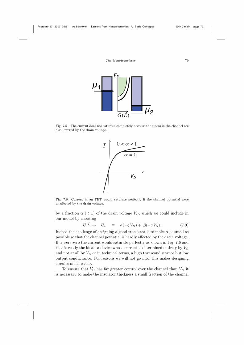
February 27, 2017 19:5 ws-book9x6 Lessons from Nanoelectronics: A. Basic Concepts 10440-main page 79
The Nanotransistor 79
E
μ1
G (E)μ2
Fig. 7.5 The current does not saturate completely because the states in the channel are
also lowered by the drain voltage.
I
VD
= 0
0 < < 1
Fig. 7.6 Current in an FET would saturate perfectly if the channel potential were
unaffected by the drain voltage.
by a fraction α (< 1) of the drain voltage VD, which we could include in
our model by choosing
U (2) → UL ≡ α(−q VD) + β(−q VG). (7.3)
Indeed the challenge of designing a good transistor is to make α as small as
possible so that the channel potential is hardly affected by the drain voltage.
If α were zero the current would saturate perfectly as shown in Fig. 7.6 and
that is really the ideal: a device whose current is determined entirely by VGand not at all by VD or in technical terms, a high transconductance but low
output conductance. For reasons we will not go into, this makes designing
circuits much easier.
To ensure that VG has far greater control over the channel than VD it
is necessary to make the insulator thickness a small fraction of the channel

February 27, 2017 19:5 ws-book9x6 Lessons from Nanoelectronics: A. Basic Concepts 10440-main page 80
80 Lessons from Nanoelectronics: A. Basic Concepts
length. This means that for a channel length of a few hundred atoms we
need an insulator that is only a few atoms thick in order to ensure a small
α. This thickness has to be precisely controlled since thinner insulators
would lead to unacceptably large leakage currents. We mentioned earlier
that today’s laptops have a billion transistors. What is even more amazing
is that each has an insulator whose thickness is precisely controlled down
to a few atoms!
7.3 Role of Charging
There is a second effect that leads to an increase in the saturation current
over what we get using Eq. (7.3) in Eq. (7.1). Under bias, the occupation
of the channel states is less than what it is at equilibrium. This is because
at equilibrium both contacts are trying to fill up the channel states, while
under bias only the source is trying to fill up the states while the drain is
trying to empty it. Since there are fewer electrons in the channel, it tends
to become positively charged and this will lower the states in the channel
as shown in Fig. 7.5, resulting in an increase in the current, even if the
electrostatics is perfect (α = 0) and the drain voltage has no effect on the
channel.
This effect can be captured within the point channel model (Eq. (7.1))
by writing the channel potential as
(A) U = UL + U0(N −N0) (7.4)
where UL is given by our previous expression in Eq. (7.3). The extra term
represents the change in the channel potential due to the change in the
number of electrons in the channel, N under non-equilibrium conditions
relative to the equilibrium number N0, U0 being the change in the channel
potential energy per electron. To use Eq. (7.4), we need expressions for N0
and N . N0 is the equilibrium number of channel electrons, which can be
calculated simply by filling up the density of states, D(E) according to the
equilibrium Fermi function f0(E).
(B1) N0 =
∫ +∞
−∞dE D(E − U) f0(E) (7.5)
while the number of electrons, N in the channel under non-equilibrium
conditions is given by
(B2) N =
∫ +∞
−∞dE D(E − U)
f1(E) + f2(E)
2(7.6)

February 27, 2017 19:5 ws-book9x6 Lessons from Nanoelectronics: A. Basic Concepts 10440-main page 81
The Nanotransistor 81
assuming that the channel is “equally” connected to both contacts. Note
that the calculation is now a little more intricate than what it would be if
U0 were zero. We now have to obtain a solution for U and N that satisfy
both Eqs. (7.4) and (7.6) simultaneously through an iterative procedure as
shown schematically in Fig. 7.7.
Once a self-consistent U has been obtained, the current is calculated
from Eq. (7.1), or an equivalent version that is sometimes more convenient
numerically and conceptually.
(C) I =1
q
∫ +∞
−∞dE G(E) (f1(E + U) − f2(E + U)). (7.7)
This simple point channel model often provides a good description of the
I-V characteristics as discussed in Rahman et al. (2003).
Guess U
Find N-N0(B1,B2)
Find new U(A)
Is new U almost same as the starting U ?
Update guess for U
YES
NO
Use U to calculate I
(C)
Fig. 7.7 Self-consistent procedure for calculating the channel potential U in pointchannel model.
Figure 7.9 shows the current versus voltage characteristic calculated
numerically (MATLAB code at end of chapter) assuming a 2D channel
with a parabolic dispersion relation for which the density of states is given
by (L: length, W : width, ϑ: unit step function)
D(E) = gmLW
2π~2ϑ(E − Ec). (7.8)
The numerical results are obtained using g = 2, m = 0.2× 9.1× 10−31 Kg,
β = 1, α = 0 and U0 = 0 or U0 = ∞ as indicated, with L = 1 µm, W = 1
µm assuming ballistic transport, so that
G(E) =q2
hM(E).

February 27, 2017 19:5 ws-book9x6 Lessons from Nanoelectronics: A. Basic Concepts 10440-main page 82
82 Lessons from Nanoelectronics: A. Basic Concepts
E
D(E)
μ0
Ec
Fig. 7.8 Density of states D(E) given in Eq. (7.8).
M(E) being the number of modes given by
M(E) = g2W
h
√2m(E − Ec)ϑ(E − Ec). (7.9)
The current-voltage characteristics in Fig. 7.9 has two distinct parts,
the initial linear increase followed by a saturation of the current. Although
these results were obtained numerically, both the slope and the saturation
current can be calculated analytically, especially if we make the low tem-
perature approximation that the Fermi functions change abruptly from 1
to 0 as the energy E crosses the electrochemical potential µ. Indeed we
used a kT of 5 meV instead of the usual 25 meV, so that the numerical
results would compare better with simple low temperature estimates.
U0 = 0, = 0
U0 , = 0
I2
I1
Fig. 7.9 Current-voltage characteristics calculated numerically using the self-consistent
point channel model shown in Fig. 7.7. MATLAB code included at end of chapter.

February 27, 2017 19:5 ws-book9x6 Lessons from Nanoelectronics: A. Basic Concepts 10440-main page 83
The Nanotransistor 83
E
μ1
G (E)μ2
There are two key points we wanted to illustrate with this example.
Firstly, the initial slope of the current-voltage characteristics is unaffected
by the charging energy. This slope defines the low bias conductance that
we have been discussing till we came to this chapter. The fact that it
remains unaffected is reassuring and justifies our not bringing up the role
of electrostatics earlier.
Secondly, the saturation current is strongly affected by the electrostatics
and changes by a factor of ∼ 2.8 from a model with zero charging energy
to one with a very large charging energy. This is because of the reason
mentioned at the beginning of this section. With U0 = 0, the channel
states remain fixed and the number of electrons N is equal to N0/2, since
f1 = 1 and f2 = 0 in the energy range of interest. With very large U0, to
avoid U0(N − N0) becoming excessive, N needs to be almost equal to N0
even though the states are only half-filled. This requires the states to move
down as sketched with a corresponding increase in the current.
7.3.1 Quantum capacitance
Related video lecture available at course website, Unit 2: L2.8.
We have generally focused on the shape of the current-voltage characteris-
tics obtained when a voltage is applied between the source and the drain,
which is a non-equilibrium problem. Let us take a brief detour to talk about
an equilibrium problem where charging can have a major effect. Suppose
the source and drain are held at the same potential while the gate voltage
VG is changed. How much does the number of electrons (N) change?
A positive gate voltage lowers the density of states D(E) resulting in

February 27, 2017 19:5 ws-book9x6 Lessons from Nanoelectronics: A. Basic Concepts 10440-main page 84
84 Lessons from Nanoelectronics: A. Basic Concepts
an increase in the number of electrons N . From Eq. (7.6)
N =
∫ +∞
−∞dE D(E) f0(E + U). (7.10)
Assuming that the electrochemical potential is located outside the band as
shown, it is usually permissible to use the Boltzmann approximation to the
Fermi function
f0(E) ≈ e−(E−µ)/kT
so that N = e−U/kT ×∫ +∞
−∞dE D(E) f0(E).
VG
U
D(E)
E
μ
To change the number of electrons by a factor of 10, we need a change in
the channel potential U by
kT ln (10) ≈ 60 meV.
To change the channel potential U by 60 meV, we need a gate voltage of at
least 60 mV, leading to an oft-quoted result that one needs a gate voltage
of at least 60 mV for every decade of change in N .
This discussion, however, is relevant only when the number of electrons
is relatively small. Once the electrochemical potential gets close to the
band, it is important to include the charging effect.
A positive gate voltage tries to lower the density of states as shown by
the solid line, which increases the number of electrons, but that in turn
causes the states to float up as indicated by the dashed line.

February 27, 2017 19:5 ws-book9x6 Lessons from Nanoelectronics: A. Basic Concepts 10440-main page 85
The Nanotransistor 85
D(E)
E
D(E)
E
μ
VG > 0 VG = 0
To determine the resulting N in general, one has to include this charging
effect. We can divide the problem into two parts, (1) the change in N due
to a change in the channel potential U , and (2) the change in U due to a
change in the gate voltage VG:
C = qdN
dVG= q
dN
(dU/− q)× dU
d(−qVG). (7.11)
The first term is the quantum capacitance which can be related to the
density of states starting from Eq. (7.8) as before (but not invoking the
Boltzmann approximation)
CQ = qdN
(dU/− q)
= q2
∫ +∞
−∞dE D(E)
(−∂f0
∂E
)= q2D0 (7.12)
whereD0 represents the averaged value of the density of statesD(E) around
E + U = µ, that is, around E = µ− U .
To evaluate the second term we write from Eq. (7.4), using Eq. (7.12),
dU
d(VG)=
dULd(VG)
+ U0dN
d(VG)=
dULd(VG)
− U0D0dU
d(VG).
Hence
dU
d(−qVG)=
1
1 + U0D0× dUL
d(−qVG). (7.13)
The second term represents the change in the potential UL due to a gate
voltage which ideally could approach one. But the actual change in the
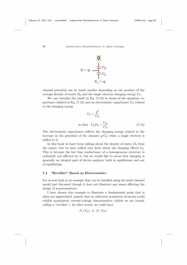
February 27, 2017 19:5 ws-book9x6 Lessons from Nanoelectronics: A. Basic Concepts 10440-main page 86
86 Lessons from Nanoelectronics: A. Basic Concepts
CE
CQU / −q
0
UL / −q
channel potential can be much smaller depending on the product of the
average density of states D0 and the single electron charging energy U0.
We can visualize the result in Eq. (7.13) in terms of the quantum ca-
pacitance defined in Eq. (7.12) and an electrostatic capacitance CE related
to the charging energy
U0 =q2
CE
so that U0D0 =CQCE
. (7.14)
The electrostatic capacitance reflects the charging energy related to the
increase in the potential of the channel q/CE when a single electron is
added to it.
In this book we have been talking about the density of states D0 from
the outset, but we have talked very little about the charging effects U0.
This is because the low bias conductance of a homogeneous structure is
ordinarily not affected by it, but we would like to stress that charging is
generally an integral part of device analysis, both in equilibrium and out
of equilibrium.
7.4 “Rectifier” Based on Electrostatics
Let us now look at an example that can be handled using the point channel
model just discussed though it does not illustrate any issues affecting the
design of nanotransistors.
I have chosen this example to illustrate a fundamental point that is
often not appreciated, namely that an otherwise symmetric structure could
exhibit asymmetric current-voltage characteristics (which we are loosely
calling a “rectifier”). In other words, we could have
I(+VD) 6= I(−VD)
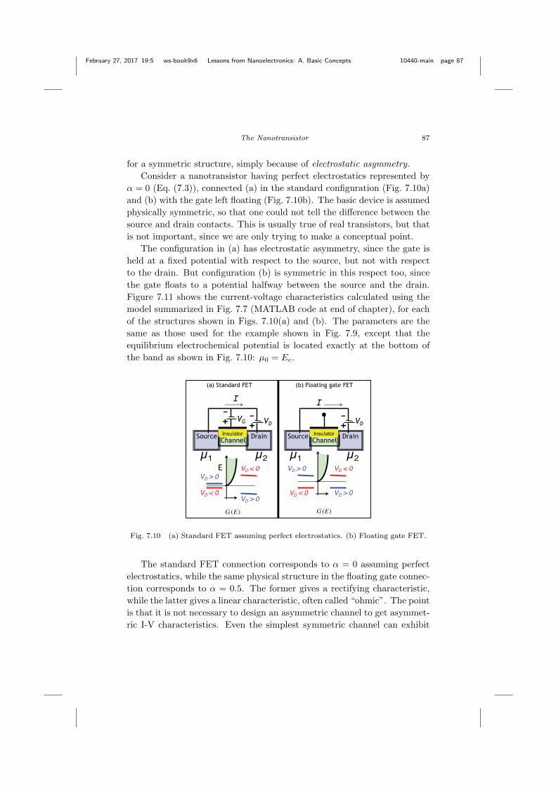
February 27, 2017 19:5 ws-book9x6 Lessons from Nanoelectronics: A. Basic Concepts 10440-main page 87
The Nanotransistor 87
for a symmetric structure, simply because of electrostatic asymmetry.
Consider a nanotransistor having perfect electrostatics represented by
α = 0 (Eq. (7.3)), connected (a) in the standard configuration (Fig. 7.10a)
and (b) with the gate left floating (Fig. 7.10b). The basic device is assumed
physically symmetric, so that one could not tell the difference between the
source and drain contacts. This is usually true of real transistors, but that
is not important, since we are only trying to make a conceptual point.
The configuration in (a) has electrostatic asymmetry, since the gate is
held at a fixed potential with respect to the source, but not with respect
to the drain. But configuration (b) is symmetric in this respect too, since
the gate floats to a potential halfway between the source and the drain.
Figure 7.11 shows the current-voltage characteristics calculated using the
model summarized in Fig. 7.7 (MATLAB code at end of chapter), for each
of the structures shown in Figs. 7.10(a) and (b). The parameters are the
same as those used for the example shown in Fig. 7.9, except that the
equilibrium electrochemical potential is located exactly at the bottom of
the band as shown in Fig. 7.10: µ0 = Ec.
E
VD > 0
G (E)
VD > 0
VD < 0
VD < 0
ChannelSource Drain
VG VD
I
μ2μ1 E
VD > 0
G (E)
VD > 0
VD < 0
VD < 0
μ2μ1
ChannelSource Drain
VD
I
(b) Floating gate FET(a) Standard FET
-+ -
+-+
Fig. 7.10 (a) Standard FET assuming perfect electrostatics. (b) Floating gate FET.
The standard FET connection corresponds to α = 0 assuming perfect
electrostatics, while the same physical structure in the floating gate connec-
tion corresponds to α = 0.5. The former gives a rectifying characteristic,
while the latter gives a linear characteristic, often called “ohmic”. The point
is that it is not necessary to design an asymmetric channel to get asymmet-
ric I-V characteristics. Even the simplest symmetric channel can exhibit

February 27, 2017 19:5 ws-book9x6 Lessons from Nanoelectronics: A. Basic Concepts 10440-main page 88
88 Lessons from Nanoelectronics: A. Basic Concepts
(b) Floating gate FET ,
= 0.5(a) S ard FET ,
with = 0
Fig. 7.11 Current-voltage characteristics obtained from the point channel model corre-
sponding to the configurations shown in Fig. 7.10. MATLAB code included at end ofchapter.
non-symmetric I(VD) characteristic if the electrostatics is asymmetric.
Note also that the linear conductance given by the slope dI/dV around
V = 0 is unaffected by our choice of α and can be predicted without
any reference to the electrostatics, even though the overall shape obviously
cannot.
7.5 Extended Channel Model
The point channel elastic model that we have described (Eqs. (7.1) and
(7.4)) integrates our elastic resistor with a simple electrostatic model for
the channel potential U/q, allowing it to capture some of the high bias
physics that the pure elastic resistor misses. Let us now talk briefly about
some of the things we are still missing.
The point channel model ignores the electric field in the channel and
assumes that the density of states D(E) stays the same from source to
drain. In the real structure, however, the electric field lowers the states at
the drain end relative to the source as sketched here. Doesn’t this change
the current?
For an elastic resistor one could argue that the additional states with
the slanted (rather than horizontal) shading are not really available for con-
duction since (in an elastic resistor) every energy represents an independent
energy channel and can only conduct if it connects all the way from the
source to the drain.
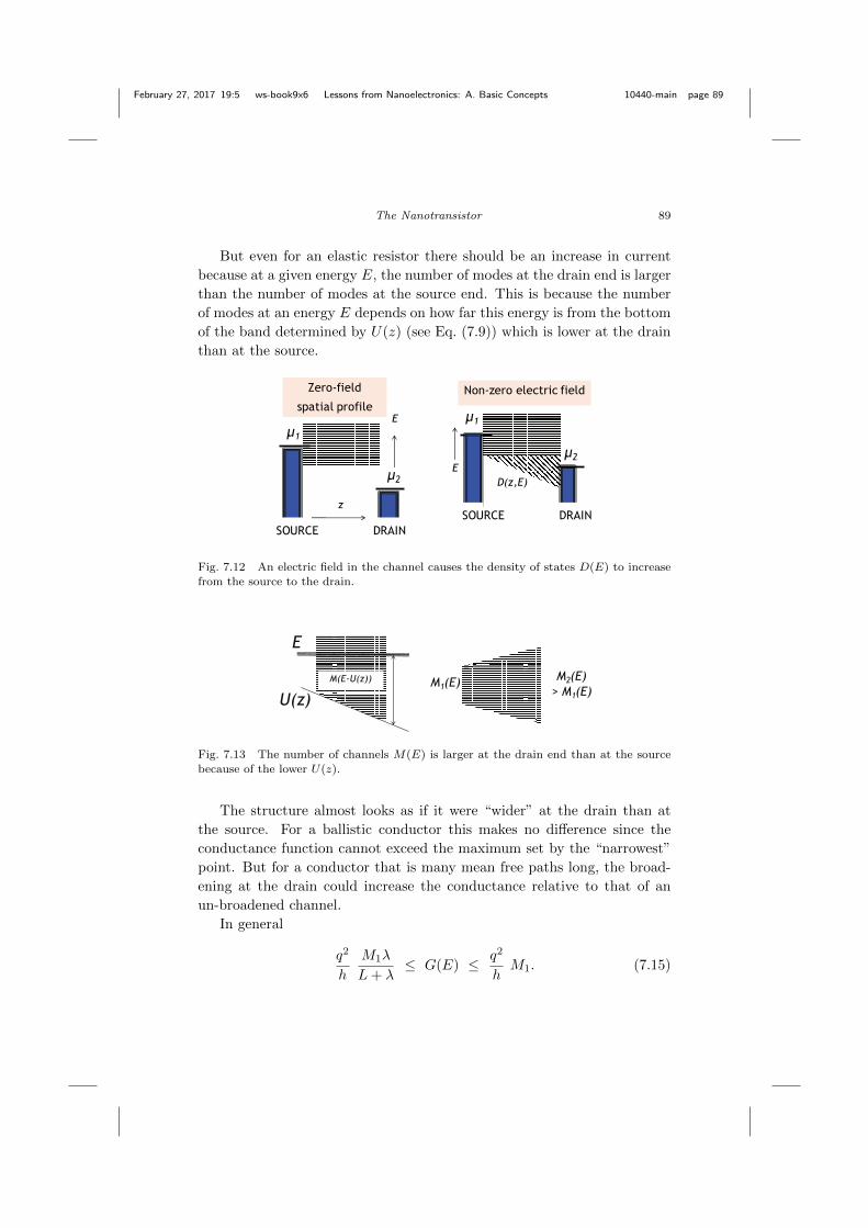
February 27, 2017 19:5 ws-book9x6 Lessons from Nanoelectronics: A. Basic Concepts 10440-main page 89
The Nanotransistor 89
But even for an elastic resistor there should be an increase in current
because at a given energy E, the number of modes at the drain end is larger
than the number of modes at the source end. This is because the number
of modes at an energy E depends on how far this energy is from the bottom
of the band determined by U(z) (see Eq. (7.9)) which is lower at the drain
than at the source.
µ1
µ2
Non-zero electric field
E
SOURCE DRAIN
D(z,E)
Zero-field
spatial profileE
z
SOURCE DRAIN
µ1
µ2
Fig. 7.12 An electric field in the channel causes the density of states D(E) to increase
from the source to the drain.
M(E-U(z))
U(z)
E
M1(E) M2(E)> M1(E)
Fig. 7.13 The number of channels M(E) is larger at the drain end than at the source
because of the lower U(z).
The structure almost looks as if it were “wider” at the drain than at
the source. For a ballistic conductor this makes no difference since the
conductance function cannot exceed the maximum set by the “narrowest”
point. But for a conductor that is many mean free paths long, the broad-
ening at the drain could increase the conductance relative to that of an
un-broadened channel.
In general
q2
h
M1λ
L+ λ≤ G(E) ≤ q2
hM1. (7.15)
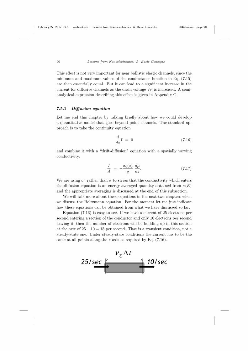
February 27, 2017 19:5 ws-book9x6 Lessons from Nanoelectronics: A. Basic Concepts 10440-main page 90
90 Lessons from Nanoelectronics: A. Basic Concepts
This effect is not very important for near ballistic elastic channels, since the
minimum and maximum values of the conductance function in Eq. (7.15)
are then essentially equal. But it can lead to a significant increase in the
current for diffusive channels as the drain voltage VD is increased. A semi-
analytical expression describing this effect is given in Appendix C.
7.5.1 Diffusion equation
Let me end this chapter by talking briefly about how we could develop
a quantitative model that goes beyond point channels. The standard ap-
proach is to take the continuity equation
d
dzI = 0 (7.16)
and combine it with a “drift-diffusion” equation with a spatially varying
conductivity:
I
A= −σ0(z)
q
dµ
dz. (7.17)
We are using σ0 rather than σ to stress that the conductivity which enters
the diffusion equation is an energy-averaged quantity obtained from σ(E)
and the appropriate averaging is discussed at the end of this subsection.
We will talk more about these equations in the next two chapters when
we discuss the Boltzmann equation. For the moment let me just indicate
how these equations can be obtained from what we have discussed so far.
Equation (7.16) is easy to see. If we have a current of 25 electrons per
second entering a section of the conductor and only 10 electrons per second
leaving it, then the number of electrons will be building up in this section
at the rate of 25− 10 = 15 per second. That is a transient condition, not a
steady-state one. Under steady-state conditions the current has to be the
same at all points along the z-axis as required by Eq. (7.16).
!z ! t
10/sec25/sec

February 27, 2017 19:5 ws-book9x6 Lessons from Nanoelectronics: A. Basic Concepts 10440-main page 91
The Nanotransistor 91
μ2μ1
f (z) f (z + z)I(z)
To obtain Eq. (7.17) we view a long conductor as a series of elastic
resistors as discussed in Section 3.3. Using Eq. (3.3) we can write the
current I(z) in a section of the conductor as
I(z) =1
q
∫ +∞
−∞dE G(E) (f(z, E) − f(z + 4z, E)).
From Eq. (4.5a) we could write
1
G(E)= ρ
4z + λ
A
but the point to note is that part of this resistance represents the interface
resistance, which should not be included since there are no actual interfaces
except at the very ends. Omitting the interface resistance we can write
(Note: σ = 1/ρ)
G(E) =σA
4z.
Combining this with our usual linear expansion for small potential differ-
ences from Eq. (2.10)
(f(z, E) − f(z + 4z, E)) ≡(−∂f0
∂E
)(µ(z, E) − µ(z + 4z, E))
and defining the conductivity as the thermal average of σ(E) (Eq. (6.6)),
we obtain
I(z) =1
q
σ0A
4z(µ(z) − µ(z + 4z)).
Letting ∆→ 0, we obtain Eq. (7.17).
What do we use for the conductivity, σ0? Our old expression
σ0 =
∫ +∞
−∞dE σ(E)
(− ∂f∂E
)E=µ0
(same as Eq. (6.6))
involved an energy average of over an energy window of a few kT around
E = µ0.

February 27, 2017 19:5 ws-book9x6 Lessons from Nanoelectronics: A. Basic Concepts 10440-main page 92
92 Lessons from Nanoelectronics: A. Basic Concepts
U(z)
!(z)
!-U
The spatially varying U(z) shifts the available energy states in energy,
so that one now has to look at the energy window around E = µ(z)−U(z)
suggesting that we replace Eq. (6.6) with
σ0 =
∫ +∞
−∞dE σ(E)
(− ∂f∂E
)E=µ(z)−U(z)
. (7.18)
7.5.2 Charging: Self-consistent solution
Note that to use Eq. (7.18) we have to determine µ(z)− U(z) from a self-
consistent solution the Poisson equation (ε: Permittivity, n0, n: electron
density per unit volume at equilibrium and out of equilibrium)
(A′)d
dz
(εdU
dz
)= q2 (n − n0). (7.19)
The electron density per unit length entering the Poisson equation is calcu-
lated by filling up the density of states (per unit length) shifted by the local
potential U(z), according to the local electrochemical potential, so that we
can write
(B1′) n(z) ≡∫ +∞
−∞dE
D(E − U(z))
L
1
1 + exp
(E − µ(z)
kT
) (7.20a)
(B2′) n0 =
∫ +∞
−∞dE
D(E)
L
1
1 + exp
(E − µ0
kT
) . (7.20b)
Solving Eq. (7.20) self-consistently with the Poisson equation (Eq. (7.19))
is indeed the standard approach to obtaining the correct µ(z) and U(z),
which can then be used to find the current from Eq. (7.17). We could view
this procedure as the extended channel version of the point channel model
in Fig. 7.7 as shown in Fig. 7.14.

February 27, 2017 19:5 ws-book9x6 Lessons from Nanoelectronics: A. Basic Concepts 10440-main page 93
The Nanotransistor 93
Guess U(z)
Find n(z)-n0(z)(B1’,B2’)
Find new U(z)(A’)
Is new U almost same as the starting U ?
Update guess for U
YES
NO
Use U to calculate I
(C’)
Fig. 7.14 Extended channel version of the point channel model in Fig. 7.7.
Note that this whole approach is based on the assumption of a local elec-
trochemical potential µ(z) appearing in Eq. (7.20a). In general, electron
distributions can deviate so badly from Fermi functions that an electro-
chemical potential may not be adequate and one needs the full semiclassical
formalism based on the Boltzmann Transport Equation (BTE) which we
discuss in Chapter 9.
Much progress has been made in this direction but full-fledged BTE-
based simulation is time-consuming and the drift-diffusion equation based
on the concept of a local potential µ(z) continues to be the “bread and
butter” of device modeling. But the diffusion equation has been around a
long time. What are we adding to it? It is the extra interface resistance
that changes
G(E) =σA
Lto
σA
L + λ.
In the next chapter we will show that this result follows from the diffusion
equation if the boundary conditions are modified appropriately and to jus-
tify this modified boundary condition requires a deeper discussion of the
meaning of the electrochemical potential on a nanometer scale.
7.6 MATLAB Codes for Figs. 7.9 and 7.11
These codes are included here mainly for their pedagogical value.
Soft copies are available through our website
https://nanohub.org/groups/lnebook
% Saturation current

February 27, 2017 19:5 ws-book9x6 Lessons from Nanoelectronics: A. Basic Concepts 10440-main page 94
94 Lessons from Nanoelectronics: A. Basic Concepts
clear all
% Constants
hbar=1.06e-34;q=1.6e-19;
%Parameters
m=0.2*9.1e-31;g=2;ep=4*8.854e-12;
% mass, degeneracy factor, permittivity
kT=0.005;mu0=0.05;
% Thermal energy, equilibrium electrochemical potential
W=1e-6;L=1e-6;tox=2e-9;% dimensions
% Energy grid
dE=0.00001;E=[0:dE:2];NE=size(E,2);
D=(g*W*L*q*m/2/pi/hbar/hbar).*ones(1,NE);
% Density of states
M=(g*2*W/2/pi/hbar).*sqrt(2*m*q*E);% Number of modes
f0=1./(1+exp((E-mu0)./kT));
% Equilibrium Fermi function
N0=sum(dE*D.*f0);% Equilibrium electron number
U0=0*q*tox/ep/L/W;% Charging energy
alpha=0.05;% Drain induced barrier lowering
% I-V characteristics
ii=1;dV=0.01;for V=1e-3:dV:0.5
UL=-alpha*V;ii
change=100;U=UL;
% Self-consistent loop
while change>1e-6
f1=1./(1+exp((E-mu0+U)./kT));
f2=1./(1+exp((E-mu0+U+V)./kT));
f=(f1+f2)./2;
N=sum(dE*D.*f);% Electron number
Unew=UL+U0*(N-N0);% Self-consistent potential
change=abs(U-Unew);
U=U+0.05*(Unew-U);
end

February 27, 2017 19:5 ws-book9x6 Lessons from Nanoelectronics: A. Basic Concepts 10440-main page 95
The Nanotransistor 95
curr(ii)=(q*q*dE/2/pi/hbar)*sum(M.*(f1-f2));
volt(ii)=V;Uscf(ii)=U;ns(ii)=N/W/L;ii=ii+1;
end
current=q*g*(4/3)*W*sqrt(2*m*q*mu0)*q*mu0/
4/pi/pi/hbar/hbar;
max(curr)/current
h=plot(volt,curr,’r’);
%h=plot(volt,curr,’r+’);
%h=plot(volt,Uscf,’r’);
%h=plot(volt,ns,’r’);
set(h,’linewidth’,[3.0])
set(gca,’Fontsize’,[40])
xlabel(’ Voltage (V_D) ---> ’);
ylabel(’ Current (A) ---> ’);
% Electrostatic rectifier
clear all
% Constants
hbar=1.06e-34;q=1.6e-19;
%Parameters
m=0.2*9.1e-31;g=2;ep=4*8.854e-12;
% mass, degeneracy factor, permittivity
kT=0.025;mu0=0*0.05;
% Thermal energy, equilibrium electrochemicalpotential
W=1e-6;L=1e-6;tox=2e-9;% dimensions
% Energy grid
dE=0.0001;E=[0:dE:2];NE=size(E,2);
D=(g*W*L*q*m/2/pi/hbar/hbar).*ones(1,NE);
% Density of states
M=(g*2*W/2/pi/hbar).*sqrt(2*m*q*E);% Number of modes
f0=1./(1+exp((E-mu0)./kT));
% Equilibrium Fermi function

February 27, 2017 19:5 ws-book9x6 Lessons from Nanoelectronics: A. Basic Concepts 10440-main page 96
96 Lessons from Nanoelectronics: A. Basic Concepts
N0=sum(dE*D.*f0);% Equilibrium electron number
U0=0*q*tox/ep/L/W;% Charging energy
alpha=0;% Drain induced barrier lowering
% I-V characteristics
ii=1;dV=0.01;for V=-0.1:dV:0.1
UL=-alpha*V;ii
change=100;U=UL;
% Self-consistent loop
while change>1e-6
f1=1./(1+exp((E-mu0+U)./kT));
f2=1./(1+exp((E-mu0+U+V)./kT));
f=(f1+f2)./2;
N=sum(dE*D.*f);% Electron number
Unew=UL+U0*(N-N0);% Self-consistent potential
change=abs(U-Unew);
U=U+0.05*(Unew-U);
end
curr(ii)=(g*q*q*dE/2/pi/hbar)*sum(M.*(f1-f2));
volt(ii)=V;Uscf(ii)=U;ns(ii)=N/W/L;ii=ii+1;
end
h=plot(volt,curr,’r’);
%h=plot(volt,Uscf,’r’);
%h=plot(volt,ns,’r’);
set(h,’linewidth’,[3.0])
set(gca,’Fontsize’,[40])
xlabel(’ Voltage (V_D) ---> ’);
ylabel(’ Current (A) ---> ’);

February 27, 2017 19:5 ws-book9x6 Lessons from Nanoelectronics: A. Basic Concepts 10440-main page 97
PART 3
What and Where is the Voltage Drop
97

February 27, 2017 19:5 ws-book9x6 Lessons from Nanoelectronics: A. Basic Concepts 10440-main page 98
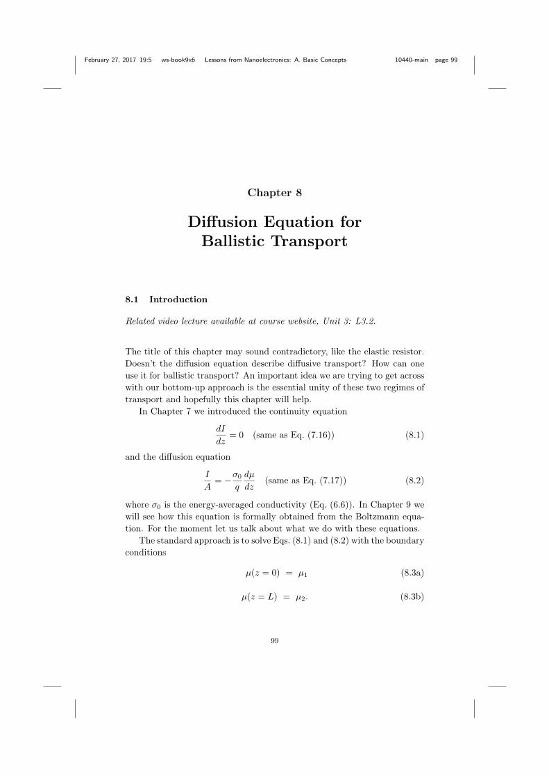
February 27, 2017 19:5 ws-book9x6 Lessons from Nanoelectronics: A. Basic Concepts 10440-main page 99
Chapter 8
Diffusion Equation forBallistic Transport
8.1 Introduction
Related video lecture available at course website, Unit 3: L3.2.
The title of this chapter may sound contradictory, like the elastic resistor.
Doesn’t the diffusion equation describe diffusive transport? How can one
use it for ballistic transport? An important idea we are trying to get across
with our bottom-up approach is the essential unity of these two regimes of
transport and hopefully this chapter will help.
In Chapter 7 we introduced the continuity equation
dI
dz= 0 (same as Eq. (7.16)) (8.1)
and the diffusion equation
I
A= −σ0
q
dµ
dz(same as Eq. (7.17)) (8.2)
where σ0 is the energy-averaged conductivity (Eq. (6.6)). In Chapter 9 we
will see how this equation is formally obtained from the Boltzmann equa-
tion. For the moment let us talk about what we do with these equations.
The standard approach is to solve Eqs. (8.1) and (8.2) with the boundary
conditions
µ(z = 0) = µ1 (8.3a)
µ(z = L) = µ2. (8.3b)
99

February 27, 2017 19:5 ws-book9x6 Lessons from Nanoelectronics: A. Basic Concepts 10440-main page 100
100 Lessons from Nanoelectronics: A. Basic Concepts
z = 0 z = L
!2
!1
Source Drain!"#$$%&
!"#$%&'()*&&#(%
!'$(%$)*'$#&!+,,%$)
I
Fig. 8.1 Solution to Eqs. (8.1) and (8.2) with the boundary conditions in Eq. (8.3). Notethat we are using I to represent the electron current as explained earlier (see Fig. 3.3).
It is easy to see that the linear solution sketched in Fig. 8.1 meets
the boundary conditions in Eq. (8.3) and at the same time satisfies both
Eqs. (8.1) and (8.2) since a linear µ(z) has a constant slope given by
dµ
dz= − µ1 − µ2
L
so that from Eq. (8.2) we have a constant current with dI/dz = 0:
I =σ0A
q
µ1 − µ2
L.
Note that µ1 − µ2 = qV (Eq. (2.1)), so that
I =σ0A
LV (8.4)
which is the standard expression and not the generalized one we have been
discussing
I =σ0A
L+ λV (8.5)
that includes ballistic channels as well. Can we obtain this result (Eq. (8.5))
from the diffusion equation (Eq. (8.2))?
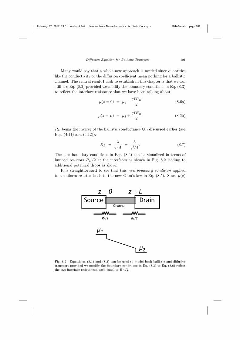
February 27, 2017 19:5 ws-book9x6 Lessons from Nanoelectronics: A. Basic Concepts 10440-main page 101
Diffusion Equation for Ballistic Transport 101
Many would say that a whole new approach is needed since quantities
like the conductivity or the diffusion coefficient mean nothing for a ballistic
channel. The central result I wish to establish in this chapter is that we can
still use Eq. (8.2) provided we modify the boundary conditions in Eq. (8.3)
to reflect the interface resistance that we have been talking about:
µ(z = 0) = µ1 −qIRB
2(8.6a)
µ(z = L) = µ2 +qIRB
2(8.6b)
RB being the inverse of the ballistic conductance GB discussed earlier (see
Eqs. (4.11) and (4.12)):
RB =λ
σ0A=
h
q2M. (8.7)
The new boundary conditions in Eqs. (8.6) can be visualized in terms of
lumped resistors RB/2 at the interfaces as shown in Fig. 8.2 leading to
additional potential drops as shown.
It is straightforward to see that this new boundary condition applied
to a uniform resistor leads to the new Ohm’s law in Eq. (8.5). Since µ(z)
z = 0 z = L
µ2
µ1
Source Drain
RB/2 RB/2
Fig. 8.2 Equations. (8.1) and (8.2) can be used to model both ballistic and diffusivetransport provided we modify the boundary conditions in Eq. (8.3) to Eq. (8.6) reflect
the two interface resistances, each equal to RB/2.

February 27, 2017 19:5 ws-book9x6 Lessons from Nanoelectronics: A. Basic Concepts 10440-main page 102
102 Lessons from Nanoelectronics: A. Basic Concepts
varies linearly from z = 0 to z = L, the current is obtained from Eq. (8.2)
I =σ0A
q
µ(0)− µ(L)
L.
Using Eqs. (8.6)
I =σ0A
q
(µ1 − µ2
L− qIRB
L
).
Since, σ0ARB = λ (Eq. (8.7)),
I
(1 +
λ
L
)=σ0A
q
(µ1 − µ2
L
).
Noting that µ1 − µ2 = qV (Eq. (2.1)) this yields Eq. (8.5).
But how do we justify this new boundary condition (Eqs. (8.6))? It
follows from the new Ohm’s law (Eq. (8.5)) if we assume that the ex-
tra resistance corresponding to L = 0 is equally divided between the two
interfaces. For a better justification, we need to introduce two different
electrochemical potentials µ+ and µ− for electrons moving along +z and
−z respectively. In previous chapters we talked about electrochemical po-
tentials inside the contacts which are large regions that always remain close
to equilibrium and hence are described by Fermi functions (see Eqs. (2.7))
with well-defined electrochemical potentials.
By contrast in this chapter we are using µ(z) to represent quantities
inside the out-of-equilibrium channel, where it is at best an approximate
concept since the electron distribution among the available states need not
follow a Fermi function. Even if it does, electronic states carrying current
along +z must be occupied differently from those carrying current along
−z, or else there would be no net current. This difference in occupation
is reflected in different electrochemical potentials µ+ and µ− and we will
show that the current is proportional to the difference (see Eq. (8.23) in
Section 8.3)
I =q
hM(µ+(z)− µ−(z)) (8.8)
which can also be rewritten in the form
I =1
qRB(µ+(z)− µ−(z)) (8.9)
=σ0A
qλ(µ+(z)− µ−(z)) (8.10)
using Eq. (4.4b). The correct boundary conditions for µ+ and µ− are
µ+(z = 0) = µ1 (8.11)
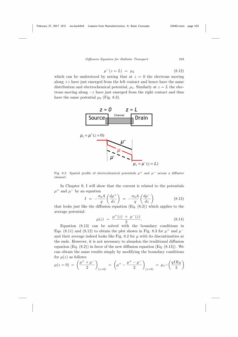
February 27, 2017 19:5 ws-book9x6 Lessons from Nanoelectronics: A. Basic Concepts 10440-main page 103
Diffusion Equation for Ballistic Transport 103
µ−(z = L) = µ2 (8.12)
which can be understood by noting that at z = 0 the electrons moving
along +z have just emerged from the left contact and hence have the same
distribution and electrochemical potential, µ1. Similarly at z = L the elec-
trons moving along −z have just emerged from the right contact and thus
have the same potential µ2 (Fig. 8.3).
μ2 = μ (z = L)
μ1 = μ+ (z = 0)
µ+
µ-
µ
z = 0 z = LSource Drain
Fig. 8.3 Spatial profile of electrochemical potentials µ+ and µ− across a diffusivechannel.
In Chapter 9, I will show that the current is related to the potentials
µ+ and µ− by an equation
I = −σ0A
q
(dµ+
dz
)= −σ0A
q
(dµ−
dz
)(8.13)
that looks just like the diffusion equation (Eq. (8.2)) which applies to the
average potential:
µ(z) =µ+(z) + µ−(z)
2. (8.14)
Equation (8.13) can be solved with the boundary conditions in
Eqs. (8.11) and (8.12) to obtain the plot shown in Fig. 8.3 for µ+ and µ−
and their average indeed looks like Fig. 8.2 for µ with its discontinuities at
the ends. However, it is not necessary to abandon the traditional diffusion
equation (Eq. (8.2)) in favor of the new diffusion equation (Eq. (8.13)). We
can obtain the same results simply by modifying the boundary conditions
for µ(z) as follows:
µ(z = 0) =
(µ+ + µ−
2
)(z=0)
=
(µ+ − µ+ − µ−
2
)(z=0)
= µ1−(qIRB
2
)

February 27, 2017 19:5 ws-book9x6 Lessons from Nanoelectronics: A. Basic Concepts 10440-main page 104
104 Lessons from Nanoelectronics: A. Basic Concepts
making use of Eqs. (8.9) and (8.11). Similarly using Eqs. (8.9) and (8.12)
µ(z = L) =
(µ− +
µ+ − µ−
2
)(z=L)
= µ2 +
(qIRB
2
).
These are exactly the new boundary conditions for the standard diffusion
equation that we mentioned earlier (Eqs. (8.6)).
8.1.1 A disclaimer
The simple description provided above is an approximate one designed to
convey a qualitative physical picture. The out-of-equilibrium occupation
of different states is in general quite complicated and cannot necessarily be
captured with just two potentials µ+ and µ−, even for an elastic resistor
at low bias. Indeed the rest of this chapter is intended to give the reader a
feeling for the underlying concepts and issues. In the next chapter we intro-
duce the Boltzmann equation which is the gold standard for semiclassical
transport against which all approximate pictures have to be measured. In
subsequent chapters (Chapters 10, 11 and 12) we will discuss different as-
pects related to the difficult but very important concept of electrochemical
potentials or quasi-Fermi levels under non-equilibrium conditions.
8.2 Electrochemical Potentials Out of Equilibrium
Related video lecture available at course website, Unit 3: L3.3.
As I mentioned earlier, it is conceptually straightforward to talk about
electrochemical potentials inside the contacts which are large regions that
always remain close to equilibrium and hence are described by Fermi func-
tions (see Eq. (2.7)) with well-defined electrochemical potentials. But in an
out-of-equilibrium channel, the electron distribution among the available
states need not follow a Fermi function. In general one has to solve a full-
fledged transport equation like the semiclassical Boltzmann equation to be
introduced in the next chapter which allows us to calculate the full occupa-
tion factors f(z;E). More generally for quantum transport one can use the
non-equilibrium Green’s function (NEGF) formalism discussed in Part B
to solve for the quantum version of f(z;E). Can we really represent these
distribution functions using electrochemical potentials µ+(z) and µ−(z)?
Interestingly for a perfectly ballistic channel with good contacts, such
a representation in terms of µ+(z) and µ−(z) is exact and not just an

February 27, 2017 19:5 ws-book9x6 Lessons from Nanoelectronics: A. Basic Concepts 10440-main page 105
Diffusion Equation for Ballistic Transport 105
approximation. All drainbound electrons (traveling along +z, see Fig. 8.4)
are distributed according to the source contact with µ+ = µ1:
f+(z;E) = f1(E) ≡ 1
1 + exp
(E − µ1
kT
) (8.15)
while all sourcebound electrons (traveling along −z) are distributed accord-
ing to the drain contact with µ− = µ2:
f−(z;E) = f2(E) ≡ 1
1 + exp
(E − µ2
kT
) . (8.16)
This is justified by noting that the drainbound channels from the source
are filled only with electrons originating in the source and so these channels
remain in equilibrium with the source with a distribution function f1(E).
Similarly the sourcebound channels from the drain are in equilibrium with
the drain with a distribution function f2(E).
Suppose at some energy f1(E) = 1 and f2(E) = 0 so that there are lots
of electrons waiting to get out of the source, but none in the drain. We
would then expect the drainbound lanes of the electronic highway to be
completely full (“bumper-to-bumper traffic”), while the sourcebound lanes
would all be empty as shown below in Fig. 8.4.
0
f+
L
f1= 1
f2=0f-
z = 0 z = LSource Drain
Fig. 8.4 Spatial profile of the occupation factors f+ and f− across a ballistic channel.
Of course this assumes that electrons do not turn around either along the
way or at the ends. This means ballistic channels with good contacts where
there are so many channels available that electrons can exit smoothly with
a very low probability of turning around. If we either have bad contacts or
diffusive channels, the solution in Eqs. (8.15) and (8.16) wouldn’t work.
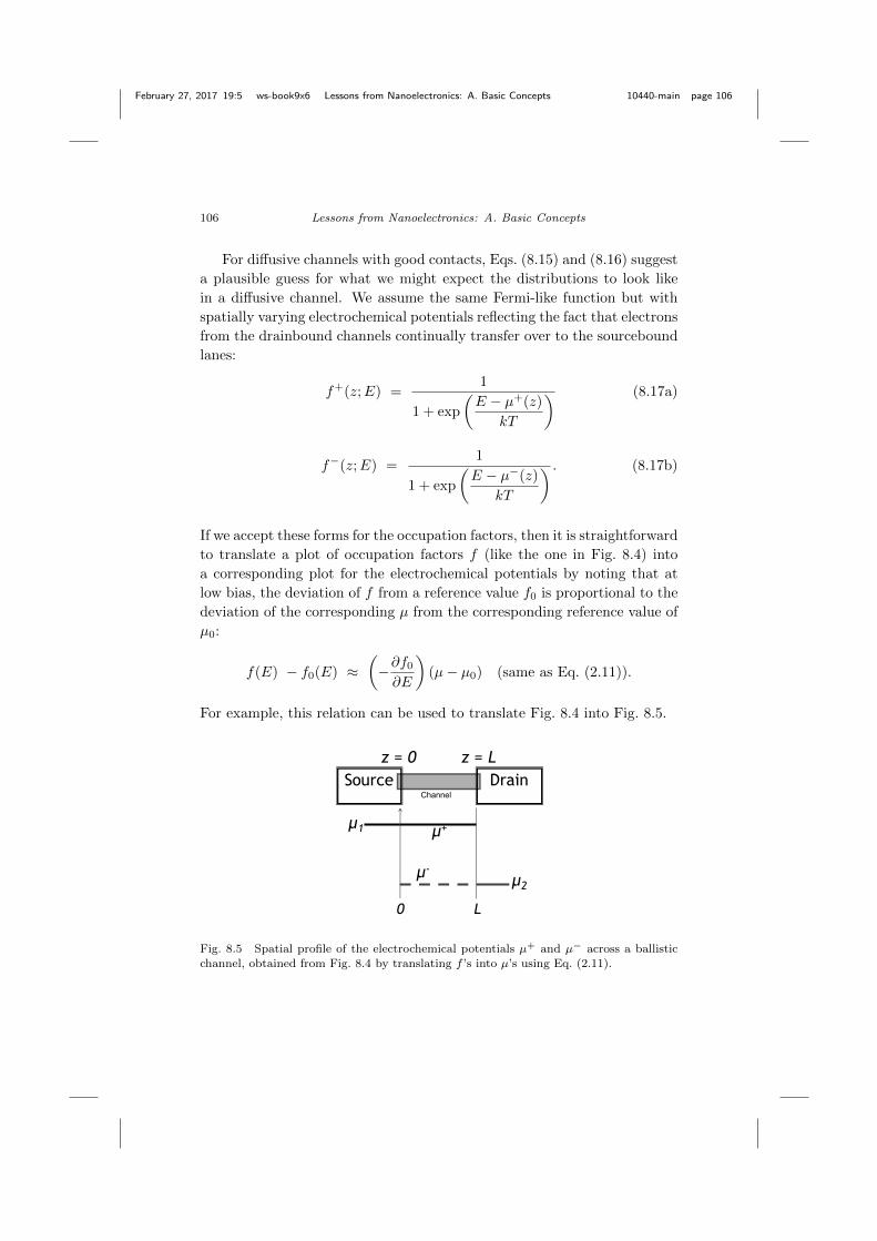
February 27, 2017 19:5 ws-book9x6 Lessons from Nanoelectronics: A. Basic Concepts 10440-main page 106
106 Lessons from Nanoelectronics: A. Basic Concepts
For diffusive channels with good contacts, Eqs. (8.15) and (8.16) suggest
a plausible guess for what we might expect the distributions to look like
in a diffusive channel. We assume the same Fermi-like function but with
spatially varying electrochemical potentials reflecting the fact that electrons
from the drainbound channels continually transfer over to the sourcebound
lanes:
f+(z;E) =1
1 + exp
(E − µ+(z)
kT
) (8.17a)
f−(z;E) =1
1 + exp
(E − µ−(z)
kT
) . (8.17b)
If we accept these forms for the occupation factors, then it is straightforward
to translate a plot of occupation factors f (like the one in Fig. 8.4) into
a corresponding plot for the electrochemical potentials by noting that at
low bias, the deviation of f from a reference value f0 is proportional to the
deviation of the corresponding µ from the corresponding reference value of
µ0:
f(E) − f0(E) ≈(−∂f0
∂E
)(µ− µ0) (same as Eq. (2.11)).
For example, this relation can be used to translate Fig. 8.4 into Fig. 8.5.
0
µ+
L
µ1
µ2µ-
z = 0 z = LSource Drain
Fig. 8.5 Spatial profile of the electrochemical potentials µ+ and µ− across a ballistic
channel, obtained from Fig. 8.4 by translating f ’s into µ’s using Eq. (2.11).

February 27, 2017 19:5 ws-book9x6 Lessons from Nanoelectronics: A. Basic Concepts 10440-main page 107
Diffusion Equation for Ballistic Transport 107
Note that Eq. (8.17) is a “guess” that in general requires careful scrutiny
and justification, if we are interested in quantitative results. For example,
in an elastic resistor, every energy is independent and in general each one
could exhibit a different spatial variation in the potential if the mean free
path is energy-dependent. This means we should write the potentials as
µ±(z;E). We will talk further about similar issues in the next chapter when
we discuss the Boltzmann equation.
8.3 Current from QFL’s
Related video lecture available at course website, Unit 3: L3.4.
Let me finish up this chapter by establishing a key result that stated earlier
without proof in Eq. (8.8). Usually we talk about the net current I which
can be expressed as the difference between the drainbound flux I+ and the
sourcebound flux I−:
I(z) = I+(z) − I−(z). (8.18)
The current I+ equals the amount of charge exiting from the right per unit
time. In a time ∆t, all the charge in a length vz∆t exits, so that
I+ = q × (Electrons per unit length)× vz.
z t
I+
The number of electrons per unit length is equal to half the density of
states (since only half the states carry current to the right) per unit length,
D(E)/2L, times the fraction f+ of occupied states, so that
I+(z;E) = qD(E)
2Lu(E)︸ ︷︷ ︸
M(E)/h
f+(z;E).
February 27, 2017 19:5 ws-book9x6 Lessons from Nanoelectronics: A. Basic Concepts 10440-main page 108
108 Lessons from Nanoelectronics: A. Basic Concepts
Here u is the average vz as defined in Eq. (4.8) and making use of the
definition of the number of channels M from Eq. (4.13) we have
I+(z;E) = qM(E)
hf+(z;E). (8.19)
Similarly
I−(z;E) = qM(E)
hf−(z;E). (8.20)
This allows us to write the current from Eq. (8.18)
I(z) =
∫ +∞
−∞dE(I+(z;E) − I−(z;E))
=q
h
∫ +∞
−∞dE(f+(z;E) − f−(z;E))M(E). (8.21)
Once again, to get from distribution functions f± to electrochemical po-
tentials µ±, we make use of the low bias result (Eq. (2.11) to write
f+(z;E) − f−(z;E) =
(−∂f0
∂E
)(µ+(z) − µ−(z)) (8.22)
and obtain Eq. (8.8)
I(z) =q
h(µ+(z) − µ−(z))
∫ +∞
−∞dE
(−∂f0
∂E
)M(E)︸ ︷︷ ︸
≡M
(8.23)
provided we identify M with the thermally averaged M(E) as indicated in
Eq. (8.23).
February 27, 2017 19:5 ws-book9x6 Lessons from Nanoelectronics: A. Basic Concepts 10440-main page 109
Chapter 9
Boltzmann Equation
Related video lecture available at course website, Unit 3: L3.8.
9.1 Introduction
Interestingly so far in this book we have hardly ever mentioned the electric
field, in contrast to most treatments of electronic transport which start by
considering the electric field induced force as the driving term. It may seem
paradoxical that we could obtain the conductivity without ever mentioning
the electric field! Electric fields are typically visualized as the gradient
of an electrostatic potential U/q. By contrast, we have been using the
electrochemical potential µ as the basis for our discussions. It is important
to recognize the difference between the two “potentials”:
µ︸︷︷︸Electrochemical
= (µ − U)︸ ︷︷ ︸Chemical
+ U︸︷︷︸Electrostatic
(9.1)
µ is a measure of the energy up to which the states are filled, while U deter-
mines the energy shift of the available states, so that µ−U is a measure of
the degree to which the states are filled and hence the number of electrons.
In the last chapter we obtained the equation
I
A= −σ0
d(µ/q)
dz. (9.2)
But what we really showed was that
I
A= −σ0
d(µ− U)/q
dz(9.3)
109
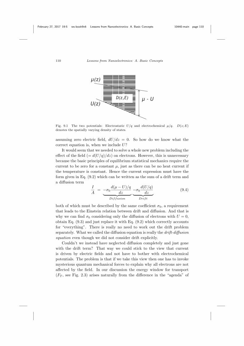
February 27, 2017 19:5 ws-book9x6 Lessons from Nanoelectronics: A. Basic Concepts 10440-main page 110
110 Lessons from Nanoelectronics: A. Basic Concepts
D(z,E)U(z)
µ(z)
µ - U
Fig. 9.1 The two potentials: Electrostatic U/q and electrochemical µ/q. D(z;E)denotes the spatially varying density of states.
assuming zero electric field, dU/dz = 0. So how do we know what the
correct equation is, when we include U?
It would seem that we needed to solve a whole new problem including the
effect of the field (= d(U/q)/dz) on electrons. However, this is unnecessary
because the basic principles of equilibrium statistical mechanics require the
current to be zero for a constant µ, just as there can be no heat current if
the temperature is constant. Hence the current expression must have the
form given in Eq. (9.2) which can be written as the sum of a drift term and
a diffusion termI
A= −σ0
d(µ− U)/q
dz︸ ︷︷ ︸Diffusion
−σ0d(U/q)
dz︸ ︷︷ ︸Drift
(9.4)
both of which must be described by the same coefficient σ0, a requirement
that leads to the Einstein relation between drift and diffusion. And that is
why we can find σ0 considering only the diffusion of electrons with U = 0,
obtain Eq. (9.3) and just replace it with Eq. (9.2) which correctly accounts
for “everything”. There is really no need to work out the drift problem
separately. What we called the diffusion equation is really the drift-diffusion
equation even though we did not consider drift explicitly.
Couldn’t we instead have neglected diffusion completely and just gone
with the drift term? That way we could stick to the view that current
is driven by electric fields and not have to bother with electrochemical
potentials. The problem is that if we take this view then one has to invoke
mysterious quantum mechanical forces to explain why all electrons are not
affected by the field. In our discussion the energy window for transport
(FT , see Fig. 2.3) arises naturally from the difference in the “agenda” of
February 27, 2017 19:5 ws-book9x6 Lessons from Nanoelectronics: A. Basic Concepts 10440-main page 111
Boltzmann Equation 111
the two contacts (see Eq. (2.10))
f1(E) − f2(E) =
(−∂f0
∂E
)(µ1 − µ2)
as discussed in Chapters 2 and 3.
The point is that regardless of which potential we choose to work with, it
finally affects transport through the occupation factor, f . In this chapter we
will justify our neglect of drift more explicitly by introducing the Boltzmann
Transport Equation (BTE) which is the standard starting point for all
discussions of the transport of particles. We too could have used it as the
starting point for but we did not do so because it is harder to digest with
its multiple independent variables, compared to the ordinary differential
equation in Chapter 8, which follows from relatively elementary arguments.
Even in this chapter we will not really do justice to the BTE. We will
introduce it briefly and use it to show that for low bias, the current indeed
depends only on dµ/dz and not on dU/dz, thus putting our discussion of
steady-state, low bias transport without electric fields on a firmer footing
and identifying possible issues with it.
Note the two qualifying phrases, namely “steady-state” and “low bias”.
We will show later in this chapter that for time varying transport, the ne-
glect of electric fields can lead to errors, but we will not discuss it further
in this book. However, even under steady-state conditions, electric fields
can play an important role in determining the full current-voltage charac-
teristics, once we go beyond low bias, as we saw in Chapter 7.
9.2 BTE from “Newton’s Laws”
In Chapter 8 we introduced electron distribution functions f± and electro-
chemical potentials µ± describing the drainbound and sourcebound currents
I±. Both the drainbound and sourcebound current, however, is composed
of electrons traveling at different angles having different z-momemtum pz,
even though they all have the same energy (we are still talking about an
elastic resistor) and hence the same total momentum. To include the effect
of the electric field we need “momentum-resolved” distribution functions
f±(z, pz, t).
The BTE describes the evolution of such “momentum-resolved” distri-
bution functions f(z, pz, t) that tell us the occupation of states with a given
momentum pz and velocity vz at a location z at time t:
∂f
∂t+ vz
∂f
∂z+ Fz
∂f
∂pz= Sopf (9.5)
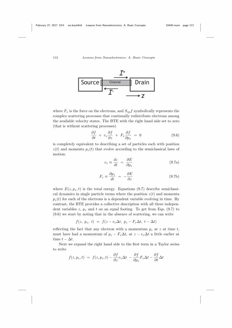
February 27, 2017 19:5 ws-book9x6 Lessons from Nanoelectronics: A. Basic Concepts 10440-main page 112
112 Lessons from Nanoelectronics: A. Basic Concepts
Source DrainI+
I-z
where Fz is the force on the electrons, and Sopf symbolically represents the
complex scattering processes that continually redistribute electrons among
the available velocity states. The BTE with the right hand side set to zero
(that is without scattering processes)
∂f
∂t+ vz
∂f
∂z+ Fz
∂f
∂pz= 0 (9.6)
is completely equivalent to describing a set of particles each with position
z(t) and momenta pz(t) that evolve according to the semiclassical laws of
motion:
vz ≡dz
dt=
∂E
∂pz(9.7a)
Fz ≡∂pzdt
= −∂E∂z
(9.7b)
where E(z, pz, t) is the total energy. Equations (9.7) describe semiclassi-
cal dynamics in single particle terms where the position z(t) and momenta
pz(t) for each of the electrons is a dependent variable evolving in time. By
contrast, the BTE provides a collective description with all three indepen-
dent variables z, pz and t on an equal footing. To get from Eqs. (9.7) to
(9.6) we start by noting that in the absence of scattering, we can write
f(z, pz, t) = f(z − vz∆t, pz − Fz∆t, t−∆t)
reflecting the fact that any electron with a momentum pz at z at time t,
must have had a momentum of pz − Fz∆t, at z − vz∆t a little earlier at
time t−∆t.
Next we expand the right hand side to the first term in a Taylor series
to write
f(z, pz, t) = f(z, pz, t)−∂f
∂zvz∆t −
∂f
∂pzFz∆t−
∂f
∂t∆t
February 27, 2017 19:5 ws-book9x6 Lessons from Nanoelectronics: A. Basic Concepts 10440-main page 113
Boltzmann Equation 113
Eq. (9.6) follows readily on canceling out the common terms. The left
hand side of the BTE thus represents an alternative way of expressing the
laws of motion. What makes it different from mere mechanics, however,
is the stochastic scattering term on the right which makes the distribution
function f approach the equilibrium Fermi function when external driving
terms are absent. This last point of course is not meant to be obvious. It
requires an extended discussion of the scattering operator Sop that we talk
a little more about in Chapter 15 when we discuss the second law. For our
purpose it suffices to note that a common approximation for the scattering
term is the relaxation time approximation (RTA)
Sopf ∼= − f − fτ
(9.8)
which assumes that the effect of the scattering processes is proportional to
the degree to which a given distribution f differs from the local equilibrium
distribution f .
One comment about why we call this approach semiclassical. The BTE
is classical in the sense that it is based on a particle view of electrons. But
it is not fully classical, since it typically includes quantum input both in the
scattering operator Sop and in the form of the energy-momentum relation.
For example, graphene is often described by a linear energy-momentum
relation
E = ν0p
a result that is usually justified in terms of the bandstructure of the
graphene lattice requiring quantum mechanics that came after Boltzmann’s
time. This is also why we put Newton’s laws within quotes in the section
title. But once we accept this extension, many transport properties of
graphene can be understood in classical particulate terms using the BTE
that Boltzmann taught us to use.
9.3 Diffusion Equation from BTE
We start by combining the RTA (Eq. (9.8)) with the full BTE (Eq. (9.5))
to obtain for steady-state (∂/∂t = 0),
vz∂f
∂z+ Fz
∂f
∂pz= − f − f
τ. (9.9)
In the presence of an electric field we can write the total energy as
E(z, pz) = ε(pz) + U(z) (9.10)

February 27, 2017 19:5 ws-book9x6 Lessons from Nanoelectronics: A. Basic Concepts 10440-main page 114
114 Lessons from Nanoelectronics: A. Basic Concepts
μ0
pz pz
z=z1 z=z2
U(z1)
E = (pz )+U(z)
U(z2)
Fig. 9.2 The energy momentum relation with U = 0 is shifted locally by U(z). At
equilibrium the electrochemical potential µ0 is spatially constant.
where ε(pz) denotes the energy-momentum relation with U = 0 and this
gets shifted locally by U(z) as sketched in Fig. 9.2.
The first point to note is that the equilibrium distribution with a con-
stant electrochemical potential µ0
f0(z, pz) =1
exp
(E(z, pz)− µ0
kT
)+ 1
(9.11)
satisfies the BTE in Eq. (9.9). The right hand side of Eq. (9.9) is zero
simply because f = f0, but it takes a little differential calculus to see that
the left hand side is zero too. Defining
X0 ≡ E(z, pz) − µ0 = ε(pz) + U(z)− µ0 (9.12)
we have
vz∂f0
∂z+ Fz
∂f0
∂pz=
(∂f0
∂X0
) (vz∂X0
∂z+ Fz
∂X0
∂pz
)
=
(∂f0
∂X0
) (vz∂E
∂z+ Fz
∂E
∂pz
)= 0
making use of Eqs. (9.7).
Out of equilibrium, we assume two separate distribution functions
f±(z, pz) as in Eqs. (8.17a) and (8.17b) for the right-moving (vz > 0)
and the left-moving (vz < 0) electrons with separate spatially varying elec-
trochemical potentials µ±(z):
f±(z, pz) =1
exp
(E(z, pz)− µ±(z)
kT
)+ 1
(9.13)

February 27, 2017 19:5 ws-book9x6 Lessons from Nanoelectronics: A. Basic Concepts 10440-main page 115
Boltzmann Equation 115
μ(z)
pz pz
z=z1 z=z2
U(z1)
E = (pz )+U(z)
U(z2)
Fig. 9.3 Same as Fig. 9.2, but the electrochemical potential µ(z) varies spatially
reflecting a non-equilibrium state.
Using Eq. (9.13), the left hand side of BTE (see Eq. (9.9)) reduces to(∂f
∂X
) (vz∂X
∂z+ Fz
∂X
∂pz
)=
(∂f
∂X
) (−vz
∂µ±
∂z
)(9.14)
where
X± ≡ E(z, pz)− µ±(z).
We now assume small deviations in µ±(z) from the local equilibrium
value so that we can write the left hand side as(∂f
∂X
)X=X
(−vz
∂µ±
∂z
)and use our standard Taylor series expansion (see Eq. (2.11)) to write the
right hand side of BTE as
− f± − fτ
≈(∂f
∂X
)X=X
µ± − µτ
.
Combining the two sides
vz∂µ±
∂z= −µ
± − µτ
. (9.15)
This gives us two separate equations for the two electrochemical poten-
tials µ+ and µ− for the right-moving (vz > 0) and left-moving (vz < 0)
electrons∂µ+
∂z= −µ
+ − µ|vz|τ
,∂µ−
∂z= −µ
− − µ−|vz|τ
.
Assuming µ = (µ+ + µ−)/2, we obtain∂µ+
∂z= −µ
+ − µ−
λ=
∂µ−
∂z(9.16)
with λ = 2|vz|τ . Combining with Eq. (8.10) for the current, we obtain the
result (Eq. (8.13)) stated without proof in Chapter 8. Note that we have
included electric fields explicitly and shown that their effect cancels out.
February 27, 2017 19:5 ws-book9x6 Lessons from Nanoelectronics: A. Basic Concepts 10440-main page 116
116 Lessons from Nanoelectronics: A. Basic Concepts
9.3.1 Equilibrium fields can matter
We believe, however, that there is an important subtlety worth pointing
out. Although the externally applied electric field does not affect the low
bias conductance, any inbuilt fields that exist within the conductor under
equilibrium conditions can affect its low bias conductance. Let me explain.
Note that in our treatment above we assumed that under non-equilibrium
conditions, the electrochemical potential is a function of z (Eq. (9.13))
and the resulting linearized equation (Eq. (9.16)) does not involve the field
Fz = dU/dz. However, the field term would not have dropped out so nicely
if we were to assume that the electrochemical potential is not just a function
of z, but of both z and pz. Instead of Eq. (9.15) we would then obtain
vz∂µ
∂z+ Fz
∂µ
∂pz= −µ− µ
τ. (9.17)
However, the additional term involving the field Fz does not play a role
in determining linear conductivity because it is ∼ V 2, V being the applied
voltage. At equilibrium with V = 0, µ = µ, so that both derivatives
appearing on the left are zero. Under bias, in principle, both are non-zero.
But the point is that while vz is a constant, the applied field Fz is also ∼ V .
So while the first term on the left is ∼ V , the second term is ∼ V 2.
But this argument would not hold if Fz were not the applied field, but
internal inbuilt fields independent of V that are present even at equilib-
rium. Equilibrium requires a constant µ and NOT a constant U . The
equilibrium condition depicted in Fig. 9.2 is quite common in real con-
ductors, with varying U(z) corresponding to non-zero fields Fz. Indeed
this picture could also represent an interface between dissimilar materials
(called “heterostructures”) where the discontinuity in band edges is often
modeled with effective fields.
The point is that such equilibrium fields can affect the low bias conduc-
tance. For an ideal homogeneous conductor we do not have such fields. But
even then we need to make two contacts in order to measure the resistance.
Each such contact represents a heterostructure qualitatively similar to that
shown in Fig. 9.2 with inbuilt effective (if not real) fields. In Chapter 11 we
will discuss the Hall effect where we have to keep the Fz term in Eq. (9.17)
in order to account for the presence of an external magnetic field.
9.4 The Two Potentials
In this book we will generally focus on steady-state transport involving the
injection of electrons from a source and their collection by a drain (Fig. 9.4).

February 27, 2017 19:5 ws-book9x6 Lessons from Nanoelectronics: A. Basic Concepts 10440-main page 117
Boltzmann Equation 117
We have seen that the low bias conductance can be understood in terms of
the electrochemical potential µ, without worrying about the electrostatic
potential U . However, we would like to briefly consider ac transport through
a nanowire far from any contacts where we have a local voltage V (z, t) and
current I(z, t) (Fig. 9.5), because this provides a contrasting example where
it is important to pay attention to the difference between the two potentials
even for low bias, in order to obtain the correct inductance and capacitance.
Source Drain
VI
zFig. 9.4 So far we have talked of steady-state transport involving the injection of elec-trons by a source and their collection by a drain contact.
~
IV
z
Fig. 9.5 AC or time varying transport along a nanowire can be described in terms of a
voltage V (z, t) and a current I(z, t).
For this problem too we start from the BTE with the RTA approxima-
tion as in the last section, but we do not set ∂/∂t = 0. Instead we start
from
∂f
∂t+ vz
∂f
∂z+ Fz
∂f
∂pz= −f − f
τ

February 27, 2017 19:5 ws-book9x6 Lessons from Nanoelectronics: A. Basic Concepts 10440-main page 118
118 Lessons from Nanoelectronics: A. Basic Concepts
and linearize it assuming a distribution of the form (compare Eq. (9.13))
f(z, pz, t) =1
exp
(E(z, pz, t)− µ(z, t)
kT
)+ 1
. (9.18)
Compared to the steady-state problem (Eq. (9.15)) we now have two extra
terms involving the time derivatives of E and µ:
∂µ
∂t+ vz
∂µ
∂z− ∂E
∂t= −µ− µ
τ. (9.19)
As we did in the last Section with Eq. (9.15), we can separate Eq. (9.19)
into two equations for µ+ and µ−, whose sum and difference are identified
with voltage and current to obtain a set of equations
∂(µ/q)
∂z= −(LK + LM )
∂I
∂t− I
σA(9.20a)
∂(µ/q)
∂t= −
(1
CQ+
1
CE
)∂I
∂z(9.20b)
that look just like the transmission line equations with a distributed series
inductance and resistance and a shunt capacitance.
The algebra getting from Eq. (9.19) to Eqs. (9.20) is a little long-winded
and since time-varying transport is only incidental to our main message
we have relegated the details to Appendix E. Those who are really in-
terested can look at the original paper on which this discussion is based
(Salahuddin et al., 2005). But note the two inductors and the two capaci-
tors in series. The kinetic inductance LK and the quantum capacitance CQper unit length, arise from transport-related effects
LK =h
q2
1
〈2Mvz〉(9.21a)
CQ =q2
h
⟨2M
vz
⟩(9.21b)
while the LM and the CE are just the normal magnetic inductance and the
electrostatic capacitance from the equations of magnetostatics and electro-
statics. The point I wish to make is that the fields enter the expression for
the energy E(z, pz, t) and if we ignore the fields we would miss the ∂E/∂t
term in Eq. (9.19) to obtain
∂µ
∂t+ vz
∂µ
∂z= −µ− µ
τ(9.22)
February 27, 2017 19:5 ws-book9x6 Lessons from Nanoelectronics: A. Basic Concepts 10440-main page 119
Boltzmann Equation 119
and after working through the algebra obtain instead of Eqs. (9.20)
∂(µ/q)
∂z= −LK
∂I
∂t− I
σA(9.23a)
∂(µ/q)
∂t= − 1
CQ
∂I
∂z. (9.23b)
Do these equations approximately capture the physics? Not unless we are
considering wires with very small cross-sections so that M is a small number
making LK LM and CQ CE . We could recover the correct answer
from Eqs. (9.23) by replacing the µ with µ− U and then using the laws of
electromagnetics to replace
∂U
∂twith
1
CE
∂I
∂zand
∂U
∂zwith LM
∂I
∂t.
But these replacements may not be obvious and it is more straightfor-
ward to go from Eq. (9.19) to (9.20) as spelt out in Appendix E. Note that
if we specialize to steady-state (∂/∂t = 0), both Eqs. (9.19) and (9.22) give
us back our old diffusion equation (Eq. (8.2)). As we argued earlier, for
low bias steady-state transport, the applied electric field can be treated as
incidental.

February 27, 2017 19:5 ws-book9x6 Lessons from Nanoelectronics: A. Basic Concepts 10440-main page 120

February 27, 2017 19:5 ws-book9x6 Lessons from Nanoelectronics: A. Basic Concepts 10440-main page 121
Chapter 10
Quasi-Fermi Levels
10.1 Introduction
Electrochemical potentials have played an important role in our discussion,
starting from Chapter 2 where I stressed that electron flow is driven by the
difference in the electrochemical potentials µ1 and µ2 in the two contacts.
However, talking about electrochemical potentials inside the channel, as we
did later in Chapter 8 when discussing the diffusion equation, often raises
eyebrows. This is because an electrochemical potential of µ implies that
the occupation of all available states are described by the corresponding
Fermi function (Eq. (2.2))
f(E) =1
1 + exp
(E − µkT
) .This is approximately true of large contacts which always remain close
to equilibrium, but not necessarily true of small conductors even for small
applied voltages. As we saw in Chapter 8, it was important to introduce two
separate electrochemical potentials µ+ and µ− in order to understand the
interface resistance that is the key feature of the new Ohm’s law (Eq. (4.5)).
Non-equilibrium electrochemical potentials of this type can be very use-
ful in understanding current flow and is widely used by device engineers. It
is common to use two different potentials (often called quasi-Fermi levels)
for conduction and valence bands and in Chapter 12 we will talk about other
examples of quasi-Fermi levels and argue that controlling such potentials
with creatively designed “smart” contacts could lead to unique devices.
In spite of the obvious utility of the concept, many experts are uneasy
about invoking non-equilibrium electrochemical potentials inside nanoscale
devices which they view as ill-defined concepts that cannot be measured.
121
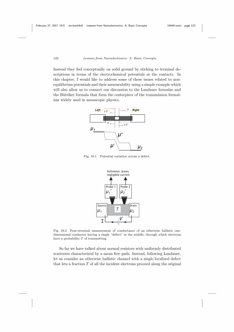
February 27, 2017 19:5 ws-book9x6 Lessons from Nanoelectronics: A. Basic Concepts 10440-main page 122
122 Lessons from Nanoelectronics: A. Basic Concepts
Instead they feel conceptually on solid ground by sticking to terminal de-
scriptions in terms of the electrochemical potentials at the contacts. In
this chapter, I would like to address some of these issues related to non-
equilibrium potentials and their measurability using a simple example which
will also allow us to connect our discussion to the Landauer formulas and
the Buttiker formula that form the centerpiece of the transmission formal-
ism widely used in mesoscopic physics.
T1-T
T1-T
Left Right
µ1
µ2
µ+
µ-
Fig. 10.1 Potential variation across a defect.
Source
µ1
Drain
µ2
Probe 1
µ1*
Probe 2
µ2*
V
Voltmeter, drawsnegligible current
I
Fig. 10.2 Four-terminal measurement of conductance of an otherwise ballistic one-dimensional conductor having a single “defect” in the middle, through which electronshave a probability T of transmitting.
So far we have talked about normal resistors with uniformly distributed
scatterers characterized by a mean free path. Instead, following Landauer,
let us consider an otherwise ballistic channel with a single localized defect
that lets a fraction T of all the incident electrons proceed along the original
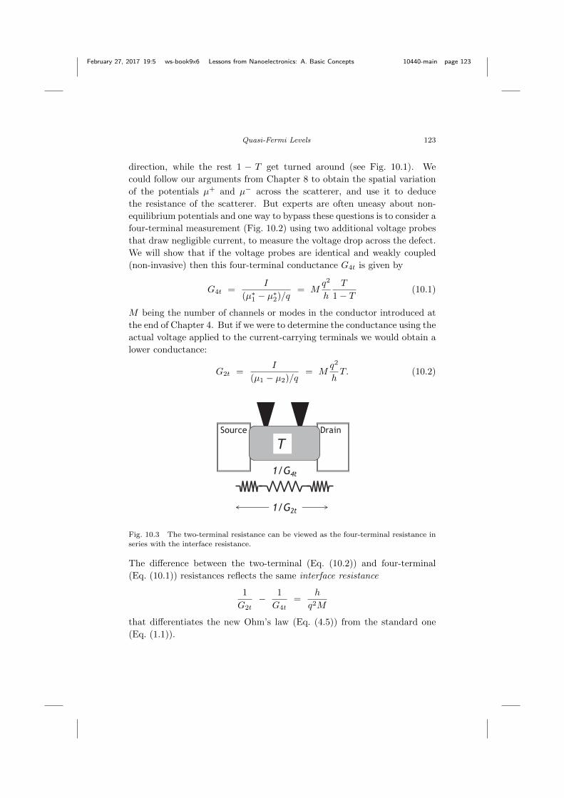
February 27, 2017 19:5 ws-book9x6 Lessons from Nanoelectronics: A. Basic Concepts 10440-main page 123
Quasi-Fermi Levels 123
direction, while the rest 1 − T get turned around (see Fig. 10.1). We
could follow our arguments from Chapter 8 to obtain the spatial variation
of the potentials µ+ and µ− across the scatterer, and use it to deduce
the resistance of the scatterer. But experts are often uneasy about non-
equilibrium potentials and one way to bypass these questions is to consider a
four-terminal measurement (Fig. 10.2) using two additional voltage probes
that draw negligible current, to measure the voltage drop across the defect.
We will show that if the voltage probes are identical and weakly coupled
(non-invasive) then this four-terminal conductance G4t is given by
G4t =I
(µ∗1 − µ∗2)/q= M
q2
h
T
1− T(10.1)
M being the number of channels or modes in the conductor introduced at
the end of Chapter 4. But if we were to determine the conductance using the
actual voltage applied to the current-carrying terminals we would obtain a
lower conductance:
G2t =I
(µ1 − µ2)/q= M
q2
hT. (10.2)
Source Drain
1/G4t
1/G2t
Fig. 10.3 The two-terminal resistance can be viewed as the four-terminal resistance inseries with the interface resistance.
The difference between the two-terminal (Eq. (10.2)) and four-terminal
(Eq. (10.1)) resistances reflects the same interface resistance
1
G2t− 1
G4t=
h
q2M
that differentiates the new Ohm’s law (Eq. (4.5)) from the standard one
(Eq. (1.1)).

February 27, 2017 19:5 ws-book9x6 Lessons from Nanoelectronics: A. Basic Concepts 10440-main page 124
124 Lessons from Nanoelectronics: A. Basic Concepts
Although the interface resistance was recognized for metallic resistors
in the late 1960s and is known as the Sharvin resistance, its ubiquitous
role is not widely appreciated even today. In the early 1980s there was
considerable confusion and discussion about the difference between the two
conductance formulas in Eqs. (10.1) and (10.2) and Imry is credited with
identifying the difference as a quantized Sharvin resistance related to the
interfaces. With the rise of mesoscopic physics, Eq. (10.2) has come to be
widely used and known as the Landauer formula while Landauer’s original
formula (Eq. (10.1)) is relatively forgotten, and not many recognize the
difference.
The reader may wonder why the four-terminal Landauer formula came
to be “forgotten”. After all resistance measurements are commonly made in
the four terminal configuration in order to exclude any contact resistance.
Don’t such measurements require Eq. (10.1) for their interpretation? Sort
of, but not exactly. Let me explain.
One problem in the early days of mesoscopic physics was that the volt-
age probes were strongly coupled to the main conductor and behaved like
“additional defects” whose effect could not simply be ignored. In order to
interpret real experiments using four-terminal configurations, Buttiker (see
Buttiker 1988) found an elegant solution by writing the current Im at ter-
minal m of a multi-terminal conductor in terms of the terminal potentials
µn:
Im =1
q
∑m
Gm,n (µm − µn) (10.3)
where Gm,n is the conductance determined by the transmission Tm,n be-
tween terminals m and n. With just two terminals, Buttiker’s formula
reduces to
I1 = (1/q) G12 (µ1 − µ2) = −I2which is the same as the two-terminal Landauer formula (Eq. (10.2)) if we
identify G12 as (q2/h)M . But the power of Eq. (10.3) lies in its ability to
provide a quantitative basis for the analysis of multi-terminal structures
like the one in Fig. 10.2.
Knowing Gm,n, if we knew all the potentials µm, we could use Eq. (10.3)
to calculate the currents Im at all the terminals. Of course for the voltage
probes 1∗ and 2∗ we do not know the voltages they will float to and so we
do not know µ∗1 or µ∗2, to start with. But we do know the currents I∗1 and
I∗2 , each of which must be zero, since the high impedance voltmeter draws
negligible current.
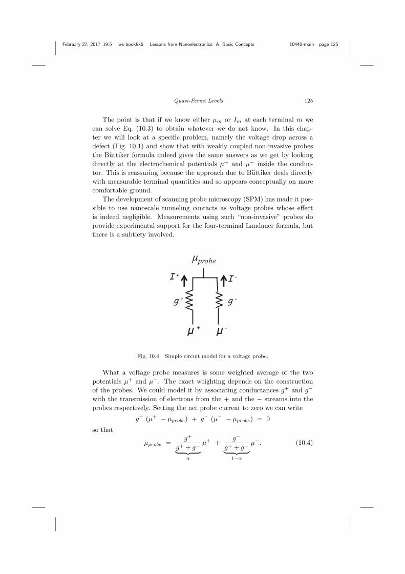
February 27, 2017 19:5 ws-book9x6 Lessons from Nanoelectronics: A. Basic Concepts 10440-main page 125
Quasi-Fermi Levels 125
The point is that if we know either µm or Im at each terminal m we
can solve Eq. (10.3) to obtain whatever we do not know. In this chap-
ter we will look at a specific problem, namely the voltage drop across a
defect (Fig. 10.1) and show that with weakly coupled non-invasive probes
the Buttiker formula indeed gives the same answers as we get by looking
directly at the electrochemical potentials µ+ and µ− inside the conduc-
tor. This is reassuring because the approach due to Buttiker deals directly
with measurable terminal quantities and so appears conceptually on more
comfortable ground.
The development of scanning probe microscopy (SPM) has made it pos-
sible to use nanoscale tunneling contacts as voltage probes whose effect
is indeed negligible. Measurements using such “non-invasive” probes do
provide experimental support for the four-terminal Landauer formula, but
there is a subtlety involved.
I +
µprobeI -
µ + µ -
g -g +
Fig. 10.4 Simple circuit model for a voltage probe.
What a voltage probe measures is some weighted average of the two
potentials µ+ and µ−. The exact weighting depends on the construction
of the probes. We could model it by associating conductances g+ and g−
with the transmission of electrons from the + and the − streams into the
probes respectively. Setting the net probe current to zero we can write
g+ (µ+ − µprobe) + g− (µ− − µprobe) = 0
so that
µprobe =g+
g+ + g−︸ ︷︷ ︸α
µ+ +g−
g+ + g−︸ ︷︷ ︸1−α
µ−. (10.4)

February 27, 2017 19:5 ws-book9x6 Lessons from Nanoelectronics: A. Basic Concepts 10440-main page 126
126 Lessons from Nanoelectronics: A. Basic Concepts
For atomic scale probes that are much smaller than an electron wave-
length we expect the two conductances to be similar so that the weighting
factor α ∼ 50%, so that the probe measures the average potential
µprobe = (µ+ + µ−)/2.
For larger probes, however, it is possible for a voltage probe to have a
pronounced bias for one stream or the other leading to a weighting factor
α different from 50%. If this weighting happens to be different for the
two probes 1∗ and 2∗, it could change the measured resistance from that
predicted by Eq. (10.1). Indeed, experimental measurements have even
shown negative resistance, something that cannot be understood in terms
of Eq. (10.1).
However, some of this is due to quantum interference effects that make
the simple semiclassical description in terms of µ± inadequate as we will see
in Part B. However, one could use a more sophisticated quantum version
of Eq. (10.4) or use the Buttiker formula, with the conductances Gm,ncalculated from an appropriate quantum transport model.
The bottom line is that if we know the correct internal state of the
conductor in terms of a set of non-equilibrium electrochemical potentials,
we can predict what a specific non-invasive voltage probe will measure and
the result should match what the Buttiker formula predicts. The reverse,
however, is not true. Knowing what a specific probe will measure, we
cannot deduce the internal state of the conductor.
With that rather long “introduction” let us now look at the two
Landauer formulas (Eqs. (10.1) and (10.2)) and the Buttiker formula
(Eq. (10.3)) in a little more detail.
10.2 The Landauer Formulas (Eqs. (10.1) and (10.2))
Related video lecture available at course website, Unit 3: L3.5.
Getting back to the problem of finding the potential variation across a
defect in an otherwise ballistic conductor (Fig. 10.1), we start by relating
the outgoing currents to the incoming currents as follows
I+(Right) = TI+(Left) + (1− T )I−(Right)
I−(Left) = (1− T )I+(Left) + TI−(Right).
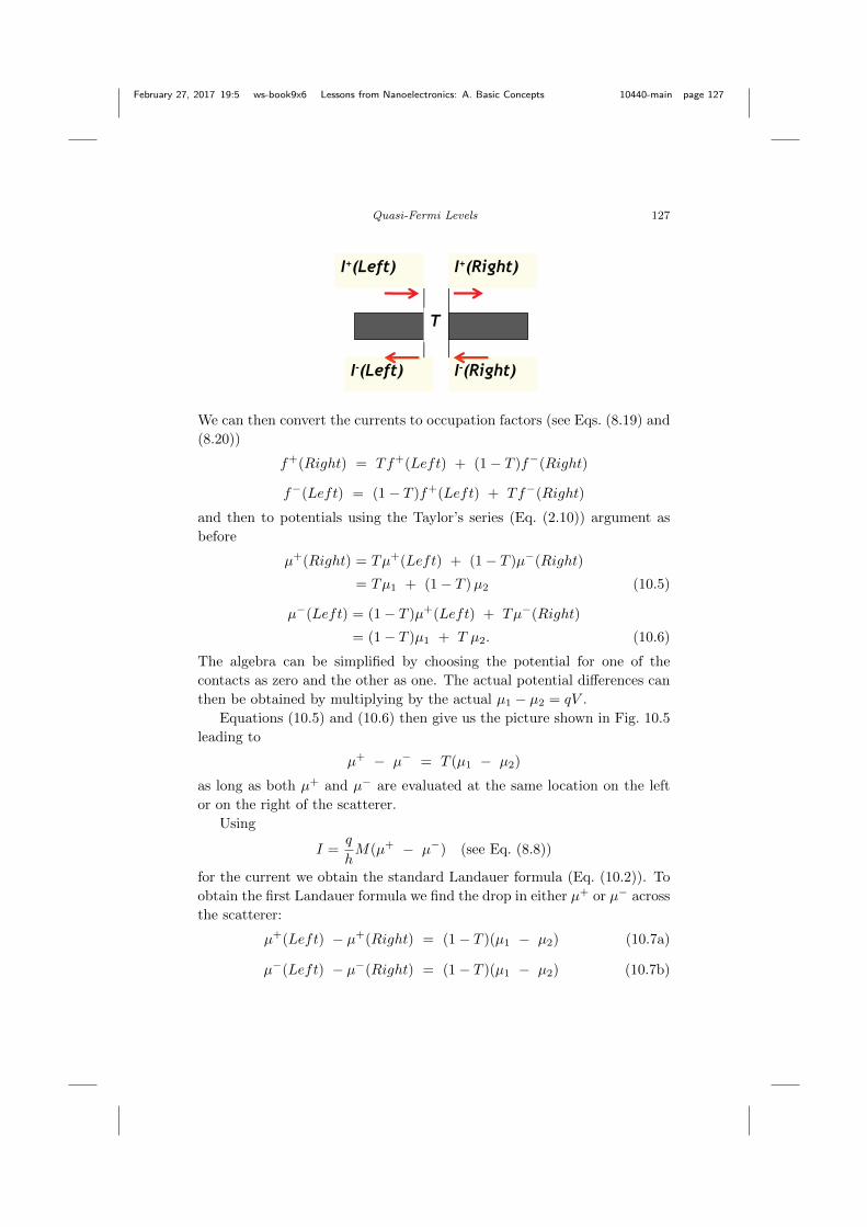
February 27, 2017 19:5 ws-book9x6 Lessons from Nanoelectronics: A. Basic Concepts 10440-main page 127
Quasi-Fermi Levels 127
I+(Left) I+(Right)
T
I-(Left) I-(Right)
We can then convert the currents to occupation factors (see Eqs. (8.19) and
(8.20))
f+(Right) = Tf+(Left) + (1− T )f−(Right)
f−(Left) = (1− T )f+(Left) + Tf−(Right)
and then to potentials using the Taylor’s series (Eq. (2.10)) argument as
before
µ+(Right) = Tµ+(Left) + (1− T )µ−(Right)
= Tµ1 + (1− T )µ2 (10.5)
µ−(Left) = (1− T )µ+(Left) + Tµ−(Right)
= (1− T )µ1 + T µ2. (10.6)
The algebra can be simplified by choosing the potential for one of the
contacts as zero and the other as one. The actual potential differences can
then be obtained by multiplying by the actual µ1 − µ2 = qV .
Equations (10.5) and (10.6) then give us the picture shown in Fig. 10.5
leading to
µ+ − µ− = T (µ1 − µ2)
as long as both µ+ and µ− are evaluated at the same location on the left
or on the right of the scatterer.
Using
I =q
hM(µ+ − µ−) (see Eq. (8.8))
for the current we obtain the standard Landauer formula (Eq. (10.2)). To
obtain the first Landauer formula we find the drop in either µ+ or µ− across
the scatterer:
µ+(Left) − µ+(Right) = (1− T )(µ1 − µ2) (10.7a)
µ−(Left) − µ−(Right) = (1− T )(µ1 − µ2) (10.7b)
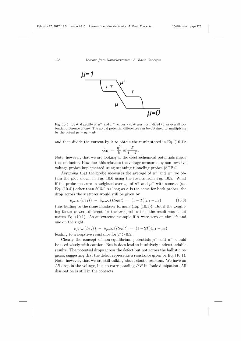
February 27, 2017 19:5 ws-book9x6 Lessons from Nanoelectronics: A. Basic Concepts 10440-main page 128
128 Lessons from Nanoelectronics: A. Basic Concepts
µ=1
µ=0
T1- T
µ+
µ-
Fig. 10.5 Spatial profile of µ+ and µ− across a scatterer normalized to an overall po-
tential difference of one. The actual potential differences can be obtained by multiplyingby the actual µ1 − µ2 = qV .
and then divide the current by it to obtain the result stated in Eq. (10.1):
G4t =q2
hM
T
1− T.
Note, however, that we are looking at the electrochemical potentials inside
the conductor. How does this relate to the voltage measured by non-invasive
voltage probes implemented using scanning tunneling probes (STP)?
Assuming that the probe measures the average of µ+ and µ− we ob-
tain the plot shown in Fig. 10.6 using the results from Fig. 10.5. What
if the probe measures a weighted average of µ+ and µ− with some α (see
Eq. (10.4)) other than 50%? As long as α is the same for both probes, the
drop across the scatterer would still be given by
µprobe(Left) − µprobe(Right) = (1− T )(µ1 − µ2) (10.8)
thus leading to the same Landauer formula (Eq. (10.1)). But if the weight-
ing factor α were different for the two probes then the result would not
match Eq. (10.1). As an extreme example if α were zero on the left and
one on the right,
µprobe(Left) − µprobe(Right) = (1− 2T )(µ1 − µ2)
leading to a negative resistance for T > 0.5.
Clearly the concept of non-equilibrium potentials µ+ and µ− should
be used wisely with caution. But it does lead to intuitively understandable
results. The potential drops across the defect but not across the ballistic re-
gions, suggesting that the defect represents a resistance given by Eq. (10.1).
Note, however, that we are still talking about elastic resistors. We have an
IR drop in the voltage, but no corresponding I2R in Joule dissipation. All
dissipation is still in the contacts.
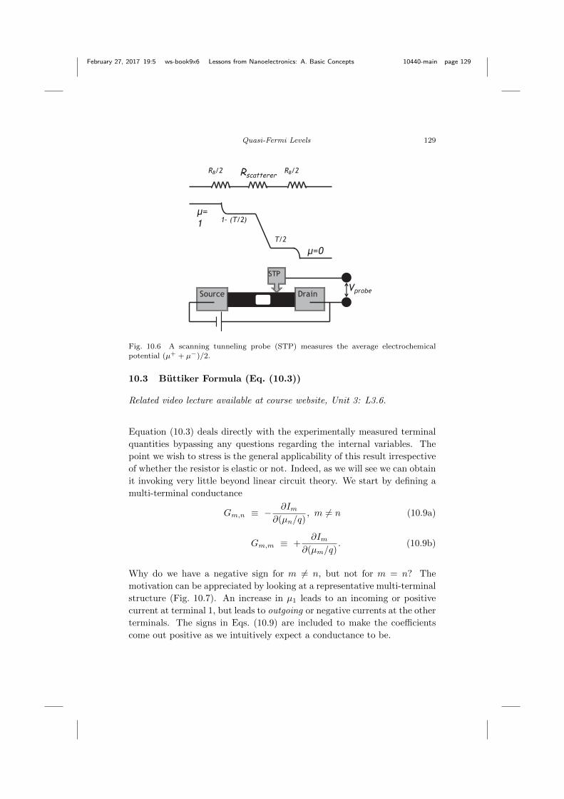
February 27, 2017 19:5 ws-book9x6 Lessons from Nanoelectronics: A. Basic Concepts 10440-main page 129
Quasi-Fermi Levels 129
Source DrainVprobe
STP
µ=1
µ=0T/2
1- (T/2)
RB/2 Rscatterer RB/2
Fig. 10.6 A scanning tunneling probe (STP) measures the average electrochemical
potential (µ+ + µ−)/2.
10.3 Buttiker Formula (Eq. (10.3))
Related video lecture available at course website, Unit 3: L3.6.
Equation (10.3) deals directly with the experimentally measured terminal
quantities bypassing any questions regarding the internal variables. The
point we wish to stress is the general applicability of this result irrespective
of whether the resistor is elastic or not. Indeed, as we will see we can obtain
it invoking very little beyond linear circuit theory. We start by defining a
multi-terminal conductance
Gm,n ≡ −∂Im
∂(µn/q), m 6= n (10.9a)
Gm,m ≡ +∂Im
∂(µm/q). (10.9b)
Why do we have a negative sign for m 6= n, but not for m = n? The
motivation can be appreciated by looking at a representative multi-terminal
structure (Fig. 10.7). An increase in µ1 leads to an incoming or positive
current at terminal 1, but leads to outgoing or negative currents at the other
terminals. The signs in Eqs. (10.9) are included to make the coefficients
come out positive as we intuitively expect a conductance to be.
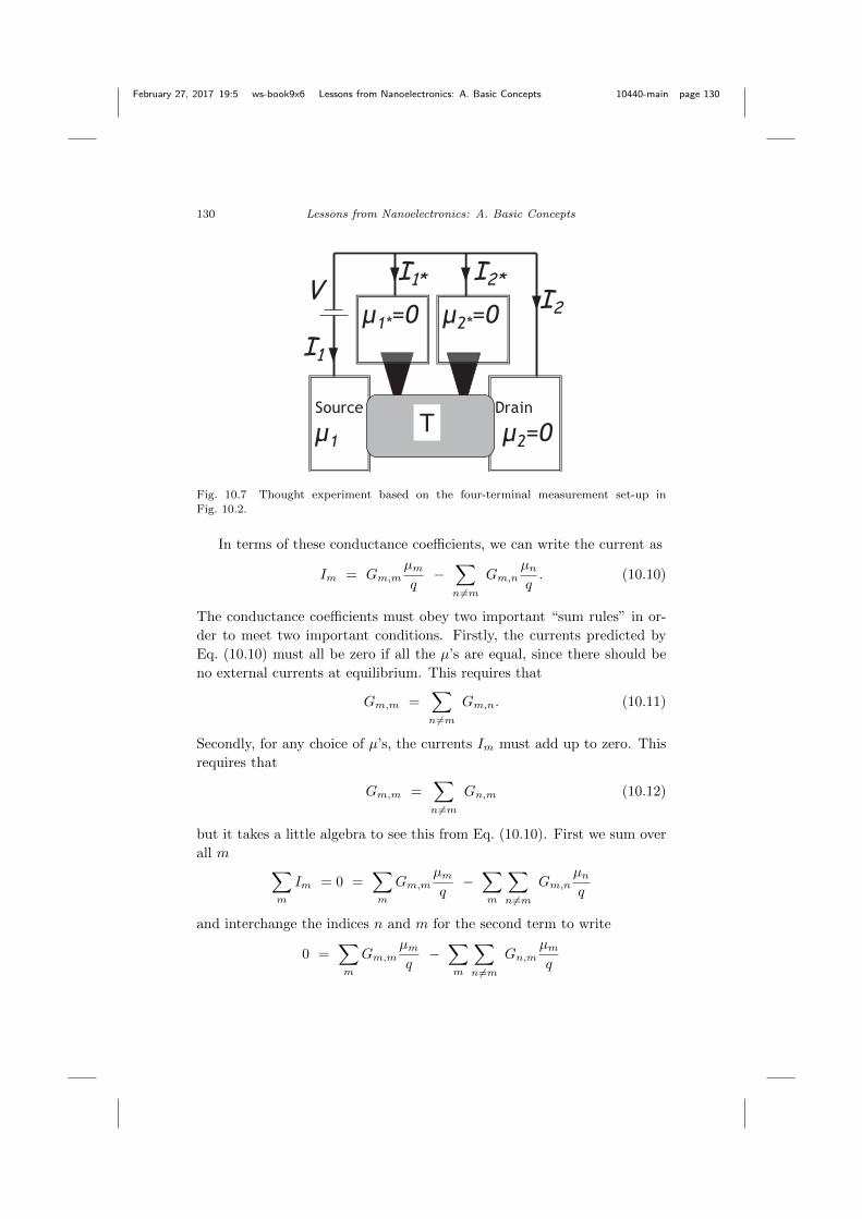
February 27, 2017 19:5 ws-book9x6 Lessons from Nanoelectronics: A. Basic Concepts 10440-main page 130
130 Lessons from Nanoelectronics: A. Basic Concepts
Source
µ1
Drain
µ2=0
V
I1
I1*I2
I2*µ1*=0 µ2*=0
Fig. 10.7 Thought experiment based on the four-terminal measurement set-up in
Fig. 10.2.
In terms of these conductance coefficients, we can write the current as
Im = Gm,mµmq−∑n 6=m
Gm,nµnq. (10.10)
The conductance coefficients must obey two important “sum rules” in or-
der to meet two important conditions. Firstly, the currents predicted by
Eq. (10.10) must all be zero if all the µ’s are equal, since there should be
no external currents at equilibrium. This requires that
Gm,m =∑n 6=m
Gm,n. (10.11)
Secondly, for any choice of µ’s, the currents Im must add up to zero. This
requires that
Gm,m =∑n 6=m
Gn,m (10.12)
but it takes a little algebra to see this from Eq. (10.10). First we sum over
all m ∑m
Im = 0 =∑m
Gm,mµmq−∑m
∑n 6=m
Gm,nµnq
and interchange the indices n and m for the second term to write
0 =∑m
Gm,mµmq−∑m
∑n6=m
Gn,mµmq

February 27, 2017 19:5 ws-book9x6 Lessons from Nanoelectronics: A. Basic Concepts 10440-main page 131
Quasi-Fermi Levels 131
which can be true for all choices of µm only if Eq. (10.12) is satisfied. We
can combine Eqs. (10.11) and (10.12) to obtain the “sum rule” succinctly:
Gm,m =∑n 6=m
Gm,n =∑n 6=m
Gn,m. (10.13)
Making use of the sum rule (Eq. (10.13)) we can re-write the first term in
Eq. (10.10) to obtain Eq. (10.3):
Im =
(1
q
)∑n
Gm,n(µm − µn) (same as Eq. (10.3)).
Note that it is not necessary to restrict the summation to n 6= m, since
the term with n = m is zero anyway. An alternate form that is sometimes
useful is to write
Im =∑n
gm,nµnq
(10.14)
where the response coefficients defined as
gm,n ≡ −Gm,n, m 6= n (10.15)
gm,m ≡ Gm,m. (10.16)
The sum rule in Eq. (10.13) can be rewritten in term of this new response
coefficient: ∑n
gm,n =∑n
gn,m = 0. (10.17)
10.3.1 Application
In Section 10.2 we analyzed the potential profile across a single scatterer
with transmission probability T . Based on this discussion we would expect
that two non-invasive probes inserted before and after the scatterer should
float to potentials 1 − (T/2) and T/2 as indicated in Fig. 10.8. But will
Buttiker’s approach get us the same result?
We start from Eq. (10.14) noting that we have four currents and four
potentials, labeled 1, 2, 1∗ and 2∗:I1I2I∗1I∗2
=Mq
h
[A B
C D
]µ1
µ2
µ∗1µ∗2
(10.18)
where A, B, C and D are each (2×2) matrices.
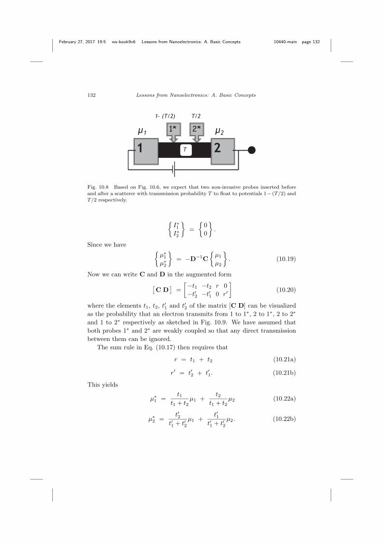
February 27, 2017 19:5 ws-book9x6 Lessons from Nanoelectronics: A. Basic Concepts 10440-main page 132
132 Lessons from Nanoelectronics: A. Basic Concepts
µ1 µ2
1 2T
2*T/21- (T/2)
1*
Fig. 10.8 Based on Fig. 10.6, we expect that two non-invasive probes inserted before
and after a scatterer with transmission probability T to float to potentials 1− (T/2) and
T/2 respectively.
I∗1I∗2
=
0
0
.
Since we have µ∗1µ∗2
= −D−1C
µ1
µ2
. (10.19)
Now we can write C and D in the augmented form[C D
]=
[−t1 −t2 r 0
−t′2 −t′1 0 r′
](10.20)
where the elements t1, t2, t′1 and t′2 of the matrix [C D] can be visualized
as the probability that an electron transmits from 1 to 1∗, 2 to 1∗, 2 to 2∗
and 1 to 2∗ respectively as sketched in Fig. 10.9. We have assumed that
both probes 1∗ and 2∗ are weakly coupled so that any direct transmission
between them can be ignored.
The sum rule in Eq. (10.17) then requires that
r = t1 + t2 (10.21a)
r′ = t′2 + t′1. (10.21b)
This yields
µ∗1 =t1
t1 + t2µ1 +
t2t1 + t2
µ2 (10.22a)
µ∗2 =t′2
t′1 + t′2µ1 +
t′1t′1 + t′2
µ2. (10.22b)
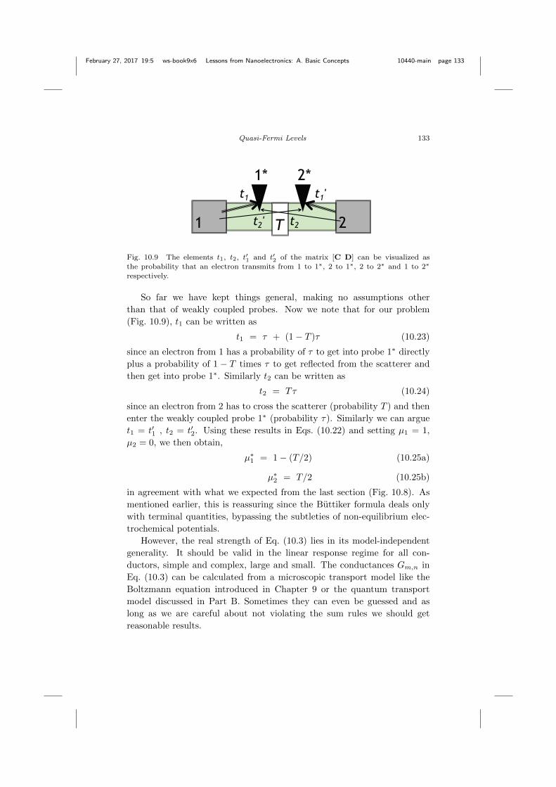
February 27, 2017 19:5 ws-book9x6 Lessons from Nanoelectronics: A. Basic Concepts 10440-main page 133
Quasi-Fermi Levels 133
1
1* 2*t1
t2' t2
t1'
2T
Fig. 10.9 The elements t1, t2, t′1 and t′2 of the matrix [C D] can be visualized as
the probability that an electron transmits from 1 to 1∗, 2 to 1∗, 2 to 2∗ and 1 to 2∗
respectively.
So far we have kept things general, making no assumptions other
than that of weakly coupled probes. Now we note that for our problem
(Fig. 10.9), t1 can be written as
t1 = τ + (1− T )τ (10.23)
since an electron from 1 has a probability of τ to get into probe 1∗ directly
plus a probability of 1 − T times τ to get reflected from the scatterer and
then get into probe 1∗. Similarly t2 can be written as
t2 = Tτ (10.24)
since an electron from 2 has to cross the scatterer (probability T ) and then
enter the weakly coupled probe 1∗ (probability τ). Similarly we can argue
t1 = t′1 , t2 = t′2. Using these results in Eqs. (10.22) and setting µ1 = 1,
µ2 = 0, we then obtain,
µ∗1 = 1− (T/2) (10.25a)
µ∗2 = T/2 (10.25b)
in agreement with what we expected from the last section (Fig. 10.8). As
mentioned earlier, this is reassuring since the Buttiker formula deals only
with terminal quantities, bypassing the subtleties of non-equilibrium elec-
trochemical potentials.
However, the real strength of Eq. (10.3) lies in its model-independent
generality. It should be valid in the linear response regime for all con-
ductors, simple and complex, large and small. The conductances Gm,n in
Eq. (10.3) can be calculated from a microscopic transport model like the
Boltzmann equation introduced in Chapter 9 or the quantum transport
model discussed in Part B. Sometimes they can even be guessed and as
long as we are careful about not violating the sum rules we should get
reasonable results.

February 27, 2017 19:5 ws-book9x6 Lessons from Nanoelectronics: A. Basic Concepts 10440-main page 134
134 Lessons from Nanoelectronics: A. Basic Concepts
10.3.2 Is Eq. (10.3) obvious?
Some might argue that Eq. (10.3) is not really telling us much. After all,
we can always view any structure as a network of effective resistors like the
one shown in Fig. 10.10 for three terminals? Wouldn’t the standard circuit
equations applied to this network give us Eq. (10.3)?
µ1
µ2 µ3
Fig. 10.10 The Buttiker formula (Eq. (10.3)) can be visualized as a network of resistors,
only if the conductances are reciprocal, that is, if Gm,n = Gn,m.
The answer is “yes” if we consider only normal circuits for which elec-
trons transmit just as easily from m to n as from n to m so that
Gm←n = Gn←m
where we have added the arrows in the subscripts to denote the standard
convention for the direction of electron transfer. Equation (10.3), however,
goes far beyond such normal circuits and was intended to handle conductors
in the presence of magnetic fields for which
Gm←n 6= Gn←m.
For such conductors, Eq. (10.3) is not so easy to justify. Indeed if we were
to reverse the subscripts m and n in Eq. (10.3) to write
Im =
(1
q
)∑n
Gn,m (µm − µn) −→WRONG!
it would not even be correct. Its predictions would be different from those
of Eq. (10.3) for multi-terminal non-reciprocal circuits (Fig. 10.11).

February 27, 2017 19:5 ws-book9x6 Lessons from Nanoelectronics: A. Basic Concepts 10440-main page 135
Quasi-Fermi Levels 135
1
2
1
2
3
Fig. 10.11 A magnetic field makes an electron coming in from contact 2 veer towards
contact 1, but makes an electron coming from contact 1 veer away from contact 2. IsG1,2 6= G2,1? Yes, if there are more than two terminals, but not in a two-terminal
circuit.
10.3.3 Non-reciprocal circuits
This may be a good place to raise an interesting property of conductors
with non-reciprocal transmission of the type expected from edge states.
Consider the structure shown in Fig. 10.11 with a B-field that makes an
electron coming in from contact 2 veer towards contact 1, but makes an
electron coming from contact 1 veer away from contact 2. Is G1,2 6= G2,1?
The answer is “no” in the linear response regime as evident from the
sum rule (Eq. (10.13)) which for a structure with two terminals requires
that
G1,1 = G1,2 = G2,1.
However, there is no such requirement for a structure with more than two
terminals. For example with three terminals, Eq. (10.13) tells us that
G1,1 = G1,2 + G1,3 = G2,1 + G3,1
which does not require G1,2 to equal G2,1.
The effects of such non-reciprocal transmission have been observed
clearly with “edge states” in the quantum Hall regime (discussed at the
end of Chapter 11). This idea of “edge states” providing unidirectional
ballistic channels over macroscopic distances is a very remarkable effect,
but it has so far been restricted to low temperatures and high B-fields
making it not too relevant from an applied point of view. That may change
with the advent of new materials like “topological insulators” which show
edge states even without B-fields.
But can we have non-reciprocal transmission without magnetic fields?
In general the conductance matrix (which is proportional to the trans-
mission matrix) obeys the Onsager reciprocity relation (see Section 10.3.4
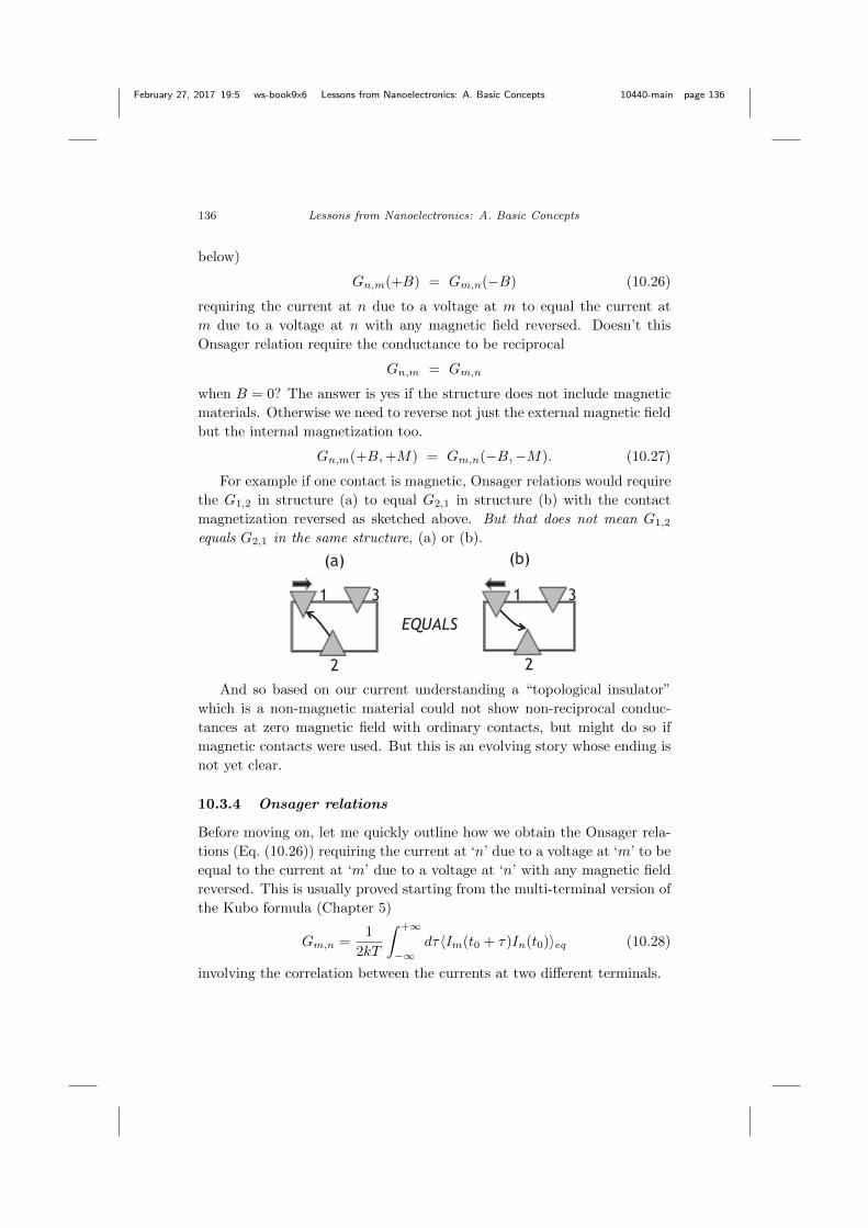
February 27, 2017 19:5 ws-book9x6 Lessons from Nanoelectronics: A. Basic Concepts 10440-main page 136
136 Lessons from Nanoelectronics: A. Basic Concepts
below)
Gn,m(+B) = Gm,n(−B) (10.26)
requiring the current at n due to a voltage at m to equal the current at
m due to a voltage at n with any magnetic field reversed. Doesn’t this
Onsager relation require the conductance to be reciprocal
Gn,m = Gm,n
when B = 0? The answer is yes if the structure does not include magnetic
materials. Otherwise we need to reverse not just the external magnetic field
but the internal magnetization too.
Gn,m(+B,+M) = Gm,n(−B,−M). (10.27)
For example if one contact is magnetic, Onsager relations would require
the G1,2 in structure (a) to equal G2,1 in structure (b) with the contact
magnetization reversed as sketched above. But that does not mean G1,2
equals G2,1 in the same structure, (a) or (b).
1
2
3
(b)
EQUALS
1
2
3
(a)
And so based on our current understanding a “topological insulator”
which is a non-magnetic material could not show non-reciprocal conduc-
tances at zero magnetic field with ordinary contacts, but might do so if
magnetic contacts were used. But this is an evolving story whose ending is
not yet clear.
10.3.4 Onsager relations
Before moving on, let me quickly outline how we obtain the Onsager rela-
tions (Eq. (10.26)) requiring the current at ‘n’ due to a voltage at ‘m’ to be
equal to the current at ‘m’ due to a voltage at ‘n’ with any magnetic field
reversed. This is usually proved starting from the multi-terminal version of
the Kubo formula (Chapter 5)
Gm,n =1
2kT
∫ +∞
−∞dτ〈Im(t0 + τ)In(t0)〉eq (10.28)
involving the correlation between the currents at two different terminals.
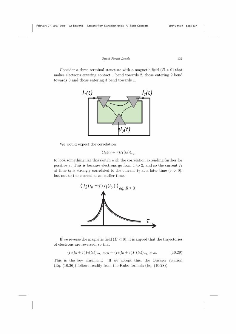
February 27, 2017 19:5 ws-book9x6 Lessons from Nanoelectronics: A. Basic Concepts 10440-main page 137
Quasi-Fermi Levels 137
Consider a three terminal structure with a magnetic field (B > 0) that
makes electrons entering contact 1 bend towards 2, those entering 2 bend
towards 3 and those entering 3 bend towards 1.
1(t) 2(t)
3(t)
We would expect the correlation
〈I2(t0 + τ)I1(t0)〉eq
to look something like this sketch with the correlation extending further for
positive τ . This is because electrons go from 1 to 2, and so the current I1at time t0 is strongly correlated to the current I2 at a later time (τ > 0),
but not to the current at an earlier time.
I2(t0 + ) I1(t0 ) eq, B > 0
If we reverse the magnetic field (B < 0), it is argued that the trajectories
of electrons are reversed, so that
〈I1(t0 + τ)I2(t0)〉eq, B<0 = 〈I2(t0 + τ)I1(t0)〉eq, B>0. (10.29)
This is the key argument. If we accept this, the Onsager relation
(Eq. (10.26)) follows readily from the Kubo formula (Eq. (10.28)).

February 27, 2017 19:5 ws-book9x6 Lessons from Nanoelectronics: A. Basic Concepts 10440-main page 138
138 Lessons from Nanoelectronics: A. Basic Concepts
What we have discussed here is really the simplest of the Onsager re-
lations for the generalized transport coefficients relating generalized forces
to fluxes. For example, in Chapter 13 we will discuss additional coeffi-
cients like GS relating a temperature difference to the electrical current.
There are generalized Onsager relations that require (at zero magnetic
field) GP = TGS , GP being the coefficient relating the heat current to
the potential difference.
This is of course not obvious and requires deep and profound arguments
that have prompted some to call the Onsager relations the fourth law of
thermodynamics (see for example, Yourgrau et al. 1966). Interestingly,
however, in Chapter 13 we will obtain transport coefficients that satisfy
this relation GP = TGS straightforwardly (see Eqs. (13.6) and (13.17a))
without any profound or subtle arguments.
We could cite this as one more example of the power and simplicity of
the elastic resistor that comes from disentangling mechanics from thermo-
dynamics.

February 27, 2017 19:5 ws-book9x6 Lessons from Nanoelectronics: A. Basic Concepts 10440-main page 139
Chapter 11
Hall Effect
11.1 Introduction
Let me briefly explain what the Hall effect is about. Consider a two-
dimensional conductor (see Fig. 11.1) carrying current, subject to a per-
pendicular magnetic field along the y-direction which exerts a force on the
electrons perpendicular to its velocity.
F =dp
dt= −qv ×B. (11.1)
Source Drain
VI
zx
Electron Current
Fig. 11.1 A magnetic field B in the y-direction makes electrons from the source veer“up”wards.
This would cause an electron from the source to veer “up”wards and
an electron from the drain to veer “down”wards as shown. Since there are
more electrons headed from source to drain, we expect electrons to pile up
on the top side causing a voltage VH to develop in the x-direction transverse
to current flow (see Fig. 11.2).
139
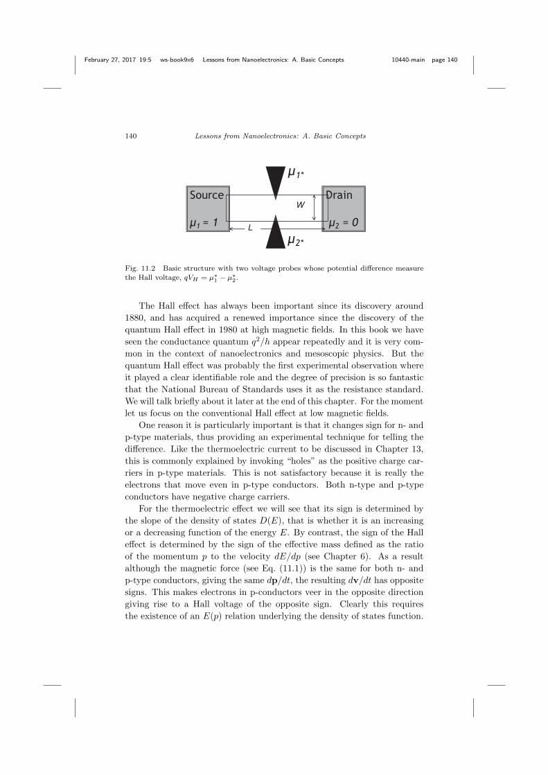
February 27, 2017 19:5 ws-book9x6 Lessons from Nanoelectronics: A. Basic Concepts 10440-main page 140
140 Lessons from Nanoelectronics: A. Basic Concepts
Source
µ1 = 1
Drain
µ2 = 0
µ1*
µ2*
D
Fig. 11.2 Basic structure with two voltage probes whose potential difference measure
the Hall voltage, qVH = µ∗1 − µ∗2.
The Hall effect has always been important since its discovery around
1880, and has acquired a renewed importance since the discovery of the
quantum Hall effect in 1980 at high magnetic fields. In this book we have
seen the conductance quantum q2/h appear repeatedly and it is very com-
mon in the context of nanoelectronics and mesoscopic physics. But the
quantum Hall effect was probably the first experimental observation where
it played a clear identifiable role and the degree of precision is so fantastic
that the National Bureau of Standards uses it as the resistance standard.
We will talk briefly about it later at the end of this chapter. For the moment
let us focus on the conventional Hall effect at low magnetic fields.
One reason it is particularly important is that it changes sign for n- and
p-type materials, thus providing an experimental technique for telling the
difference. Like the thermoelectric current to be discussed in Chapter 13,
this is commonly explained by invoking “holes” as the positive charge car-
riers in p-type materials. This is not satisfactory because it is really the
electrons that move even in p-type conductors. Both n-type and p-type
conductors have negative charge carriers.
For the thermoelectric effect we will see that its sign is determined by
the slope of the density of states D(E), that is whether it is an increasing
or a decreasing function of the energy E. By contrast, the sign of the Hall
effect is determined by the sign of the effective mass defined as the ratio
of the momentum p to the velocity dE/dp (see Chapter 6). As a result
although the magnetic force (see Eq. (11.1)) is the same for both n- and
p-type conductors, giving the same dp/dt, the resulting dv/dt has opposite
signs. This makes electrons in p-conductors veer in the opposite direction
giving rise to a Hall voltage of the opposite sign. Clearly this requires
the existence of an E(p) relation underlying the density of states function.
February 27, 2017 19:5 ws-book9x6 Lessons from Nanoelectronics: A. Basic Concepts 10440-main page 141
Hall Effect 141
Perhaps it is for this reason that amorphous semiconductors which lack a
well-defined E(p) often show strange results for the Hall effect and yet show
reasonable thermoelectric effect.
The simple theory of the Hall effect given in freshman physics texts goes
like this. First the current is written as
I = q(N/L)vd (11.2)
with the drift velocity given by the product of the mobility and the electric
field in the z-direction:
vd = µ (V/L). (11.3)
These two relations are normally combined to yield the Drude formula (see
Eq. (6.1))
I
V= q
N
WLµ︸ ︷︷ ︸
σ
W
L. (11.4)
For the Hall effect, it is argued that an electric field VH/W must appear in
the x-direction to offset the magnetic force
VHW
= vdB. (11.5)
Combining Eq. (11.5) with Eq. (11.2) one obtains the standard expression
for the Hall resistance
RH =VHI
=B
q(N/LW ). (11.6)
One reason the Hall effect is widely used is that Eq. (11.6) allows us to
determine the electron density N/LW from the slope of the Hall resistance
versus B-field curve. This looks like a straightforward transparent theory
for a well-established effect. What more could we add to it?
The main concern we have about this derivation is the same concern
that we voiced regarding the Drude formula, namely that if electric field
were indeed what drives currents then all electrons should feel its effect.
Indeed Eq. (11.6) for the Hall resistance conveys the impression that the
Hall effect depends on the total electron density N/LW over all energies.
But we believe this is not correct.
Like the other transport coefficients we have discussed, the Hall resis-
tance too is a “Fermi surface property” that depends only on the electrons

February 27, 2017 19:5 ws-book9x6 Lessons from Nanoelectronics: A. Basic Concepts 10440-main page 142
142 Lessons from Nanoelectronics: A. Basic Concepts
in an energy window ∼ a few kT around E = µ0 and not on the total num-
ber of electrons obtained by integrating over energy. We will show that the
Hall resistance for a single energy channel of an elastic resistor is given by
RH(E) =2BLW
qD(E)v(E)p(E)(11.7)
which can be averaged over an energy window ∼ of a few kT around E = µ0
using our standard broadening function:
1
RH=
∫ +∞
−∞dE
(− ∂f0
∂E
)1
RH(E). (11.8)
Note that in general we should integrate the conductance 1/RH rather
than the resistance RH since different energy channels all have the same
voltage so that they conduct “in parallel” as circuit experts would put
it. Equations (11.8) and (11.7) can be reduced to the standard result
(Eq. (11.6)) by making use of the single band relation obtained in Chapter 6
D(E)v(E)p(E) = N(E) · d (same as Eq. (6.9))
with d = 2 for a two-dimensional conductor and relating the average of
N(E) to the total number of electrons as we did in Section 6.5.
But if the single band relation (Eq. (6.9)) is not applicable one should
use the expression in Eq. (11.8) rather than Eq. (11.6). In any case,
Eq. (11.8) shows that the effect really does not involve electrons at all
energies. One reason this point causes some confusion is the existence of
equilibrium currents inside the sample in the presence of a magnetic field
which involve all electrons at all energies.
However, these are dissipationless currents of the type that exist even
if we put a hydrogen atom in a magnetic field and have nothing to do with
the transport coefficients we are talking about. In any transport model it
1 = 0 2 = 0
EquilibriumCurrents
Fig. 11.3 Equilibrium currents can exist in any conductor in the presence of a magneticfield.

February 27, 2017 19:5 ws-book9x6 Lessons from Nanoelectronics: A. Basic Concepts 10440-main page 143
Hall Effect 143
is important to eliminate these non Fermi surface currents. A similar issue
arises with respect to spin currents even without any magnetic fields (which
we will discuss in Part B).
Getting back to the problem of determining the Hall voltage, as we saw
in Chapter 10 there are two approaches: (a) calculate the non-equilibrium
electrochemical potential inside the conductor or (b) treat it as a four termi-
nal structure using the Buttiker equation. We will not discuss the second
one here since the basic idea was already discussed at the end of Chap-
ter 10. Instead we will focus on the first approach which gives insights into
the variation of the electrochemical potential inside the channel. But first
let us briefly discuss the dynamics of electrons in a B-field.
11.2 Why n- and p-type Conductors are Different
μ0
D(E)
N(E)
D(E)
E E
N(E)
Fig. 11.4 The Hall resistance changes sign for n- and p-type conductors and is inversely
proportional to N(E) at E = µ0.
Why do n- and p-type conductors show opposite signs of the Hall effect?
The basic difference is that in n-type conductors, the velocity is parallel
to the momentum, while in p-type conductors, it is anti-parallel because
v = dE/dp, and in p-type conductors the energy decreases with increasing
p (Fig. 11.4). To see why the relative sign of p and v matters, let us consider
the magnetic force described by Eq. (11.1) in a little more detail.

February 27, 2017 19:5 ws-book9x6 Lessons from Nanoelectronics: A. Basic Concepts 10440-main page 144
144 Lessons from Nanoelectronics: A. Basic Concepts
z
x
For any isotropic E(p) relation, the velocity and momentum are collinear
(parallel or anti-parallel) pointing, say at an angle θ to the z-axis, so that
p = p cos θ z + p sin θ x
v = v cos θ z + v sin θ x.
Inserting into Eq. (11.1) we obtain
dθ
dt=
qvB
p(11.9)
showing that the angle θ increases linearly with time so that the velocity
and momentum vectors rotate uniformly in the z-x plane. But the sense of
rotation is opposite for n- and p-type conductors because the ratio p/v has
opposite signs. This is the ratio we defined as mass (see Eq. (6.11)) and is
constant for parabolic dispersion (Eq. (6.12)).
ωc =
∣∣∣∣qvBp∣∣∣∣E=µ0
=
∣∣∣∣qBm∣∣∣∣E=µ0
. (11.10)
But for a linear dispersion (Eq. (6.13)) the mass increases with energy,
so that the cyclotron frequency decreases with increased carrier density, as
is observed in graphene. The magnetic field tries to make the electron go
round and round in a circle with an angular frequency ωc. However, it
gets scattered after a mean free time τ , so that if ωcτ 1 the electron
never really gets to complete a full rotation. This is the low field regime
where the Hall resistance in given by Eq. (11.6), while the high field regime
characterized by ωcτ 1 leads to the quantum Hall effect mentioned ear-
lier. Let us now discuss our first approach to the problem of determining
the Hall resistance (Eq. (11.7)) based on looking at the non-equilibrium
electrochemical potentials inside the conductor.

February 27, 2017 19:5 ws-book9x6 Lessons from Nanoelectronics: A. Basic Concepts 10440-main page 145
Hall Effect 145
11.3 Spatial Profile of Electrochemical Potential
As I mentioned earlier, the textbook derivation of the Hall resistance
(Eq. (11.6)) looks fairly straightforward, but we are attempting to pro-
vide a different expression (Eq. (11.7)) motivated by the same reasons that
prompted us to describe an alternative expression for the conductivity back
in Chapter 6.
In our elastic resistor model, the role of the drift velocity in the text-
book derivation is played by the potential separation
δµ = µ+ − µ−
between drainbound and sourcebound states, so that instead of Eq. (11.2)
we have (see Eq. (8.23))
I(E) =q
hM(E)
(−∂f0
∂E
)δµ (11.11)
withM(E)
h=
D(E)v(E)
πL(11.12)
where we have used the result for 2D conductors from Eq. (4.13).
Instead of Eq. (11.3), we have the potential separation related to the
applied voltage by
δµ =qV λ
L+ λ∼= qV
λ
L. (11.13)
This relation can be obtained by noting that δµ is equal to the fraction
of the applied qV that is dropped across the interface resistance RB (see
Fig. 8.2):
δµ = qVRBR
= qVG
GB.
Making use of Eq. (4.5a) we obtain Eq. (11.13).
Just as Eqs. (11.2) and (11.3) yield the Drude expression for the con-
ductivity, similarly Eqs. (11.11) and (11.13) can be combined to yield the
more general conductivity expression discussed earlier (see Eq. (6.5)).
For the Hall effect we also need a replacement for Eq. (11.5)
VHW
= vd B
which we will show is given by
VHW
=2
π
δµ
pB (11.14)

February 27, 2017 19:5 ws-book9x6 Lessons from Nanoelectronics: A. Basic Concepts 10440-main page 146
146 Lessons from Nanoelectronics: A. Basic Concepts
Eq. (11.14) together with Eqs. (11.11) and (11.13) gives us the result for Hall
resistance stated earlier in Eq. (11.7). Unfortunately we do not have a one-
line argument for Eq. (11.14) like the one used for Eq. (11.5). Instead I need
to describe a two-page argument using the BTE discussed in Chapter 9.
Source
1
Drain
2
1*
2*
L
W
x
z
+1
2
-qV
μ
Fig. 11.5 Spatial variation of µ± along z.
11.3.1 Obtaining Eq. (11.14) from BTE
Back in Chapter 9 we obtained a solution for a subset of this problem based
on a solution of
vz∂µ
∂z= −µ− µ
τ(11.15)
and obtained the solutions for the electrochemical potentials µ+ and µ−
sketched above in Fig. 11.5. The solutions could be written in the form
µ(z, θ) = µ(z) +2
πδµ cos θ (11.16)
where we have separated out a z-dependent part µ from the momentum-
dependent part at a specific location, z. The latter needs a little discussion.
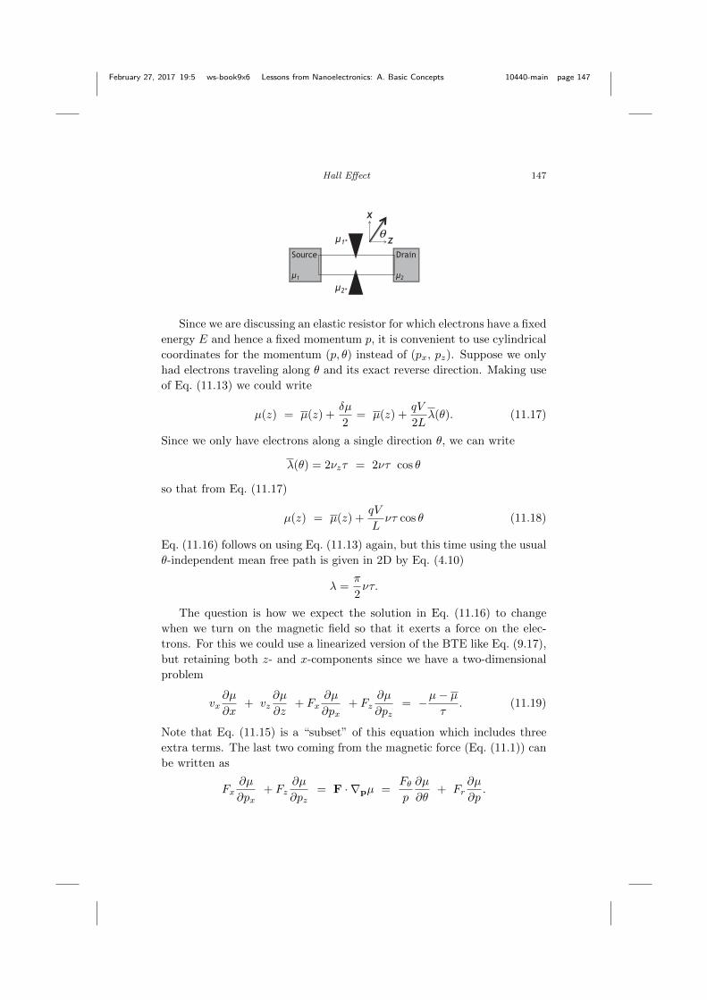
February 27, 2017 19:5 ws-book9x6 Lessons from Nanoelectronics: A. Basic Concepts 10440-main page 147
Hall Effect 147
Source
µ1
Drain
µ2
µ1*
µ2*
z
x
Since we are discussing an elastic resistor for which electrons have a fixed
energy E and hence a fixed momentum p, it is convenient to use cylindrical
coordinates for the momentum (p, θ) instead of (px, pz). Suppose we only
had electrons traveling along θ and its exact reverse direction. Making use
of Eq. (11.13) we could write
µ(z) = µ(z) +δµ
2= µ(z) +
qV
2Lλ(θ). (11.17)
Since we only have electrons along a single direction θ, we can write
λ(θ) = 2νzτ = 2ντ cos θ
so that from Eq. (11.17)
µ(z) = µ(z) +qV
Lντ cos θ (11.18)
Eq. (11.16) follows on using Eq. (11.13) again, but this time using the usual
θ-independent mean free path is given in 2D by Eq. (4.10)
λ =π
2ντ.
The question is how we expect the solution in Eq. (11.16) to change
when we turn on the magnetic field so that it exerts a force on the elec-
trons. For this we could use a linearized version of the BTE like Eq. (9.17),
but retaining both z- and x-components since we have a two-dimensional
problem
vx∂µ
∂x+ vz
∂µ
∂z+ Fx
∂µ
∂px+ Fz
∂µ
∂pz= −µ− µ
τ. (11.19)
Note that Eq. (11.15) is a “subset” of this equation which includes three
extra terms. The last two coming from the magnetic force (Eq. (11.1)) can
be written as
Fx∂µ
∂px+ Fz
∂µ
∂pz= F · ∇pµ =
Fθp
∂µ
∂θ+ Fr
∂µ
∂p.
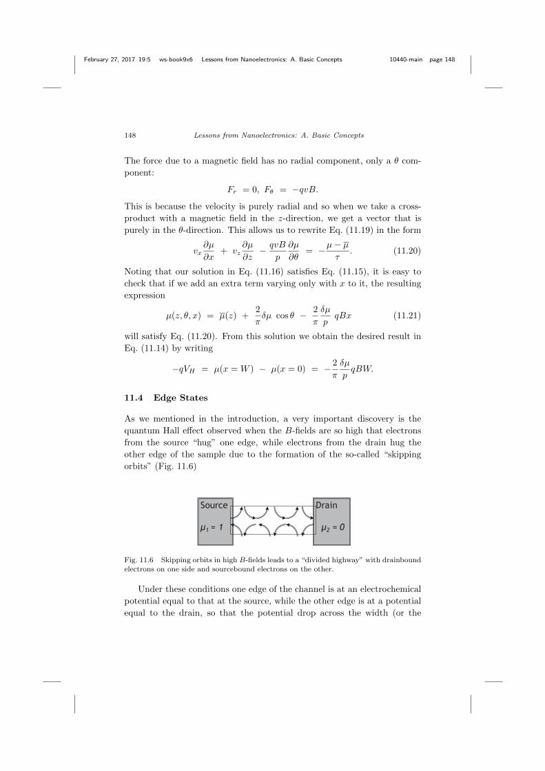
February 27, 2017 19:5 ws-book9x6 Lessons from Nanoelectronics: A. Basic Concepts 10440-main page 148
148 Lessons from Nanoelectronics: A. Basic Concepts
The force due to a magnetic field has no radial component, only a θ com-
ponent:
Fr = 0, Fθ = −qvB.
This is because the velocity is purely radial and so when we take a cross-
product with a magnetic field in the z-direction, we get a vector that is
purely in the θ-direction. This allows us to rewrite Eq. (11.19) in the form
vx∂µ
∂x+ vz
∂µ
∂z− qvB
p
∂µ
∂θ= −µ− µ
τ. (11.20)
Noting that our solution in Eq. (11.16) satisfies Eq. (11.15), it is easy to
check that if we add an extra term varying only with x to it, the resulting
expression
µ(z, θ, x) = µ(z) +2
πδµ cos θ − 2
π
δµ
pqBx (11.21)
will satisfy Eq. (11.20). From this solution we obtain the desired result in
Eq. (11.14) by writing
−qVH = µ(x = W ) − µ(x = 0) = − 2
π
δµ
pqBW.
11.4 Edge States
As we mentioned in the introduction, a very important discovery is the
quantum Hall effect observed when the B-fields are so high that electrons
from the source “hug” one edge, while electrons from the drain hug the
other edge of the sample due to the formation of the so-called “skipping
orbits” (Fig. 11.6)
Source
µ1 = 1
Drain
µ2 = 0
Fig. 11.6 Skipping orbits in high B-fields leads to a “divided highway” with drainbound
electrons on one side and sourcebound electrons on the other.
Under these conditions one edge of the channel is at an electrochemical
potential equal to that at the source, while the other edge is at a potential
equal to the drain, so that the potential drop across the width (or the

February 27, 2017 19:5 ws-book9x6 Lessons from Nanoelectronics: A. Basic Concepts 10440-main page 149
Hall Effect 149
Hall voltage) is equal to that between the source and the drain. This is
very different from the ordinary Hall effect when the Hall voltage given
by Eq. (11.14) is a small fraction of the applied voltage. What makes
the quantum Hall effect so extraordinary is that the Hall resistance (Hall
voltage divided by the current) is given by
R =h
q2 i(11.22)
where i is an integer to a fantastic degree of precision, making this a re-
sistance standard used by the National Bureau of Standards. It is as if we
have an unbelievably perfect ballistic conductor whose only resistance is
the interface resistance.
Since these conductors are often hundreds of micrometers long, this per-
fect ballisticity is amazing and was recognized with a Nobel prize in 1985
(von Klitzing K. et al. 1980). One can ascribe this incredible ballisticity to
the formation of a “divided” electronic highway (Fig. 11.6) with drainbound
electrons so well-separated from the sourcebound electrons that backscat-
tering is extremely unlikely (Fig. 11.6). This simple picture, however, is a
little too simple. It does not for example tell us the significance of the in-
teger i in Eq. (11.22) which requires some input from quantum mechanics,
as we will see in Part B.

February 27, 2017 19:5 ws-book9x6 Lessons from Nanoelectronics: A. Basic Concepts 10440-main page 150
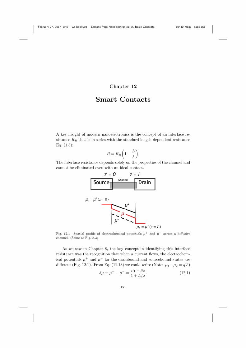
February 27, 2017 19:5 ws-book9x6 Lessons from Nanoelectronics: A. Basic Concepts 10440-main page 151
Chapter 12
Smart Contacts
A key insight of modern nanoelectronics is the concept of an interface re-
sistance RB that is in series with the standard length-dependent resistance
Eq. (1.8):
R = RB
(1 +
L
λ
).
The interface resistance depends solely on the properties of the channel and
cannot be eliminated even with an ideal contact.
μ2 = μ (z = L)
μ1 = μ+ (z = 0)
µ+
µ-
µ
z = 0 z = LSource Drain
Fig. 12.1 Spatial profile of electrochemical potentials µ+ and µ− across a diffusive
channel. (Same as Fig. 8.3)
As we saw in Chapter 8, the key concept in identifying this interface
resistance was the recognition that when a current flows, the electrochem-
ical potentials µ+ and µ− for the drainbound and sourcebound states are
different (Fig. 12.1). From Eq. (11.13) we could write (Note: µ1−µ2 = qV )
δµ ≡ µ+ − µ− =µ1 − µ2
1 + L/λ. (12.1)
151
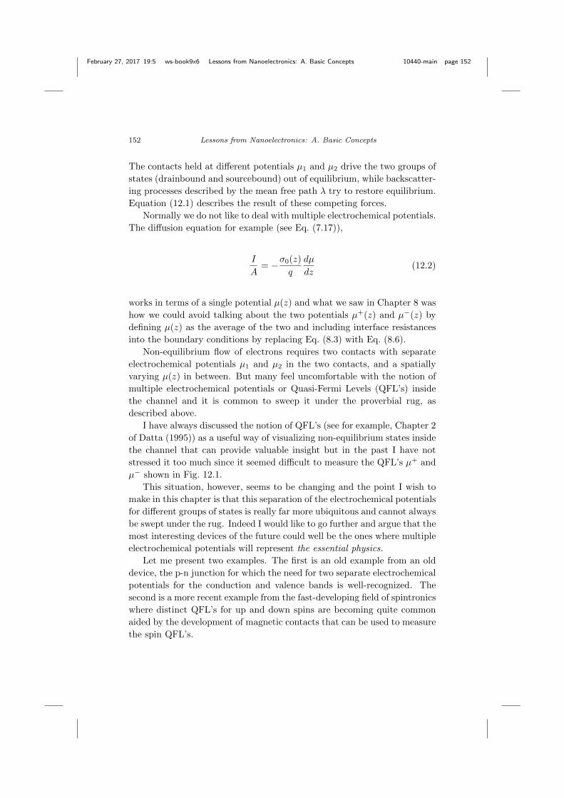
February 27, 2017 19:5 ws-book9x6 Lessons from Nanoelectronics: A. Basic Concepts 10440-main page 152
152 Lessons from Nanoelectronics: A. Basic Concepts
The contacts held at different potentials µ1 and µ2 drive the two groups of
states (drainbound and sourcebound) out of equilibrium, while backscatter-
ing processes described by the mean free path λ try to restore equilibrium.
Equation (12.1) describes the result of these competing forces.
Normally we do not like to deal with multiple electrochemical potentials.
The diffusion equation for example (see Eq. (7.17)),
I
A= −σ0(z)
q
dµ
dz(12.2)
works in terms of a single potential µ(z) and what we saw in Chapter 8 was
how we could avoid talking about the two potentials µ+(z) and µ−(z) by
defining µ(z) as the average of the two and including interface resistances
into the boundary conditions by replacing Eq. (8.3) with Eq. (8.6).
Non-equilibrium flow of electrons requires two contacts with separate
electrochemical potentials µ1 and µ2 in the two contacts, and a spatially
varying µ(z) in between. But many feel uncomfortable with the notion of
multiple electrochemical potentials or Quasi-Fermi Levels (QFL’s) inside
the channel and it is common to sweep it under the proverbial rug, as
described above.
I have always discussed the notion of QFL’s (see for example, Chapter 2
of Datta (1995)) as a useful way of visualizing non-equilibrium states inside
the channel that can provide valuable insight but in the past I have not
stressed it too much since it seemed difficult to measure the QFL’s µ+ and
µ− shown in Fig. 12.1.
This situation, however, seems to be changing and the point I wish to
make in this chapter is that this separation of the electrochemical potentials
for different groups of states is really far more ubiquitous and cannot always
be swept under the rug. Indeed I would like to go further and argue that the
most interesting devices of the future could well be the ones where multiple
electrochemical potentials will represent the essential physics.
Let me present two examples. The first is an old example from an old
device, the p-n junction for which the need for two separate electrochemical
potentials for the conduction and valence bands is well-recognized. The
second is a more recent example from the fast-developing field of spintronics
where distinct QFL’s for up and down spins are becoming quite common
aided by the development of magnetic contacts that can be used to measure
the spin QFL’s.

February 27, 2017 19:5 ws-book9x6 Lessons from Nanoelectronics: A. Basic Concepts 10440-main page 153
Smart Contacts 153
12.1 p-n Junctions
Figure 12.2 shows a grayscale plot of the density of states D(z, E). The
white band indicates the bandgap with a non-zero DOS both above and
below it on each side which are shifted in energy with respect to each
other. A positive voltage is applied to the right with respect to the left, so
that µ2 is lower than µ1 as shown.
1
E
z
2
Fig. 12.2 Simplified grayscale plot of the spatially varying density of states D(z, E)
across a p-n junction.
If we look at a narrow range of energies around µ1 it communicates
primarily with contact 1. If we look at a narrow range of energies around
µ2 it communicates primarily with contact 2. We could draw an idealized
diagram with each of these two groups communicating just with one contact
and cut off from the other as shown in Fig. 12.3. In reality of course neither
group is completely cutoff from either contact, and people who design real
devices often go to great lengths to achieve better isolation, but let us not
worry about such details.
Would the idealized device in Fig. 12.3 allow any current to flow? None
at all, if it were an elastic resistor. There is no energy channel that will let
an electron get all the way from left to right. The ones connected to the
left are disconnected from the right and those connected to the right are
disconnected from the left.
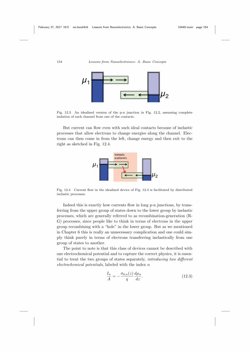
February 27, 2017 19:5 ws-book9x6 Lessons from Nanoelectronics: A. Basic Concepts 10440-main page 154
154 Lessons from Nanoelectronics: A. Basic Concepts
μ1μ2
Fig. 12.3 An idealized version of the p-n junction in Fig. 12.2, assuming complete
isolation of each channel from one of the contacts.
But current can flow even with such ideal contacts because of inelastic
processes that allow electrons to change energies along the channel. Elec-
trons can then come in from the left, change energy and then exit to the
right as sketched in Fig. 12.4.
Inelastic scatterers
μ1μ2
Fig. 12.4 Current flow in the idealized device of Fig. 12.3 is facilitated by distributedinelastic processes.
Indeed this is exactly how currents flow in long p-n junctions, by trans-
ferring from the upper group of states down to the lower group by inelastic
processes, which are generally referred to as recombination-generation (R-
G) processes, since people like to think in terms of electrons in the upper
group recombining with a “hole” in the lower group. But as we mentioned
in Chapter 6 this is really an unnecessary complication and one could sim-
ply think purely in terms of electrons transferring inelastically from one
group of states to another.
The point to note is that this class of devices cannot be described with
one electrochemical potential and to capture the correct physics, it is essen-
tial to treat the two groups of states separately, introducing two different
electrochemical potentials, labeled with the index n
InA
= −σ0,n(z)
q
dµndz
. (12.3)

February 27, 2017 19:5 ws-book9x6 Lessons from Nanoelectronics: A. Basic Concepts 10440-main page 155
Smart Contacts 155
These currents are all coupled together by inelastic processes generally
called recombination-generation or “RG” processes in the context of p-n
junctions
dIndz
=∑m
(RGm→n −RGn→m
)(12.4)
that take electrons from one group of states m to the other n. This is
indeed the way p-n junctions are modeled.
It is well-known that the current in a p-n junction is given by an ex-
pression of the form
I = I0(eqV/νkT − 1
)(12.5)
where the number ν as well as the coefficient I0 are determined by the
nature of the inelastic or RG processes. The conductivities of either of the
two groups of states play hardly any role in determining this current.
The physical reason for this is clear. The rate-determining step in cur-
rent flow is the inelastic process transferring electrons from one group of
states to the other. Transport within any of these groups only adds an
unimportant resistance in series with the basic device.
Everything we have talked about in this book has been about the con-
ductivities σn of the homogeneous p-type or n-type materials. And this is
exactly the physics that is relevant to the operation of the most popular
electronic device today, namely the Field Effect Transistor (FET) whose
conductivity is controlled by a gate electrode through the electrostatic po-
tential U .
But the p-n junction is a totally different device from the FET both in
terms of its current-voltage characteristics and the physics that underlies
it. It is the basic device structure used to construct solar cells and the
principle it embodies is key to a broad class of energy conversion devices.
So let me take a short detour to elaborate on this principle.
12.1.1 Current-voltage characteristics
Consider for example the device in Fig. 12.5 assuming that the upper group
of states (labeled A) is clustered around an energy εA while the lower group
(labeled B) is clustered around εB .

February 27, 2017 19:5 ws-book9x6 Lessons from Nanoelectronics: A. Basic Concepts 10440-main page 156
156 Lessons from Nanoelectronics: A. Basic Concepts
μ1μ2
A
B
Fig. 12.5 Same as Fig. 12.4 with the two groups of states labeled A and B. Electronic
transitions between A and B are facilitated by inelastic interactions.
The essential physics of such p-n junction like devices is contained not
in Eq. (12.3), but in Eq. (12.4) which for two levels A and B can be written
as
I ∼ DBAfA(εA)(
1− fB(εB))−DABfB
(εB)(
1− fA(εA))
(12.6)
where the coefficients DBA and DAB denote the strength of the inelastic
processes inducing the transitions from A to B and from B to A respectively
(note that the transition occurs from the second subscript to the first).
Interestingly these two rates DAB and DBA are generally NOT equal.
DAB involves absorbing an amount of energy
~ω = εA − εB
from the surroundings, while DBA involves giving up the same amount of
energy.
A fundamental principle of equilibrium statistical mechanics (see Chap-
ter 15) is that if the entity causing the inelastic scattering is at equilibrium
with a temperature T0, then it is always harder to absorb energy from it
than it is to give up energy to it and the ratio of the two processes is given
by
DAB
DBA= exp
(− ~ωkT0
). (12.7)
We can write the current from Eq. (12.6) in the form
I ∼ DABfB(εB)(
1− fA(εA))(
X − 1
)(12.8)
where X ≡ DBA
DAB
fA(εA)
1− fA(εA) 1− fB
(εB)
fB(εB) . (12.9)
February 27, 2017 19:5 ws-book9x6 Lessons from Nanoelectronics: A. Basic Concepts 10440-main page 157
Smart Contacts 157
Making use of Eqs. (12.8) and (12.9) and the following property of Fermi
functions (Eq. (2.2))
1− f0
(ε)
f0
(ε) = exp
(ε− µ0
kT
)(12.10)
we can rewrite Eq. (12.9) as
X = exp
(~ωkT0− ~ωkT
)exp
(µA − µBkT
). (12.11)
Since Level A is connected to contact 1 and Level B to contact 2, if the
inelastic processes taking electrons from A to B are not too strong, level A
is almost in equilibrium with contact 1 and level B with contact 2, so that
µA − µB ≈ µ1 − µ2 = qV.
If T0 = T , we can write the current from Eq. (12.8) as
I ∼(X − 1
)∼ eqV/kT − 1
which is the ideal I-V relation for p-n junctions stated earlier (see
Eq. (12.5)) with ν = 1. Other values of ν are also obtained in practice
but that requires a more detailed discussion beyond the scope of this book.
The more important point I want to stress is that this device can be
used for energy conversion. If the scatterers are at a temperature different
from that of the device (T0 6= T ) then one can have a current flowing even
without any applied voltage. This short circuit current is given by
Isc ≡ I(V = 0) ∼ exp
~ωk
(1
T0− 1
T
)− 1. (12.12)
One could in principle use a device like this to convert a temperature
difference (T0 6= T ) into an electrical current. The short circuit current
has the opposite sign for T0 > T and for T > T0. Readers familiar with
Feynman’s ratchet and pawl lecture (Feynman 1963, cited in Chapter 15)
may notice the similarity. The ratchet reverses direction depending on
whether its temperature is lower or higher than the ambient.
One could view more practical devices like solar cells as embodi-
ments of the same principle, the light from the sun having a temperature
T0 ∼ 6000C characteristic of the surface of the sun, much larger than the
ambient temperature.
From Eq. (12.8) it is easy to see that under open circuit conditions
(I = 0), we must have X = 1, so that from Eq. (12.11) we have
qVOC~ω
= 1− T
T0.

February 27, 2017 19:5 ws-book9x6 Lessons from Nanoelectronics: A. Basic Concepts 10440-main page 158
158 Lessons from Nanoelectronics: A. Basic Concepts
The left hand side represents the energy extracted per photon under very
low current (near open circuit) conditions, so that this could be called the
Carnot efficiency of a solar cell viewed as a “heat engine”. However, since
T0 T , this Carnot efficiency is very close to 100% and my colleague
Ashraf often points out that other factors related to the small angular
spectrum of solar energy are important in lowering the ideal efficiency to
much lower values.
12.1.2 Contacts are fundamental
μ1μ2
A
B
e-e-
(a)
μ1 μ2
(b)
Fig. 12.6 (a) Asymmetric contacts are central to the operation of the “solar cell”. (b) If
contacted symmetrically no electrical output is obtained.
The point I want to make is how important the discriminating contacts are
in the design of this class of devices which we could generally refer to as
“solar cells” (Fig. 12.6a). The external source raises electrons from the B
states to the A states from where they exit through the left contact, while
the empty state left behind in B is filled up by an electron that comes in
through the right contact. Every electron raised from B to A thus causes
an electron to flow in the external circuit.
But if the contacts are connected “normally” injecting and extracting
equally from either group (Fig. 12.6b) then we cannot expect any current
to flow in the external circuit, from the sheer symmetry of the arrangement.
After all, why should electrons flow from left to right any more that they
would flow from right to left?
It is this asymmetric contacting that makes p-n junctions fundamen-
tally different from the Field Effect Transistor (FET) that we started our
chapters with, both in terms of the current-voltage characteristics and the
physics underlying it. It is of course well recognized that the physics of p-n
junctions demands two different electrochemical potentials. What is not as
well recognized is the generic nature of this phenomenon. Let us now look
at a more recent example.

February 27, 2017 19:5 ws-book9x6 Lessons from Nanoelectronics: A. Basic Concepts 10440-main page 159
Smart Contacts 159
12.2 Spin Potentials
Related video lecture available at course website, Unit 3: L3.9.
12.2.1 Spin valve
One of the major developments in the last two decades is the spin valve, a
device with two magnetic contacts (Fig. 12.7). If they are magnetized in the
same direction (parallel configuration, P) the resulting resistance is lower
than if they are magnetized in opposite directions (anti-parallel configura-
tion, AP). Since its first demonstration in 1988, it rapidly found application
as a “reading” device to sense the information stored in a magnetic memory
and the discovery was recognized with a Nobel prize in 2007.
(a) Parallel (P)
rr Rch
RR Rch
(b) Anti-Parallel (AP)
R
r
r
R
Rch
Rch
Fig. 12.7 Spin valve: (a) Parallel (P) configuration. (b) Anti-parallel (AP) configura-
tion.
So far we have only mentioned spin as part of a “degeneracy factor, g”
(Section 6.4.1), the idea being that electronic states always come in pairs,
one corresponding to each spin. We could call these “up” and “down” or
“left” and “right” or even “red” and “blue” as we have done in Fig. (12.7).
Note that the two spins are not spatially separated even though we have
separated the red and the blue channel for clarity. Ordinarily, the two
channels are identical and we can calculate the conductance due to one and
remember to multiply by two.
But in spin valve devices the contacts are magnets that treat the two
February 27, 2017 19:5 ws-book9x6 Lessons from Nanoelectronics: A. Basic Concepts 10440-main page 160
160 Lessons from Nanoelectronics: A. Basic Concepts
spin channels differently and the operation of a spin valve can be understood
in fairly simple terms if we postulate that each spin channel has a different
interface resistance with the magnet depending on whether it is parallel
(majority spin) or anti-parallel (minority spin) to the magnetization.
If we assume the interface resistance for majority spins to be r and for
minority spins to be R (r < R) we can draw simple circuit representations
for the P and AP configurations as shown, with Rch representing the chan-
nel resistance. Elementary circuit theory then gives us the resistance for
the parallel configuration as
RP =
(1
2r +Rch+
1
2R+Rch
)−1
(12.13)
and that for the anti-parallel configuration as
RAP =r +R+Rch
2. (12.14)
The essence of the spin valve device is the difference between RP and
RAP and we would expect this to be most pronounced when the channel
resistance is negligible and everything is dominated by the interfaces. We
obtain a simple result for the maximum magnetoresistance or MR if we set
Rch = 0
MR ≡ RAPRP
− 1 =(R− r)2
4rR(12.15)
which can be written in terms of the polarization:
P ≡ R− rR+ r
(12.16a)
MR =P 2
1− P 2. (12.16b)
I should mention here that the expression commonly seen in the literature
has an extra factor of 2 compared to Eq. (12.16b)
MR =2P 2
1− P 2
which is applicable to magnetic tunnel junctions (MTJ’s) that use short
tunnel junctions as channels instead of the metallic channels we have been
discussing. We get this extra factor of 2, if we assume that two resistors
R1 and R2 in series give a total resistance of KR1R2, K being a constant,
instead of the standard result R1+R2 expected of ordinary Ohmic resistors.
The product dependence captures the physics of tunnel resistors.

February 27, 2017 19:5 ws-book9x6 Lessons from Nanoelectronics: A. Basic Concepts 10440-main page 161
Smart Contacts 161
While spin valves showed us how to use magnets to inject spins and
control spin potentials, later researchers have shown how to use non-
equilibrium spins to turn nanoscale magnets thus integrating spintronics
and magnetics into a single and very active area of research with exciting
possibilities for which the reader may want to look at some of the current
literature.
Our objective is simply to point out the existence of different internal
potentials for different spins. The key to spin valve operation is the differ-
ent interface resistances, r and R, associated with each spin for magnetic
contacts as shown in the simple circuit in Fig. 12.7. The same circuit also
shows that the potential profile will be different for the two spin channels,
since each channel has a different set of resistances.
It is now well established that magnetic contacts can generate different
spin potentials, but we will not discuss this further. Instead let me end
by talking about a recent discovery showing that spin potentials can be
generated even without magnetic contacts in channels with high spin-orbit
coupling.
There is great current interest in a new class of materials called topolog-
ical insulators where the electronic eigenstates at a surface exhibit “spin-
momentum locking” such that their spin is perpendicular to their momen-
tum, and their cross-product is in the direction of the surface normal. What
this means is that the QFL’s µ+ and µ− shown in Fig. 12.8 translate into
spin QFL’s µup and µdn.
Fig. 12.8 Spatial profile of QFL’s µ+ and µ− and electrochemical potential µ across adiffusive channel. Also shown is a voltage probe used to measure the local potential.
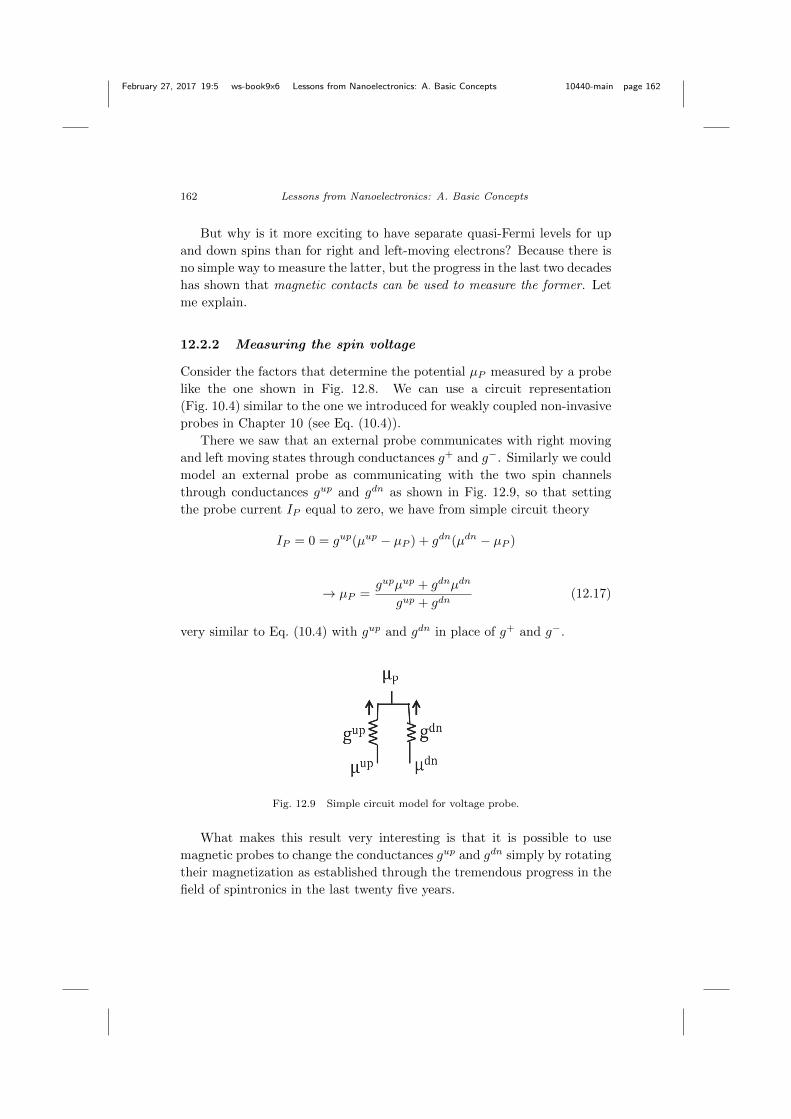
February 27, 2017 19:5 ws-book9x6 Lessons from Nanoelectronics: A. Basic Concepts 10440-main page 162
162 Lessons from Nanoelectronics: A. Basic Concepts
But why is it more exciting to have separate quasi-Fermi levels for up
and down spins than for right and left-moving electrons? Because there is
no simple way to measure the latter, but the progress in the last two decades
has shown that magnetic contacts can be used to measure the former. Let
me explain.
12.2.2 Measuring the spin voltage
Consider the factors that determine the potential µP measured by a probe
like the one shown in Fig. 12.8. We can use a circuit representation
(Fig. 10.4) similar to the one we introduced for weakly coupled non-invasive
probes in Chapter 10 (see Eq. (10.4)).
There we saw that an external probe communicates with right moving
and left moving states through conductances g+ and g−. Similarly we could
model an external probe as communicating with the two spin channels
through conductances gup and gdn as shown in Fig. 12.9, so that setting
the probe current IP equal to zero, we have from simple circuit theory
IP = 0 = gup(µup − µP ) + gdn(µdn − µP )
→ µP =gupµup + gdnµdn
gup + gdn(12.17)
very similar to Eq. (10.4) with gup and gdn in place of g+ and g−.
Fig. 12.9 Simple circuit model for voltage probe.
What makes this result very interesting is that it is possible to use
magnetic probes to change the conductances gup and gdn simply by rotating
their magnetization as established through the tremendous progress in the
field of spintronics in the last twenty five years.
February 27, 2017 19:5 ws-book9x6 Lessons from Nanoelectronics: A. Basic Concepts 10440-main page 163
Smart Contacts 163
Defining the average potential µ and the spin potential µS as
µ =µup + µdn
2(12.18a)
µS =µup − µdn
2(12.18b)
we can rewrite Eq. (12.17) with a little algebra as
µP = µ+ PµS2
(12.19a)
P ≡ gup − gdn
gup + gdn(12.19b)
where P denotes the probe polarization. A non-magnetic probe has equal
conductances gup and gdn for both spins making the polarization P equal
to zero. But magnets have unequal density of states at the Fermi energy
for up and down spins resulting in unequal conductances gup and gdn and
hence a non-zero P which could be positive or negative depending on the
magnet.
If we reverse the magnetization of the magnet, the sign of P will reverse
(either negative to positive, or positive to negative) since the role of up and
down are reversed. Using this fact we can write from Eq. (12.19)
µP (+m)− µP (−m) = 2PµS (12.20)
which affords a straightforward approach for measuring the spin potential
µS , simply by looking at the change in the probe potential on reversing its
magnetization.
12.2.3 Spin-momentum locking
Let us now get back to our earlier discussion about a special class of ma-
terials called topological insulators in which the QFL’s for right- and left-
moving states translate into those for up and down states which can then
be measured with a magnetic probe as we just discussed. However, this
translation from µ+ and µ− to µup and µdn occurs more generally in a
large class of materials with strong “spin-orbit (SO) coupling” (we will dis-
cuss this more in Part B) which exhibit surface states that have unequal
numbers M and N of up-spin and down spin modes propagating to the
right (Fig. 12.10).

February 27, 2017 19:5 ws-book9x6 Lessons from Nanoelectronics: A. Basic Concepts 10440-main page 164
164 Lessons from Nanoelectronics: A. Basic Concepts
Fig. 12.10 Surface states in materials with high spin-orbit coupling have equal number
of modes M for right moving upspins and leftmoving downspins, but a different numberof modes N for left moving upspins and right moving downspins.
Note that the situation depicted in Fig. 12.10 is different from ordinary
materials as well as from magnetic materials. Ordinarily the number of
modes is the same for left-moving and right-moving states for both up and
down spins:
M(up+) = M(dn+) = M(up−) = M(dn−) = M.
Magnetic materials on the other hand have different numbers of modes for
upspins and downspins:
M(up+) = M(up−) = M ; M(dn+) = M(dn−) = N.
What we are discussing here is different (Fig. 12.10)
M(up+) = M(dn−) = M ; M(dn+) = M(up−) = N.
This situation arises in non-magnetic materials with high spin-orbit cou-
pling which we will discuss in Part B. For the moment let us accept the
picture shown in Fig. 12.10 and note that in these materials, the up-
spin and downspin potentials µup and µdn represent different averages of
µ+ and µ−
µup =Mµ+ +Nµ−
M +Nand µdn =
Nµ+ +Mµ−
M +N(12.21)
which yields a spin potential (see Eq. (12.18))
µS =µup − µdn
2= p
µ+ − µ−
2(12.22)
where we have defined the channel polarization as
p ∼ M −NM +N
. (12.23)
February 27, 2017 19:5 ws-book9x6 Lessons from Nanoelectronics: A. Basic Concepts 10440-main page 165
Smart Contacts 165
In Eq. (12.23) we are not using the equality sign since we have glossed
over a “little” detail involving the fact that right moving electrons travel
in different directions along the surface, so that their spins also have an
angular distribution, which on averaging gives rise to a numerical factor.
Making use of Eqs. (8.8) and (4.12) we can write
I = GBµ+ − µ−
q(12.24)
we can rewrite the spin potential from Eq. (12.22) in terms of the current
I:
µS =q
2GBpI. (12.25)
Note that the channel polarization “p” appearing in Eq. (12.25) is a chan-
nel property that determines the intrinsic spin potential appearing in the
channel. It is completely different from the probe polarization “P” defined
in Eq. (12.19) which is a magnet property that comes into the picture only
when we use a magnetic probe to measure the intrinsic spin potential µSinduced in the channel by the flow of current (I).
This is a remarkable result that shows a new way of generating spin po-
tentials. The spin valves discussed in Section 12.2.1 generated spin poten-
tials through the spin-dependent interface resistance of magnetic contacts.
By contrast Eq. (12.25) tells us that a spin voltage can be generated in
channels with spin-momentum locking simply by the flow of current with-
out the need for magnetic contacts, arising from the difference between M
and N.
This is our view of the Rashba-Edelstein (RE) effect which has been
observed in a wide variety of materials like topological insulators and narrow
gap semiconductors. Similar effects are also observed in heavy metals where
it is called the spin Hall effect (SHE) and is often associated with bulk
scattering mechanisms, but there is some evidence that it could also involve
the surface mechanism described here. We will not discuss this current-
induced spin potential any further since our understanding is still evolving.
We mention it here simply because it connects spin voltages to the
notion of quasi-Fermi levels that we have been discussing in the last few
chapters and also gives the reader a feeling for the amazing progress in
spintronics that has made it possible to control and measure spin potentials.
Note that in this chapter we are using a semiclassical picture that re-
gards up and down spins simply as two types of electrons, like “red” and
“blue” electrons. This picture allows us to understand many spin-related
February 27, 2017 19:5 ws-book9x6 Lessons from Nanoelectronics: A. Basic Concepts 10440-main page 166
166 Lessons from Nanoelectronics: A. Basic Concepts
phenomena, but not all. Many phenomena involve additional subtleties
that require the quantum picture and hence can only be discussed in depth
in Part B.
12.3 Concluding Remarks
Throughout this book we have discussed how the contacts in an ordinary
device drive drainbound and sourcebound states out of equilibrium faster
than backscattering processes can restore equilibrium. The primary mes-
sage I hope to convey in this part is that QFL’s are quite real and can be
generated and measured through the use of “smart contacts”. We illustrate
this with several examples.
In p-n junctions, contacts drive the two bands out of equilibrium, faster
than R-G processes can restore equilibrium. In spin valve devices magnetic
contacts drive upspin and downspin states out of equilibrium faster than
spin-flip processes can restore equilibrium. In either case there are groups
of states A, B etc that are driven out of equilibrium by smart contacts that
can discriminate between them.
On the other hand in materials with high spin-orbit coupling, a current
injected through ordinary contacts generates a spin potential due to the
phenomenon of “spin-momentum locking” leading to unequal values of M
and N (Fig. 12.10). But to detect the spin potential we need a smart
contact. This observation is related to the Rashba-Edelstein (RE) and
perhaps the spin Hall effect (SHE) as discussed earlier.
Alternatively we could reverse the voltage and current terminals and
invoke reciprocity (Section 10.3.3) to argue that a current injected through
a smart contact will generate a voltage at the ordinary contacts. This is
related to the inverse Rashba-Edelstein (IRE) and perhaps the inverse spin
Hall effect (ISHE).
More and more of such examples can be expected in the coming years,
as we learn to control current flow not just with gate electrodes that control
the electrostatic potential, but with subtle contacting schemes that engineer
the electrochemical potential(s). Many believe that nature does just that
in designing many biological “devices”, but that is a different story.
In the context of man-made devices there are many possibilities. Per-
haps we will figure out how to contact s-orbitals differently from p-orbitals,
or one valley differently from another valley, leading to fundamentally dif-
ferent devices. But this requires a basic change in approach.

February 27, 2017 19:5 ws-book9x6 Lessons from Nanoelectronics: A. Basic Concepts 10440-main page 167
Smart Contacts 167
Traditionally, the work of device design has been divided neatly between
three groups of specialists: physicists and material scientists who innovate
new materials using atomistic theory, device engineers who worry about
contacts and related issues using macroscopic theory and circuit designers
who interconnect devices to perform useful functions.
Future devices that seek to function effectively may well require an ap-
proach that integrates materials, contacts and even circuits at the atomistic
level. Perhaps then we will be able to create devices that rival the marvels
of nature like photosynthesis.

February 27, 2017 19:5 ws-book9x6 Lessons from Nanoelectronics: A. Basic Concepts 10440-main page 168
February 27, 2017 19:5 ws-book9x6 Lessons from Nanoelectronics: A. Basic Concepts 10440-main page 169
PART 4
Heat and Electricity
169

February 27, 2017 19:5 ws-book9x6 Lessons from Nanoelectronics: A. Basic Concepts 10440-main page 170

February 27, 2017 19:5 ws-book9x6 Lessons from Nanoelectronics: A. Basic Concepts 10440-main page 171
Chapter 13
Thermoelectricity
13.1 Introduction
Conductance measurements ordinarily do not tell us anything about the
nature of the conduction process inside the conductor. If we connect the
terminals of a battery across any conductor, electron current flows out of
the negative terminal back to its positive terminal. Since this is true of all
conductors, it clearly does not tell us anything about the conductor itself.
ConventionalCurrent
Allconductors
ElectronCurrent
On the other hand, thermoelectricity, that is, electricity driven by a
temperature difference, is an example of an effect that does. A very sim-
ple experiment is to look at the current between a hot probe and a cold
probe (Fig. 13.1). For an n-type conductor (see Fig. 6.1) the direction of
the external current will be consistent with what we expect if electrons
travel from the hot to the cold probe inside the conductor, but for a p-type
conductor (see Fig. 6.2) the direction is reversed, consistent with electrons
traveling from the cold to the hot probe. Why?
It is often said that p-type conductors show the opposite effect because
the carriers have the opposite sign. As we discussed in Chapter 6, p-type
conductors involve the flow of electrons near the top of a band of ener-
171

February 27, 2017 19:5 ws-book9x6 Lessons from Nanoelectronics: A. Basic Concepts 10440-main page 172
172 Lessons from Nanoelectronics: A. Basic Concepts
gies and it is convenient to keep track of the empty states above µ rather
than the filled states below µ. These empty states are called “holes” and
since they represent the absence of an electron, they behave like positively
charged entities.
HotCold
HotCold
(a) n-typeconductor
(b) p-typeconductor
ElectronCurrent
Fig. 13.1 Thermoelectric currents driven by temperature differences flow in oppositedirections for n- and p-type conductors.
However, this is not quite satisfactory since what moves is really an
electron with a negative charge. “Holes” are at best a conceptual conve-
nience and effects observed in a laboratory should not depend on subjective
conveniences.
µ
n-type
D(E) D(E)
p-type
E
Fig. 13.2 In n-type conductors the electrochemical potential is located near the bottom
of a band of energies, while in p-type conductors it is located near the top. In n-conductors D(E) increases with increasing E, while in p-conductors it decreases with
increasing E.
February 27, 2017 19:5 ws-book9x6 Lessons from Nanoelectronics: A. Basic Concepts 10440-main page 173
Thermoelectricity 173
As we will see in this chapter the difference between n- and p-conductors
requires no new principles or assumptions beyond what we have already
discussed, namely that the current is driven by the difference between f1
and f2. The essential difference between n- and p-conductors is that while
one has a density of states D(E) that increases with energy E, the other
has a D(E) decreasing with E.
Earlier in Chapter 11 we discussed the Hall effect which too changes
sign for n-type and p-type conductors and this too is commonly blamed
on negative and positive charges. The Hall effect, however, has a totally
different origin related to the negative mass (m = p/v) associated with
E(p) relations in p-conductors that point downwards. By contrast the
thermoelectric effect does not require a conductor to even have a E(p)
relation. Even small molecules show sensible thermoelectric effects (Baheti
et al. 2008).
The basic idea is easy to see starting from our old expression for the
current obtained in Chapter 3:
I =1
q
∫ +∞
−∞dEG(E)(f1(E)− f2(E)) (same as Eq. (3.3)). (13.1)
So far the difference in f1 and f2 has been driven by difference in elec-
trochemical potentials µ1 and µ2. But it could just as well be driven by a
temperature difference, since in general
f1(E) =1
exp
(E − µ1
kT1
)+ 1
(13.2)
and
f2(E) =1
exp
(E − µ2
kT2
)+ 1
. (13.3)
But why would such a current reverse directions for an n-type and a p-type
conductor? To see this, consider two contacts with the same electrochemical
potential µ, but with different temperatures as shown in Fig. 13.3.
The key point is that the difference between f1(E) and f2(E) has a
different sign for energies E greater than µ and for energies less than µ (see
Fig. 13.3). In an n-type channel, the conductance G(E) is an increasing
function of energy, so that the net current is dominated by states with
energy E > µ and thus flows from 1 to 2, that is from hot to cold (Fig. 13.4).
But in a p-type channel it is the opposite. The conductance G(E) is a
decreasing function of energy, so that the net current is dominated by states
with energy E < µ and thus flows from 2 to 1, that is from cold to hot.

February 27, 2017 19:5 ws-book9x6 Lessons from Nanoelectronics: A. Basic Concepts 10440-main page 174
174 Lessons from Nanoelectronics: A. Basic Concepts
f1 (E)
COLDHOT
E μkT
+ve
- ve
f2 (E)f1 (E) - f2 (E)
Fig. 13.3 Two contacts with the same µ, but different temperatures: f1− f2 is positive
for E > µ, and negative for E < µ.
µ
n-type
E μkT
G(E) G(E)
p-type
f1 (E) - f2 (E)
Fig. 13.4 For n-type channels, the current for E > µ dominates that for E < µ, while
for p-type channels the current for E < µ dominates that for E > µ. Consequently,electrons flow from hot to cold across an n-type channel, but from cold to hot in a
p-type channel.
13.2 Seebeck Coefficient
Related video lecture available at course website, Unit 4: L4.2.
We can use Eq. (13.1) directly to calculate currents without making any
approximations. But it is often convenient to use a Taylor series expansion
like we did earlier (Eq. (2.10)) to obtain results that are reasonably accurate

February 27, 2017 19:5 ws-book9x6 Lessons from Nanoelectronics: A. Basic Concepts 10440-main page 175
Thermoelectricity 175
µ1,T1 µ2,T2
IElectronCurrent
for low “bias”. We could write approximately from Eq. (13.1)
I = G0(V1 − V2) + GS(T1 − T2) (13.4)
where we have defined V1 and V2 as µ1/q and µ2/q. The conductance is
given by
G0 =
∫ +∞
−∞dE G(E)
(∂f0
∂µ
)
=
∫ +∞
−∞dE
(−∂f0
∂E
)G(E) (13.5)
as we have seen before in Section 2.4. The new coefficient GS that we have
introduced is given by
GS =1
q
∫ +∞
−∞dE G(E)
(∂f0
∂T
)
=
∫ +∞
−∞dE
(−∂f0
∂E
)E − µ0
qTG(E). (13.6)
This last step, relating the derivatives with respect to T and with respect
to E, requires a little algebra (see Appendix A).
Equation (13.6) expresses mathematically the basic point we just dis-
cussed. Energies E greater and less than µ0, contribute with opposite signs
to the thermoelectric coefficient, GS . It is clear that if we wanted to design
a material with the best Seebeck coefficient, S we would try to choose a
material with all its density of states on one side of µ0 since anything on the
other side contributes with an opposite sign and brings it down. We can
visualize Eq. (13.4) as shown in Fig. 13.5, where the short circuit current
is given by
ISC = GS(T1 − T2). (13.7)
Experimentally what is often measured is the open circuit voltage
V1 − V2 = VOC = −ISCG0
= −GSG0
(T1 − T2). (13.8)

February 27, 2017 19:5 ws-book9x6 Lessons from Nanoelectronics: A. Basic Concepts 10440-main page 176
176 Lessons from Nanoelectronics: A. Basic Concepts
Note that we are using I and V for electron current and electron voltage
µ/q whose sign is opposite that of the conventional current and voltage. For
n-type conductors, for example, GS is positive, so that Eq. (13.8) tells us
that VOC is negative if T1 > T2. This means that the contact with the
higher temperature has a negative electron voltage (see Section 3.2.2 where
our convention is explained) and hence a positive conventional voltage. By
convention this is defined as a negative Seebeck coefficient.
S ≡ VOCT1 − T2
= −GSG0
(13.9)
Isc
V1 V2I
G
V1 V2I
1/G
Voc+-
00
Fig. 13.5 Circuit representations of Eq. (13.4).
13.3 Thermoelectric Figures of Merit
The practical importance of thermoelectric effects arise from the possibility
of converting waste heat into electricity and from this point of view the
important figure of merit is the amount of power that could be generated
from a given T1 − T2. What load resistor RL will maximize the power
delivered to it (Fig. 13.6)? A standard theorem in circuit theory says (this
is not too hard to prove for yourself) that the answer is a “matched load”
for which RL equal to 1/G0:
Pmax =VOC
2G0
4= S2G0
(T1 − T2)2
4. (13.10)
The quantity S2G0 is known as the power factor and is one of the
standard figures of merit for thermoelectric materials.
However, there is a second figure of merit that is more commonly used.
To see where this comes from, we first note that when the contacts are
at different temperatures, we expect a constant flow of heat through the
conductor due to its heat conductance GK
GK(T1 − T2)
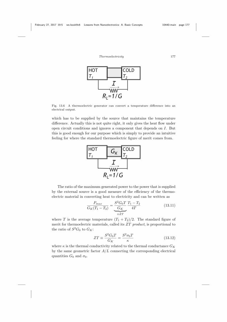
February 27, 2017 19:5 ws-book9x6 Lessons from Nanoelectronics: A. Basic Concepts 10440-main page 177
Thermoelectricity 177
HOTT1
COLDT2
I
RL=1/GFig. 13.6 A thermoelectric generator can convert a temperature difference into an
electrical output.
which has to be supplied by the source that maintains the temperature
difference. Actually this is not quite right, it only gives the heat flow under
open circuit conditions and ignores a component that depends on I. But
this is good enough for our purpose which is simply to provide an intuitive
feeling for where the standard thermoelectric figure of merit comes from.
HOTT1
COLDT2
I
RL=1/G
GK
The ratio of the maximum generated power to the power that is supplied
by the external source is a good measure of the efficiency of the thermo-
electric material in converting heat to electricity and can be written as
PmaxGK(T1 − T2)
=S2G0T
GK︸ ︷︷ ︸≡ZT
T1 − T2
4T(13.11)
where T is the average temperature (T1 + T2)/2. The standard figure of
merit for thermoelectric materials, called its ZT product, is proportional to
the ratio of S2G0 to GK :
ZT ≡ S2G0T
GK=S2σ0T
κ(13.12)
where κ is the thermal conductivity related to the thermal conductance GKby the same geometric factor A/L connecting the corresponding electrical
quantities G0 and σ0.

February 27, 2017 19:5 ws-book9x6 Lessons from Nanoelectronics: A. Basic Concepts 10440-main page 178
178 Lessons from Nanoelectronics: A. Basic Concepts
Indeed the Ohm’s law for heat conduction (known as Fourier’s law) also
needs the same correction for interface resistance namely the replacement
of L with L + λ. However, while the electrical conductivity arises solely
from charged particles like electrons, the thermal conductivity also includes
a contribution from phonons which describes the vibrations of the atoms
comprising the solid lattice. Ordinarily it is the phonon component that
dominates the thermal conductivity and we will discuss it briefly in the next
chapter. For the moment let us talk about the heat carried by electrons,
something we have not discussed so far at all.
13.4 Heat Current
Related video lecture available at course website, Unit 4: L4.3.
We have discussed the thermoelectric currents in a material with any arbi-
trary conductance function G(E). The nice thing about the elastic resistor
is that channels at different energies all conduct in parallel, so that we can
think of one energy at a time and add them up at the end. Consider a
small energy range located between E and E + dE, either above or below
the electrochemical potentials µ1 and µ2 as shown in Fig. 13.7. As we dis-
cussed in the introduction, these two channels will make contributions with
opposite signs to the Seebeck effect. Now, it has long been known that the
Seebeck effect is associated with a Peltier effect. How can we understand
this connection?
Earlier in Chapter 3 we saw that for an elastic resistor the associated
Joule heat I2R is dissipated in the contacts (see Fig. 3.2). But if we consider
the n-type or p-type channels in Fig. 13.7, it is apparent that unlike Fig. 3.2,
both contacts do not get heated.
Source Drain
μ1
(a) n-type channel
μ2Source Drain
μ1
(b) p-type channel
μ2
Fig. 13.7 A one-level elastic resistor having just one level with E = ε, (a) above or(b) below the electrochemical potentials µ1,2.

February 27, 2017 19:5 ws-book9x6 Lessons from Nanoelectronics: A. Basic Concepts 10440-main page 179
Thermoelectricity 179
Figure 13.8 is essentially the same as Fig. 3.2 except that we have shown
the heat absorbed from the surroundings rather than the heat dissipated.
For n-type conductors the heat absorbed is positive at the source, negative
at the drain, indicating that the source is cooled and the drain is heated.
For p-type conductors it is exactly the opposite. This is the essence of
the Peltier effect that forms the basis for practical thermoelectric refriger-
ators. Note that the sign of the Peltier coefficient like that of the Seebeck
coefficient is related to the sign of E − µ and not the sign of q.
ChannelSource
µ1 µ2
HeatAbsorbed+ve: n-type-ve: p-type
Drain
μ1 μ2HeatAbsorbed-ve: n-type+ve: p-type
Fig. 13.8 Same as Fig. 3.2 but showing the heat absorbed (rather than dissipated)
at each contact. For n-type conductors the heat absorbed is positive at the source,negative at the drain showing that the electrons COOL the source and HEAT the drain.
For p-type conductors it is exactly the opposite.
To write the heat current carried by electrons, we can simply extend
what we wrote for the ordinary current earlier:
I =1
q
∫ +∞
−∞dEG(E)(f1(E)− f2(E)) (same as Eq. (3.3)).
Noting that an electron with energy E carrying a charge −q also extracts
an energy E−µ1 from the source and dumps an energy E−µ2 in the drain,
we can write the heat currents IQ1 and IQ2 extracted from the source and
drain respectively as
IQ1 =1
q
∫ +∞
−∞dE
E − µ1
qG(E)(f1(E)− f2(E)) (13.13)
IQ2 =1
q
∫ +∞
−∞dE
µ2 − Eq
G(E)(f1(E)− f2(E)). (13.14)
The energy extracted from the external source per unit time is given by
IE = V I =µ1 − µ2
qI. (13.15)

February 27, 2017 19:5 ws-book9x6 Lessons from Nanoelectronics: A. Basic Concepts 10440-main page 180
180 Lessons from Nanoelectronics: A. Basic Concepts
Making use of the current equation Eq. (3.3) we can rewrite IE in the form
IE =1
q
∫ +∞
−∞dE
µ1 − µ2
qG(E)(f1(E)− f2(E))
which can be combined with the equations for IQ1 and IQ2 above to show
that the sum of all three energy currents is zero
IQ1 + IQ2 + IE = 0
as we would expect due to overall energy conservation.
13.4.1 Linear response
Just as we linearized the current equation (Eq. (3.3)) to obtain an ex-
pression for the current in terms of voltage and temperature differences
(Eq. (13.4)), we can linearize the heat current equation to obtain
IQ = GP (V1 − V2) +GQ(T1 − T2) (13.16)
where GP =
∫ +∞
−∞dE
(− ∂f0
∂E
)E − µ0
qG(E) (13.17a)
GQ =
∫ +∞
−∞dE
(− ∂f0
∂E
)(E − µ0)2
q2TG(E). (13.17b)
These are the standard expressions for the thermoelectric coefficients due
to electrons which are usually obtained from the Boltzmann equation.
I should mention that the quantity GQ we have obtained is not the
thermal conductance GK that is normally used in the ZT expression cited
earlier (Eq. (13.12)). One reason is what we have stated earlier, namely
that GK also has a phonon component that we have not yet discussed. But
there is another totally different reason. The quantity GK is defined as the
heat conductance under electrical open circuit conditions (I = 0):
GK =
(∂IQ
∂(T1 − T2)
)I=0
while it can be seen from Eq. (13.16) that GQ is the heat conductance under
electrical short circuit conditions (V = 0):
GQ =
(∂IQ
∂(T1 − T2)
)V1=V2
.

February 27, 2017 19:5 ws-book9x6 Lessons from Nanoelectronics: A. Basic Concepts 10440-main page 181
Thermoelectricity 181
However, we can rewrite Eqs. (13.4) and (13.16) in a form that gives us
the open circuit coefficients (as noted in Fig. 3.3, V and I represent the
electron voltage µ/q and the electron current, which are opposite in sign to
the conventional voltage and current)
(V1 − V2) =1
G0× I +
S, Seebeck︷ ︸︸ ︷(− GSG0
)× (T1 − T2) (13.18a)
IQ =GPG0︸︷︷︸
Peltier,Π
× I −
(GQ −
GPGSG0
)︸ ︷︷ ︸
Heat Conductance, GK
× (T1 − T2). (13.18b)
We have indicated the coefficients that are normally measured experi-
mentally and are named after the experimentalists who discovered them.
Eqs. (13.4) and (13.16), on the other hand, come more naturally in the-
oretical models because of our Taylor series expansion and it is impor-
tant to be aware of the difference. Incidentally, using the expressions in
Eqs. (13.6) and (13.17), we can see that the Peltier and Seebeck coefficients
in Eq. (13.18) obey the Kelvin relation
Π = TS (13.19)
which is a special case of the fundamental Onsager relations that the linear
coefficients are required to obey (Section 10.3.4).
13.5 The Delta Function Thermoelectric
Related video lecture available at course website, Unit 4: L4.4.
μ0
Source Drain
+
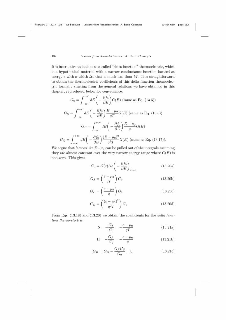
February 27, 2017 19:5 ws-book9x6 Lessons from Nanoelectronics: A. Basic Concepts 10440-main page 182
182 Lessons from Nanoelectronics: A. Basic Concepts
It is instructive to look at a so-called “delta function” thermoelectric, which
is a hypothetical material with a narrow conductance function located at
energy ε with a width ∆ε that is much less than kT . It is straightforward
to obtain the thermoelectric coefficients of this delta function thermoelec-
tric formally starting from the general relations we have obtained in this
chapter, reproduced below for convenience:
G0 =
∫ +∞
−∞dE
(− ∂f0
∂E
)G(E) (same as Eq. (13.5))
GS =
∫ +∞
−∞dE
(− ∂f0
∂E
)E − µ0
qTG(E) (same as Eq. (13.6))
GP =
∫ +∞
−∞dE
(− ∂f0
∂E
)E − µ0
qG(E)
GQ =
∫ +∞
−∞dE
(− ∂f0
∂E
)(E − µ0)2
q2TG(E) (same as Eq. (13.17)).
We argue that factors like E−µ0 can be pulled out of the integrals assuming
they are almost constant over the very narrow energy range where G(E) is
non-zero. This gives
G0 = G(ε)∆ε
(− ∂f0
∂E
)E=ε
(13.20a)
GS =
(ε− µ0
qT
)G0 (13.20b)
GP =
(ε− µ0
q
)G0 (13.20c)
GQ =
((ε− µ0)2
q2T
)G0. (13.20d)
From Eqs. (13.18) and (13.20) we obtain the coefficients for the delta func-
tion thermoelectric:
S = −GSG0
= −ε− µ0
qT(13.21a)
Π = −GPG0
= −ε− µ0
q(13.21b)
GK = GQ −GPGSG0
= 0. (13.21c)
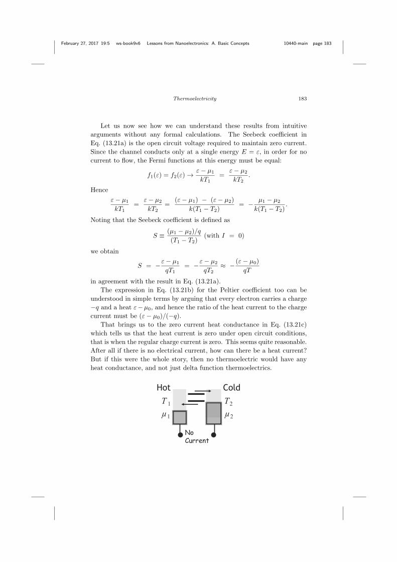
February 27, 2017 19:5 ws-book9x6 Lessons from Nanoelectronics: A. Basic Concepts 10440-main page 183
Thermoelectricity 183
Let us now see how we can understand these results from intuitive
arguments without any formal calculations. The Seebeck coefficient in
Eq. (13.21a) is the open circuit voltage required to maintain zero current.
Since the channel conducts only at a single energy E = ε, in order for no
current to flow, the Fermi functions at this energy must be equal:
f1(ε) = f2(ε)→ ε− µ1
kT1=
ε− µ2
kT2.
Hence
ε− µ1
kT1=
ε− µ2
kT2=
(ε− µ1) − (ε− µ2)
k(T1 − T2)= − µ1 − µ2
k(T1 − T2).
Noting that the Seebeck coefficient is defined as
S ≡ (µ1 − µ2)/q
(T1 − T2)(with I = 0)
we obtain
S = −ε− µ1
qT1= −ε− µ2
qT2≈ − (ε− µ0)
qT
in agreement with the result in Eq. (13.21a).
The expression in Eq. (13.21b) for the Peltier coefficient too can be
understood in simple terms by arguing that every electron carries a charge
−q and a heat ε−µ0, and hence the ratio of the heat current to the charge
current must be (ε− µ0)/(−q).That brings us to the zero current heat conductance in Eq. (13.21c)
which tells us that the heat current is zero under open circuit conditions,
that is when the regular charge current is zero. This seems quite reasonable.
After all if there is no electrical current, how can there be a heat current?
But if this were the whole story, then no thermoelectric would have any
heat conductance, and not just delta function thermoelectrics.
T 1
μ1
Hot Cold
NoCurrent
T2
μ2
February 27, 2017 19:5 ws-book9x6 Lessons from Nanoelectronics: A. Basic Concepts 10440-main page 184
184 Lessons from Nanoelectronics: A. Basic Concepts
The full story can be understood by considering a two-channel thermo-
electric with a temperature difference. Under open circuit conditions, there
is a voltage between the two contacts with µ1 < µ2. Although the total
current is zero, the individual currents in each level are non-zero. They are
equal and opposite, thereby canceling each other out. But the correspond-
ing energy currents do not cancel, since the channel with higher energy
carries more energy. Zero charge current thus does not guarantee zero heat
current, except for a delta function thermoelectric with its sharply peaked
G(E).
Since the delta function thermoelectric has zero heat conductance, the
ZT product (see Eq. (13.12)) should be very large and it would seem that
is what an ideal thermoelectric should look like. However, as we mentioned
earlier, even if the electronic heat conductance were zero, we would still
have the phonon contribution which would prevent the ZT -product from
getting too large. We will talk briefly about this aspect in the next chapter.
13.5.1 Optimizing power factor
Let us end this chapter by discussing what factors might maximize the
power factor S2G0 (see Eq. (13.10)) for a thermoelectric. If getting the
highest Seebeck coefficient S were our sole objective then it is apparent
from Eq. (13.21a) that we should choose our energy ε as far from µ0 as
possible. But that would make the conductance G0 from Eq. (13.20a)
unacceptably low, because the factor −(∂f0/∂E) dies out quickly as the
energy E moves away from µ0.
From Eqs. (13.20) and (13.21a) we have
S2G0 = G(ε)∆ε
(ε− µ0
qT
)2(− ∂f0
∂E
)E=ε
= G(ε)∆ε
kT
(k
q
)2
x2 ex
(ex + 1)2︸ ︷︷ ︸≡F (x)
, where x ≡ ε− µ0
kT. (13.22)
It is apparent from Fig. 13.9 that the function F (x) has a maximum around
x ∼ 2, suggesting that ideally we should place our level approximately
2kT above or below the electrochemical potential µ0. The corresponding

February 27, 2017 19:5 ws-book9x6 Lessons from Nanoelectronics: A. Basic Concepts 10440-main page 185
Thermoelectricity 185
F(x)
x
Fig. 13.9 Plot of F (x) ≡ x2ex
(ex+1)2.
Seebeck coefficient and power factor are approximately given by
S ≈ 2k
q(13.23a)
S2G0 ≈ 0.5
(k
q
)2
G(ε)∆ε
kT. (13.23b)
The best thermoelectrics typically have Seebeck coefficients that are not
too far from the 2(k/q) = 170 µV/K expected from Eq. (13.23a). They are
usually designed to place µ0 a little below the bottom of the band so that
the product of G(E) and −(∂f0/∂E) looks like a “delta function” around
ε a little above the bottom of the band as shown in the sketch on the left.
G(E)f0 / E
E
μ0
G(E)
E
f0 / E
μ0
The problem is that the corresponding values of conductance are not as
large as they could possibly be if µ0 were located higher up in the band as

February 27, 2017 19:5 ws-book9x6 Lessons from Nanoelectronics: A. Basic Concepts 10440-main page 186
186 Lessons from Nanoelectronics: A. Basic Concepts
sketched on the right. This would be characteristic of metals.
But metals show little promise as thermoelectric materials, because their
Seebeck coefficients are far less than k/q, since the electrochemical potential
lies in the middle of a band of states and there are nearly as many states
above µ0 as there are below µ0. For this reason the field of thermoelectric
materials is dominated by semiconductors which show the highest power
factors. However, the power factor determines only the numerator of the
ZT product in Eq. (13.12). As we mentioned earlier the heat conductance
in the denominator is dominated by phonon transport involving a physics
that is very different from the electronic transport properties that this book
is largely about. In the next chapter we will digress briefly to talk about
phonon transport.

February 27, 2017 19:5 ws-book9x6 Lessons from Nanoelectronics: A. Basic Concepts 10440-main page 187
Chapter 14
Phonon Transport
14.1 Introduction
We have seen earlier that the electrical conductivity is given by (Eq. (6.22))
σ =q2
h
(Mλ
A
)(14.1)
where the number of channels per unit area M/A and the mean free path λ
are evaluated in an energy window ∼ a few kT around µ0. The degeneracy
factor g (Section 6.4.1) due to spins and valleys is assumed to be included
in M .
In this chapter we will extend the transport theory for electrons to
handle something totally different, namely phonons and obtain a similar
expression for the thermal conductivity due to phonons
κph =π2
3
k2T
h
(Mλ
A
)ph
(14.2)
where the number of channels per unit area M/A and the mean free path λ
are evaluated in a frequency window ~ω ∼ a few kT . There is a degeneracy
factor of g = 3 due to three polarizations that is assumed to be included in
M .
Our purpose in this chapter is two-fold. The first is to provide an
interesting perspective in the hunt for high-ZT thermoelectrics. We have
seen in Chapter 13 that with careful design it is possible to achieve a Seebeck
coefficient ∼ 2k/q while maximizing the numerator in Eq. (13.12). We can
write
ZT ≈ 4k2T
q2
(σ
κ+ κph
)≈ 4
k2T
q2
σ
κph(14.3)
187
February 27, 2017 19:5 ws-book9x6 Lessons from Nanoelectronics: A. Basic Concepts 10440-main page 188
188 Lessons from Nanoelectronics: A. Basic Concepts
if we assume that the thermoelectric has been designed to provide a Seebeck
coefficient S ∼ 2k/q and the heat conductivity is dominated by phonons.
Using Eq. (14.3) with Eqs. (14.1) and (14.2) we have
ZT ≈ Mλ/A
(Mλ/A)ph(14.4)
where we have dropped a factor of 12/π2 ∼ 1 since it is just an approximate
number anyway.
This is an interesting expression suggesting that once a material has
been optimized to provide a respectable Seebeck coefficient (S), the ZT
product we obtain simply reflects the ratio of Mλ/A for electrons and
phonons. As we discussed at the end of the last chapter, the process of
achieving a high S usually puts us in a regime with a low M/A for electrons.
M/A for phonons on the other hand is often much higher ∼ 1 nm−2 at room
temperature, so that the ratio of M/A’s in Eq. (14.4) is ∼ 0.1 or less. But
electrons tend to have a longer mean free path, resulting in a ZT ∼ 1 for
the best thermoelectrics.
The most promising approach for improving ZT at this time seems
to be to try to suppress the mean free path for phonons without hurting
the electrons (the so-called “electron crystal, phonon glass”). The highest
ZT was about 1 for a long time and has recently increased to 3. Experts
say that an increase of ZT to 4 to 10 would have a major impact on its
practical applications and researchers hope that nanostructured materials
might enable this increase.
Whether they are right, only future experiments can tell, but it is clearly
of interest to understand the principles that govern ZT in nanoscale materi-
als and we hope this chapter will contribute to this understanding. But my
real objective is to demonstrate the power of the elastic resistor approach
that allows us not only to obtain linear transport coefficients for electrons
easily, but also extend the results to a totally different entity (the phonons)
with relative ease.
14.2 Phonon Heat Current
As we mentioned earlier the thermal conductance of solids has a significant
phonon component in addition to the electronic component we just talked
about. I will not go into this in any depth. My purpose is simply to show
how easily our elastic transport model is extended to something totally
different.
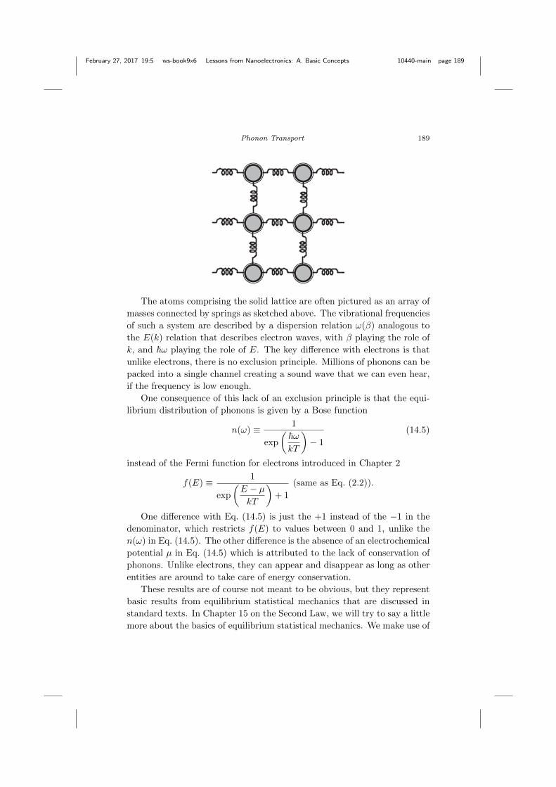
February 27, 2017 19:5 ws-book9x6 Lessons from Nanoelectronics: A. Basic Concepts 10440-main page 189
Phonon Transport 189
The atoms comprising the solid lattice are often pictured as an array of
masses connected by springs as sketched above. The vibrational frequencies
of such a system are described by a dispersion relation ω(β) analogous to
the E(k) relation that describes electron waves, with β playing the role of
k, and ~ω playing the role of E. The key difference with electrons is that
unlike electrons, there is no exclusion principle. Millions of phonons can be
packed into a single channel creating a sound wave that we can even hear,
if the frequency is low enough.
One consequence of this lack of an exclusion principle is that the equi-
librium distribution of phonons is given by a Bose function
n(ω) ≡ 1
exp
(~ωkT
)− 1
(14.5)
instead of the Fermi function for electrons introduced in Chapter 2
f(E) ≡ 1
exp
(E − µkT
)+ 1
(same as Eq. (2.2)).
One difference with Eq. (14.5) is just the +1 instead of the −1 in the
denominator, which restricts f(E) to values between 0 and 1, unlike the
n(ω) in Eq. (14.5). The other difference is the absence of an electrochemical
potential µ in Eq. (14.5) which is attributed to the lack of conservation of
phonons. Unlike electrons, they can appear and disappear as long as other
entities are around to take care of energy conservation.
These results are of course not meant to be obvious, but they represent
basic results from equilibrium statistical mechanics that are discussed in
standard texts. In Chapter 15 on the Second Law, we will try to say a little
more about the basics of equilibrium statistical mechanics. We make use of

February 27, 2017 19:5 ws-book9x6 Lessons from Nanoelectronics: A. Basic Concepts 10440-main page 190
190 Lessons from Nanoelectronics: A. Basic Concepts
these equilibrium results but we cannot really do justice to them without
a major detour from our main objective of presenting a new approach to
non-equilibrium problems.
Anyway, the bottom line is that our result for the charge current carried
by electrons
I =q
h
∫ +∞
−∞dE
(Mλ
L+ λ
)(f1(E)− f2(E)
)can be modified to represent the heat current due to phonons
IQ =1
h
∫ +∞
0
d(~ω)
(Mλ
L+ λ
)ph
~ω(n1(ω)− n2(ω)
)(14.6)
simply by making the replacements q → ~ω, E → ~ω and the Fermi func-
tions with the Bose functions:
n1(ω) ≡ 1
exp
(~ωkT1
)− 1
n2(ω) ≡ 1
exp
(~ωkT2
)− 1
and changing the lower integration limit to zero.
Again we can linearize Eq. (14.6) to write (see Appendix A)
IQ ≈ GK(T1 − T2) (14.7)
where the thermal conductance due to phonons can be written as
GK =k2T
h
∫ +∞
0
dx
(Mλ
L+ λ
)ph
x2ex
(ex − 1)2, x ≡ ~ω
kT. (14.8)
Note that just as the elastic resistor model for electrons ignores effects
due to the inelastic scattering between energy channels, this model for
phonons ignores effects due to the so-called “anharmonic interactions” that
cause phonons to convert from one frequency to another. While ballistic
electron devices have been widely studied for nearly two decades, much less
is known about ballistic phonon devices.

February 27, 2017 19:5 ws-book9x6 Lessons from Nanoelectronics: A. Basic Concepts 10440-main page 191
Phonon Transport 191
14.2.1 Ballistic phonon current
Before moving on let us take a brief detour to point out that the ballistic
conductance due to phonons is well-known though in a slightly different
form, similar to the Stefan-Boltzmann law for photons. From Eq. (14.8) we
can write the ballistic heat conductance as[Gκ
]ballistic
=k2T
h
∫ +∞
0
dx Mphx2ex
(ex − 1)2. (14.9)
To evaluate this expression we need to evaluate the number of modes which
is related to the number of wavelengths that fit into the cross-section, as
we discussed for electrons (see Eq. (6.20))
Mph =πA
(wavelength)2× 3︸︷︷︸
number of
polarizations
but we have a degeneracy factor of 3 for the three allowed polarizations.
Noting that for phonons (cs: acoustic wave velocity)
wavelength =cs
ω/2π
we have Mph =3ω2A
4πc2s=
3k2T 2A
4π~2cs2x2.
From Eq. (14.9),[GK
]ballistic
=3k4T 3
8π2~3c2s
∫ +∞
0
dxx4ex
(ex − 1)2︸ ︷︷ ︸=4π4/15
=π2k4T 3
10~3c2s.
Making use of this expression we can write the ballistic heat current from
Eq. (14.7) as [IQ
]ballistic
=π2k4T 3
10~3c2s∆T.
However, the ballistic current is usually written in a different form making
use of the relation T 3∆T = ∆(T 4/4):[IQ
]ballistic
=π2k4
40~3c2s∆(T 4) =
π2k4
40~3c2s(T1
4 − T24). (14.10)
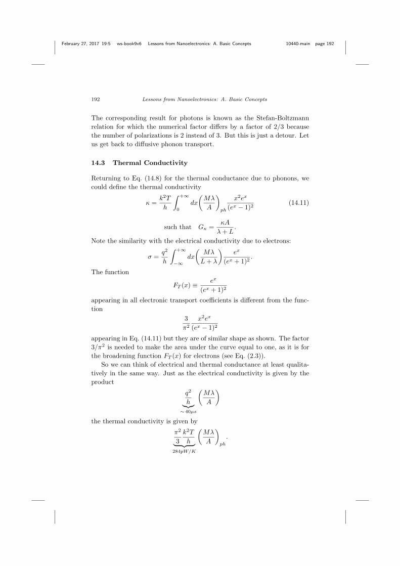
February 27, 2017 19:5 ws-book9x6 Lessons from Nanoelectronics: A. Basic Concepts 10440-main page 192
192 Lessons from Nanoelectronics: A. Basic Concepts
The corresponding result for photons is known as the Stefan-Boltzmann
relation for which the numerical factor differs by a factor of 2/3 because
the number of polarizations is 2 instead of 3. But this is just a detour. Let
us get back to diffusive phonon transport.
14.3 Thermal Conductivity
Returning to Eq. (14.8) for the thermal conductance due to phonons, we
could define the thermal conductivity
κ =k2T
h
∫ +∞
0
dx
(Mλ
A
)ph
x2ex
(ex − 1)2(14.11)
such that Gκ =κA
λ+ L.
Note the similarity with the electrical conductivity due to electrons:
σ =q2
h
∫ +∞
−∞dx
(Mλ
L+ λ
)ex
(ex + 1)2.
The function
FT (x) ≡ ex
(ex + 1)2
appearing in all electronic transport coefficients is different from the func-
tion
3
π2
x2ex
(ex − 1)2
appearing in Eq. (14.11) but they are of similar shape as shown. The factor
3/π2 is needed to make the area under the curve equal to one, as it is for
the broadening function FT (x) for electrons (see Eq. (2.3)).
So we can think of electrical and thermal conductance at least qualita-
tively in the same way. Just as the electrical conductivity is given by the
product
q2
h︸︷︷︸∼ 40µs
(Mλ
A
)
the thermal conductivity is given by
π2
3
k2T
h︸ ︷︷ ︸284pW/K
(Mλ
A
)ph
.

February 27, 2017 19:5 ws-book9x6 Lessons from Nanoelectronics: A. Basic Concepts 10440-main page 193
Phonon Transport 193
ex
(ex +1) 232
x2ex
(ex 1) 2
Fig. 14.1 Broadening function for phonons compared to that for electrons, FT (x).
These are the window functions defined by Jeong et al. (2011), see Eqs. (7e, f).
The factor π2/3 is just the inverse of the 3/π2 needed to normalize the
phonon broadening function. We mentioned at the end of the last chapter
that M/A for electrons tends to be rather small for good thermoelectric
materials whose electrochemical potential µ lies within a kT of the bottom
of the band.
One way to get around this is to use materials where the entire electronic
band of energies is a few kT wide, which is unusual. Unfortunately for the
phonon band this condition is common, giving an average M/A close to the
maximum value. The most popular thermoelectric material Bi2Te3 appears
to have a phonon bandwidth much less than kT , thus making the average
value of M/A for phonons relatively small. The phonon mean free path is
also relatively small, helping raise ZT . For example, M/A ∼ 4×10¹⁷ m−2,
λ ∼ 15 nm gives κ ∼ 2 W · m−1 · K−1, numbers that are approximately
representative of Bi2Te3.
The possible role of nanostructuring in engineering a better thermoelec-
tric is still a developing story whose ending is not clear. At this time all we
can do is to present a different viewpoint that may help us see some new
options. And that is what we have tried to do here.

February 27, 2017 19:5 ws-book9x6 Lessons from Nanoelectronics: A. Basic Concepts 10440-main page 194

February 27, 2017 19:5 ws-book9x6 Lessons from Nanoelectronics: A. Basic Concepts 10440-main page 195
Chapter 15
Second Law
15.1 Introduction
Related video lecture available at course website, Unit 4: L4.5.
Back in Chapter 13, when discussing the heat current carried by electrons
we drew a picture (Fig. 13.8) showing the flow of electrons and heat in an
elastic resistor consisting of a channel with two contacts (source and drain)
with a voltage applied across it (Fig. 15.1a). Figure 15.1b shows a slightly
generalized version of the same picture that will be useful for the present
discussion: An elastic channel receiving N1 and N2 electrons with contacts
1 and 2, held at potentials µ1 and µ2 respectively.
Of course both N1 and N2 cannot be positive. If N1 electrons enter
the channel from one contact an equal number must leave from the other
contact so that
N1 +N2 = 0. (15.1)
For generality, I have also shown an exchange of energy E0 (but not elec-
trons) with the surroundings at temperature T0, possibly by the emission
and absorption of phonons and/or photons. This exchange is absent in elas-
tic resistors. The principle of energy conservation requires that the total
energy entering the channel is zero
E1 + E2 + E0 = 0. (15.2)
This could be called an example of the first law of thermodynamics. How-
ever, there is yet another principle
E1 − µ1N1
T1+E2 − µ2N2
T2+E0
T0≤ 0 (15.3)
195
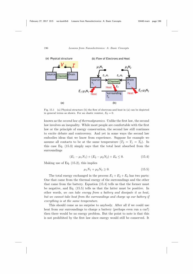
February 27, 2017 19:5 ws-book9x6 Lessons from Nanoelectronics: A. Basic Concepts 10440-main page 196
196 Lessons from Nanoelectronics: A. Basic Concepts
ChannelSource Drain
V+ - I(a) Physical structure (b) Flow of Electrons and Heat
ChannelSourceT1
DrainT2
1N1 2N2
E1,N1 E2,N2
E1- 1N1E2- 2N2
SurroundingT0
E0
Heat Heat
Heat
(a) (b)
Fig. 15.1 (a) Physical structure (b) the flow of electrons and heat in (a) can be depicted
in general terms as shown. For an elastic resistor, E0 = 0.
known as the second law of thermodynamics. Unlike the first law, the second
law involves an inequality. While most people are comfortable with the first
law or the principle of energy conservation, the second law still continues
to excite debate and controversy. And yet in some ways the second law
embodies ideas that we know from experience. Suppose for example we
assume all contacts to be at the same temperature (T2 = T1 = T0). In
this case Eq. (15.3) simply says that the total heat absorbed from the
surroundings
(E1 − µ1N1) + (E2 − µ2N2) + E0 ≤ 0. (15.4)
Making use of Eq. (15.2), this implies
µ1N1 + µ2N2 ≥ 0. (15.5)
The total energy exchanged in the process E1 +E2 +E0 has two parts:
One that came from the thermal energy of the surroundings and the other
that came from the battery. Equation (15.4) tells us that the former must
be negative, and Eq. (15.5) tells us that the latter must be positive. In
other words, we can take energy from a battery and dissipate it as heat,
but we cannot take heat from the surroundings and charge up our battery if
everything is at the same temperature.
This should come as no surprise to anybody. After all if we could use
heat from our surroundings to charge a battery (perhaps even run a car!)
then there would be no energy problem. But the point to note is that this
is not prohibited by the first law since energy would still be conserved. It

February 27, 2017 19:5 ws-book9x6 Lessons from Nanoelectronics: A. Basic Concepts 10440-main page 197
Second Law 197
is the second law that makes a distinction between the energy stored in a
battery and the thermal energy in our surroundings.
The first is easily converted into the second, but not the other way
around because thermal energy is distributed among many degrees of free-
dom. We can take energy from one degree of freedom and distribute it
among many degrees of freedom, but we cannot take energy from many
degrees of freedom and concentrate it all in one. This intuitive feeling is
quantified and generalized by the second law (Eq. (15.3)) based on solid
experimental evidence.
For example if we have multiple “contacts” at different temperatures
then as we saw in Chapter 13 it is possible to take heat from the hotter
contact, dump a part of it in the colder contact, use the difference to charge
up a battery and still be compliance with the second law. Are all the things
we have discussed so far in compliance with the second law?
The answer is yes. For the elastic resistor E0 = 0, and we can write the
second law from Eq. (15.3) in the form
ε− µ1
T1N1 +
ε− µ2
T2N2 ≤ 0
where we have written E1 = εN1 and E2 = εN2, assuming that each
electron entering and exiting the channel has an energy of ε. Making use
of Eq. (15.1) this means that(ε− µ1
T1− ε− µ2
T2
)N1 ≤ 0.
Our description of the elastic resistor always meets this condition, since the
flow of electrons is determined by f1 − f2, as we saw in Chapter 3. N1 is
positive indicating electron flow from source to drain if f1(ε) > f2(ε) that
is, if
1
1 + exp
(ε− µ1
kT
) >1
1 + exp
(ε− µ2
kT
)
ε− µ1
T1<ε− µ2
T2.
Similarly we can show that N1 is negative if
ε− µ1
T1>ε− µ2
T2.

February 27, 2017 19:5 ws-book9x6 Lessons from Nanoelectronics: A. Basic Concepts 10440-main page 198
198 Lessons from Nanoelectronics: A. Basic Concepts
In either case we have (ε− µ1
T1− ε− µ2
T2
)N1 ≤ 0
thus ensuring that the second law is satisfied. But what if we wish to go
beyond the elastic resistor and include energy exchange within the channel.
What would we need to ensure that we are complying with the second law?
15.2 Asymmetry of Absorption and Emission
T , µContact
+E,+N
-E,-N
The answer is that our model needs to ensure that for all processes involving
the exchange of electrons with a contact held at a potential µ and temper-
ature T , the probability of absorbing E, N be related to the probability of
emitting E, N by the relation
P (+E,+N)
P (−E,−N)= exp
(−E − µN
kT
). (15.6)
If only energy is exchanged, but not electrons, then the relation is modified
to
P (+E)
P (−E)= e−E/kT . (15.7)
To see how this relation (Eq. (15.6)) ensures compliance with the second
law (Eq. (15.3)), consider the process depicted in Fig. 15.1 involving energy
and/or electron exchange with three different “contacts”. Such a process
should have a likelihood proportional to
P (E1, N1)P (E2, N2)P (E0)
while the likelihood of the reverse process will be proportional to
P (−E1,−N1)P (−E2,−N2)P (−E0).
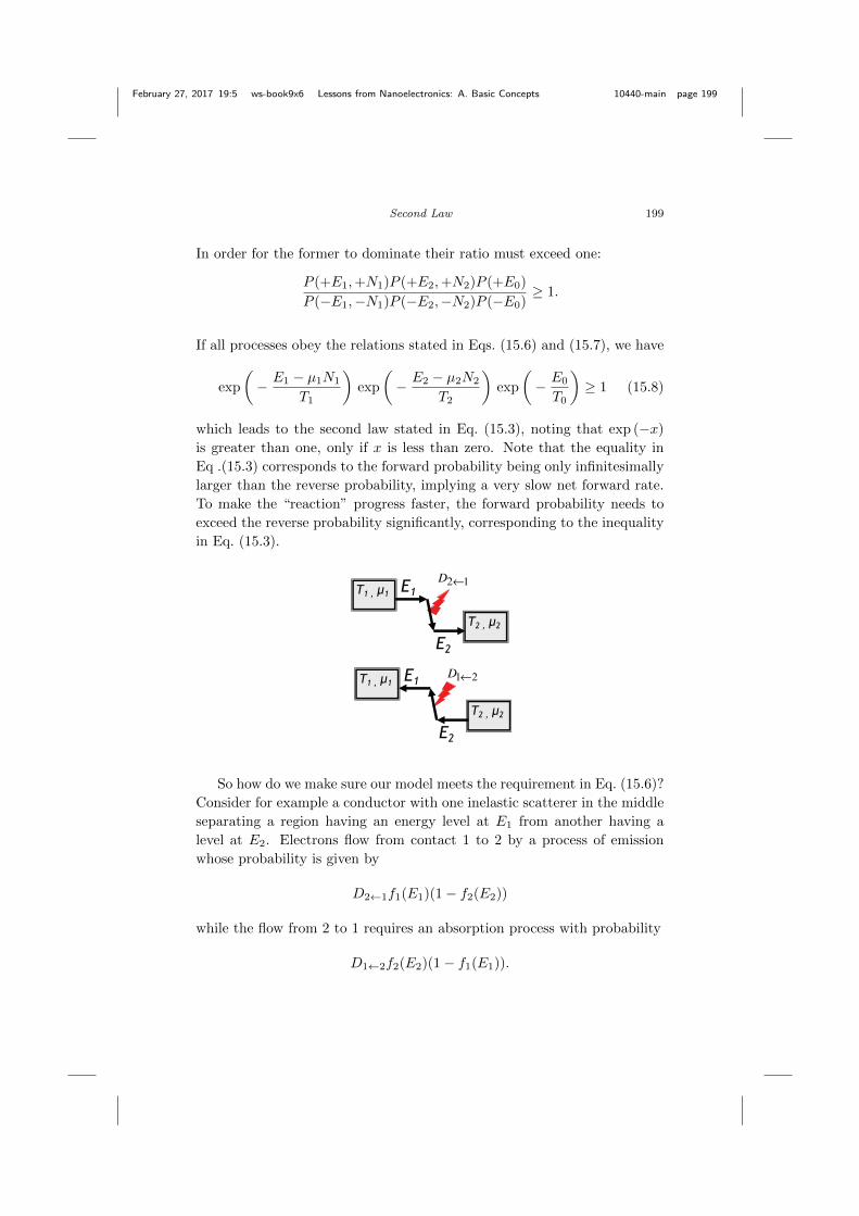
February 27, 2017 19:5 ws-book9x6 Lessons from Nanoelectronics: A. Basic Concepts 10440-main page 199
Second Law 199
In order for the former to dominate their ratio must exceed one:
P (+E1,+N1)P (+E2,+N2)P (+E0)
P (−E1,−N1)P (−E2,−N2)P (−E0)≥ 1.
If all processes obey the relations stated in Eqs. (15.6) and (15.7), we have
exp
(− E1 − µ1N1
T1
)exp
(− E2 − µ2N2
T2
)exp
(− E0
T0
)≥ 1 (15.8)
which leads to the second law stated in Eq. (15.3), noting that exp (−x)
is greater than one, only if x is less than zero. Note that the equality in
Eq .(15.3) corresponds to the forward probability being only infinitesimally
larger than the reverse probability, implying a very slow net forward rate.
To make the “reaction” progress faster, the forward probability needs to
exceed the reverse probability significantly, corresponding to the inequality
in Eq. (15.3).
E1T1 , µ1
T2 , µ2
E2
D2 1
E1T1 , µ1
T2 , µ2
E2
D1 2
So how do we make sure our model meets the requirement in Eq. (15.6)?
Consider for example a conductor with one inelastic scatterer in the middle
separating a region having an energy level at E1 from another having a
level at E2. Electrons flow from contact 1 to 2 by a process of emission
whose probability is given by
D2←1f1(E1)(1− f2(E2))
while the flow from 2 to 1 requires an absorption process with probability
D1←2f2(E2)(1− f1(E1)).

February 27, 2017 19:5 ws-book9x6 Lessons from Nanoelectronics: A. Basic Concepts 10440-main page 200
200 Lessons from Nanoelectronics: A. Basic Concepts
Since one process involves emission while the other involves absorption, the
rates should obey the requirement imposed by Eq. (15.7):
D2←1
D1←2= e(E1−E2)/kT0 (15.9)
as we had stated earlier in Chapter 12 in a different context (Eq. (12.7)).
T0 is the temperature of the surroundings with which electrons exchange
energy. The current in such an inelastic resistor would be given by an
expression of the form (suppressing the arguments E1 and E2 for clarity)
I ∼ D2←1f1(1− f2)−D1←2f2(1− f1) (15.10)
which reduces to the familiar form for elastic resistors
I ∼ (f1 − f2)
only if
D2←1 = D1←2
corresponding to elastic scattering E2 = E1.
Ordinary resistors have both elastic and inelastic scatterers intertwined
and there is no simple expression relating the current to f1 and f2. The
bottom line is that any model that includes energy exchange in the chan-
nel should make sure that absorption and emission rates are related by
Eq. (15.9) if the surroundings are in equilibrium with a fixed temperature.
Any transport theory, semiclassical or quantum needs to make sure it com-
plies with this requirement to avoid violating the second law.
15.3 Entropy
Related video lecture available at course website, Unit 4: L4.6.
The asymmetry of emission and absorption expressed by Eq. (15.6) is actu-
ally quite familiar to everyone, indeed so familiar that we may not recognize
it. We all know that if we take a hydrogen atom and place its lone electron
in an excited (say 2p) state, it will promptly emit light and descend to the
1s state. But an electron placed in the 1s state will stay there forever. We
justify it by saying that the electron “naturally” goes to its lowest energy
state. But there is really nothing natural about this. Any mechanical in-
teraction (quantum or classical) that takes an electron from 2p to 1s will
also take it from 1s to 2p.
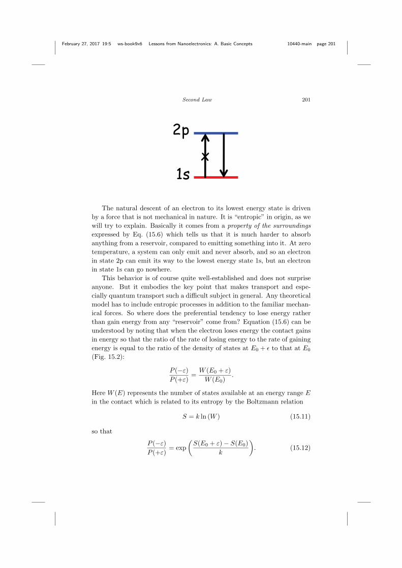
February 27, 2017 19:5 ws-book9x6 Lessons from Nanoelectronics: A. Basic Concepts 10440-main page 201
Second Law 201
1s
2px
The natural descent of an electron to its lowest energy state is driven
by a force that is not mechanical in nature. It is “entropic” in origin, as we
will try to explain. Basically it comes from a property of the surroundings
expressed by Eq. (15.6) which tells us that it is much harder to absorb
anything from a reservoir, compared to emitting something into it. At zero
temperature, a system can only emit and never absorb, and so an electron
in state 2p can emit its way to the lowest energy state 1s, but an electron
in state 1s can go nowhere.
This behavior is of course quite well-established and does not surprise
anyone. But it embodies the key point that makes transport and espe-
cially quantum transport such a difficult subject in general. Any theoretical
model has to include entropic processes in addition to the familiar mechan-
ical forces. So where does the preferential tendency to lose energy rather
than gain energy from any “reservoir” come from? Equation (15.6) can be
understood by noting that when the electron loses energy the contact gains
in energy so that the ratio of the rate of losing energy to the rate of gaining
energy is equal to the ratio of the density of states at E0 + ε to that at E0
(Fig. 15.2):
P (−ε)P (+ε)
=W (E0 + ε)
W (E0).
Here W (E) represents the number of states available at an energy range E
in the contact which is related to its entropy by the Boltzmann relation
S = k ln (W ) (15.11)
so that
P (−ε)P (+ε)
= exp
(S(E0 + ε)− S(E0)
k
). (15.12)
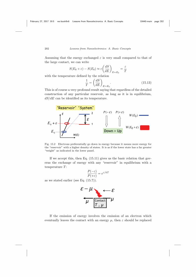
February 27, 2017 19:5 ws-book9x6 Lessons from Nanoelectronics: A. Basic Concepts 10440-main page 202
202 Lessons from Nanoelectronics: A. Basic Concepts
Assuming that the energy exchanged ε is very small compared to that of
the large contact, we can write
S(E0 + ε)− S(E0) ≈ ε(dS
dE
)E=E0
=ε
T
with the temperature defined by the relation
1
T=
(dS
dE
)E=E0
. (15.13)
This is of course a very profound result saying that regardless of the detailed
construction of any particular reservoir, as long as it is in equilibrium,
dS/dE can be identified as its temperature.
“System”“Reservoir”E
W(E)
E0 +
E0
1
2
Down > Up
P ( ) P (+ )W (E0)
W (E0 + )
Fig. 15.2 Electrons preferentially go down in energy because it means more energy for
the “reservoir” with a higher density of states. It is as if the lower state has a far greater“weight” as indicated in the lower panel.
If we accept this, then Eq. (15.11) gives us the basic relation that gov-
erns the exchange of energy with any “reservoir” in equilibrium with a
temperature T :
P (−ε)P (+ε)
= eε/kT
as we stated earlier (see Eq. (15.7)).
Contact
T , µµµ
μ
If the emission of energy involves the emission of an electron which
eventually leaves the contact with an energy µ, then ε should be replaced
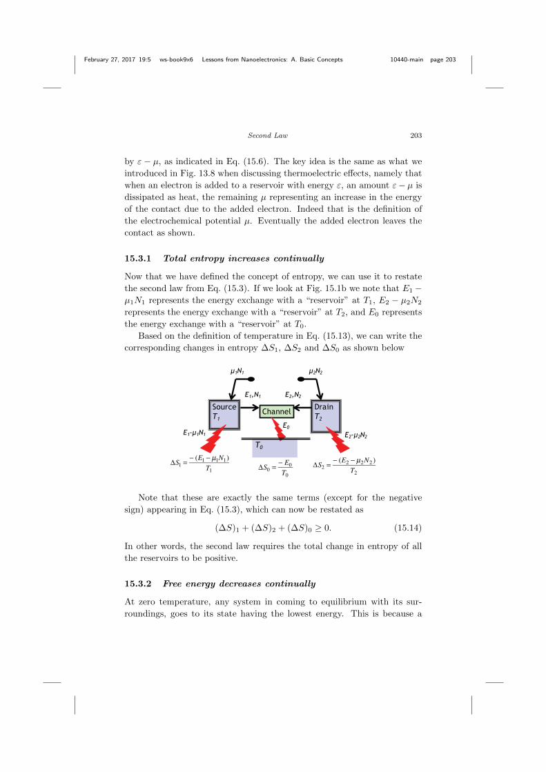
February 27, 2017 19:5 ws-book9x6 Lessons from Nanoelectronics: A. Basic Concepts 10440-main page 203
Second Law 203
by ε − µ, as indicated in Eq. (15.6). The key idea is the same as what we
introduced in Fig. 13.8 when discussing thermoelectric effects, namely that
when an electron is added to a reservoir with energy ε, an amount ε− µ is
dissipated as heat, the remaining µ representing an increase in the energy
of the contact due to the added electron. Indeed that is the definition of
the electrochemical potential µ. Eventually the added electron leaves the
contact as shown.
15.3.1 Total entropy increases continually
Now that we have defined the concept of entropy, we can use it to restate
the second law from Eq. (15.3). If we look at Fig. 15.1b we note that E1 −µ1N1 represents the energy exchange with a “reservoir” at T1, E2 − µ2N2
represents the energy exchange with a “reservoir” at T2, and E0 represents
the energy exchange with a “reservoir” at T0.
Based on the definition of temperature in Eq. (15.13), we can write the
corresponding changes in entropy ∆S1, ∆S2 and ∆S0 as shown below
ChannelSourceT1
DrainT2
µ1N1 µ2N2
E1,N1 E2,N2
E1-µ1N1 E2-µ2N2
T0
E0
S1 =(E1 μ1N1)
T1S2 =
(E2 μ2N2 )
T2S0 =
E0T0
Note that these are exactly the same terms (except for the negative
sign) appearing in Eq. (15.3), which can now be restated as
(∆S)1 + (∆S)2 + (∆S)0 ≥ 0. (15.14)
In other words, the second law requires the total change in entropy of all
the reservoirs to be positive.
15.3.2 Free energy decreases continually
At zero temperature, any system in coming to equilibrium with its sur-
roundings, goes to its state having the lowest energy. This is because a
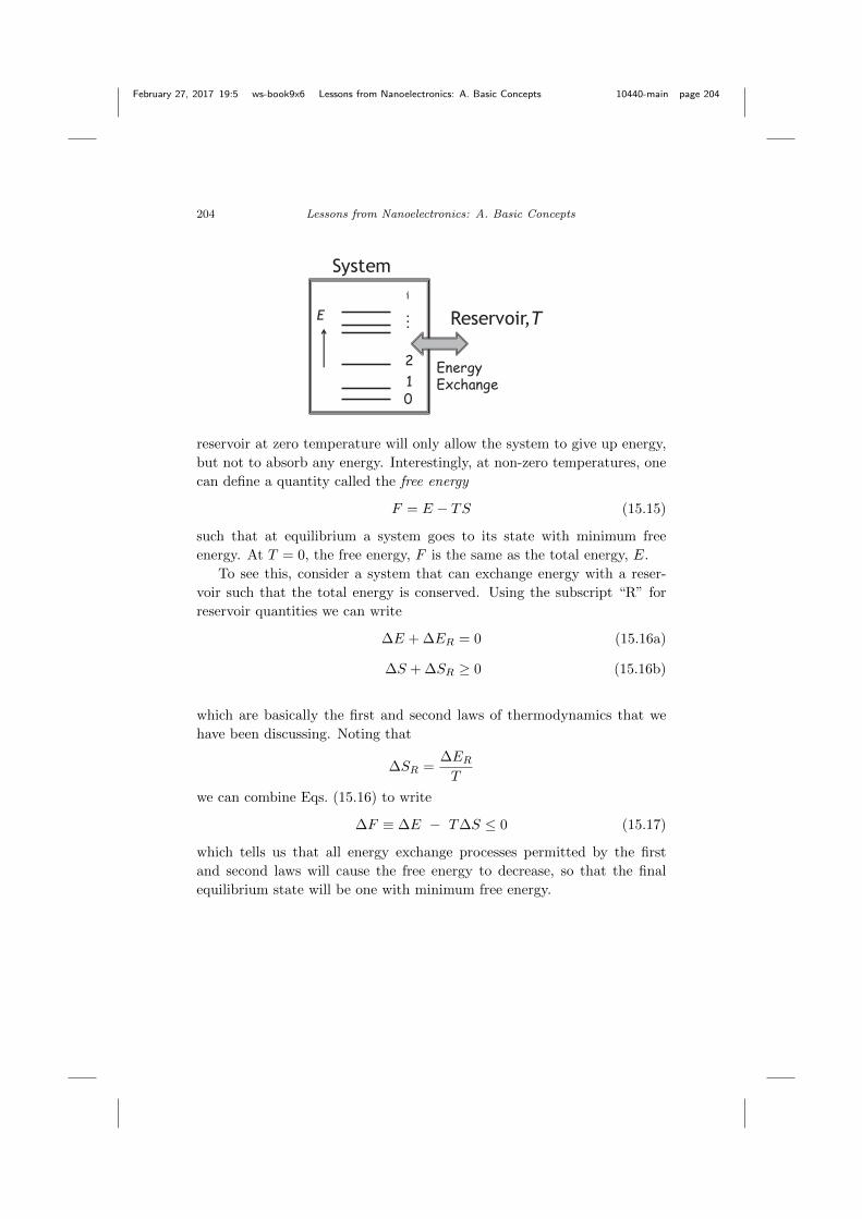
February 27, 2017 19:5 ws-book9x6 Lessons from Nanoelectronics: A. Basic Concepts 10440-main page 204
204 Lessons from Nanoelectronics: A. Basic Concepts
012
E Reservoir,T
EnergyExchange
Systemi
reservoir at zero temperature will only allow the system to give up energy,
but not to absorb any energy. Interestingly, at non-zero temperatures, one
can define a quantity called the free energy
F = E − TS (15.15)
such that at equilibrium a system goes to its state with minimum free
energy. At T = 0, the free energy, F is the same as the total energy, E.
To see this, consider a system that can exchange energy with a reser-
voir such that the total energy is conserved. Using the subscript “R” for
reservoir quantities we can write
∆E + ∆ER = 0 (15.16a)
∆S + ∆SR ≥ 0 (15.16b)
which are basically the first and second laws of thermodynamics that we
have been discussing. Noting that
∆SR =∆ERT
we can combine Eqs. (15.16) to write
∆F ≡ ∆E − T∆S ≤ 0 (15.17)
which tells us that all energy exchange processes permitted by the first
and second laws will cause the free energy to decrease, so that the final
equilibrium state will be one with minimum free energy.

February 27, 2017 19:5 ws-book9x6 Lessons from Nanoelectronics: A. Basic Concepts 10440-main page 205
Second Law 205
15.4 Law of Equilibrium
Related video lecture available at course website, Unit 4: L4.7.
The preferential tendency to lose energy rather than gain energy from any
surrounding “reservoir” as expressed in Eq. (15.6) leads to a universal law
stating that any system in equilibrium having states i with energy Ei and
with Ni particles will occupy these states with probabilities
pi =1
Ze−(Ei−µNi)/kT (15.18)
where Z is a constant chosen to ensure that all the probabilities add up to
one. To see this we note that all reservoirs in equilibrium have the property
P (+E,+N)
P (−E,−N)= exp
(−E − µN
kT
). (15.19)
“Fock space”N2
N1P(E,N )
P( E, N )
E = E1 E2 ,
N = N1 N2
E1
E2
Suppose we have a system with two states as shown exchanging energy
and electrons with the surroundings. At equilibrium, we require upward
transitions to balance downward transitions, so that
p2P (E,N) = p1P (−E,−N).
Making use of Eq. (15.6), we have
p1
p2=P (+E,+N)
P (−E,−N)= exp
(− (E1 − µN1)− (E2 − µN2)
kT
).
It is straightforward to check that the probabilities given by Eq. (15.18)
satisfy this requirement and hence represent an acceptable equilibrium so-
lution. How can we have a law of equilibrium so general that it can be
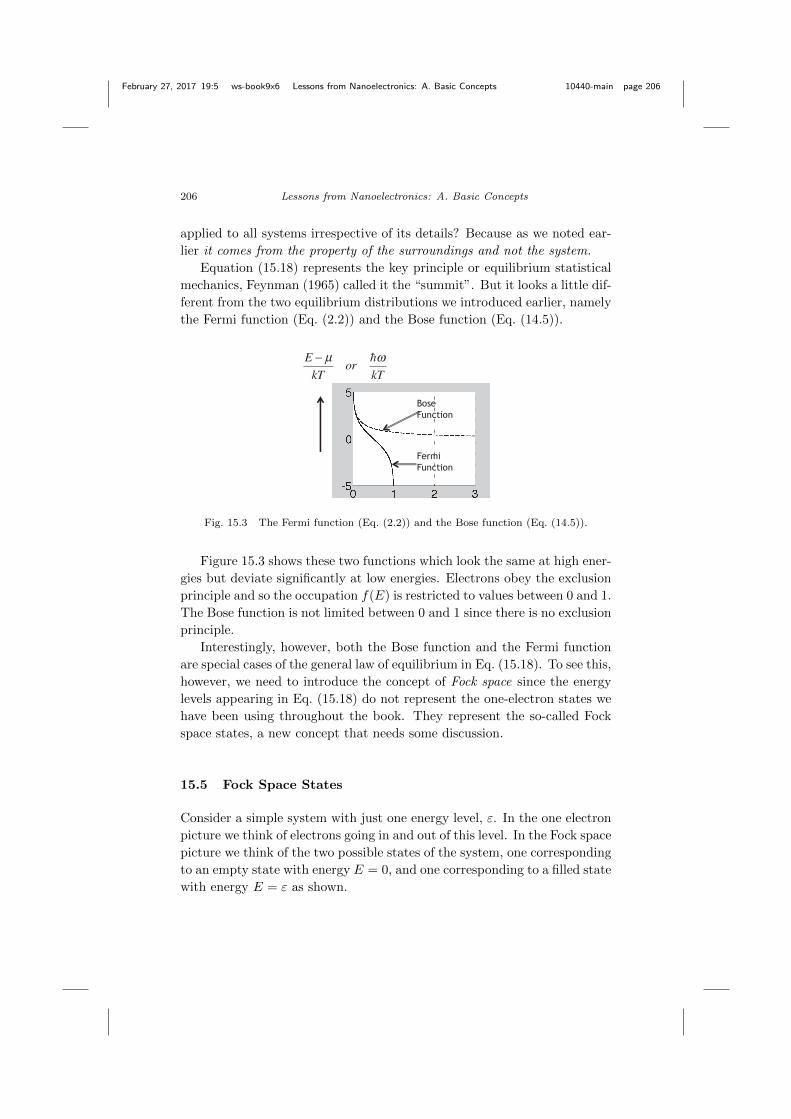
February 27, 2017 19:5 ws-book9x6 Lessons from Nanoelectronics: A. Basic Concepts 10440-main page 206
206 Lessons from Nanoelectronics: A. Basic Concepts
applied to all systems irrespective of its details? Because as we noted ear-
lier it comes from the property of the surroundings and not the system.
Equation (15.18) represents the key principle or equilibrium statistical
mechanics, Feynman (1965) called it the “summit”. But it looks a little dif-
ferent from the two equilibrium distributions we introduced earlier, namely
the Fermi function (Eq. (2.2)) and the Bose function (Eq. (14.5)).
E μ
kTor
kT
BoseFunction
FermiFunction
Fig. 15.3 The Fermi function (Eq. (2.2)) and the Bose function (Eq. (14.5)).
Figure 15.3 shows these two functions which look the same at high ener-
gies but deviate significantly at low energies. Electrons obey the exclusion
principle and so the occupation f(E) is restricted to values between 0 and 1.
The Bose function is not limited between 0 and 1 since there is no exclusion
principle.
Interestingly, however, both the Bose function and the Fermi function
are special cases of the general law of equilibrium in Eq. (15.18). To see this,
however, we need to introduce the concept of Fock space since the energy
levels appearing in Eq. (15.18) do not represent the one-electron states we
have been using throughout the book. They represent the so-called Fock
space states, a new concept that needs some discussion.
15.5 Fock Space States
Consider a simple system with just one energy level, ε. In the one electron
picture we think of electrons going in and out of this level. In the Fock space
picture we think of the two possible states of the system, one corresponding
to an empty state with energy E = 0, and one corresponding to a filled state
with energy E = ε as shown.

February 27, 2017 19:5 ws-book9x6 Lessons from Nanoelectronics: A. Basic Concepts 10440-main page 207
Second Law 207
One-electron picture
E =
“Fock space”
0
1 E =
E = 0
When an electron comes in the system goes from the empty state (0)
to the full state (1), while if an electron leaves, the system goes from 1 to
0. Applying the general law of equilibrium (Eq. (15.18)) to the Fock space
states, we have
p0 = 1/Z and p1 =e−x
Z
where x ≡ (ε− µ)/kT. (15.20)
Since the two probabilities p0 and p1 must add up to one, we have
Z = 1 + e−x
p0 =1
e−x + 1= 1− f0(ε)
p1 =e−x
e−x + 1=
1
ex + 1= f0(ε).
The probability of the system being in the full state, p1 thus equals the
Fermi function while the probability of the system being in the empty
state, p0 equals one minus the Fermi function, as we would expect.
15.5.1 Bose function
The Bose function too follows from Eq. (15.18), but we need to apply it
to a system where the number of particles go from zero to infinity. Fock
space states for electrons on the other hand are restricted to just zero or
one because of the exclusion principle.
Equation (15.18) then gives us the probability of the system being in
the N -photon state as
pN =e−Nx
Z, where x ≡ ~ω
kT.
To ensure that all probabilities add up to one, we have
Z =
∞∑N=0
e−Nx =1
1− e−x

February 27, 2017 19:5 ws-book9x6 Lessons from Nanoelectronics: A. Basic Concepts 10440-main page 208
208 Lessons from Nanoelectronics: A. Basic Concepts
“Fock space”for photons
0
1 E =
E = 0
2 E = 2
3 E = 3
so that the average number of photons is given by
n =
∞∑N=0
NpN =1
Z
∞∑N=0
Ne−Nx.
Noting that
∞∑N=0
Ne−Nx = − d
dx
∞∑N=0
e−Nx = − d
dxZ
we can show with a little algebra that
n =1
ex − 1
which is the Bose function stated earlier in Eq. (14.5).
The reason we have E−µ appearing in the Fermi function for electrons
but not ~ω−µ in the Bose function for photons or phonons is that the latter
are not conserved. As we discussed in Section 15.3, when an electron enters
the contact with energy E, it relaxes to an average energy of µ, and the
energy dissipated is E − µ. But when a photon or a phonon with energy
~ω is emitted or absorbed, the energy dissipated is just that. However,
there are conserved particles (not photons or phonons) that also obey Bose
statistics, and the corresponding Bose function has E − µ and not just E.
15.5.2 Interacting electrons
The general law of equilibrium (Eq. (15.18)) not only gives us the Fermi and
Bose functions but in principle can also describe the equilibrium state of
complicated interacting systems, if we are able to calculate the appropriate
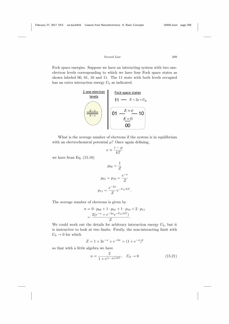
February 27, 2017 19:5 ws-book9x6 Lessons from Nanoelectronics: A. Basic Concepts 10440-main page 209
Second Law 209
Fock space energies. Suppose we have an interacting system with two one-
electron levels corresponding to which we have four Fock space states as
shown labeled 00, 01, 10 and 11. The 11 state with both levels occupied
has an extra interaction energy U0 as indicated.
What is the average number of electrons if the system is in equilibrium
with an electrochemical potential µ? Once again defining,
x ≡ ε− µkT
we have from Eq. (15.18)
p00 =1
Z
p01 = p10 =e−x
Z
p11 =e−2x
Ze−U0/kT .
The average number of electrons is given by
n = 0 · p00 + 1 · p01 + 1 · p10 + 2 · p11
=2(e−x + e−2xe−U0/kT )
Z.
We could work out the details for arbitrary interaction energy U0, but it
is instructive to look at two limits. Firstly, the non-interacting limit with
U0 → 0 for which
Z = 1 + 2e−x + e−2x = (1 + e−x)2
so that with a little algebra we have
n =2
1 + e(ε−µ)/kT, U0 → 0 (15.21)

February 27, 2017 19:5 ws-book9x6 Lessons from Nanoelectronics: A. Basic Concepts 10440-main page 210
210 Lessons from Nanoelectronics: A. Basic Concepts
equal to the Fermi function times two as we might expect since there are
two non-interacting states. The other limit is that of strongly interacting
electrons for which Z = 1 + 2e−x so that
n =1
1 +1
2e(ε−µ)/kT
, U0 →∞ (15.22)
a result that does not seem to follow in any simple way from the Fermi
function. With g one-electron states present, it takes a little more work to
show that the number is
n =1
1 +1
ge(ε−µ)/kT
, U0 →∞. (15.23)
This result may be familiar to some readers in the context of counting
electrons occupying localized states in a semiconductor.
Equilibrium statistical mechanics is a vast subject and we are of course
barely scratching the surface. My purpose here is simply to give a reader
a feel for the concept of Fock space states and how they relate to the one
electron states we have generally been talking about.
This is important because the general law of equilibrium (Eq. (15.18))
and the closely related concept of entropy (Eq. (15.11)) are both formulated
in terms of Fock space states. We have just seen how the law of equilibrium
can be translated into one-electron terms for non-interacting systems. Next
let us see how one does the same for entropy.
15.6 Alternative Expression for Entropy
Related video lecture available at course website, Unit 4: L4.8.
Equilibrium state, S = Nk n2
Consider a system of independent localized spins, like magnetic impurities
in the channel. At equilibrium, half the spins randomly point up and the
other half point down. What is the associated entropy? Equation (15.11)
defines the entropy S as k ln (W ), W being the total number of Fock space
February 27, 2017 19:5 ws-book9x6 Lessons from Nanoelectronics: A. Basic Concepts 10440-main page 211
Second Law 211
states accessible to the system. In the present problem we could argue that
each spin has two possible states (up or down) so that a collection of N
spins has a total of 2N states:
W = 2N → S = k ln (W ) = Nk ln (2). (15.24)
This is correct, but there is an alternative expression that can be used
whenever we have a system composed of a large number of identical inde-
pendent systems, like the N spin collection we are considering:
S = −Nk∑i
pi ln (pi) (15.25)
where the pi’s denote the probabilities of finding an individual system in
its ith state. An individual spin, for example has a probability of 1/2 for
being in either an up or a down state, so that from Eq. (15.25) we obtain
S = −Nk
1
2ln
(1
2
)+
1
2ln
(1
2
)= Nk ln (2)
exactly the same answer as before (Eq. (15.24)).
Equation (15.25), however, is more versatile in the sense that we can
use it easily even if the pi’s happen to be say 1/4 and 3/4 rather than 1/2
for each. Besides it is remarkably similar to the expression for the Shannon
entropy associated with the information content of a message composed of
a string of N symbols each of which can take on different values i with
probability pi. In the next chapter I will try to elaborate on this point
further.
Let me end this chapter simply by indicating how this new expression
for entropy given in Eq. (15.25) is obtained from our old one that we used
in Eq. (15.24). This is described in standard texts on statistical mechanics
(see for example, Dill and Bromberg (2003)).
15.6.1 From Eq. (15.24) to Eq. (15.25)
Consider a very large number N of identical systems each with energy levels
Ei occupied according to probabilities pi, such that the number of these
systems in state i is given by
Ni = Npi.
The total number of ways in which we can have a particular set of Ni should
equal W , so that from standard combinatorial arguments we can write
W =N !
N1!N2! . . ..
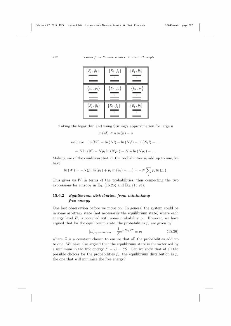
February 27, 2017 19:5 ws-book9x6 Lessons from Nanoelectronics: A. Basic Concepts 10440-main page 212
212 Lessons from Nanoelectronics: A. Basic Concepts
Ei , pi Ei , pi Ei , pi
Ei , pi Ei , pi Ei , pi
Ei , pi Ei , pi Ei , pi
Taking the logarithm and using Stirling’s approximation for large n
ln (n!) ∼= n ln (n)− n
we have ln (W ) = ln (N !)− ln (N1!)− ln (N2!)− . . .
= N ln (N)−Np1 ln (Np1)−Np2 ln (Np2)− . . .
Making use of the condition that all the probabilities pi add up to one, we
have
ln (W ) = −N(p1 ln (p1) + p2 ln (p2) + . . .) = −N∑i
pi ln (pi).
This gives us W in terms of the probabilities, thus connecting the two
expressions for entropy in Eq. (15.25) and Eq. (15.24).
15.6.2 Equilibrium distribution from minimizing
free energy
One last observation before we move on. In general the system could be
in some arbitrary state (not necessarily the equilibrium state) where each
energy level Ei is occupied with some probability pi. However, we have
argued that for the equilibrium state, the probabilities pi are given by
[pi]equilibrium =1
Ze−Ei/kT ≡ pi (15.26)
where Z is a constant chosen to ensure that all the probabilities add up
to one. We have also argued that the equilibrium state is characterized by
a minimum in the free energy F = E − TS. Can we show that of all the
possible choices for the probabilities pi, the equilibrium distribution is pithe one that will minimize the free energy?
February 27, 2017 19:5 ws-book9x6 Lessons from Nanoelectronics: A. Basic Concepts 10440-main page 213
Second Law 213
Noting that the energy of an individual system is given by
E =∑i
Eipi
and using S/N from Eq. (15.25) we can express the free energy as
F =∑i
pi(Ei + kT ln (pi)) (15.27)
which can be minimized with respect to changes in pi
dF = 0 =∑i
dpi(Ei + kT ln (pi) + kT )
=∑i
dpi(Ei + kT ln (pi))
noting that the sum of all probabilities is fixed, so that∑i
dpi = 0.
We can now argue that in order to ensure that dF is zero for arbitrary
choices of dpi we must have
Ei + kT ln (pi) = a constant
which gives us the equilibrium probabilities in Eq. (15.26).
Even if the system is not in equilibrium we can use Eq. (15.27) to
calculate the free energy F of an out-of equilibrium system if we know
the probabilities pi. But the answer should be a number larger than the
equilibrium value. In the next chapter, I will argue that in principle we can
build a device that will harness the excess free energy
∆F = F − Feq
of an out-of-equilibrium system to do useful work.
The excess free energy has two parts:
∆F︸︷︷︸excess free energy
= ∆E︸︷︷︸excess energy
− T × ∆S︸︷︷︸Information
. (15.28)
The first part represents real energy, but the second represents information
that is being traded to convert energy from the surrounding reservoirs into
work. Let us now talk abut this “fuel value of information.”

February 27, 2017 19:5 ws-book9x6 Lessons from Nanoelectronics: A. Basic Concepts 10440-main page 214
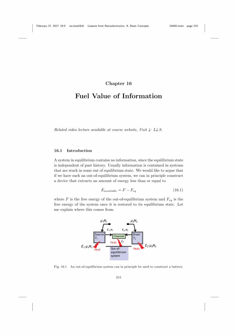
February 27, 2017 19:5 ws-book9x6 Lessons from Nanoelectronics: A. Basic Concepts 10440-main page 215
Chapter 16
Fuel Value of Information
Related video lecture available at course website, Unit 4: L4.9.
16.1 Introduction
A system in equilibrium contains no information, since the equilibrium state
is independent of past history. Usually information is contained in systems
that are stuck in some out of equilibrium state. We would like to argue that
if we have such an out-of-equilibrium system, we can in principle construct
a device that extracts an amount of energy less than or equal to
Eavailable = F − Feq (16.1)
where F is the free energy of the out-of-equilibrium system and Feq is the
free energy of the system once it is restored to its equilibrium state. Let
me explain where this comes from.
ChannelSourceT1
DrainT2
µ1N1 µ2N2
E1,N1 E2,N2
E1-µ1N1E2-µ2N2
Out-of-equilibriumsystem
E0
Heat Heat
Heat
Fig. 16.1 An out-of-equilibrium system can in principle be used to construct a battery.
215

February 27, 2017 19:5 ws-book9x6 Lessons from Nanoelectronics: A. Basic Concepts 10440-main page 216
216 Lessons from Nanoelectronics: A. Basic Concepts
Consider the general scheme discussed in the last chapter, but with both
contacts at the same temperature T and with the electrons interacting with
some metastable system. Since this system is stuck in an out-of-equilibrium
state we cannot in general talk about its temperature.
For example a collection of independent spins in equilibrium would be
randomly half up and half down at any temperature. So if we put them
into an all-up state, as shown below, we cannot talk about the temperature
of this system. But we could still use Eq. (15.25) to find its entropy, which
would be zero.
Equilibrium state, S = Nk n (2) Out - of - equilibrium state, S = 0
Fig. 16.2 A collection of N independent spins in equilibrium would be randomly half up
and half down, but could be put into an out-of-equilibrium state with all spins pointingup.
With this in mind we could rewrite the second law by replacing
E0
T0with −∆S
in Eq. (15.3):
E1 − µ1N1
T1+E2 − µ2N2
T2−∆S ≤ 0. (16.2)
Energy conservation requires that
E1 + E2 = −E0 ≡ ∆E (16.3)
where ∆E is the change in the energy of the metastable system.
Combining Eqs. (16.2) and (16.3), assuming T1 = T2 = T, and making
use of N1 +N2 = 0, we have
(µ1 − µ2)N1 ≥ ∆E − T∆S = ∆F. (16.4)
Ordinarily, ∆F can only be positive, since a system in equilibrium is at its
minimum free energy and all it can do is to increase its F . In that case,
Eq. (16.4) requires that N1 have the same sign as µ1−µ2, that is, electrons
flow from higher to lower electrochemical potential, as in any resistor.
But a system in an out-of-equilibrium state can relax to equilibrium
with a corresponding decrease in free energy, so that ∆F is negative, and N1
could have a sign opposite to that of µ1 − µ2, without violating Eq. (16.4).

February 27, 2017 19:5 ws-book9x6 Lessons from Nanoelectronics: A. Basic Concepts 10440-main page 217
Fuel Value of Information 217
μ μ
LiCoO2
μ1 μ2Li+
LixC6 Li
e- e-
C6CoO21-x
R R
Electrons could then flow from lower to higher electrochemical potential, as
they do inside a battery. The key point is that a metastable non-equilibrium
state can at least in principle be used to construct a battery.
In a way this is not too different from the way real batteries work. Take
the lithium ion battery for example. A charged battery is in a metastable
state with excess lithium ions intercalated in a carbon matrix at one elec-
trode. As lithium ions migrate out of the carbon electrode, electrons flow
in the external circuit till the battery is discharged and the electrodes have
reached the proper equilibrium state with the lowest free energy. The max-
imum energy that can be extracted is the change in the free energy. Usually
the change in the free energy F comes largely from the change in the real
energy E (recall that F = E − TS).
That does not sound too surprising. If a system starts out with an
energy E that is greater than its equilibrium energy E0, then as it relaxes,
it seems plausible that a cleverly designed device could capture the extra
energy E − E0 and deliver it as useful work. What makes it a little more
subtle, is that the extracted energy could come from the change in entropy
as well.
For example the system of localized spins shown in Fig. 16.2 in going
from the all-up state to its equilibrium state suffers no change in the actual
energy, assuming that the energy is the same whether a spin points up or
down. In this case the entire decrease in free energy comes from the increase
in entropy:
∆E = 0 (16.5a)
∆S = Nk ln (2) (16.5b)
∆F = ∆E − T∆S = −NkT ln (2). (16.5c)

February 27, 2017 19:5 ws-book9x6 Lessons from Nanoelectronics: A. Basic Concepts 10440-main page 218
218 Lessons from Nanoelectronics: A. Basic Concepts
According to Eq. (16.5) we should be able to build a device that will deliver
an amount of energy equal to NkT ln (2). In this chapter I will describe
a device based on the anti-parallel spin valve (Chapter 12) that does just
that. From a practical point of view, NkT ln (2), amounts to about 2.5 kJ
per mole, about two to three orders of magnitude lower than the available
energy of real fuels like coal or oil which comes largely from ∆E.
But the striking conceptual point is that the energy we extract is not
coming from the system of spins whose energy is unchanged. The energy
comes from the surroundings. Ordinarily the second law stops us from
taking energy from our surroundings to perform useful work. But the in-
formation contained in the non-equilibrium state in the form of “negative
entropy” allows us to extract energy from the surroundings without violat-
ing the second law.
From this point of view we could use the relation F = E − TS to split
up the right hand side of Eq. (16.1) into an actual energy and an info-
energy that can be extracted from the surroundings by making use of the
information available to us in the form of a deficit in entropy S relative to
the equilibrium value Seq:
Eavailable = E − Eeq︸ ︷︷ ︸Energy
+ T (Seq − S)︸ ︷︷ ︸Info−Energy
. (16.6)
For a set of independent localized spins in the all-up state, the available
energy is composed entirely of info-energy: there is no change in the actual
energy.
16.2 Information-driven Battery
Let us see how we could design a device to extract the info-energy from
a set of localized spins. Consider a perfect anti-parallel spin-valve device
(Chapter 12) with a ferromagnetic source that only injects and extracts
upspin electrons and a ferromagnetic drain that only injects and extracts
downspin electrons from the channel (Fig. 16.3). These itinerant electrons
interact with the localized spins through an exchange interaction of the
form
u+D ⇐⇒ U + d (16.7)
where u, d represent up and down channel electrons, while U , D represent
up and down localized spins. Ordinarily this “reaction” would be going

February 27, 2017 19:5 ws-book9x6 Lessons from Nanoelectronics: A. Basic Concepts 10440-main page 219
Fuel Value of Information 219
equally in either direction. But by starting the localized spins off in a state
with U D, we make the reaction go predominantly from right to left and
the resulting excess itinerant electrons u are extracted by one contact while
the deficiency in d electrons is compensated by electrons entering the other
contact. After some time, there are equal numbers of localized U and D
spins and the reaction goes in either direction and no further energy can
be extracted.
But what is the maximum energy that can be extracted as the localized
spins are restored from their all up state to the equilibrium state? The
answer is NkT ln (2) equal to the change in the free energy of the localized
spins as we have argued earlier.
µ1 µ2
R
Source
Drain
(a)
µ µ
RSo
urce
Drain
(b)
Fig. 16.3 An info-battery: (a) A perfect anti-parallel spin-valve device can be used toextract the excess free energy from a collection on N localized spins, all of which are
initially up. (b) Eventually the battery runs down when the spins have been randomized.
But let us see how we can get this result from a direct analysis of the
device. Assuming that the interaction is weak we expect the upspin channel
electrons (u) to be in equilibrium with contact 1 and the downspin channel
electrons (d) to be in equilibrium with contact 2, so that
fu(E) =1
exp
(E − µ1
kT
)+ 1
and fd(E) =1
exp
(E − µ2
kT
)+ 1
. (16.8)

February 27, 2017 19:5 ws-book9x6 Lessons from Nanoelectronics: A. Basic Concepts 10440-main page 220
220 Lessons from Nanoelectronics: A. Basic Concepts
Assuming that the reaction
u+D ⇐⇒ U + d
proceeds at a very slow pace so as to be nearly balanced, we can write
PD fu (1− fd) = PU fd (1− fu)
PUPD
=fu
1− fu1− fdfd
= e∆µ/kT (16.9)
where ∆µ ≡ µ1 − µ2.
Here we assumed a particular potential µ1,2 and calculated the corre-
sponding distribution of up and down localized spins. But we can reverse
this argument and view the potential as arising from a particular distribu-
tion of spins.
∆µ = kT ln
(PUPD
). (16.10)
Initially we have a larger potential difference corresponding to a pre-
ponderance of upspins (Fig. 16.3a), but eventually we end up with equal
up and down spins (Fig. 16.3b) corresponding to µ1 = µ2 = µ.
Looking at our basic reaction (Eq. (16.7)) we can see that everytime a
D flips to an U , a u flips to a d which goes out through the drain. But when
a U flips to a D, a d flips to a u which goes out through the source. So the
net number of electrons transferred from the source to the drain equals the
change in the number of U spins:
n(Source→ Drain) = −∆NU
We can write the energy extracted as the potential difference times the
number of electrons transferred
E = −∫ Final
Initial
∆µ dNU . (16.11)
Making use of Eq. (16.10) and noting that NU = N PU we can write
E = −NkT∫ Final
Initial
(ln (PU )− ln (PD)) dPU .
Noting that
dPU + dPD = 0
and that
S = −Nk(PU ln (PU ) + PD ln (PD)) (16.12)
February 27, 2017 19:5 ws-book9x6 Lessons from Nanoelectronics: A. Basic Concepts 10440-main page 221
Fuel Value of Information 221
we can use a little algebra to rewrite the integrand as
(ln (PU )− ln (PD))dPU = d(PU ln (PU ) + PD ln (PD)) = − dSNk
so that E = T
∫ Final
Initial
dS = T∆S
which is the basic result we are trying to establish, namely that the
metastable state of all upspins can in principle be used to construct a
battery that could deliver upto
T∆S = NkT ln (2)
of energy to an external load.
16.3 Fuel Value Comes from Knowledge
A key point that might bother a perceptive reader is the following. We
said that the state with all spins up has a higher free energy than that for
a random collection of spins: F > F0, and that this excess free energy can
in principle be extracted with a suitable device.
But what is it that makes the random collection different from the
ordered collection. As Feynman put it, we all feel that it is unusual to see a
car with a license plate # 9999. But it is really just as remarkable to see a
car with any specific predetermined number say 1439. Similarly if we really
knew the spins to be in a very specific but seemingly random configuration
like the one sketched here, its entropy would be zero, just like the all up
configuration. The possibility of extracting energy comes not from the all
up nature of the initial state, but from knowing exactly what state it is in.
But how would we construct our conceptual battery to extract the en-
ergy from a random but known configuration? Consider a simple configu-
ration that is not very random: the top half is up and the bottom half is
down. Ordinarily this would not give us any open circuit voltage, the top
half cancels the bottom half. But we could connect it as shown in Fig. 16.4
reversing the contacts for the left and right halves and extract energy.
Following the same principle we could construct a device to extract
energy from a more random collection too. The key point is to know the
exact configuration so that we can design the contacts accordingly.
Of course these devices would be much harder to build than the one
we started with for the all-up configuration. But these devices are just
intended to be conceptual constructs intended to illustrate a point. The
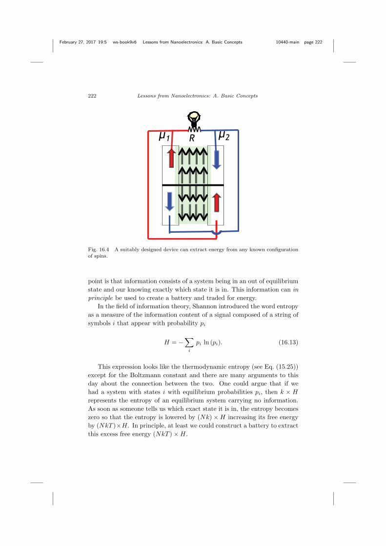
February 27, 2017 19:5 ws-book9x6 Lessons from Nanoelectronics: A. Basic Concepts 10440-main page 222
222 Lessons from Nanoelectronics: A. Basic Concepts
µ1 µ2R
Fig. 16.4 A suitably designed device can extract energy from any known configurationof spins.
point is that information consists of a system being in an out of equilibrium
state and our knowing exactly which state it is in. This information can in
principle be used to create a battery and traded for energy.
In the field of information theory, Shannon introduced the word entropy
as a measure of the information content of a signal composed of a string of
symbols i that appear with probability pi
H = −∑i
pi ln (pi). (16.13)
This expression looks like the thermodynamic entropy (see Eq. (15.25))
except for the Boltzmann constant and there are many arguments to this
day about the connection between the two. One could argue that if we
had a system with states i with equilibrium probabilities pi, then k × Hrepresents the entropy of an equilibrium system carrying no information.
As soon as someone tells us which exact state it is in, the entropy becomes
zero so that the entropy is lowered by (Nk)×H increasing its free energy
by (NkT )×H. In principle, at least we could construct a battery to extract
this excess free energy (NkT )×H.
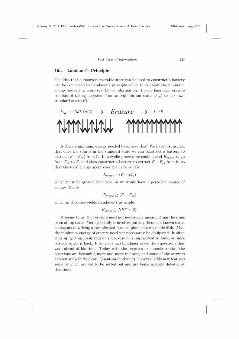
February 27, 2017 19:5 ws-book9x6 Lessons from Nanoelectronics: A. Basic Concepts 10440-main page 223
Fuel Value of Information 223
16.4 Landauer’s Principle
The idea that a known metastable state can be used to construct a battery
can be connected to Landauer’s principle which talks about the minimum
energy needed to erase one bit of information. In our language, erasure
consists of taking a system from an equilibrium state (Feq) to a known
standard state (F ):
Feq = NkT n (2) Erasure F = 0
Is there a minimum energy needed to achieve this? We have just argued
that once the spin is in the standard state we can construct a battery to
extract (F − Feq) from it. In a cyclic process we could spend Eerase to go
from Feq to F , and then construct a battery to extract F − Feq from it, so
that the total energy spent over the cycle equals
Eerase − (F − Feq)
which must be greater than zero, or we would have a perpetual source of
energy. Hence
Eerase ≥ (F − Feq)
which in this case yields Landauer’s principle:
Eerase ≥ NkT ln (2).
It seems to us, that erasure need not necessarily mean putting the spins
in an all-up state. More generally it involves putting them in a known state,
analogous to writing a complicated musical piece on a magnetic disk. Also,
the minimum energy of erasure need not necessarily be dissipated. It often
ends up getting dissipated only because it is impractical to build an info-
battery to get it back. Fifty years ago Landauer asked deep questions that
were ahead of his time. Today with the progress in nanoelectronics, the
questions are becoming more and more relevant, and some of the answers
at least seem fairly clear. Quantum mechanics, however, adds new features
some of which are yet to be sorted out and are being actively debated at
this time.

February 27, 2017 19:5 ws-book9x6 Lessons from Nanoelectronics: A. Basic Concepts 10440-main page 224
224 Lessons from Nanoelectronics: A. Basic Concepts
16.5 Maxwell’s Demon
Our info-battery could be related to Maxwell’s famous demon (see for ex-
ample, Lex (2005)) who was conjectured to beat the second law by letting
cold molecules (depicted gray) go from left to right and hot molecules (de-
picted black) go from right to left so that after some time the right hand
side becomes cold and the left hand side becomes hot (Fig. 16.5).
To see the connection with our “info-battery” in Fig. 16.3 we could draw
the following analogy:
Hot molecules ↔ up− spin electrons (u)
Cold molecules ↔ down− spin electrons (d)
Demon ↔ collection of localized spins (U, D)
Left of box ↔ source contact
Right of box ↔ drain contact.
Fig. 16.5 Maxwell’s demon creates a temperature difference by letting cold moleculesgo preferentially to the right.
Our battery is run by a set of all up localized spins that flip electrons up
and send them to the source, while replacing the down-spin from the drain.
The demon sends hot molecules to the left and cold molecules to the right,
which is not exactly the same process, but similar.
The key point, however, is that the demon is making use of informa-
tion rather than energy to create a temperature difference just as our info-
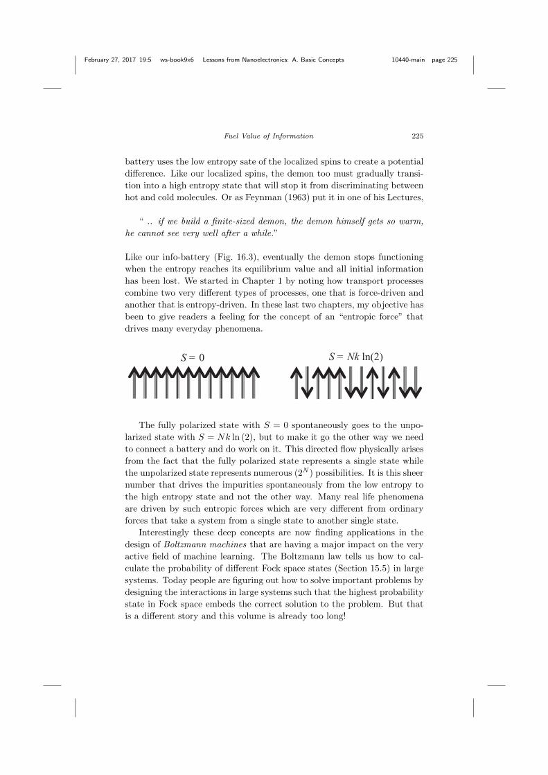
February 27, 2017 19:5 ws-book9x6 Lessons from Nanoelectronics: A. Basic Concepts 10440-main page 225
Fuel Value of Information 225
battery uses the low entropy sate of the localized spins to create a potential
difference. Like our localized spins, the demon too must gradually transi-
tion into a high entropy state that will stop it from discriminating between
hot and cold molecules. Or as Feynman (1963) put it in one of his Lectures,
“ .. if we build a finite-sized demon, the demon himself gets so warm,
he cannot see very well after a while.”
Like our info-battery (Fig. 16.3), eventually the demon stops functioning
when the entropy reaches its equilibrium value and all initial information
has been lost. We started in Chapter 1 by noting how transport processes
combine two very different types of processes, one that is force-driven and
another that is entropy-driven. In these last two chapters, my objective has
been to give readers a feeling for the concept of an “entropic force” that
drives many everyday phenomena.
S = 0 S = Nk ln(2)
The fully polarized state with S = 0 spontaneously goes to the unpo-
larized state with S = Nk ln (2), but to make it go the other way we need
to connect a battery and do work on it. This directed flow physically arises
from the fact that the fully polarized state represents a single state while
the unpolarized state represents numerous (2N ) possibilities. It is this sheer
number that drives the impurities spontaneously from the low entropy to
the high entropy state and not the other way. Many real life phenomena
are driven by such entropic forces which are very different from ordinary
forces that take a system from a single state to another single state.
Interestingly these deep concepts are now finding applications in the
design of Boltzmann machines that are having a major impact on the very
active field of machine learning. The Boltzmann law tells us how to cal-
culate the probability of different Fock space states (Section 15.5) in large
systems. Today people are figuring out how to solve important problems by
designing the interactions in large systems such that the highest probability
state in Fock space embeds the correct solution to the problem. But that
is a different story and this volume is already too long!

February 27, 2017 19:5 ws-book9x6 Lessons from Nanoelectronics: A. Basic Concepts 10440-main page 226
226 Lessons from Nanoelectronics: A. Basic Concepts
The main message I want to convey is that what makes the topic of
transport so complicated is the intertwining of force-driven and entropy-
driven phenomena. We have seen how the elastic resistor allows us to
separate the two, with entropic processes confined to the contacts, and the
channel described by semi-classical mechanics. It is time to move on to
Part B to look at the quantum version of the problem with the channel
described by quantum mechanics.

February 27, 2017 19:5 ws-book9x6 Lessons from Nanoelectronics: A. Basic Concepts 10440-main page 227
Suggested Reading
This book is based on a set of two online courses originally offered in 2012 on
nanoHUB-U and more recently in 2015 on edX. These courses are now avail-
able in self-paced format at nanoHUB-U (https://nanohub.org/u) along
with many other unique online courses.
In preparing the second edition we decided to split the book into parts A
and B following the two online courses available on nanoHUB-U entitled
Fundamentals of Nanoelectronics
Part A: Basic Concepts Part B: Quantum Transport.
Video lecture of possible interest in this context: NEGF: A Different Per-
spective.
A detailed list of video lectures available at the course website correspond-
ing to different sections of this volume (Part A: Basic Concepts) have been
listed at the beginning.
Even this Second Edition represents lecture notes in unfinished form. I plan
to keep posting additions/corrections at the book website.
This book is intended to be accessible to anyone in any branch of science
or engineering, although we have discussed advanced concepts that should
be of interest even to specialists, who are encouraged to look at my earlier
books for additional technical details.
Datta S. (1995). Electronic Transport in Mesoscopic Systems
Datta S. (2005). Quantum Transport: Atom to Transistor
227

February 27, 2017 19:5 ws-book9x6 Lessons from Nanoelectronics: A. Basic Concepts 10440-main page 228
228 Lessons from Nanoelectronics: A. Basic Concepts
Cambridge University Press
Over 50 years ago David Pines in his preface to the Frontiers in Physics
lecture note series articulated the need for both a consistent account of a
field and the presentation of a definite point of view concerning it. That
is what we have tried to provide in this book, with no intent to slight any
other point of view or perspective.
The viewpoint presented here is unique, but not the topics we discuss. Each
topic has its own associated literature that we cannot do justice to. What
follows is a very incomplete list representing a small subset of the relevant
literature, consisting largely of references that came up in the text.
Chapter 1
Figure 1.5 is reproduced from
McLennan M. et al. (1991) Voltage Drop in Mesoscopic Systems, Phys.
Rev. B, 43, 13846
A recent example of experimental measurement of potential drop across
nanoscale defects
Willke P. et al. (2015) Spatial Extent of a Landauer Residual-resistivity
Dipole in Graphene Quantified by Scanning Tunnelling Potentiom-
etry, Nature Communications, 6, 6399.
The transmission line model referenced in Section 1.8 is discussed in Sec-
tion 9.4 and is based on
Salahuddin S. et al. (2005) Transport Effects on Signal Propagation in
Quantum Wires, IEEE Trans. Electron Dev. 52, 1734
Some of the classic references on the non-equilibrium Green’s function
(NEGF) method
Martin P.C. and Schwinger J. (1959) Theory of Many-particle Systems I,
Phys. Rev. 115, 1342
Kadanoff L.P. and Baym G. (1962) Quantum Statistical Mechanics, Fron-
tiers in Physics, Lecture note series, Benjamin/Cummings
Keldysh (1965) Diagram Technique for Non-equilibrium Processes, Sov.
Phys. JETP 20, 1018

February 27, 2017 19:5 ws-book9x6 Lessons from Nanoelectronics: A. Basic Concepts 10440-main page 229
Suggested Reading 229
The quote on the importance of the “channel” concept in Section 1.8 is
taken from
Anderson P.W. (2010) 50 years of Anderson Localization, ed. E. Abra-
hams, Chapter 1, Thoughts on localization
The quote on the importance of physical pictures, even if approximate, in
Section 1.9 is taken from
Feynman R.P. (1963) Lectures on Physics, vol. II-2, Addison-Wesley.
Part I: What Determines the Resistance
Chapter 4
For an excellent physical discussion of diffusion processes and the diffusion
time (Eq. 4.7)
Berg H.C. (1993) Random Walks in Biology, Princeton University Press.
Two experiments reporting the discovery of quantized conductance in bal-
listic conductors.
van Wees, B.J. et al. (1988) Quantized Conductance of Points Contacts
in a Two-Dimensional Electron Gas, Phys. Rev. Lett. 60, 848.
Wharam, D.A. et al. (1988) One-Dimensional Transport and the Quanti-
sation of the Ballistic Resistance, J. Phys. C. 21, L209.
An experiment showing approximate conductance quantization in a hydro-
gen molecule
Smit R.H.M. et al. (2002) Measurement of the Conductance of a Hydrogen
Molecule, Nature 419, 906.
Chapter 5
For an introduction to diagrammatic methods for conductivity calculation
based on the Kubo formula, the reader could look at
Doniach S. and Sondheimer E.H. (1974), Green’s Functions for Solid
State Physicists, Frontiers in Physics Lecture Note Series, Ben-
jamin/Cummings
Also Section 5.5 of Datta (1995) cited at the beginning.
February 27, 2017 19:5 ws-book9x6 Lessons from Nanoelectronics: A. Basic Concepts 10440-main page 230
230 Lessons from Nanoelectronics: A. Basic Concepts
There is an extensive body of work on subtle correlation effects in elastic
resistors some of which have been experimentally observed. See for example,
Splettstoesser J. et al. (2010) Two-particle Aharonov-Bohm effect in Elec-
tronic Interferometers, Journal of Physics A: Mathematical and
Theoretical 43, 354027.
Part II: Simple Model for Density of States
Chapter 6
A seminal paper in the field
Thouless, D. (1977). Maximum Metallic Resistance in Thin Wires, Phys.
Rev. Lett. 39, 1167
An example of experiments showing electron density dependence of graphene
conductance
Bolotin K.I. et al. (2008) Temperature Dependent Transport in Suspended
Graphene, Phys. Rev. Lett. 101, 096802
A recent book with a thorough discussion of graphene-related materials
Torres L.E.F. Foa et al. (2014) Introduction to Graphene-based Nanoma-
terials, Cambridge University Press
Chapter 7
This discussion is based on a model pioneered by Mark Lundstrom that is
widely used in the field.
Rahman A. et al. (2003) Theory of Ballistic Transistors, IEEE Trans.
Electron Dev. 50, 1853 and references therein.
Lundstrom M.S. and Antoniadis D. (2014) Compact Models and the
Physics of Nanoscale FETs, IEEE Trans. Electron Dev. 61, 225
and references therein.
Part III: What and Where is the Voltage Drop
Section 9.4 is based on Salahuddin S. et al. (2005) cited in Chapter 1.

February 27, 2017 19:5 ws-book9x6 Lessons from Nanoelectronics: A. Basic Concepts 10440-main page 231
Suggested Reading 231
Chapter 10 is based on Chapters 2–3 of Datta (1995) cited in the beginning.
A couple of papers by the primary contributors to the subject of discussion:
Buttiker M. (1988) Symmetry of Electrical Conduction, IBM J. Res. Dev.
32, 317
Imry Y and Landauer R (1999) Conductance Viewed as Transmission, Rev.
Mod. Phys. 71, S306
To learn more about the Onsager relations the reader could look at a book
like
Yourgrau W., van der Merwe A., Raw G. (1982) Treatise on Irreversible
and Statistical Thermophysics, Dover Publications
Chapter 11
The paper that reported the first observation of the amazing quantization of
the Hall resistance:
von Klitzing K. et al. (1980) New Method for High-Accuracy Determi-
nation of the Fine Structure Constant Based on Quantized Hall
Resistance, Phys. Rev. Lett. 45, 494.
For more on edge states in the quantum Hall regime the reader could look
at Chapter 4 of Datta (1995) and references therein.
Chapter 12
An article on spin injection by one of the inventors of the spin valve
Fert A. et al. (2007) Semiconductors between Spin-Polarized Sources and
Drains, IEEE Trans. Electron Devices 54, 921
An article reviewing spin injection in semiconductors, the problems and
solutions
Schmidt G. (2005) Concepts for Spin Injection into Semiconductors a Re-
view J. Phys. D: Appl. Phys. 38, R107
To learn more about our viewpoint on electrochemical potentials in materials
with spin-momentum locking that is presented here, interested readers could
look at
February 27, 2017 19:5 ws-book9x6 Lessons from Nanoelectronics: A. Basic Concepts 10440-main page 232
232 Lessons from Nanoelectronics: A. Basic Concepts
Sayed S., Hong S. and Datta S. (2016) Multi-Terminal Spin Valve on Chan-
nels with Spin-Momentum Locking, Scientific Reports 6, 35658 and
references therein.
Part IV: Heat and Electricity
Chapter 13
On the use of the Landauer approach for thermoelectric effects
Butcher P.N. (1990) Thermal and Electrical Transport Formalism for Elec-
tronic Microstructures with Many Terminals, J. Phys. Condens.
Matt. 2, 4869 and references therein.
On the thermoelectric effects in molecules
Baheti K. et al. (2008) Probing the Chemistry of Molecular Heterojunc-
tions Using Thermoelectricity, Nano Letters 8, 715.
Paulsson M. and Datta S. (2003) Thermoelectric Effect in Molecular Elec-
tronics, Phys. Rev. B 67, 241403(R)
Chapter 14
This discussion draws on my collaborative work with Mark Lundstrom and
Changwook Jeong.
Jeong C. et al. (2011) Full dispersion versus Debye model evaluation of
lattice thermal conductivity with a Landauer approach, J. Appl.
Phys. 109, 073718-8 and references therein.
A couple of other references on the subject
Majumdar A. (1993) Microscale Heat Conduction in Dielectric Thin Films
Journal of Heat Transfer 115, 7
Mingo N. (2003) Calculation of Si nanowire thermal conductivity using
complete phonon dispersion relations, Phys. Rev. B 68, 113308
Chapter 15
To learn more about these deep concepts, the reader could look at the many
excellent texts on equilibrium statistical mechanics, such as
Dill K. and Bromberg S. (2003) Molecular Driving Forces, Statistical Ther-
modynamics in Chemistry and Biology, Garland Science
Kittel C. and Kroemer H. (1980) Thermal Physics, Freeman
February 27, 2017 19:5 ws-book9x6 Lessons from Nanoelectronics: A. Basic Concepts 10440-main page 233
Suggested Reading 233
Feynman R.P. (1965) Statistical Mechanics, Frontiers in Physics Lecture
Note Series, Benjamin/Cummings
Chapter 16
The info-battery described here follows the discussion in
Datta S. (2008) Chapter 7: Nanodevices and Maxwell’s demon in Nano
Science and Technology eds. Tang Z., Sheng P., also available at
https://arxiv.org/abs/0704.1623
See also Strasberg P. et al. (2014) Second laws for an information driven
current through a spin valve, Phys. Rev. E 90, 062107
For more on Maxwell’s demon and related issues
Feynman R.P. (1963) Lectures on Physics, vol. I-46, Addison-Wesley.
Leff H.S. and Rex A.F. (2003), Maxwell’s Demon 2, IOP Publishing.

February 27, 2017 19:5 ws-book9x6 Lessons from Nanoelectronics: A. Basic Concepts 10440-main page 234

February 27, 2017 19:5 ws-book9x6 Lessons from Nanoelectronics: A. Basic Concepts 10440-main page 235
PART 5
Appendices
235

February 27, 2017 19:5 ws-book9x6 Lessons from Nanoelectronics: A. Basic Concepts 10440-main page 236
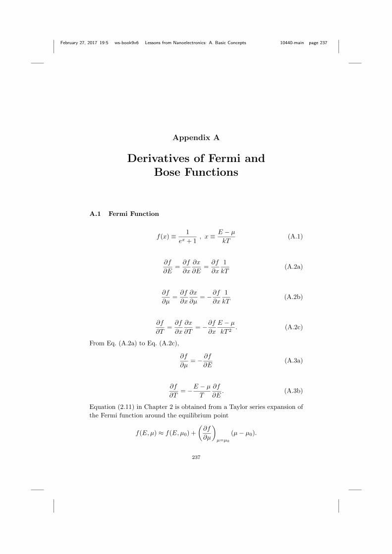
February 27, 2017 19:5 ws-book9x6 Lessons from Nanoelectronics: A. Basic Concepts 10440-main page 237
Appendix A
Derivatives of Fermi andBose Functions
A.1 Fermi Function
f(x) ≡ 1
ex + 1, x ≡ E − µ
kT(A.1)
∂f
∂E=∂f
∂x
∂x
∂E=∂f
∂x
1
kT(A.2a)
∂f
∂µ=∂f
∂x
∂x
∂µ= −∂f
∂x
1
kT(A.2b)
∂f
∂T=∂f
∂x
∂x
∂T= −∂f
∂x
E − µkT 2
. (A.2c)
From Eq. (A.2a) to Eq. (A.2c),
∂f
∂µ= − ∂f
∂E(A.3a)
∂f
∂T= −E − µ
T
∂f
∂E. (A.3b)
Equation (2.11) in Chapter 2 is obtained from a Taylor series expansion of
the Fermi function around the equilibrium point
f(E,µ) ≈ f(E,µ0) +
(∂f
∂µ
)µ=µ0
(µ− µ0).
237

February 27, 2017 19:5 ws-book9x6 Lessons from Nanoelectronics: A. Basic Concepts 10440-main page 238
238 Lessons from Nanoelectronics: A. Basic Concepts
From Eq. (A.3a), (∂f
∂µ
)µ=µ0
=
(− ∂f∂E
)µ=µ0
.
Letting f(E) stand for f(E,µ), and f0(E) stand for f(E,µ0), we can write
f(E) = f0(E) +
(− ∂f∂E
)µ=µ0
(µ− µ0)
which is the same as Eq. (2.11).
A.2 Bose Function
n(x) ≡ 1
ex − 1, x ≡ ~ω
kT(A.4)
∂n
∂T=dn
dx
∂x
∂T= − ~ω
kT 2
dn
dx
~ω∂n
∂T= −kx2 dn
dx=
kx2ex
(ex − 1)2. (A.5)
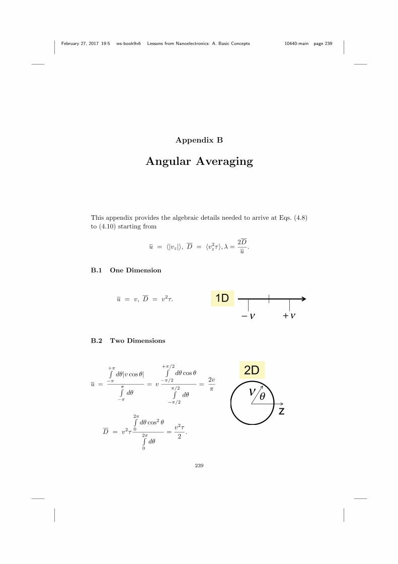
February 27, 2017 19:5 ws-book9x6 Lessons from Nanoelectronics: A. Basic Concepts 10440-main page 239
Appendix B
Angular Averaging
This appendix provides the algebraic details needed to arrive at Eqs. (4.8)
to (4.10) starting from
u = 〈|vz|〉, D = 〈v2zτ〉, λ =
2D
u.
B.1 One Dimension
u = v, D = v2τ. 1D+
B.2 Two Dimensions
u =
+π∫−π
dθ|v cos θ|
π∫−π
dθ
= v
+π/2∫−π/2
dθ cos θ
π/2∫−π/2
dθ
=2v
π
D = v2τ
2π∫0
dθ cos2 θ
2π∫0
dθ
=v2τ
2.
2D
z
239
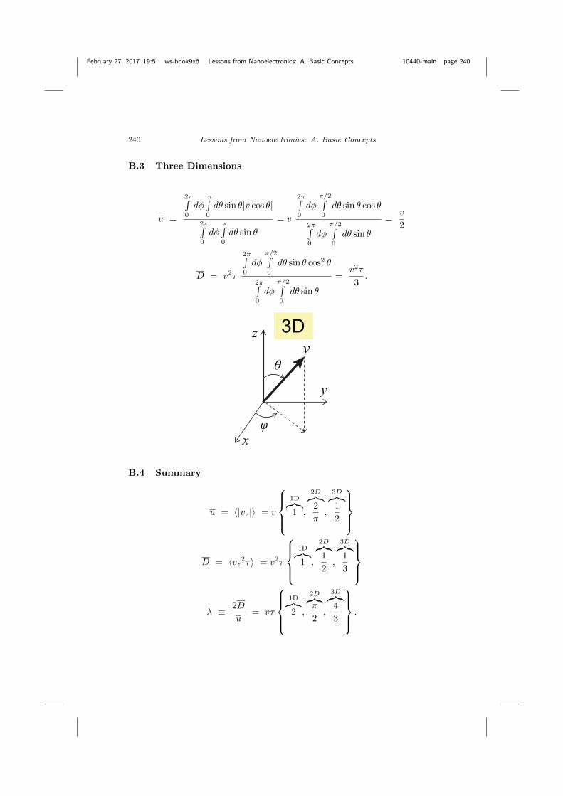
February 27, 2017 19:5 ws-book9x6 Lessons from Nanoelectronics: A. Basic Concepts 10440-main page 240
240 Lessons from Nanoelectronics: A. Basic Concepts
B.3 Three Dimensions
u =
2π∫0
dφπ∫0
dθ sin θ|v cos θ|
2π∫0
dφπ∫0
dθ sin θ
= v
2π∫0
dφπ/2∫0
dθ sin θ cos θ
2π∫0
dφπ/2∫0
dθ sin θ
=v
2
D = v2τ
2π∫0
dφπ/2∫0
dθ sin θ cos2 θ
2π∫0
dφπ/2∫0
dθ sin θ
=v2τ
3.
z
x
y
v3D
B.4 Summary
u = 〈|vz|〉 = v
1D︷︸︸︷1 ,
2D︷︸︸︷2
π,
3D︷︸︸︷1
2
D = 〈vz2τ〉 = v2τ
1D︷︸︸︷1 ,
2D︷︸︸︷1
2,
3D︷︸︸︷1
3
λ ≡ 2D
u= vτ
1D︷︸︸︷2 ,
2D︷︸︸︷π
2,
3D︷︸︸︷4
3
.
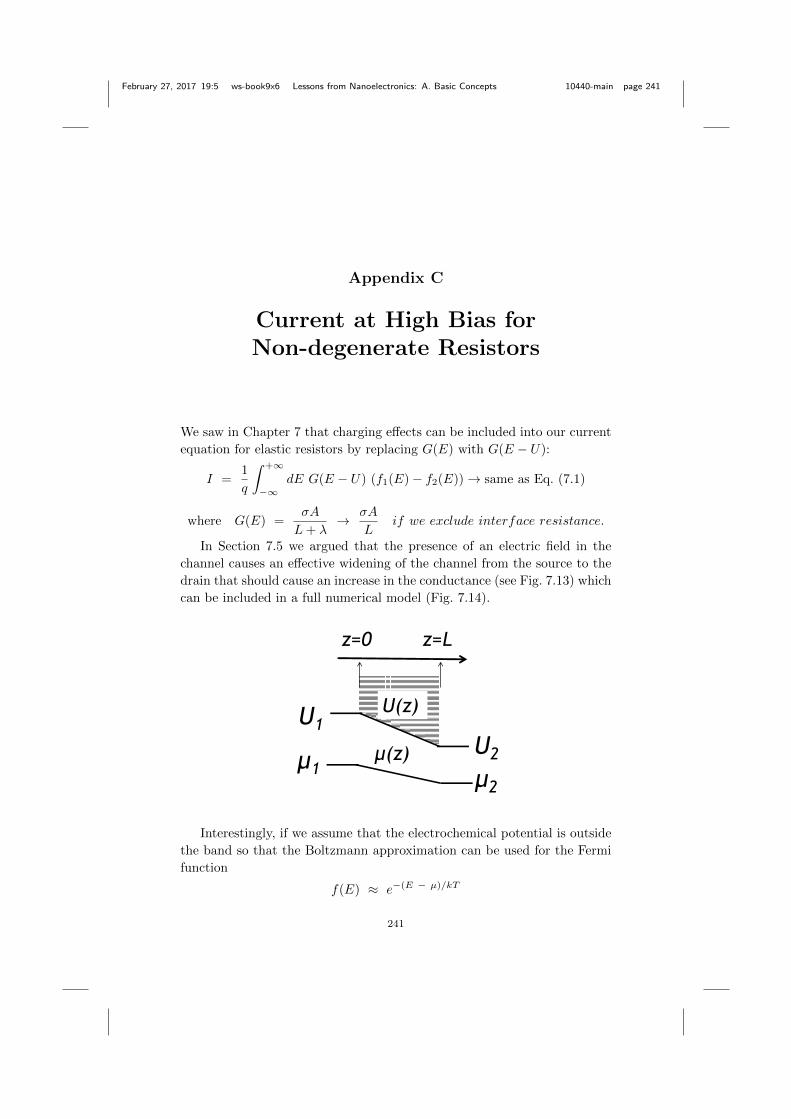
February 27, 2017 19:5 ws-book9x6 Lessons from Nanoelectronics: A. Basic Concepts 10440-main page 241
Appendix C
Current at High Bias forNon-degenerate Resistors
We saw in Chapter 7 that charging effects can be included into our current
equation for elastic resistors by replacing G(E) with G(E − U):
I =1
q
∫ +∞
−∞dE G(E − U) (f1(E)− f2(E))→ same as Eq. (7.1)
where G(E) =σA
L+ λ→ σA
Lif we exclude interface resistance.
In Section 7.5 we argued that the presence of an electric field in the
channel causes an effective widening of the channel from the source to the
drain that should cause an increase in the conductance (see Fig. 7.13) which
can be included in a full numerical model (Fig. 7.14).
U(z)
!(z)
U1U2
!2!1
z=0 z=L
Interestingly, if we assume that the electrochemical potential is outside
the band so that the Boltzmann approximation can be used for the Fermi
function
f(E) ≈ e−(E − µ)/kT
241

February 27, 2017 19:5 ws-book9x6 Lessons from Nanoelectronics: A. Basic Concepts 10440-main page 242
242 Lessons from Nanoelectronics: A. Basic Concepts
then we will show shortly that Eq. (7.1) can be used with a little modifica-
tion
I =1
q
∫ +∞
−∞dE G(E − U0) (f1(E)− f2(E)) (C.1)
G(E) =σ(E) A
l, where l ≡
∫ L
0
dz e(U(z) − U0)/kT .
Unlike the point channel model, U(z) is spatially varying and we use its
maximum value as the reference potential U0. Consequently
U(z)− U0 ≤ 0
so that l ≤ L → σA
l≥ σA
L.
This increase in conductance reflects the effective increase in the channel
width from source to drain that we discussed earlier (Fig. 7.13).
Derivation of Eq. (C.1):
This is a very nice result, but it can be derived only if we assume non-
degenerate Boltzmann statistics to express the conductivity from Eq. (6.6)
in the form
σ =
∫ +∞
−∞
dE
kTσ(E) e−E/kT︸ ︷︷ ︸σ
e(µ − U)/kT
and using it in the diffusion equation (Eq. (7.17)) to write
I
A= − σ
qe(µ−U)/kT dµ
dz
I
AeU/kT = − σkT
q
d
dzeµ/kT .
Integrating from z = 0 to z = L,
I
A
∫ L
0
dz e(U−U0)/kT︸ ︷︷ ︸l
=σ k T
qe−U0/kT (eµ1/kT − eµ2/kT )
I =1
q
A
le−U0/kT (eµ1/kT − eµ2/kT ) kT
∫ +∞
−∞
dE
kTσ(E) e−E/kT

February 27, 2017 19:5 ws-book9x6 Lessons from Nanoelectronics: A. Basic Concepts 10440-main page 243
Current at High Bias for Non-degenerate Resistors 243
=1
q
∫ +∞
−∞dE
σ(E) A
l(f1(E + U0) − f2(E + U0))
=1
q
∫ +∞
−∞dE
σ(E − U0) A
l(f1(E) − f2(E))
thus proving Eq. (C.1).
Equation (C.1) tells us that we can write the conductance of a section
of length L as being that of a section of length l that is shorter than the
physical length L. To use this result we need which requires us to know the
potential profile U(z) and this in turn would generally require a numerical
solution.
But it is interesting that for non-degenerate conductors it is possible to
write the current in a form that looks just like that for elastic resistors. For
elastic conductors, however, the Boltzmann approximation is not needed,
the current expression is valid for both degenerate and non-degenerate con-
ductors.

February 27, 2017 19:5 ws-book9x6 Lessons from Nanoelectronics: A. Basic Concepts 10440-main page 244

February 27, 2017 19:5 ws-book9x6 Lessons from Nanoelectronics: A. Basic Concepts 10440-main page 245
Appendix D
Semiclassical Dynamics
E(x,p) =(p− qA) · (p− qA)
2m+ U(x) (D.1)
where qF = −∇U , Electric Field, F
and B = ∇×A, Magnetic Field, B
D.1 Semiclassical Laws of Motion
v ≡ dx
dt= ∇pE (D.2a)
dp
dt= −∇E (D.2b)
where the gradient operators are defined as
∇E ≡ x∂E
∂x+ y
∂E
∂y+ z
∂E
∂z
∇pE ≡ x∂E
∂px+ y
∂E
∂py+ z
∂E
∂pz.
From Eqs. (D.1) and (D.2), we can show that
v = (p− qA)/m (D.3)
d(p− qA)
dt= q(F + v ×B
). (D.4)
245
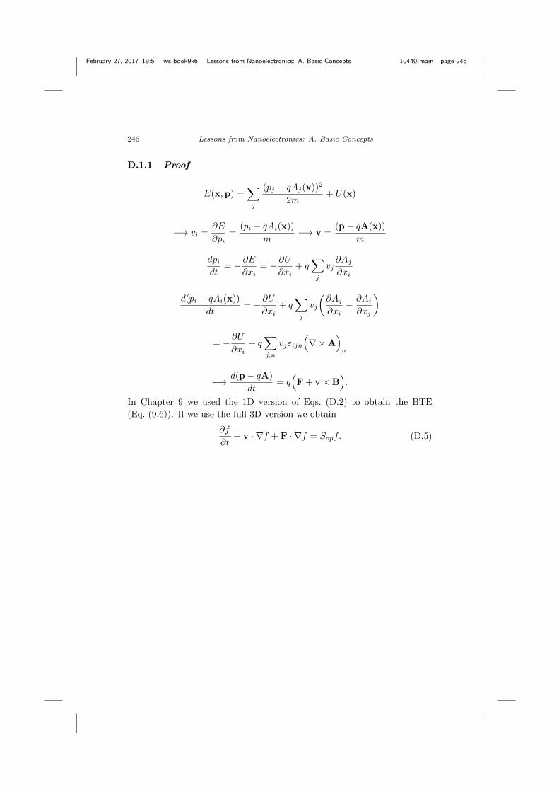
February 27, 2017 19:5 ws-book9x6 Lessons from Nanoelectronics: A. Basic Concepts 10440-main page 246
246 Lessons from Nanoelectronics: A. Basic Concepts
D.1.1 Proof
E(x,p) =∑j
(pj − qAj(x))2
2m+ U(x)
−→ vi =∂E
∂pi=
(pi − qAi(x))
m−→ v =
(p− qA(x))
m
dpidt
= − ∂E∂xi
= − ∂U∂xi
+ q∑j
vj∂Aj∂xi
d(pi − qAi(x))
dt= − ∂U
∂xi+ q
∑j
vj
(∂Aj∂xi− ∂Ai∂xj
)
= − ∂U∂xi
+ q∑j,n
vjεijn
(∇×A
)n
−→ d(p− qA)
dt= q(F + v ×B
).
In Chapter 9 we used the 1D version of Eqs. (D.2) to obtain the BTE
(Eq. (9.6)). If we use the full 3D version we obtain
∂f
∂t+ v · ∇f + F · ∇f = Sopf. (D.5)

February 27, 2017 19:5 ws-book9x6 Lessons from Nanoelectronics: A. Basic Concepts 10440-main page 247
Appendix E
Transmission Line Parameters fromBTE
In this Appendix, I will try to outline the steps involved in getting from
Eq. (9.19) to Eq. (9.20), that is
from∂µ
∂t+ vz
∂µ
∂z− ∂E
∂t= −µ− µ
τ(E.1)
to∂(µ/q)
∂z= −(LK + LM )
∂I
∂t− I
σA(E.2a)
∂(µ/q)
∂t= −
(1
CQ+
1
CE
)∂I
∂z. (E.2b)
First we separate Eq. (E.1) into two equations for µ+ and µ−,
∂µ+
∂t+ vz
∂µ+
∂z− ∂E+
∂t= −µ
+ − µτ
(E.3a)
∂µ−
∂t− vz
∂µ−∂z− ∂E−
∂t= −µ
− − µτ
. (E.3b)
Next we add and subtract Eqs. (E.3a) and (E.3b) and use the relations
I =qM
h(µ+ − µ−) and µ =
µ+ + µ−
2≡ µ
to obtain 2∂µ
∂t+
vzqM/h
∂I
∂z− ∂
∂t
(E+ + E−
)= 0
and1
qM/h
∂I
∂t+ 2vz
∂µ
∂z− ∂
∂t
(E+ + E−
)= − I
(qM/h)τ.
247
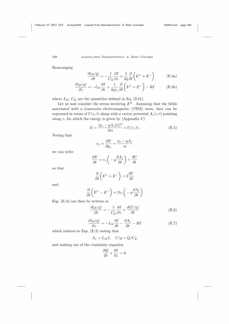
February 27, 2017 19:5 ws-book9x6 Lessons from Nanoelectronics: A. Basic Concepts 10440-main page 248
248 Lessons from Nanoelectronics: A. Basic Concepts
Rearranging
∂(µ/q)
∂t= − 1
CQ
∂I
∂z+
1
2q
∂
∂t
(E+ + E−
)(E.4a)
∂(µ/q)
∂z= −LK
∂I
∂t+
1
2qvz
∂
∂t
(E+ + E−
)−RI (E.4b)
where LK , CQ are the quantities defined in Eq. (9.21).
Let us now consider the terms involving E±. Assuming that the fields
associated with a transverse electromagnetic (TEM) wave, they can be
expressed in terms of U(z, t) along with a vector potential Az(z, t) pointing
along z, for which the energy is given by (Appendix C)
E =(pz − qAz(t))2
2m+ U(z, t). (E.5)
Noting that
vz =∂E
∂pz=pz − qAz
m
we can write
∂E
∂t= vz
(− q ∂Az
∂t
)+∂U
∂t
so that
∂
∂t
(E+ + E−
)= 2
∂U
∂t
and
∂
∂t
(E+ − E−
)= 2vz
(− q ∂Az
∂t
)Eqs. (E.4) can then be written as
∂(µ/q)
∂t= − 1
CQ
∂I
∂z+∂(U/q)
∂t(E.6)
∂(µ/q)
∂z= −LK
∂I
∂t− ∂Az
∂t−RI (E.7)
which reduces to Eqs. (E.2) noting that
Az = LMI, U/q = Q/CE
and making use of the continuity equation
∂Q
∂t+∂I
∂z= 0.
February 27, 2017 19:5 ws-book9x6 Lessons from Nanoelectronics: A. Basic Concepts 10440-main page 249
Index
Anderson localization, 17angular average of velocity, 47average
conductivity, 60velocity, 46
Buttiker formula, 124ballistic, 4
conductance, 4, 45, 48, 59, 67resistance, 6time, 46
Boltzmann approximation, 41, 84Boltzmann relation, 201Boltzmann Transport Equation, 13,
111Bose function, 30, 54, 189, 206boundary condition, 99
periodic, 68
capacitance, 118carbon nanotube, 68channel, 1charging effect, 84coherent transport, 15complementary transistor pair, 2conductance, 3, 33
function, 32quantum, 45, 48
conductivity, 3, 59, 72conductor
n-type, 70, 76, 143, 171
p-type, 70, 76, 143, 171contact, 102continuity equation, 90, 99Coulomb interaction, 36current correlation, 52current-voltage characteristics, 81,
155cyclotron frequency, 144
de Broglie principle, 65de Broglie wavelength, 49degeneracy factor, 68, 73, 159degenerate conductor, 40degenerate Einstein relation, 60degrees of freedom, 10, 197delta function thermoelectric, 181density of states (DOS), 6, 22, 63, 66,
81double-ended, 71
derivative ofFermi function, 25
diffusion coefficient, 6, 59diffusion constant, 46diffusion equation, 99diffusive, 3dispersion relation, 63
isotropic, 64linear, 64parabolic, 63, 81
drift velocity, 29drift-diffusion equation, 90
249
February 27, 2017 19:5 ws-book9x6 Lessons from Nanoelectronics: A. Basic Concepts 10440-main page 250
250 Lessons from Nanoelectronics: A. Basic Concepts
Drude formula, 5, 29, 59, 141
edge states, 135, 148effective mass, 5, 59elastic, 32elastic resistor, 10, 14, 31electric field, 8, 21electrochemical potential, 7, 10, 22,
102, 104, 121electron density, 59, 62, 69, 72electrostatic asymmetry, 87electrostatic capacitance, 86electrostatic potential, 7ensemble average, 52entropy, 13, 200entropy-driven process, 13equilibrium, 26, 80, 116exclusion principle, 25, 30, 36, 207extended channel model, 88
Fermi function, 24, 206Fermi surface, 60Feynman, 17, 225Field Effect Transistor, 1floor function, 49, 67fluctuation-dissipation theorem, 52Fock space, 206force-driven process, 13four-terminal conductance, 123four-terminal measurement, 122free electron, 30, 60free energy, 204
graphene, 60, 64group velocity, 65
Hall effect, 139Hall resistance, 141heat conductance, 176heat current, 178hole, 33, 60, 140, 172hot electron, 33
inductancekinetic, 118magnetic, 118
inelastic processes, 11, 156inelastic scattering, 38info-energy, 218interaction energy, 209interface resistance, 6, 38, 45, 91, 101inverter, 2
Joule heat, 11, 32
Kelvin relation, 181Kubo formula, 52, 136
Landauer formula, 124Landauer resistor, 11Landauer’s principle, 223law of equilibrium, 205linear response, 27low bias conductance, 32, 52low temperature approximation, 82
magnetic force, 139magnetic tunnel junction, 160magnetoresistance, 160Maxwell’s demon, 224mean free path, 3, 59mean free time, 59
for back scattering, 47mobility, 59momentum relaxation time, 5, 29Moore’s Law, 4
nanotransistor, 75negative entropy, 218NEGF formalism, 14Newton’s Law, 13, 29non-degenerate conductor, 29, 40non-reciprocal circuits, 135number of modes, 5, 17, 45, 49, 67, 82number of states, 62
occupation factor, 106, 111Ohm’s Law, 3, 44one-level resistor, 54Onsager relations, 136orthogonal states, 37out-of-equilibrium, 102

February 27, 2017 19:5 ws-book9x6 Lessons from Nanoelectronics: A. Basic Concepts 10440-main page 251
Index 251
p-n junction, 12, 21, 153Peltier coefficient, 179Peltier effect, 12, 178phonon, 30, 187phonon broadening function, 193Planck’s constant, 65point channel model, 22, 76, 88Poisson equation, 92polarization, 160power factor, 176
quantum capacitance, 83, 85, 118quantum Hall effect, 148quantum transport, 13quasi-Fermi level, 8, 107, 152
Rashba-Edelstein effect, 165rectifier, 86relaxation time approximation, 113resistance, 1resistivity, 3
saturation current, 78, 83scattering operator, 113Schrodinger equation, 13Seebeck coefficient, 174self-consistent procedure, 81Shannon entropy, 211, 222Sharvin resistance, 48, 124
single band relation, 61, 142single electron charging energy, 86skipping orbits, 148spin Hall effect, 165spin potential, 159spin valve, 159spin-momentum locking, 163spin-orbit coupling, 161spintronics, 18Stefan-Boltzmann relation, 192Stirling’s approximation, 212sum rules, 130
Taylor series, 28thermal broadening function, 25, 60thermal conductivity, 177, 192
due to phonons, 187thermodynamics
first law, 195second law, 196
thermoelectricity, 171topological insulators, 161transit time, 43transmission line, 17transmission probability, 122
valley, 73
ZT-product, 177