Lesson #5 Chapter 2 - New Jersey Institute of Technologyjoelsd/electronics/classwork/...BME 372...
42
BME 372 Electronics I – J.Schesser 138 Operational Amplifiers Lesson #5 Chapter 2
Transcript of Lesson #5 Chapter 2 - New Jersey Institute of Technologyjoelsd/electronics/classwork/...BME 372...
BME 372 Electronics I –J.Schesser
138
Operational Amplifiers
Lesson #5Chapter 2

BME 372 Electronics I –J.Schesser
139
Operational Amplifiers
• An operational Amplifier is an ideal differential with the following characteristics:– Infinite input impedance– Infinite gain for the differential signal– Zero gain for the common-mode signal– Zero output impedance– Infinite Bandwidth vo-
+
v1
v2
Inverting input
Non-Inverting input

BME 372 Electronics I –J.Schesser
140
Operational Amplifier Feedback• Operational Amplifiers are used with negative feedback• Feedback is a way to return a portion of the output of an
amplifier to the input– Negative Feedback: returned output opposes the source signal– Positive Feedback: returned output aids the source signal
• For Negative Feedback– In an Op-amp, the negative feedback returns a fraction of the
output to the inverting input terminal forcing the differential input to zero.
– Since the Op-amp is ideal and has infinite gain, the differential input will exactly be zero. This is called a virtual short circuit
– Since the input impedance is infinite the current flowing into the input is also zero.
– These latter two points are called the summing-point constraint.

BME 372 Electronics I –J.Schesser
141
Operational Amplifier Analysis Using the Summing Point Constraint
• In order to analyze Op-amps, the following steps should be followed:
1. Verify that negative feedback is present2. Assume that the voltage and current at the
input of the Op-amp are both zero (Summing-point Constraint
3. Apply standard circuit analyses techniques such as Kirchhoff’s Laws, Nodal or Mesh Analysis to solve for the quantities of interest.
BME 372 Electronics I –J.Schesser
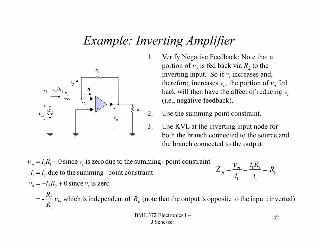
142
Example: Inverting Amplifier1. Verify Negative Feedback: Note that a
portion of vo is fed back via R2 to the inverting input. So if vi increases and, therefore, increases vo, the portion of vo fed back will then have the affect of reducing vi (i.e., negative feedback).
2. Use the summing point constraint.
3. Use KVL at the inverting input node for both the branch connected to the source and the branch connected to the output
RLvin
R2
R1
vi
vo
-
+
0i1=vin/R1
i2
inverted) :input the toopposite isoutput that the(note oft independen is which -
zero is since 0constraintpoint -summing the todue
constraintpoint -summing the todue zero is since 0
1
2
220
21
11
Lin
i
iin
RvRR
vRivii
vRiv
1
1
11
1
RiRi
ivZ in
in
-+ +
+
-
-

BME 372 Electronics I –J.Schesser
143
Op-amp
• Because we assumed that the Op-amp was ideal, we found that with negative feedback we can achieve a gain which is:
1. Independent of the load2. Dependent only on values of the circuit
parameter3. We can choose the gain of our amplifier by
proper selection of resistors.

BME 372 Electronics I –J.Schesser
144
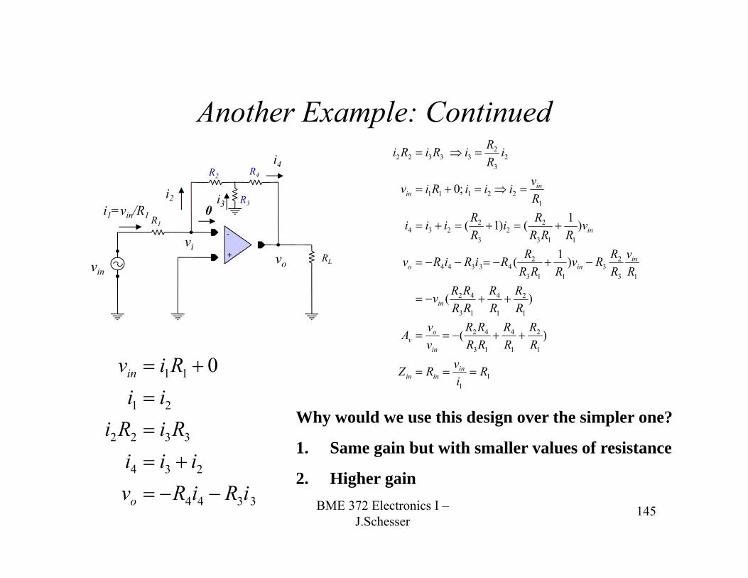
Another Example: Inverting Amplifier1. Verify Negative Feedback:
2. Use the summing point constraint.
3. Use KVL at the inverting input node for the branch connected to the source and KCL & KVL at the node where the 3 resistors are connectedRLvin
R2
R1
vivo
-
+
0i1=vin/R1
i2
3344
234
33223322
21
11
zero is since 0constraintpoint -summing the todue
constraintpoint -summing the todue zero is since 0
iRiRviii
vRiRiRiRivii
vRiv
o
ii
iin
R4
R3
i4
i3
BME 372 Electronics I –J.Schesser
145
Another Example: Continued
RLvin
R2
R1
vivo
-
+
0i1=vin/R1
i2
3344
234
3322
21
11
0
iRiRviii
RiRiii
Riv
o
in
R4
R3
i4
i3
11
1
2
1
4
13
42
1
2
1
4
13
42
13
23
113
243344
113
22
3
2234
122111
23
233322
)(
)(
)1(
)1()1(
;0
RivRZ
RR
RR
RRRR
vvA
RR
RR
RRRRv
Rv
RRRv
RRRRRiRiRv
vRRR
RiRRiii
RviiiRiv
iRRiRiRi
ininin
in
ov
in
inino
in
inin
Why would we use this design over the simpler one?
1. Same gain but with smaller values of resistance
2. Higher gain
BME 372 Electronics I –J.Schesser
146
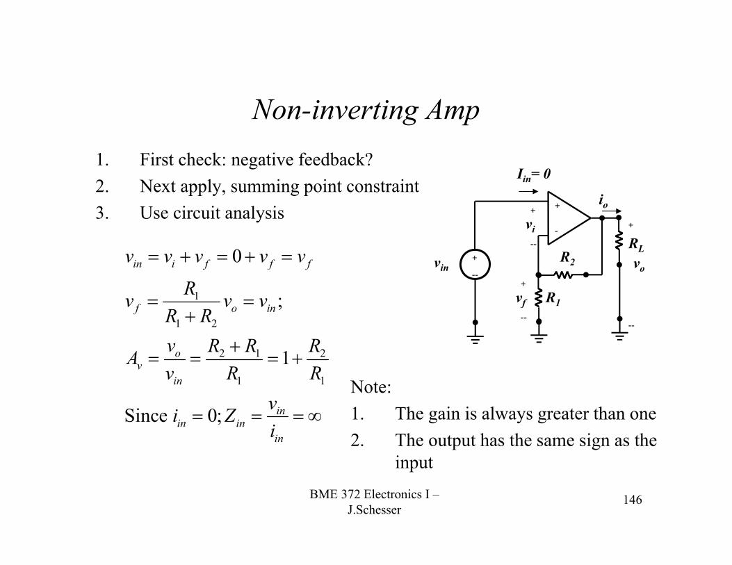
Non-inverting Amp1. First check: negative feedback?2. Next apply, summing point constraint3. Use circuit analysis
+
--vo
+
--
RLR2
R1
+
--
vi
+
--
vf
io
Iin= 0
+
-
vin
1
1 2
2 1 2
1 1
0
;
1
Since 0;
in i f f f
f o in
ov
in
inin in
in
v v v v v
Rv v vR Rv R R RAv R R
vi Zi
Note: 1. The gain is always greater than one2. The output has the same sign as the
input
BME 372 Electronics I –J.Schesser
147
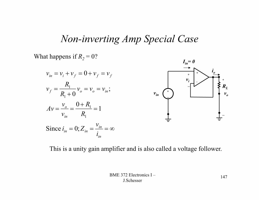
Non-inverting Amp Special CaseWhat happens if R2 = 0?
+
--vo
+
--
RL
+
--
vi
io
Iin= 0
+
-
vin
in
ininin
in
o
inoof
fffiin
ivZi
RR
vvAv
vvvR
Rv
vvvvv
;0 Since
10
;0
0
1
1
1
1
This is a unity gain amplifier and is also called a voltage follower.
BME 372 Electronics I –J.Schesser
148
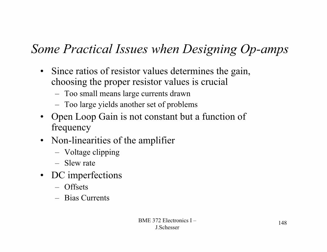
Some Practical Issues when Designing Op-amps• Since ratios of resistor values determines the gain,
choosing the proper resistor values is crucial– Too small means large currents drawn– Too large yields another set of problems
• Open Loop Gain is not constant but a function of frequency
• Non-linearities of the amplifier– Voltage clipping– Slew rate
• DC imperfections– Offsets– Bias Currents
BME 372 Electronics I –J.Schesser
149
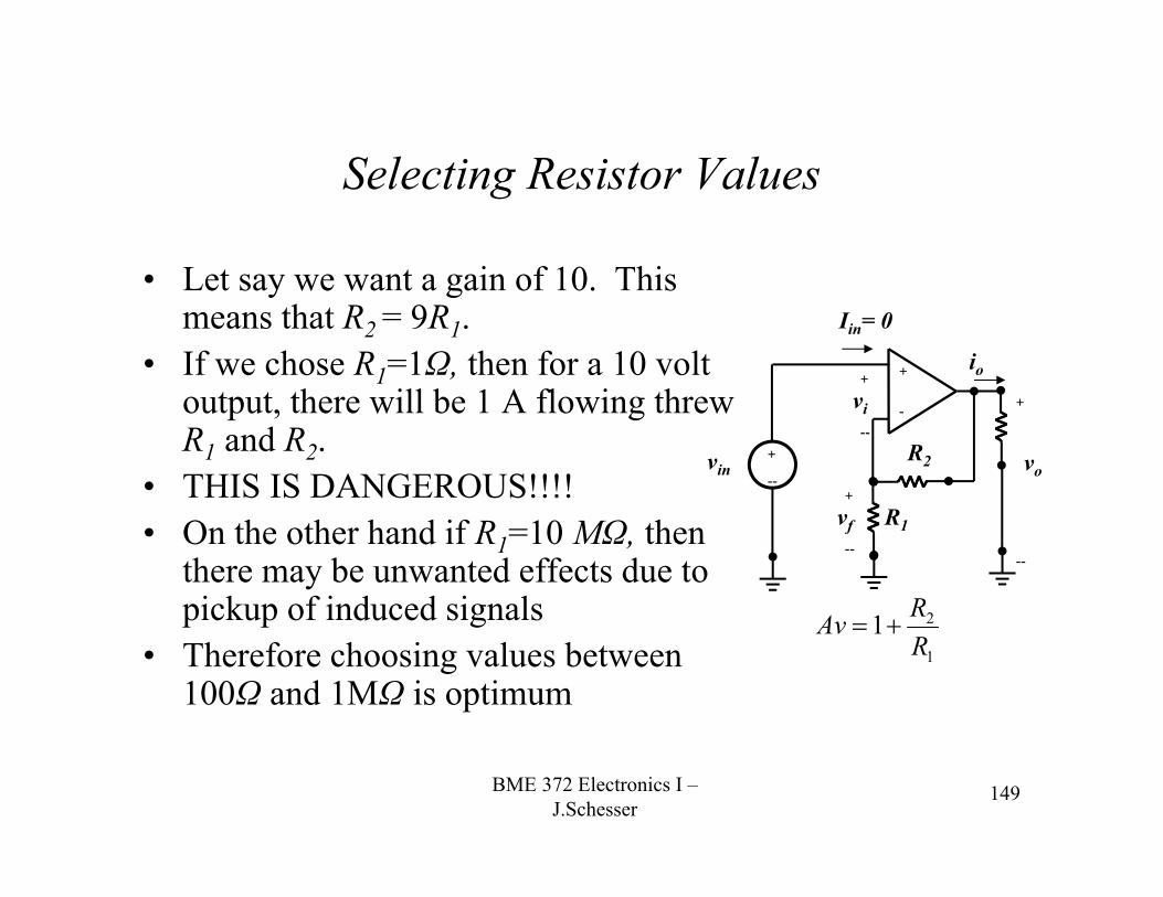
Selecting Resistor Values
• Let say we want a gain of 10. This means that R2 = 9R1.
• If we chose R1=1Ω, then for a 10 volt output, there will be 1 A flowing threw R1 and R2.
• THIS IS DANGEROUS!!!!• On the other hand if R1=10 MΩ, then
there may be unwanted effects due to pickup of induced signals
• Therefore choosing values between 100Ω and 1MΩ is optimum
+
--vo
+
--
R2
R1
+
--
vi
+
--
vf
io
Iin= 0
+
-
vin
1
21RRAv
BME 372 Electronics I –J.Schesser
150
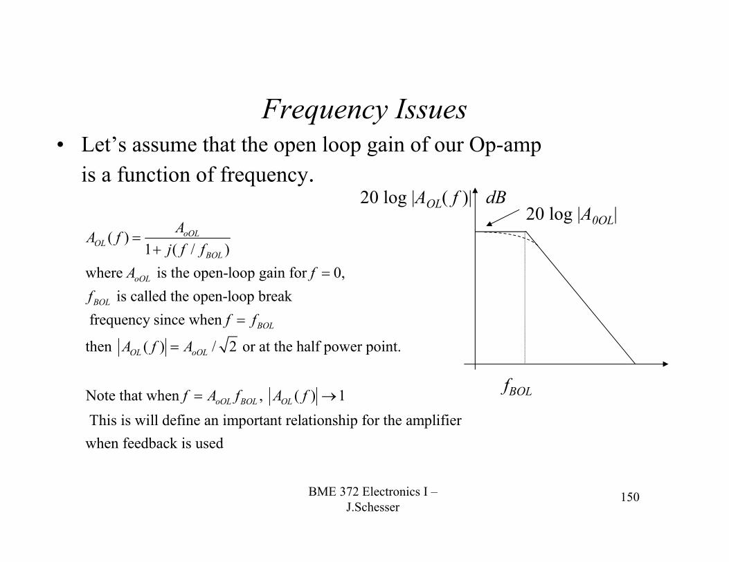
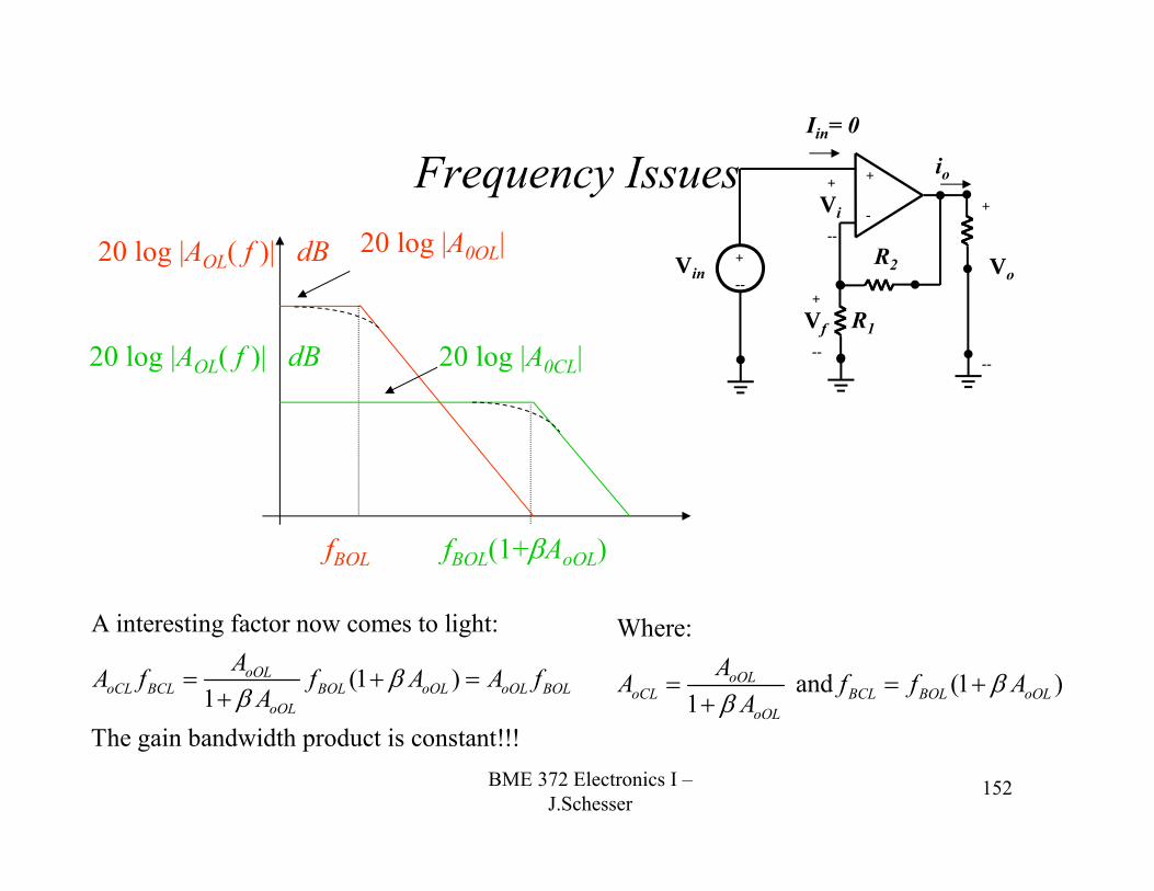
Frequency Issues• Let’s assume that the open loop gain of our Op-amp
is a function of frequency.
( )1 ( / )
where is the open-loop gain for 0, is called the open-loop break
frequency since when
then ( ) / 2 or at the half power point.
Note that when ,
oOLOL
BOL
oOL
BOL
BOL
OL oOL
oOL BOL
AA fj f f
A ff
f f
A f A
f A f A
( ) 1 This is will define an important relationship for the amplifierwhen feedback is used
OL f
20 log |AOL( f )| dB20 log |A0OL|
fBOL
BME 372 Electronics I –J.Schesser
151
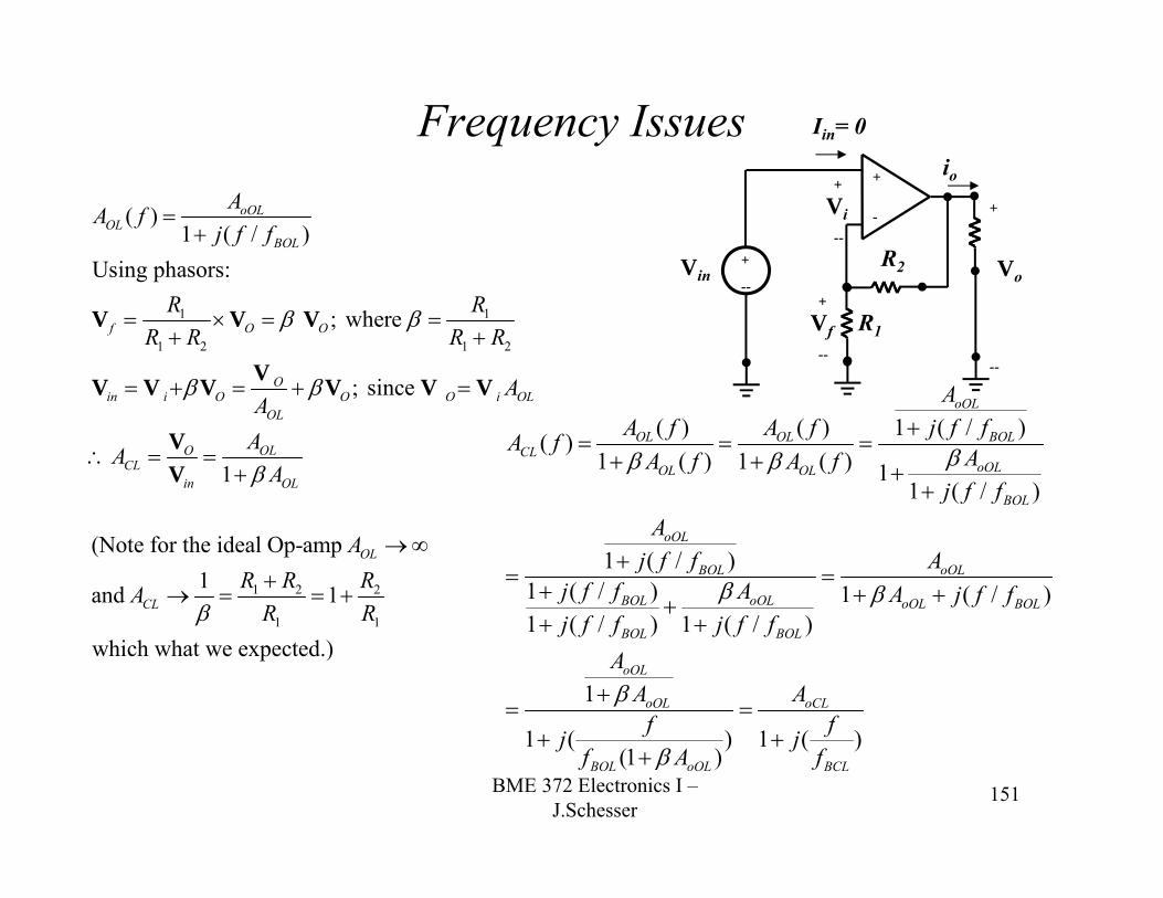
Frequency Issues
1 1
1 2 1 2
1 2 2
1 1
( )1 ( / )
Using phasors:
; where
; since
1
(Note for the ideal Op-amp 1and 1
which what we e
oOLOL
BOL
f O O
Oin i O O O i OL
OL
O OLCL
in OL
OL
CL
AA fj f f
R RR R R R
AA
AAA
AR R RA
R R
V V V
VV V V V V V
VV
xpected.)
+
--Vo
+
--
R2
R1
+
--
Vi
+
--
Vf
io
Iin= 0
+
-
Vin
( ) ( ) 1 ( / )( )1 ( ) 1 ( ) 1
1 ( / )
1 ( / )1 ( / ) 1 ( / )1 ( / ) 1 ( / )
1
1 ( ) 1 ( )(1 )
oOL
OL OL BOLCL
oOLOL OL
BOL
oOL
BOL oOL
BOL oOL oOL BOL
BOL BOL
oOL
oOL oCL
BOL oOL BCL
AA f A f j f fA f AA f A f
j f fA
j f f Aj f f A A j f fj f f j f f
AA A
f fj jf A f
BME 372 Electronics I –J.Schesser
152
Frequency Issues
A interesting factor now comes to light:
(1 )1
The gain bandwidth product is constant!!!
oOLoCL BCL BOL oOL oOL BOL
oOL
AA f f A A fA
+
--Vo
+
--
R2
R1
+
--
Vi
+
--
Vf
io
Iin= 0
+
-
Vin20 log |AOL( f )| dB
fBOL fBOL(1+AoOL)
20 log |A0OL|
20 log |A0CL|20 log |AOL( f )| dB
Where:
and (1 )1
oOLoCL BCL BOL oOL
oOL
AA f f AA
BME 372 Electronics I –J.Schesser
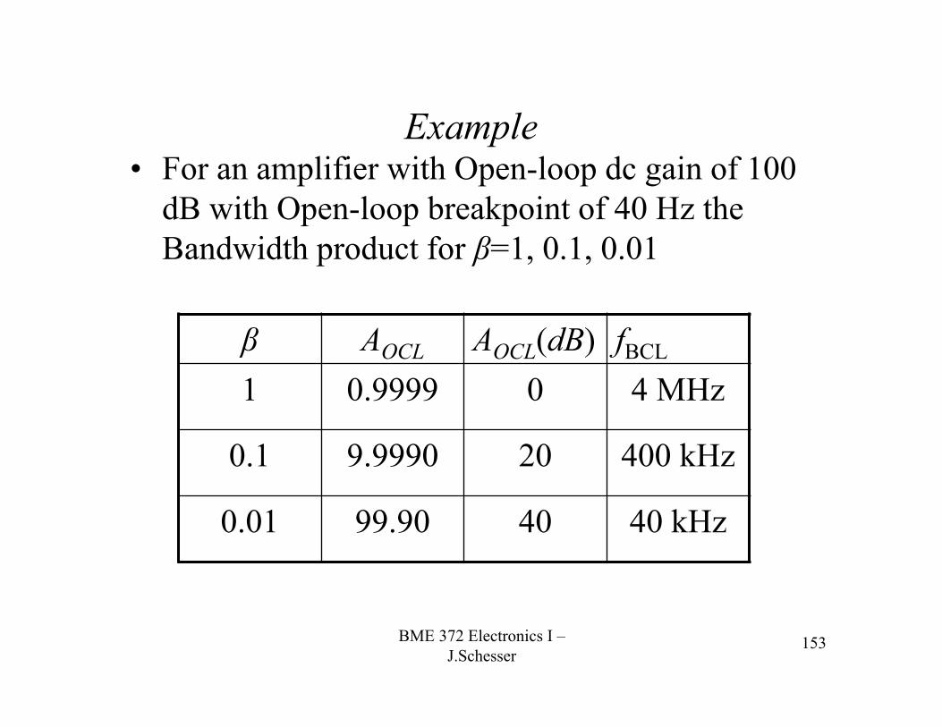
153
Example• For an amplifier with Open-loop dc gain of 100
dB with Open-loop breakpoint of 40 Hz the Bandwidth product for β=1, 0.1, 0.01
β AOCL AOCL(dB) fBCL
1 0.9999 0 4 MHz
0.1 9.9990 20 400 kHz
0.01 99.90 40 40 kHz

BME 372 Electronics I –J.Schesser
154
Voltage clipping
• The Op-amp has a limit as to how large an output voltage and current can be produced. (See figure 2.28)
• For example for the circuit shown it has the following limitations: ±12 V and ±25 mAa) If the load resistor is 10k Ω, what is
the maximum input voltage which can be handled without clipping
b) Repeat for 100 Ω
VVVV
VVmARR
VR
VI
mARR
VR
VIb
in
o
ooo
L
oo
o
L
oo
61.0444.2 44.2
1000300010025
reached. is tageoutput vol maximum beforeoccur llcurrent wioutput maximum case, For this
12310003000
1210012)
max
max
maxmax
21
maxmaxmax
21
maxmaxmax
+
--Vo
+
--
3k
1k
+
--
Vi
+
--
Vf
io
Iin= 0
+
-
Vin
VV
mARR
VR
VIa
A
in
o
L
oo
vCL
3412 reached. iscurrent output maximum before
occur willtageoutput vol maximum case, For this2.4
1000300012
1012)
41/31
max
421
maxmaxmax
-20
-10
0
10
20
0 5 10 15 20
BME 372 Electronics I –J.Schesser
155
Slew Rate
• Slew Rate is a phenomenon which occurs when the Op-Amp can not keep up the change in the input.
• Therefore, we identify the maximum rate of change of the Op-amp as the Slew Rate -SR
BME 372 Electronics I –J.Schesser
156
DC imperfections
• We saw that we have to provide DC voltages to an amplifier in order to provide it with the power to support amplification.– For a differential amplifier which must handle both positive and
negative voltages• The process of designing this DC circuitry is called biasing• As a result, biasing currents flow through the amplifier
which affects its performance. • In particular, a voltage during to the biasing will appear at
the output without any input signal.• These extra voltage can be due to:
– Bias currents flowing in the feedback circuitry– Bias current differentials – Voltage offsets due to the fact that the Op-amp circuitry is not
ideal
BME 372 Electronics I –J.Schesser
157
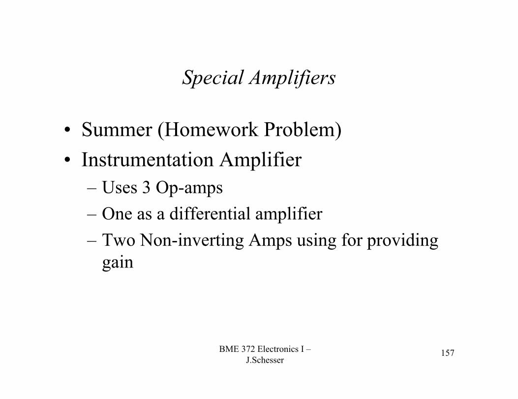
Special Amplifiers
• Summer (Homework Problem)• Instrumentation Amplifier
– Uses 3 Op-amps– One as a differential amplifier– Two Non-inverting Amps using for providing
gain

BME 372 Electronics I –J.Schesser
158
Medical Instrumentation Amplifier
Differential Amplifier
+
--
R2
R1
+
-
v2
+
--
R2
R1
+
-
v1
R3
R4
+
-
vo
R5
R6
Non-inverting Amplifier
Non-inverting Amplifier

BME 372 Electronics I –J.Schesser
159
Medical Instrumentation Amplifier
+
--
R2
R1
+
-
v2
+
--
R2
R1
+
-
v1
R3
R4
vo
R5
R6
Differential Amplifier
Non-inverting Amplifier
Non-inverting Amplifier
v2D
v1D
+
-
BME 372 Electronics I –J.Schesser
160
Medical Instrumentation Amplifier2
6 5
2
6 6 5 5
5 62
6 6 5 5
41
3 4
5 62 41
6 3 4 6 5 5
5 5 6 41 2
6 5 3 4
5 6 4
5 3 4
51 2
6
1 1( )
( )
( )
( )
Chose 1
( )
D x x o
oDx
oDx
y D x i x
oDD
o D D
o D D
v v v vR R
vv vR R R R
R R vv vR R R R
Rv v v v vR R
R R vv R vR R R R R R
R R R Rv v vR R R R
R R RR R R
Rv v vR
R3
R4
vo
R5
R6
Differential Amplifier
v2D
v1D
vx
+
-
4
3
5
6
3564
45356454
43
4
5
65
1 Chose
RR
RR
RRRRRRRRRRRR
RRR
RRR
vi=0
vy

BME 372 Electronics I –J.Schesser
161
Medical Instrumentation Amplifier
+
--
R2
R1
+
-
v2
+
--
R2
R1
+
-
v1
R3
R4
+
-
vo
R5
R6
Differential Amplifier
Non-inverting Amplifier
Non-inverting Amplifier

BME 372 Electronics I –J.Schesser
162
Medical Instrumentation Amplifier
+
--
R2
R1
+
-
v2
+
--
R2
R1
+
-
v1 Non-inverting Amplifier
Non-inverting Amplifier
v2D
v1DvA
AD
AD
AD
AD
vRRv
RRRv
vRRv
RRRv
vRRv
RRRv
Rvv
Rvv
1
21
1
211
1
22
1
212
1
22
12
22
1
2
2
22
Likewise
)11(

BME 372 Electronics I –J.Schesser
163
Medical Instrumentation Amplifier
))(1())((
)]([
)(
21
1
2
6
521
1
21
6
5
1
22
1
21
1
21
1
21
6
5
1
21
1
211
1
22
1
212
21
6
5
vvRR
RRvv
RRR
RRv
vRRv
RRRv
RRv
RRR
RRv
vRRv
RRRv
vRRv
RRRv
vvRRv
o
AAo
AD
AD
DDo
+
--R2
R1
+
-
v2
+
--
R2
R1+
-
v1
R3
R4
vo
R5
R6
Differential Amplifier
Non-inverting Amplifier
Non-inverting Amplifier
+
-
-
+
BME 372 Electronics I –J.Schesser
164
Wheatstone Bridge as a sensor
R3
R4
vo
R2
R1v2D
v1D
+
-rArB
rDrC
V
BME 372 Electronics I –J.Schesser
165
Wheatstone Bridge
Using Thevinin's Theorem on the Wheatstone BridgeLeft side Right side
V2 rB
rB rC
V;r2 rBrC
rB rC
V1 rA
rA rD
V;r1 rArD
rA rD
rArB
rDrC
V
V2 V1
rArB
rDrC
V
V2 V1rA
rB
rDrC
V
V2
V1
r1+V1
--
r2+V2
--
BME 372 Electronics I –J.Schesser
166
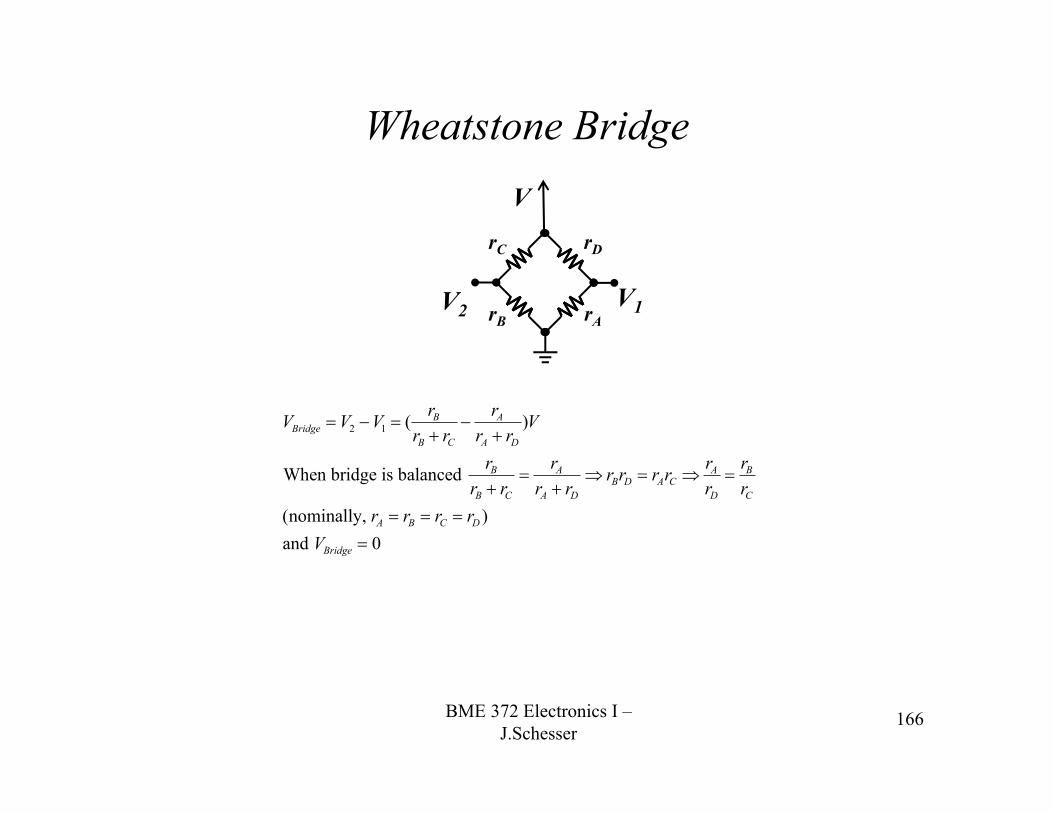
Wheatstone Bridge
VBridge V2 V1 ( rB
rB rC
rA
rA rD
)V
When bridge is balanced rB
rB rC
rA
rA rD
rBrD rArC rA
rD
rB
rC
(nominally, rA rB rC rD )and VBridge 0
rArB
rDrC
V
V2 V1

BME 372 Electronics I –J.Schesser
167
Wheatstone Bridge
V2 vx
R1 r2
vx vo
R2
V2
R1 r2
vx ( 1R1 r2
1R2
) vo
R2
V2
R1 r2
vx (R1 R2 r2
(R1 r2 )R2
) vo
R2
vx vy R4
R3 r1 R4
V1
V2
R1 r2
R4
R3 r1 R4
V1(R1 R2 r2
(R1 r2 )R2
) vo
R2
V2
R1 r2
R4
R3 r1 R4
(R1 R2 r2
R2
)V1
(R1 r2 )vo
R2
vo R2
R1 r2
[(R4
R3 r1 R4
)(R1 R2 r2
R2
)V1 V2 ]
Chose R1 R2 r2
R2
R4
R3 r1 R4
1
vo R2
R1 r2
(V1 V2 ) R2
R1 r2
(rA
rA rD
rB
rB rC
)V
R3
R4
vo
R2
R1 +
-
r1+V1
--
r2+V2
--
vx

BME 372 Electronics I –J.Schesser
168
Wheatstone Bridge
R3
R4
vo
R2
R1 +
-
r1+V1
--
r2+V2
--
Chose R1 R2 r2
R2
R4
R3 r1 R4
1
R1 R2 r2
R2
R3 r1 R4
R4
R1 R2 rBrC
rB rC
R2
R3
rArD
rA rD
R4
R4
Hard to deal with; then let's make sure that r2 R1 R2 and r1 R3 R4
R1 R2
R2
R3 R4
R4
R2R3 R2R4 R4R1 R4R2 R2R3 R4R1
R4
R3
R2
R1
vo R2
R1
(rA
rA rD
rB
rB rC
)V
Note that the output depends on the unbalance of the bridge and when the bridge is balanced vo 0
Gain is still R2
R1
vx
BME 372 Electronics I –J.Schesser
169
Integrators and Differentiators
t
in
t
o
in
dxxvRC
dxxiC
v
tiR
tvti
002
21
)(1)(1
)()()(
vin
C
R
vi
vo
-
+
0i2i1
vin
R
C
vi
vo
-
+
0i2i1
dttdvRCRtiv
tidt
tCdvti
ino
in
)()(
)()()(
2
21
BME 372 Electronics I –J.Schesser
170
Frequency Analysis
vin
vivo
-
+
0i1=vin/Z1
i2
1in
o
Lin1
o
1
11in
ZZ
VV
ZVZZ
ZIVII
ZIV
2
2
22
2
- )()(
oft independen is which )(-
zero )(virtually is since 0)()(constraintpoint -summing the todue )()(
zero )(virtually is since 0)()()(
jj
j
vjjjj
vjjj
i
i
ZLvin
C
R
vivo
-+
0i1=vin/Z1 i2
ZLvin
R
C
vivo
-+
0i1=vin/Z1 i2
integratoran 1- )()( 2
RCjjj
1in
o
ZZ
VV tordifferenia a - )(
)( 2 RCjjj
1in
o
ZZ
VV
Z2
Z1

BME 372 Electronics I –J.Schesser
171
Frequency Response
vin
CR
vi
vo
-
+
0i2i1
vin
RC
vi
vo
-
+
0i2i1
1- )()( 2
RCjjj
1in
o
ZZ
VV
RCjjj
1in
o
ZZ
VV 2-
)()(
ω
ω

BME 372 Electronics I –J.Schesser
172
Frequency Response
vin
C2R1
vi
vo
-
+
0i2i1
vin
R2
C1vi
vo
-
+
0i2
i1
R2 12 2 21 12
1 1 2 2 1 1 1
1 1 tan ( )(1 ) 1 ( )
out
in
V Z R R C RV Z R j C R R C R
0
500
1,000
1,500
2,000
2,500
1.E+00 1.E+02 1.E+04 1.E+06 1.E+08HZ
R1 51 C1 10mf R2 100k
R1
Vout
Vin
Z2
Z1
R2
R1
jC1R1
(1 jC1R1)
R2
R1
C1R1
1 (C1R1)2
2 tan1(C1R1)
0
500
1,000
1,500
2,000
2,500
1.E+00 1.E+02 1.E+04 1.E+06 1.E+08HZ
R1 51 C1 10mf R2 100k
BME 372 Electronics I –J.Schesser
173
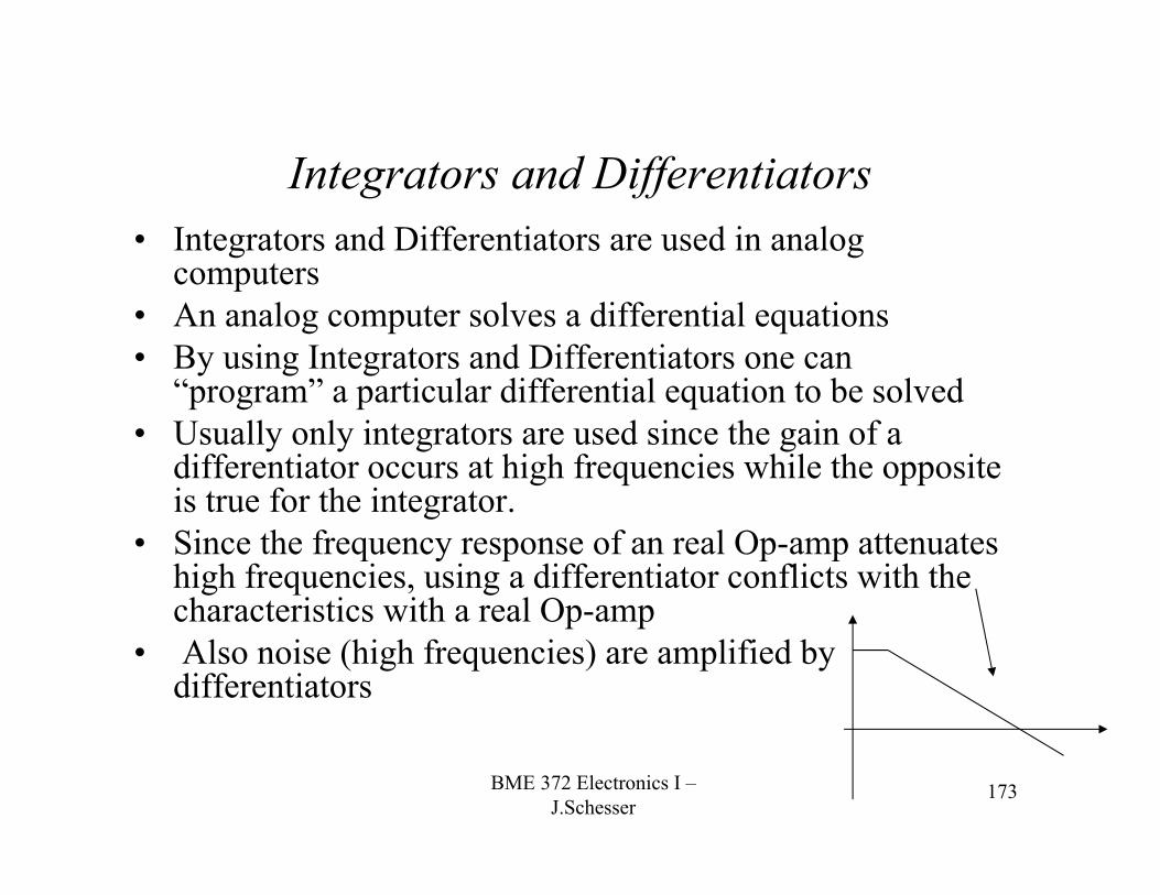
Integrators and Differentiators• Integrators and Differentiators are used in analog
computers• An analog computer solves a differential equations• By using Integrators and Differentiators one can
“program” a particular differential equation to be solved• Usually only integrators are used since the gain of a
differentiator occurs at high frequencies while the opposite is true for the integrator.
• Since the frequency response of an real Op-amp attenuates high frequencies, using a differentiator conflicts with the characteristics with a real Op-amp
• Also noise (high frequencies) are amplified by differentiators
BME 372 Electronics I –J.Schesser
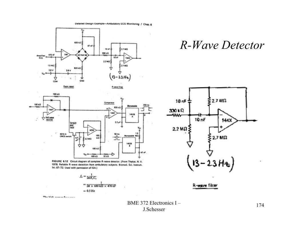
174
R-Wave Detector

BME 372 Electronics I –J.Schesser
175
Positive Feedback• What happens to our Op-amp circuit if positive
feedback is used?
• Even if vin = 0 and there is a slight voltage at vi then – vo = AOLvi will increase vi– vo will grow even larger– Eventually this will reach an extreme since there is not
infinite energy in the circuit
RLvin
R
R
vivo
+
-
iini1
i2
) (21)(
21
gain loopopen theis where
0
impedanceinput infinite hasAmplifier since ;00
:input at the KCL Using
21
iOLinoini
OLiOLo
oiini
in
in
vAvvvv
AvAvR
vvR
vvi
iii
BME 372 Electronics I –J.Schesser
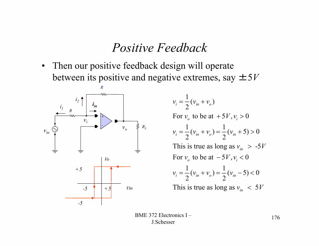
176
Positive Feedback• Then our positive feedback design will operate
between its positive and negative extremes, say ±5V
RLvin
R
R
vivo
+
-
iini1
i21 ( )2
For to be at 5 , 01 1( ) ( 5) 02 2
This is true as long as -5For to be at 5 , 0
1 1( ) ( 5) 02 2
This is true as long as 5
i in o
o i
i in o in
in
o i
i in o in
in
v v v
v V v
v v v v
v Vv V v
v v v v
v V
-5 +5
-5
+5
Vin
Vo
BME 372 Electronics I –J.Schesser
177
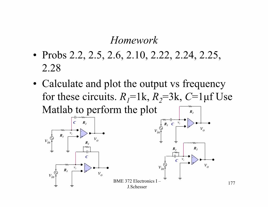
Homework• Probs 2.2, 2.5, 2.6, 2.10, 2.22, 2.24, 2.25,
2.28• Calculate and plot the output vs frequency
for these circuits. R1=1k, R2=3k, C=1μf Use Matlab to perform the plot
vin
C
R1vi
vo
-
+
R2
vin
CR1vi
vo
-
+
R2
vin
C
R1vi
vo
-
+
R2
vin
C
R1
vi
vo
-
+
R2

BME 372 Electronics I –J.Schesser
178
Homework
rA= R-ΔR
rB = R+ΔR
rD=R+ΔRrC=
R-ΔR
V
V2 V1
Wheatstone Bridge - Strain Gauge• A strain gauge shown here is used with a difference amplifier. Calculate the
amplifier output signal as a function of ΔR and difference amplifier resistors. Assume that ΔR<<R.
• For the strain gauge calculate the value of each of the difference amplifier resistors for a value of R=10Ω and a percent change in R of ±10% if the output of the amplifier is less than ±5 volts. Assume that the bridge is powered with 5 volts.
BME 372 Electronics I –J.Schesser
179
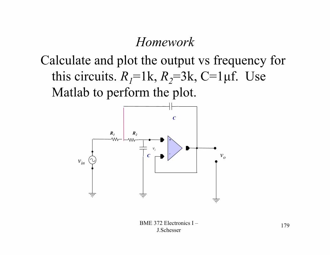
HomeworkCalculate and plot the output vs frequency for
this circuits. R1=1k, R2=3k, C=1μf. Use Matlab to perform the plot.
vin
C
R1
vi
vo
+
-
R2
C