LEEF model 2, version 1
111
R. G. Sparber December 3, 2014 Page 1 of 111 Lathe Electronic Edge Finder, Model 2 Lathe Electronic Edge Finder, Model 2, version 1.0 By R. G. Sparber Copyleft protects this document. 1 Introduction The Lathe Electronic Edge Finder (LEEF) is able to detect the cutter coming in contact with the workpiece. No modification to the lathe, cutter, or workpiece is needed 2 . One magnetic probe is placed onto the chuck and another one near the cutter. An LED lights when the tip of the cutter just touches the surface of the workpiece. This task would be very simple if the cutter was insulated from the rest of the lathe. But in most cases, this is not an attractive solution. The LEEF is intended to be used on a previously turned surface. For example, a work piece is chucked up and turned true. Then there is call for a change in cutters. By changing the cutter, the initial zero set is likely lost. By using the LEEF, you quickly reestablish zero with the new cutter. Since there is no need for the user to see the point of contact between cutter and workpiece, the LEEF can also be used with a boring bar to touchdown at the bottom of a hole. 1 You are free to copy and distribute this document but not change it. My intent is to do defensive publishing (http://en.wikipedia.org/wiki/Defensive_publication). 2 Cutter and workpiece must be electrically conductive.
Transcript of LEEF model 2, version 1

R. G. Sparber December 3, 2014 Page 1 of 111 Lathe Electronic Edge Finder, Model 2
Lathe Electronic Edge Finder, Model 2,
version 1.0
By R. G. Sparber
Copyleft protects this document.1
Introduction The Lathe Electronic Edge
Finder (LEEF) is able to
detect the cutter coming in
contact with the workpiece.
No modification to the
lathe, cutter, or workpiece
is needed2. One magnetic
probe is placed onto the
chuck and another one near
the cutter. An LED lights
when the tip of the cutter
just touches the surface of
the workpiece.
This task would be very simple if the cutter was insulated from the rest of the lathe.
But in most cases, this is not an attractive solution.
The LEEF is intended to be used on a previously turned surface. For example, a
work piece is chucked up and turned true. Then there is call for a change in cutters.
By changing the cutter, the initial zero set is likely lost. By using the LEEF, you
quickly reestablish zero with the new cutter.
Since there is no need for the user to see the point of contact between cutter and
workpiece, the LEEF can also be used with a boring bar to touchdown at the
bottom of a hole.
1 You are free to copy and distribute this document but not change it. My intent is to do defensive publishing
(http://en.wikipedia.org/wiki/Defensive_publication). 2 Cutter and workpiece must be electrically conductive.

R. G. Sparber December 3, 2014 Page 2 of 111 Lathe Electronic Edge Finder, Model 2
This article is part of a series
3 that explains the problem being solved, previous
iterations of this circuit, plus shop performance. I will focus only on this new
design. To see the LEEF in action, watch the video at
http://www.youtube.com/watch?v=4ilY9Pse7TU&feature=youtu.be
This is my prototype.
The next iteration was a single sided circuit board:
This is a computer generated picture created by Mark
Cason showing one version of the finished product.
The board is 50 mm on a side. Not shown is the top
side ground plane.
This is the first hand etched and drilled prototype
that used almost the same artwork except is single
sided. I didn't have an amber LED so used a green
one for the center LED.
3 See http://rick.sparber.org/ueef.pdf for a description of the problem being solved. See
http://rick.sparber.org/ma.htm#6 for the complete set of articles.

R. G. Sparber December 3, 2014 Page 3 of 111 Lathe Electronic Edge Finder, Model 2
The LEEF detects the change in resistance between cutter and workpiece caused
by the cutter coming in contact with the workpiece. No modification to the lathe is
needed. The resistance before touchdown can be as low as 0.01 ohms or as high as
1.4 ohm. This is essentially the resistance of the spindle bearings. The test current
is 20 mA. Induced 60 Hz noise can be 40 times larger than the signal being
detected.
A LEEF, Model 1 also exists. It performs the same task as the design presented in
this article but has a minimum resistance threshold of 2 ohms. If your machine has
a spindle bearings resistance above 2 ohms, then the Model 1 is a better choice. It
is easier to use and costs much less than the Model 2. For details see
http://rick.sparber.org/LEEF_Model_1.pdf
R. G. Sparber December 3, 2014 Page 4 of 111 Lathe Electronic Edge Finder, Model 2
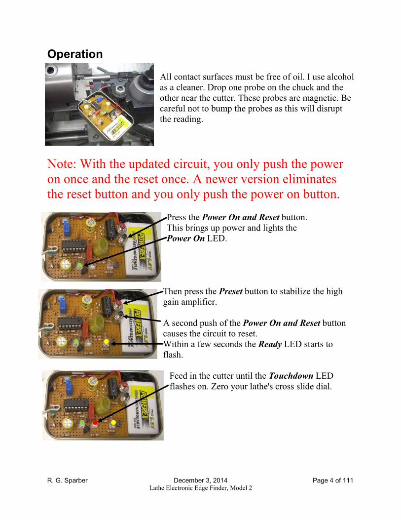
Operation
All contact surfaces must be free of oil. I use alcohol
as a cleaner. Drop one probe on the chuck and the
other near the cutter. These probes are magnetic. Be
careful not to bump the probes as this will disrupt
the reading.
Note: With the updated circuit, you only push the power
on once and the reset once. A newer version eliminates
the reset button and you only push the power on button.
Press the Power On and Reset button.
This brings up power and lights the
Power On LED.
Then press the Preset button to stabilize the high
gain amplifier.
A second push of the Power On and Reset button
causes the circuit to reset.
Within a few seconds the Ready LED starts to
flash.
Feed in the cutter until the Touchdown LED
flashes on. Zero your lathe's cross slide dial.

R. G. Sparber December 3, 2014 Page 5 of 111 Lathe Electronic Edge Finder, Model 2
If you wish to repeat the touchdown event, back
the cutter out and press the
Power On and Reset button again. The
Ready LED will start to flash within a few
seconds to say the LEEF is ready to detect another
touchdown event.
When done, remove the probes from the lathe which also turns off LEEF power.
The Ready and Touchdown LED tell you
about your shop environment and machine. If
the Ready LED (shown here in amber) is
steady, it says you have no electrical noise
induced in your machine or your spindle
resistance is greater than 1.3 ohms. The more it
flickers, the more noise you have. If the flicker
rate is constant, then your noise is constant. If
it is random, you have a lot of voltage spikes.
Spikes are commonly generated by motors
turning on and off quickly. Excessive noise
will interfere with proper circuit operation.
The Touchdown LED (shown here in red) in conjunction with the Ready LED tells
you about your machine. If you touchdown, see the touchdown LED flash, and
back away from touchdown, the time it takes before the Ready LED starts to flash
again will tell you about your spindle resistance. The longer this time delay, the
larger the resistance. A time delay of 3 seconds correlates to the minimum spindle
resistance and maximum contact resistance between cutter and workpiece. The
longer the time delay, the larger the spindle resistance. Of course, normally you
would press the reset button if the wait time became excessive.
If at touchdown both the Ready and Touchdown LEDs turn on, your spindle
resistance is greater than 1.4 ohms. This just means that you probably could have
used the LEEF, Model 1 which cost less and is easier to use.
The power on LED (shown in green) will come on even when the battery is too
low for the circuit to work. So if the LEEF begins to behave abnormally, try
replacing the battery. Given a 200 mA-H battery, you should get about 8 hours of
run time from a battery.

R. G. Sparber December 3, 2014 Page 6 of 111 Lathe Electronic Edge Finder, Model 2
Requirements and Goal My design requirements were:
1. Be able to detect the touchdown down of the cutter on the workpiece when
the spindle resistance is as small as 0.01 ohms and the contact resistance of
the cutter on the workpiece is no greater than 0.6 ohms.
2. Maximum spindle resistance shall be 1 ohm.
3. Be able to detect touchdown even when 100 microvolts of 60 Hz is present
across the unknown resistance.
4. Test current less than 25 mA.
5. Open circuit test voltage less than 9V.
6. Automatic power down.
7. Less than 10 seconds delay from power up until ready to detect.
8. Less than 10 seconds delay from previous touchdown event until ready to
detect again.
9. Visual indication of the circuit's state
a. Power
b. Ready to detect
c. Touchdown
10. Run on a single 9V battery.
My design goal were
1. minimize the complexity and cost of the circuit.
2. Detect touchdown for spindle resistances greater than 1 ohm and contact
resistance of the cutter on the workpiece of no greater than 0.6 ohms.
With the latest updates, I can now detect resistances above 5 ohms and still see the
READY LED light before touchdown.

R. G. Sparber December 3, 2014 Page 7 of 111 Lathe Electronic Edge Finder, Model 2
Background Many problems had to be solved in order to make a circuit that could detect
touchdown when the spindle resistance is as low as 0.01 ohms and the contact
resistance is no more than 0.6 ohms. This situation causes a change in resistance of
as little as 163 micro ohms. Furthermore, it has to do it in an industrial
environment which has a high level of 60 Hz noise. The journey of this
development was very much like pealing an onion. I would solve one problem,
cause or reveal a new one, and then start the cycle over. Eventually I did get to the
point where all known problems were solved and no new ones became evident.
That does not mean that new problems won't pop up in the future.
The circuit is reacting to an input as small as 3.2 micro volts. This demands special
attention to board layout to minimize internal noise pick up and DC voltage drops
across critical circuit paths. Yet I had to connect the high sensitivity parts of the
circuit to the high noise generating parts without unwanted interactions. At one
point in the circuit I have a voltage transition of 8V yet if it generated a 1.6
microvolt spike at the input, the LEEF would not operate correctly.
I was extremely fortunate to have Mark Cason designing the layout. The layout is
the single most important analog component.

R. G. Sparber December 3, 2014 Page 8 of 111 Lathe Electronic Edge Finder, Model 2
Contents
Introduction ................................................................................................................ 1
Operation .................................................................................................................... 4
Requirements and Goal .............................................................................................. 6
Background ................................................................................................................ 7
Limitations ................................................................................................................. 9
Theory and Practice .................................................................................................10
Isn't It Just an Ohm Meter? ......................................................................................10
Drop The Test Current Down ..................................................................................11
Add A Voltage Amplifier ........................................................................................12
Block What I Don't Want .........................................................................................13
A Negative Peak Detector ........................................................................................15
Pulse Amplifier and LED Driver .............................................................................16
Machine Shops are Nasty Places .............................................................................18
Using a Good Idea Twice ........................................................................................19
The Schematic ..........................................................................................................20
Parts List By Name ..................................................................................................21
Parts List By Quantity and Names ...........................................................................23
Mouser Bill Of Materials .........................................................................................25
Single Sided Circuit Board Artwork ........................................................................26
Detailed View ..........................................................................................................29
Touchdown Sensing Physics ....................................................................................30
Power Control ..........................................................................................................31
The First Gain Stage ................................................................................................41
Update to First Stage ................................................................................................43
The Second Gain Stage ............................................................................................46
The Negative Peak Detector with Update ................................................................47
The Ready LED .......................................................................................................63
Blocking Capacitor, Comparator, and Touchdown LED ........................................64
The COM Node ........................................................................................................66
Preset and Reset .......................................................................................................69

R. G. Sparber December 3, 2014 Page 9 of 111 Lathe Electronic Edge Finder, Model 2
The Power On and Off Sequence.............................................................................83
Time Constants ........................................................................................................87
Simulating the Circuit ..............................................................................................90
Scope Pictures ..........................................................................................................95
Possible Future Improvements ...............................................................................105
Acknowledgements ................................................................................................106
Appendix: The LT1014 Op Amp ...........................................................................107
Limitations All designs have limitations. In this case, I am trying to detect a very tiny drop in
voltage while a large amount of AC noise is present. Any noise that drops in level
over a brief amount of time may look identical to the signal I am trying to process.
So given an environment with a lot of voltage spikes, the circuit might not work
unless its sensitivity is reduced.
Such is the case around at least some CNC machines. My limited experience with
these machines tells me I might be able to ignore their spikes but can't guarantee it.
Filtering in my circuit that would block these spikes would also tend to block the
signal I am trying to detect. An alternative is to set the threshold so it takes a
bigger change in resistance to trigger a touchdown indication. So we are up against
the physics of it4 and any solution must first change the situation so different
conditions exists. It is a classic case of "if you can't solve the problem, change the
problem".
The circuit can function correctly until the spindle resistance gets above 1 ohm.
Above 1 ohm, the circuit will still detect touchdown as long as the touchdown
contact resistance is no more than 0.6 ohms. The touchdown indication will be
different: the Ready LED will not flash to indicate the circuit is ready to detect
touchdown. Then at touchdown, both the Touchdown and Ready LEDs light at
the same time. Do understand that if you have a spindle resistance above 1 ohm, a
much simpler circuit will do the job. See http://rick.sparber.org/rctf.pdf for details.
4 By this I mean up against things that cannot be solved.

R. G. Sparber December 3, 2014 Page 10 of 111 Lathe Electronic Edge Finder, Model 2
Theory and Practice You can find the complete schematic on page 20. Leading up to this point, I will
present the design evolution and theory.
Isn't It Just an Ohm Meter? I am just trying to measure a resistance. To do
this I have a DC voltage, Vcc which feeds
through a resistor, R1, and into my unknown
resistance, Rx. A test current, Ix, flows. Between
test probes "S" and G" I am able to measure the
resulting voltage across my unknown resistance.
It is called Vx.
�� = �� × �� (1)
So if I simply generate Ix and measure Vx, I can
calculate Rx.
�� = �
Rx has two values. Before touchdown it can be as
small as 0.01 ohms. After touchdown it can be as small as 0.009836 ohms.
If Ix = 1 amp, then
�� = �� × �� �� = 0.01�ℎ�� × 1��� �� = 0.01�����
So before touchdown we measure 0.01 volts. After touchdown Rx equals 0.009836
ohms which generates 0.009836 volts when 1 amp flows through it. Although
these are tiny voltages, it is possible to measure them with a good Digital Volt
Meter.
We have solved the problem of detecting touchdown but created a new one.
Passing 1 amp through bearings can cause damage due to arcing.

R. G. Sparber December 3, 2014 Page 11 of 111 Lathe Electronic Edge Finder, Model 2
Drop The Test Current Down OK, let's drop the test current down to a more reasonable level. How about 0.02
amps which can also be written as 20 milli amps or 20 mA? From equation (1) we
can calculate Vx again.
�� = �� × �� (1)
�� = 0.01�ℎ�� × 20��
�� = 0.0002�������200����������
Damn! Now this is a very tiny voltage. Furthermore, after touchdown we will see
�� = 0.009836�ℎ�� × 20��
�� = 0.0001967�������196.7����������
a change of only 3.28 micro volts. To give you an idea how tiny this is, consider
that the voltage picked up from a small radio antenna is just a few micro volts.
We have solved the problem of detecting touchdown without damaging the
bearings but created a new one. How do we detect these two tiny voltages that are
so close together?

R. G. Sparber December 3, 2014 Page 12 of 111 Lathe Electronic Edge Finder, Model 2
Add A Voltage Amplifier
OK, let's use a voltage amplifier to raise the voltage back up to a reasonable value.
My voltage amplifier will take the voltage Vx and multiply it by a constant I call
G, for gain (not to be confused with test probe "G", for ground). The resulting
voltage, Vout , will follow the equation
�!"# = �� × $
�!"# = %�� × ��& × $ (2)
If I pick a gain, G, of 10,000, then my pre-touchdown Vout will be
�!"# = %�� × ��& × $ �!"# = %0.01�ℎ�� × 20��& × 10,000 �!"# = %200���������� × 10,000& �!"# = 2�����
And after touchdown my Vout will be 1.97 volts.
We have solved the problem of measuring a tiny Vx but now have a new problem.
What if my pre-touchdown resistance changes just a little. I will then get a
different Vout. I would have to record this pre-touchdown voltage and use it to
determine if my touchdown voltage was right. That sounds like an annoying bit of
work.
R. G. Sparber December 3, 2014 Page 13 of 111 Lathe Electronic Edge Finder, Model 2
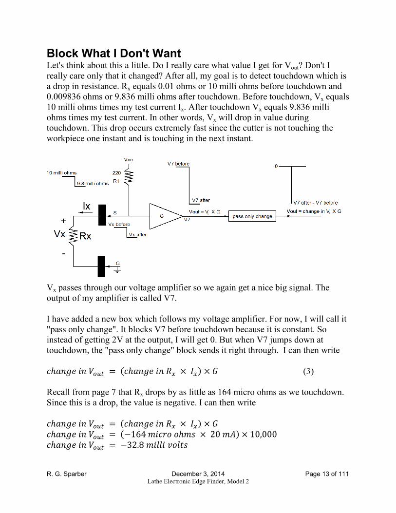
Block What I Don't Want Let's think about this a little. Do I really care what value I get for Vout? Don't I
really care only that it changed? After all, my goal is to detect touchdown which is
a drop in resistance. Rx equals 0.01 ohms or 10 milli ohms before touchdown and
0.009836 ohms or 9.836 milli ohms after touchdown. Before touchdown, Vx equals
10 milli ohms times my test current Ix. After touchdown Vx equals 9.836 milli
ohms times my test current. In other words, Vx will drop in value during
touchdown. This drop occurs extremely fast since the cutter is not touching the
workpiece one instant and is touching in the next instant.
Vx passes through our voltage amplifier so we again get a nice big signal. The
output of my amplifier is called V7.
I have added a new box which follows my voltage amplifier. For now, I will call it
"pass only change". It blocks V7 before touchdown because it is constant. So
instead of getting 2V at the output, I will get 0. But when V7 jumps down at
touchdown, the "pass only change" block sends it right through. I can then write
�ℎ�()*�(�!"# = %�ℎ�()*�(�� × ��& × $ (3)
Recall from page 7 that Rx drops by as little as 164 micro ohms as we touchdown.
Since this is a drop, the value is negative. I can then write
�ℎ�()*�(�!"# = %�ℎ�()*�(�� × ��& × $ �ℎ�()*�(�!"# = %−164������ℎ�� × 20��& × 10,000 �ℎ�()*�(�!"# = −32.8����������

R. G. Sparber December 3, 2014 Page 14 of 111 Lathe Electronic Edge Finder, Model 2
So as long as I see a drop in Vout of at least 32.8 milli volts, I will know we had
touchdown. Now here is the cool part: I don't care what value I have for Rx. It will
vary between machines. I only need to know if Vout drops by at least 32.8 milli
volts and I will be sure we had touchdown.
Well, we almost got it. Vout is a very narrow spike with an amplitude of -32.8 milli
volts. I would have trouble trying to see it if an LED was driven from this voltage.
I need to make it wider and taller.

R. G. Sparber December 3, 2014 Page 15 of 111 Lathe Electronic Edge Finder, Model 2
A Negative Peak Detector
We will first work on making the signal wider. This new function always responds
to the most negative peak voltage that comes along.
Before touchdown, the negative peak detector sees zero volts so that is what it
outputs. But then the spike appears with its amplitude of -32.8 milli volts. This is
now the most negative peak so becomes the new output. When the spike is over,
the negative peak detector again sees zero volts. Since this new input is smaller
than the spike, the output remains at the spike level.
In this way, we have greatly widened the spike into a constant value. It is still only
a drop of 32.8 milli volts so we still need to make it bigger.
There are many ways to convert a spike into a level. You will later see why using a
negative peak detector was a good choice.
R. G. Sparber December 3, 2014 Page 16 of 111 Lathe Electronic Edge Finder, Model 2
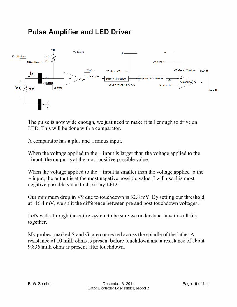
Pulse Amplifier and LED Driver
The pulse is now wide enough, we just need to make it tall enough to drive an
LED. This will be done with a comparator.
A comparator has a plus and a minus input.
When the voltage applied to the + input is larger than the voltage applied to the
- input, the output is at the most positive possible value.
When the voltage applied to the + input is smaller than the voltage applied to the
- input, the output is at the most negative possible value. I will use this most
negative possible value to drive my LED.
Our minimum drop in V9 due to touchdown is 32.8 mV. By setting our threshold
at -16.4 mV, we split the difference between pre and post touchdown voltages.
Let's walk through the entire system to be sure we understand how this all fits
together.
My probes, marked S and G, are connected across the spindle of the lathe. A
resistance of 10 milli ohms is present before touchdown and a resistance of about
9.836 milli ohms is present after touchdown.

R. G. Sparber December 3, 2014 Page 17 of 111 Lathe Electronic Edge Finder, Model 2
I pass a test current, Ix, out my "S" probe". It flows through the unknown
resistance, Rx and returns via the "G" probe. The flow of current generates a
voltage, Vx.
Before touchdown, Vx is at one value. After touchdown it is at a smaller value
because Rx is smaller when the cutter contacts the work piece. Vx is fed into my
voltage amplifier where it is multiplied by a value called G. The result is a much
larger voltage at V7 that is one value before touchdown and a lower value after
touchdown.
The voltage step down at V7 feeds into a "pass only change" function that blocks
the constant voltage before and after touchdown. It only passes the change which
will be a very narrow spike. Before and after this spike the output voltage is zero.
The amplitude of this spike equals the voltage at V7 after touchdown minus the
voltage at V7 before touchdown. In the ideal case, this spike is zero seconds wide.
Not too useful at this point.
The spike is fed into a negative peak detector which holds the most negative
voltage it sees. So before touchdown it outputs zero at V9. In response to the spike,
it outputs the peak of our spike. After touchdown it continues to output the peak of
our spike.
V9 feeds into a comparator. When V9 is greater than a specified threshold, we turn
an LED off. When V9 is less than this threshold, the LED turns on. In this way our
touchdown event turns on an LED so the user knows to stop feeding the cutter into
the workpiece.
It sounds like this may actually work. But alas, there are perils in a machine shop.

R. G. Sparber December 3, 2014 Page 18 of 111 Lathe Electronic Edge Finder, Model 2
Machine Shops are Nasty Places
Consider what happens when there is electrical noise. If I have some AC voltage
getting into Vx, it will be added to the drop in voltage caused by touchdown. Then
the combination will be amplified by G. And since it is constantly changing, the
amplified AC noise5 will get through our "pass only change" box.
But then things start to get better. Our negative peak detector holds the most
negative value of V9 before touchdown. So instead of AC, we get a constant value
that sits on the "underside" of the noise. No matter how large the AC noise, we will
always end up on this underside.
Then comes the spike. The negative peak detector grabs the tip of the spike and
holds that value. But soon after the spike comes the next negative peak of the noise
so our post-touchdown voltage just got a little larger.
From there, V9 feeds into the comparator . Oops, a problem. Due to the AC noise,
my threshold voltage is no longer centered. In fact, given a large enough level of
noise, I could exceed the threshold before touchdown. Then I would be unable to
detect touchdown.
5 The noise does not have to be a sine wave, it just has to be relatively constant. So a series of pulses would work
here too as long as the amplitude did not change too much.

R. G. Sparber December 3, 2014 Page 19 of 111 Lathe Electronic Edge Finder, Model 2
Using a Good Idea Twice
Thinking back to page 14, we talked about how the "pass only change" function
was able to block the pre-touchdown voltage and substitute zero. It then passed
only the change. Well, we need it again. V9 was shifted downward by the AC
noise so our threshold is no longer centered.
Going into our second "pass only change" block is V9. Coming out is a negative
pulse that represents touchdown. And as before, it is just a skinny pulse. Too
narrow to flash the LED. This time we don't need a negative peak detector. Instead,
we will use a pulse stretcher. The pulse stretcher takes this narrow pulse and makes
it slightly wider. This wider pulse feeds into our comparator with its threshold
voltage. We get out a signal able to drive our LED that is easy to see.
We have just completed a tour of the main functions of the Lathe Electronic Edge
Finder. I tried hard to present this evolution in a logical fashion assuming minimal
background in electronics. To understand the finer points of the design, you must
have some understanding of electronics. Of course, you can still build and enjoy
this Lathe Electronic Edge Finder without fully understanding it.
Don't for a minute think that the actual circuit evolution was as straight forward as
the story I have told in these preceding pages. Just like the making of sausage, you
really do not want to know how it was done. I will admit that the total development
time was around 6 months and I worked 5 to 6 days a week on it. The single most
critical analog component was the board layout. It was masterfully done by Mark
Cason.

R. G. Sparber December 3, 2014 Page 20 of 111 Lathe Electronic Edge Finder, Model 2
The Schematic

R. G. Sparber December 3, 2014 Page 21 of 111 Lathe Electronic Edge Finder, Model 2
Parts List By Name These lists were developed by Mark Cason.
Part Value Device Package
C1 0.1uF TDK - FK18 Series 4.0mm x 5.5mm - 2.5mm Pitch
C2 220uF Radial Electrolytic 8.0mm x 7.0mm - 3.5mm Pitch
C3 0.01uF TDK - FK18 Series 4.0mm x 5.5mm - 2.5mm Pitch
C4 220uF Radial Electrolytic 8.0mm x 7.0mm - 3.5mm Pitch
C5 100uF TDK - FK22 Series 7.5mm x 8.0mm - 5.0mm Pitch
C6 100pF TDK - FK18 Series 4.0mm x 5.5mm - 2.5mm Pitch
C7 100uF TDK - FK22 Series 7.5mm x 8.0mm - 5.0mm Pitch
C8 4.7uF Radial Electrolytic 3.0mm x 5.0mm - 1.0mm Pitch
C9 0.47uF TDK - FK18 Series 4.0mm x 5.5mm - 2.5mm Pitch
D1 BAS33 Diode DO35
D2 BAS33 Diode DO35
D100 BAS33 Diode DO35
IC1 LT1014CN OP-Amp DIL14
LED1 Green LED - T1-3/4 (5mm) Vf-2.2v If-25mA Ifp-140mA Vr-5v
LED2 Amber LED - T1-3/4 (5mm) Vf-2.1v If-50mA Ifp-200mA Vr-5v
LED3 Red LED - T1-3/4 (5mm) Vf-2.1v If-50mA Ifp-200mA Vr-5v
Q1 2N3906 PNP Transistor TO92 Kink Lead
Q2 2N3904 NPN Transistor TO92 Kink Lead
Q3 2N3906 PNP Transistor TO92 Kink Lead
Q4 2N3904 NPN Transistor TO92 Kink Lead
Q5 2N3906 PNP Transistor TO92 Kink Lead
(continued on next page)

R. G. Sparber December 3, 2014 Page 22 of 111 Lathe Electronic Edge Finder, Model 2
R1 110 Resistor 1/8 W Carbon film Resistor
R2 22K Resistor 1/8 W Carbon film Resistor
R3 680 Resistor 1/8 W Carbon film Resistor
R4 820 Resistor 1/8 W Carbon film Resistor
R5 1K Resistor 1/8 W Carbon film Resistor
R6 820 Resistor 1/8 W Carbon film Resistor
R7 100K Resistor 1/8 W Carbon film Resistor
R8 10K Resistor 1/8 W Carbon film Resistor
R9 1M Resistor 1/8 W Carbon film Resistor
R10 1K Resistor 1/8 W Carbon film Resistor
R11 4.7M 68K Resistor 1/8 W Carbon film Resistor
R12 180 Resistor 1/8 W Carbon film Resistor
R13 1K Resistor 1/8 W Carbon film Resistor
R14 510 Resistor 1/8 W Carbon film Resistor
R15 470K Resistor 1/8 W Carbon film Resistor
R16 1K - 12T Trimmer Resistor BI Technologies 64W Series
R17 47K Resistor 1/8 W Carbon film Resistor
R18 47K Resistor 1/8 W Carbon film Resistor
R19 470K Resistor 1/8 W Carbon film Resistor
R20 2.2K Resistor 1/8 W Carbon film Resistor
SW1 Power Tactile Switch 6mm x 6mm x 9.5mm
SW2 Preset Tactile Switch 6mm x 6mm x 9.5mm
=== 9V Battery Snap Plastic molded "T" style - 6" lead
(end)

R. G. Sparber December 3, 2014 Page 23 of 111 Lathe Electronic Edge Finder, Model 2
Parts List By Quantity and Names
Qty Value Parts Device Package
1 100pF C6 TDK - FK18 Series 4.0mm x 5.5mm - 2.5mm Pitch
1 0.01uF C3 TDK - FK18 Series 4.0mm x 5.5mm - 2.5mm Pitch
1 0.1uF C1 TDK - FK18 Series 4.0mm x 5.5mm - 2.5mm Pitch
1 0.47uF C9 TDK - FK18 Series 4.0mm x 5.5mm - 2.5mm Pitch
2 100uF C5, C7 TDK - FK22 Series 7.5mm x 8.0mm - 5.0mm
Pitch
1 4.7uF C8 Radial Electrolytic 3.0mm x 5.0mm - 1.0mm Pitch
2 220uF C2, C4 Radial Electrolytic 8.0mm x 7.0mm - 3.5mm Pitch
1 LT1014CN IC1 OP-Amp DIL14
1 110 R1 Resistor 1/8 W Carbon film Resistor
1 180 R12 Resistor 1/8 W Carbon film Resistor
1 510 R14 Resistor 1/8 W Carbon film Resistor
1 680 R3 Resistor 1/8 W Carbon film Resistor
2 820 R4, R6 Resistor 1/8 W Carbon film Resistor
3 1K R5, R10, R13 Resistor 1/8 W Carbon film Resistor
1 2.2K R20 Resistor 1/8 W Carbon film Resistor
1 10K R8 Resistor 1/8 W Carbon film Resistor
1 22K R2 Resistor 1/8 W Carbon film Resistor
2 47K R17, R18 Resistor 1/8 W Carbon film Resistor
1 100K R7 Resistor 1/8 W Carbon film Resistor
2 470K R15, R19 Resistor 1/8 W Carbon film Resistor
1 1M R9 Resistor 1/8 W Carbon film Resistor
1 4.7M R11 Resistor 1/8 W Carbon film Resistor
1 1K - 12T R16 Trimmer Resistor BI Technologies 64W Series
(continued on next page)

R. G. Sparber December 3, 2014 Page 24 of 111 Lathe Electronic Edge Finder, Model 2
2 2N3904 Q2, Q4 NPN Transistor TO92 Kink Lead
3 2N3906 Q1, Q3, Q5 PNP Transistor TO92 Kink Lead
2 BAS33 D1, D2 Diode DO35
1 Green LED1 LED - T1-3/4 (5mm) Vf-2.2v If-25mA Ifp-
140mA Vr-5v Ir-10uA
1 Amber LED2 LED - T1-3/4 (5mm) Vf-2.1v If-50mA Ifp-
200mA Vr-5v Ir-100uA
1 Red LED3 LED - T1-3/4 (5mm) Vf-2.1v If-50mA Ifp-200mA
Vr-5v Ir-100uA
2 Switch SW1, SW2 Tactile Switch 6mm x 6mm x 9.5mm
1 9V === Battery Snap Plastic molded "T" style - 6" lead
(end)

R. G. Sparber December 3, 2014 Page 25 of 111 Lathe Electronic Edge Finder, Model 2
Mouser Bill Of Materials
http://www.mouser.com/Tools/part-list-import.aspx
Copy the following EXACTLY as shown, into the box at the website above:
810-FK18C0G1H101J|1
810-FK18X7R1H103K|1
810-FK18X7R1E104K|1
810-FK18X7R1E474K|1
810-FK22Y5V1A107Z|2
647-UMA1C4R7MCD2|1
647-USR1C221MDD|2
595-LT1014CN|1
299-110-RC|1
299-180-RC|1
299-510-RC|1
299-680-RC|1
299-820-RC|2
299-1K-RC|3
299-2.2K-RC|1
299-10K-RC|1
299-22K-RC|1
299-47K-RC|2
299-100K-RC|1
299-470K-RC|2
299-1M-RC|1
299-4.7M-RC|1
858-64WR1KLF|1
512-2N3904TFR|2
512-2N3906TFR|3
78-BAS33-TAP|2
604-WP1503GT|1
941-C503BRCNCW0Z0AA1|1
941-C503BACSCY251030|1
611-PTS645SK95LFS|2 123-5116-GR|1
(end - do not copy this line)

R. G. Sparber December 3, 2014 Page 26 of 111 Lathe Electronic Edge Finder, Model 2
Single Sided Circuit Board Artwork All artwork is from Mark Cason. If you want to etch your own board, it is easiest
to make it single sided.
Populated Board Parts Placement with Labels
Back Side X-Ray View from Top
Note that there is one jumper, J1, used to complete the circuit. Jumpers 2 and 3 are
optional cable reliefs.

R. G. Sparber December 3, 2014 Page 27 of 111 Lathe Electronic Edge Finder, Model 2
Here is the etching mask.
Scale this artwork so the board is 50mm by 50 mm. I do this by first printing the
artwork at 100%. Then use a digital caliper set to metric to measure the width.
Divide 50 mm by this measurement and multiply by 100%. Then round to the
nearest integer to get the needed zoom percentage. For example, if you measured
47.4 mm, then change the zoom to -.//01.0// × 100% = 105.49%. My zoom should
be set to 105%. Print and recheck.
Laser print it onto clear plastic. Then use this mask for contact printing to a
pretreated circuit board with text right reading.

R. G. Sparber December 3, 2014 Page 28 of 111 Lathe Electronic Edge Finder, Model 2
When drilling the board, choose drills that match the copper free diameters in the
pads. Going larger will tear up the copper and make soldering much harder.
This is a template that can be used to drill the holes
in the case.
At some time in the near future, Mark Cason will
be selling a double sided version that has been
drilled along with a kit of parts. He plans to also
sell a finished/tested version.

R. G. Sparber December 3, 2014 Page 29 of 111 Lathe Electronic Edge Finder, Model 2
Detailed View
Many of the key design points of this circuit can be addressed as isolated concepts.
They will be discussed first. Then we will get into elements of the design that
cover many components. Only then can we consider the overall circuit behavior.
I have included measured voltages from my first circuit board based prototype next
to some of the calculated values. They are shown with [square brackets around
them in red].

R. G. Sparber December 3, 2014 Page 30 of 111 Lathe Electronic Edge Finder, Model 2
Touchdown Sensing Physics Our test current, Ix, flows out of probe "S" and into our unknown
resistance, Rx and back into the circuit via probe COM. Rx has one
value when the cutter is not in contact with the workpiece and a lower
value when touching down.
Ix generates the unknown voltage Vx which is sensed between probe S
and COM.
Not shown in the figure is that there is also an unknown contact
resistance associated with each probe . This is the same as adding an
unknown resistance to Rx. It is therefore the same as adding an
unknown DC component to Vx.
The traditional way of dealing with this problem is to use a Kelvin
Connection6. It has one set of probes that carry current and a second
set of probes that just sense the voltage. In this way the sensed voltage
is not tainted by the test current.
We don't need the Kelvin Connection because the circuit is only
sensitive to changes in Vx. As long as the voltage drop in the probe is
constant, it will be ignored. But if you wiggle the probes while the
circuit is trying to detect touchdown, all bets are off. And if the circuit
sees too much disruption of the test current, it will power down.
6 See http://en.wikipedia.org/wiki/Four-terminal_sensing.

R. G. Sparber December 3, 2014 Page 31 of 111 Lathe Electronic Edge Finder, Model 2
Power Control At least in my shop, any battery powered box with a power
switch will contain a dead battery. I will remember to turn
the power switch to the on position so I can use the
instrument. But after I have used the device, I put it aside and
get on to making chips. It sits there until the battery goes
dead.
So rule number one for my designs is there must be an
automatic power off function!
I satisfied this rule by having Q1 and Q3 be power switches
and Q2 forms a path to keep power on.
I will spare you the algebra and just say that it can be shown
that
�� = 34 × %�5!/ −�678& (4)
Where
34 =9 �:;1 + 1=4>?�0 @�4 + �:%1 +=4&A
This set of equations tells us what current, Ix comes out of Q1 when a voltage, Vcom
is put in. That is half of the puzzle. We must next figure out how Vcom is controlled
by Ix. That involves D1, D2, and LED1 along with R6.

R. G. Sparber December 3, 2014 Page 32 of 111 Lathe Electronic Edge Finder, Model 2
LED1 is a WP1503GT (green) which can
be modeled by a voltage source and resistor.
Extending the almost linear part of the curve
to where it intersects the X axis gives us the
voltage source. We find the resistor by
taking data at two points along the almost
linear part of the curve. I see 2.2V at 20 mA
and 2.0V at 10 mA. I can then say that
�BCD =�ℎ�()*�(�����)*�ℎ�()*�(�E��*(� �BCD = 8.8�F8..�8./GF4./G (5)
�BCD = 20�ℎ��
To find the theoretical intercept voltage we note that
�H!IJKILBCD = �MN77BCD +�BCD × �H!IJKIL (6)
Where �MN77BCD is the voltage drop across the LED when almost no current flows. �BCD is the bulk resistance of the LED.
Filling in what we know using the lower data point gives
2.0� = �MN77BCD + 20�ℎ�� × 10��
Which can be solved for �MN77BCD
�MN77BCD = 1.8�
I can then write
�H!IJKILBCD = 1.8� + 20�ℎ�� × �H!IJKIL (7)
As a check, I will plug in the second data point
�H!IJKILBCD = 1.8� + 20�ℎ�� × 20�� = 2.2� OK

R. G. Sparber December 3, 2014 Page 33 of 111 Lathe Electronic Edge Finder, Model 2
I can model the BAS33 diodes the same way.
They will have a knee voltage and a bulk
resistance.
�H!IJKILDO!L7 = �MN77DO!L7 + �DO!L7 × �H!IJKIL (8)
I again look at the slope to get the resistance for my model. �DO!L7 =�ℎ�()*�(�����)*�ℎ�()*�(�E��*(� There are two curves representing limits. I will shoot for the center to get typical.
�DO!L7 = 0.95� − 0.55�100�� − 0.1��
�DO!L7 = 4.0�ℎ��
The general case is �H!IJKILDO!L7 = �MN77DO!L7 + �DO!L7 × �H!IJKIL (9)
So I can find �MN77DO!L7 by again using one of the data points
0.95� = �MN77DO!L7 + 4.0�ℎ�� × 100�� (7)
Which gives me �MN77DO!L7 = 0.55�

R. G. Sparber December 3, 2014 Page 34 of 111 Lathe Electronic Edge Finder, Model 2
So I can characterize the diode with
�H!IJKILDO!L7 = 0.55� + 4.0�ℎ�� × �H!IJKIL (10)
I can now describe my diode string that sets �5!/:
�5!/ = �H!IJKILBCD + 2 �H!IJKILDO!L7 (11)
Plugging in (6) �H!IJKILBCD = �MN77BCD + �BCD × �H!IJKIL (6)
and (9) �H!IJKILDO!L7 = �MN77DO!L7 + �DO!L7 × �H!IJKIL (9)
gives us
�5!/ = {�MN77BCD + �BCD × �H!IJKIL} + 2 × {�MN77DO!L7 + �DO!L7 × �H!IJKIL} �5!/ = {�MN77S!#KT + �S!#KT × �H!IJKIL}
Where �MN77S!#KT =�MN77BCD + 2 × �MN77DO!L7
and �S!#KT =�BCD + 2 × �DO!L7 (12)

R. G. Sparber December 3, 2014 Page 35 of 111 Lathe Electronic Edge Finder, Model 2
Ix has two major paths: the diode string and R6. The
current through the rest of the COM node is very
close to zero.
�� = �H!IJKIL +�UVWXY
or �H!IJKIL = �� −�UVWXY (13)
Plug (13) into (12) and I get
�5!/ = �MN77S!#KT + �S!#KT × �H!IJKIL (12) �5!/ = �MN77S!#KT + �S!#KT × [�� −�UVWXY ]
or �5!/ = �\]^^_V`abcX_V`ab×4cd_V`abdY (14)
This relates how �� generates �5!/ as it passes through the diode string and R6.
From page 31 we have (4)
�� = 34 × %�5!/ −�678& (4)
Taking a breath here, realize that (14) tells us how the diode string voltage reacts to
Ix while (4) tells us how the feedback circuit current reacts to the diode string
voltage. By combining these two equations we can see where they balance.

R. G. Sparber December 3, 2014 Page 36 of 111 Lathe Electronic Edge Finder, Model 2
Plugging (4) �� = 34 × %�5!/ −�678& (4)
into (14) �5!/ = �\]^^_V`abcX_V`ab×4cd_V`abdY (14)
I get
�5!/ = �\]^^_V`abcX_V`ab×[Me×%�UVWF�f^g&]4cd_V`abdY
or
�5!/ = %�\]^^_V`abFX_V`ab×{Me×�f^g}&4cdhijdY FX_V`ab×Me (16)
where
34 =9 �:;1 + 1=4>?�0 @�4 + �:%1 +=4&A

R. G. Sparber December 3, 2014 Page 37 of 111 Lathe Electronic Edge Finder, Model 2
When I plug in typical numbers I get
34 =9 �:;1 + 1=4>?�0 @�4 + �:%1 +=4&A
34 = k Ylm;en eoe>pq8.r44.c Ylm%enoe&s
Consider two cases. In the first, =4is "large". Then
34 = {tq.}q8.[44.] 34 = 44:8.1!u/v (=4is maximum) (17)
In the second case, =4is 80 which is the minimum at 10 mA.
34 = {t14.t}q8.[44q.0] 34 = 4400.t!u/v (=4is minimum) (18)
So k1 = varies from 4400.t!u/v to
44:8.1!u/v as =4 goes through its range of values.
The average is 44:w!u/v.
In preparation for plugging in the rest of the values, we need to calculate two
intermediate terms. �MN77S!#KT =�MN77BCD + 2 × �MN77DO!L7 �MN77S!#KT = 1.8� + 2 × 0.55� �MN77S!#KT = 1.8� + 1.1� �MN77S!#KT = 2.9�
�S!#KT =�BCD + 2 × �DO!L7 �S!#KT = 20�ℎ�� + 2 × 4.0�ℎ�� �S!#KT = 28�ℎ��

R. G. Sparber December 3, 2014 Page 38 of 111 Lathe Electronic Edge Finder, Model 2
I can now find �5!/ by using (16)
�5!/ = %{�\]^^_V`ab}F{X_V`ab}×{Me×�f^g}&4cd_V`abdY FX_V`ab×Me (16)
Using the average value for k1
�5!/ = %8.w�}F{8q!u/v}×{ eexyVzW{×..t-�}&4cglVzW{lgm F8q!u/v× eexyVzW{ (16)
�5!/ = 3.33V [3.83V]
Plug this into (4) which describes how the feedback circuit works and get
�� = 34 × %�5!/ −�678& (4)
�� = 1139�ℎ�� ×%3.33� − 0.65�& �� = 19.3�� [22.9 mA]
This tells us that given typical values, Ix equals 19.3 mA.
As a final check, let's find the current through just the diode string.
�H!IJKIL = �� −�UVWX| (13)
�H!IJKIL = 19.3�� − 3.33�820�ℎ��
�H!IJKIL = 15.2��
Which is safely below the recommended maximum of 30 mA for the LED.
If this design was going into production, I would need to do a full variational
analysis and probably adjust the circuit to better center Ix.

R. G. Sparber December 3, 2014 Page 39 of 111 Lathe Electronic Edge Finder, Model 2
You may wonder why I have chosen such a complicated
way to generate Ix. After all, wouldn't a simple resistor
do the job?
Well, for a long time I did simply have a 220 ohm
resistor tied between Rx and the +9V Battery rail. At
some point I reduced the noise in the circuit to where it
became clear that this resistor was taking the noise on
the +9V Battery rail and passing it to Vx.
Say I have an Rx equal to 0.01 ohms which is the
smallest value the circuit has to process. This gives me a
voltage divider for the noise:
�� = ...4!u/v...4!u/vc88.!u/v �c (19)
�� ≅ ...4!u/v88.!u/v �c = 488,... �c.
Where �� is the AC noise in Vx and �c is the AC noise
in the +9V Battery rail.
So if I got 1µV at �� I would expect to see 1~� × 22,000 =22 mV on �c.
Measurements showed noise of this magnitude. Now, given 1 µV at Vx, we get 1~� × 10,000 = 10�� at V7. When you are trying to measure a 32 mV signal,
10 mV hurts a lot.
Finding the source of this noise was a challenge because it came from the negative
peak detector reacting to the 10 mV spike that in turn was generated by the
negative peak detector. In other words, the stimulus was aligned with the response
so it was tough trying to sort them out by looking at the signals.
My first attempt at reducing the noise was to split the 220 ohm resistor into two
110 ohm resistors. At the junction I added a very large filter capacitor. It did
reduce this noise by a factor of 2 but I really needed a lot more attenuation.
The current sources formed by Q1 and Q2 do that well. Noise on the +9V Battery
rail is no longer detectable at V7. So it was well worth adding this much
complexity to the circuit.
R. G. Sparber December 3, 2014 Page 40 of 111 Lathe Electronic Edge Finder, Model 2
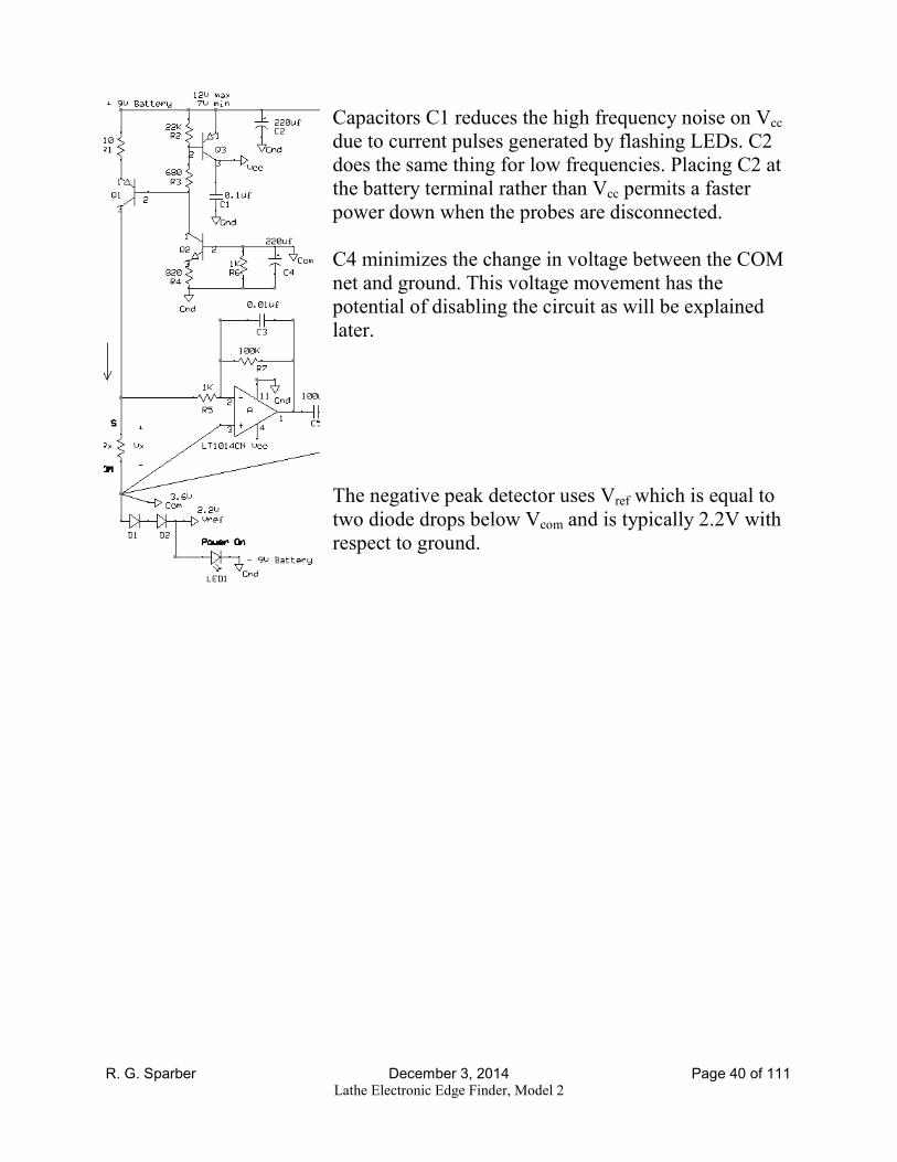
Capacitors C1 reduces the high frequency noise on Vcc
due to current pulses generated by flashing LEDs. C2
does the same thing for low frequencies. Placing C2 at
the battery terminal rather than Vcc permits a faster
power down when the probes are disconnected.
C4 minimizes the change in voltage between the COM
net and ground. This voltage movement has the
potential of disabling the circuit as will be explained
later.
The negative peak detector uses Vref which is equal to
two diode drops below Vcom and is typically 2.2V with
respect to ground.

R. G. Sparber December 3, 2014 Page 41 of 111 Lathe Electronic Edge Finder, Model 2
The First Gain Stage This is a simple inverting amplifier. The DC gain is set
by the ratio of R7 to R5 so comes out to
- X1X- = − 4..�4� = -100 (20)
Although R3 is rather small, it is much larger than any
reasonable Rx. So as far as input loading is concerned,
this gain stage has a very high input resistance.
The input bias current for this op amp is 30 nA
maximum. This current splits between R5 and R7. 4..4.4 × 30(� pass through R5
and 44.4 × 30(� passes through R7. This means that pin 2 is raised by 1� ×29.7(� = 29.7~�. The current through R7 is 0.3 nA so the voltage across R7
equals 0.3(� × 100� = 30~�.With pin 2 at 29.7 µV and R7 dropping 30µV,
the output is at -0.3 µV due to input bias current. It is therefore safe to ignore it.
Input offset voltage is another potential problem. It can be as high as ±0.3 mV.
That drives the output to as much as ±0.3�� × %−101& = ±30.3��. Good, not
a problem. [-108 mV with the probes tied together which implies a contact
resistance of between 4.q/�F:./�88.w/G×4.. = 34 milli ohms and
4.q/�c:./�88.w/G×4.. = 60 milli
ohms]
We cannot completely ignore the DC at the output of this gain stage. We must be
able to pass AC without distortion. So let's look at the maximum AC. This gain
stage multiplies the input by 100 and feeds it to the second gain stage which also
multiplies by 100. If the output of the second gain stage is at maximum, it can
output a signal centered around COM that is ± 1.3V. That means that the input to
this gain stage cannot be larger than ±4.:�4.. = 13�� which equals the output of the
first gain stage at pin 1 and is tiny.

R. G. Sparber December 3, 2014 Page 42 of 111 Lathe Electronic Edge Finder, Model 2
We do have a case where this first gain stage does
saturate. It occurs at large values of Rx. The
maximum �� is about 25 mA as found on page 6.
Note that the op amp is referenced to COM and not
ground. When the op amp is at negative saturation, it
is really hitting ground. So the maximum Vx with
respect to COM equals -3.6V. This means that �� �� = F�UVWF4.. (21)
��= F:.t�F4..
�� = 36��.
But �� =�� × �� %1& 36�� = �� × 25��
This gives us a maximum �� of :t/�8-/G = 1.4�ℎ��. As long as the contact
resistance between workpiece and cutter (in isolation) meets the spec of being no
larger than 0.6 ohms, there is no problem here. But if the parallel combination of
the spindle resistance and the contact resistance equaled more than 1.4 ohms, the
circuit would not be able to detect touchdown. The first gain stage would stay in
saturation. Of course, given resistances this big, a much simpler electronic edge
finder can be used7.
7 See http://rick.sparber.org/rctf.pdf .

R. G. Sparber December 3, 2014 Page 43 of 111 Lathe Electronic Edge Finder, Model 2
Update to First Stage
I have added a diode, D100 to the feedback loop. This
prevents op amp A from going more than 0.6V below
COM and prevents entering negative saturation. I have
found that once this op amp goes into saturation, it
disturbs node COM and upsets the rest of the circuit. It
also prevents the READY LED from flashing. At
touchdown, both the READY and Touchdown LEDs
flash but there is no indication that the circuit is
actually ready.
When V1 is at -0.6V, the voltage at the input is at F..t�F4.. = 6��.
First consider the case of no AC noise. Given a test current of 25 mA, this
translates into an �� of t/�8-/G = 0.24�ℎ��. So any �� greater than 0.24 ohms
looks to the circuit like it is 0.24 ohms as long as it is small enough to keep the
circuit powered up. The circuit should power up when an �� of up to 100 ohms is
connected.
We will consider the case of AC noise later because the negative peak detector is
the limiting factor here.
Note that if Rx is large enough, V1 will stay at about -0.6V even if some AC noise
is present. V1 will have very little AC in it.
So the addition of this feedback diode enables the circuit to work correctly with
spindle resistances between 0.01 ohms and 100 ohms.

R. G. Sparber December 3, 2014 Page 44 of 111 Lathe Electronic Edge Finder, Model 2
When we have �� large enough to cause the first gain stage to approach saturation,
we do run the risk of distorting an AC noise. However, the voltage transition at
touchdown is so large that the circuit can't miss it. So there really is no issue with
AC in this case.
The flip side to causing AC distortion is that AC cannot pass through the amplifier
if it is in saturation. With V1 sitting at a rail and dead quiet, the output of the
second gain stage, V7, will also be dead quiet. That means that the negative peak
detector will see a dead quiet signal.
We will later show that when the negative peak detector is in linear mode the
Ready LED does not flash. It will likely detect touchdown.

R. G. Sparber December 3, 2014 Page 45 of 111 Lathe Electronic Edge Finder, Model 2
My first line of defense against noise spikes
developed across Rx is C3. C3 in combination with
R7 gives me a low pass filter with a corner at 159 Hz.
I chose this corner frequency so it would attenuate
spikes a bit yet not blunt the step generated by
touchdown too much. As you can see, it has no effect
on 60 Hz noise.
Note the odd way I drew the connection from non-
inverting input of the op amp to my COM node. It is
essential that this be a direct connection with no other circuits sharing it. Any noise
injected into this input is multiplied by 10,000 by the time it gets to pin 7. If I had
0.3 micro volts of noise at pin 3 relative to COM it would become 3 millivolts of
noise at pin 7. That is 10% of my valid minimum signal. Additionally, the area
flanking this node should be ground to minimize capacitive coupling.

R. G. Sparber December 3, 2014 Page 46 of 111 Lathe Electronic Edge Finder, Model 2
The Second Gain Stage
Vx is multiplied by -100 as it appears at the
output of the first gain stage, pin 1. The
second gain stage is going to multiply it by
-100 again. This is only possible if I first
block any DC. Otherwise, I could only
tolerate about 30 mV at the output of the
first gain stage before I hit the rails at the
output of the second stage. My blocking
capacitor, C6, is a 100 µf ceramic capacitor
which has low leakage and no polarity.
My hat off to Mark Cason for finding this device for me.
I need as large a time constant as possible here so have set R8 equal to 10K. This
lets me pass the touchdown signal with minimal loss.
An R8 of 10K forces me to use a 1 Meg for R9 in order to get my gain of -100. I
will deal with the effect of input offset current and R9 later.
Capacitor C6 was chosen to have a time constant 10 times faster than the one in the
first gain stage. In this way it does not adversely affect the touchdown voltage
transition. Its main purpose is to block noise spikes that get into C5 and/or R8. A 1
milli volt spike at V7 can be generated by 10 micro volts of noise at the junction of
C5 and R8. I can't afford that.

R. G. Sparber December 3, 2014 Page 47 of 111 Lathe Electronic Edge Finder, Model 2
The Negative Peak Detector with Update
I'll admit it. This was the hardest part of
the design. It is a mix of analog and
digital which makes noise management
difficult. I need to be able to move a
central node in this circuit by many
volts quickly yet almost park it at any
point with fractions of a milli volt of
drift.
The circuit has two states. It is either
moving the voltage at pin 9, call it V9,
up or it is moving it down.
V9 moves up slowly. This movement is
defined by an exponential with a time
constant equal to R100 times C7.
When V9 is moving up, we can use a
simpler model to explain what is happening:
First, consider what v7(t) is doing. Assume it has a
large 60 Hz component and no DC offset. Given R100
= 4.7K and C7 = 100 uf, it can be shown that
�w%�& = −� 1��1�100 − � 1��1 × �1%0&���%��& � = 2�� = 377�����(�/�*��(�
�w%�& = −� 1377�100E�4.7� − � 1377�100E� × �1%0&���%��& Cosine is in radians.
�w%�& = −�26.54.7� − �26.8 ×�1%0&���%377�&

R. G. Sparber December 3, 2014 Page 48 of 111 Lathe Electronic Edge Finder, Model 2
�w%�& = F�8t.-0.1�F�8t.q × �1%0&���%377�&
�w%�& = 5.64 × 10F: × �1%0&���%377� − 1.57& (21.1)
Cosine is in radians.
Next, assume v7(t) is zero and look at how v9(t) moves from v9(0) towards zero.
Recall that v9(0) = v7(0). We have an RC circuit with the standard format of
�w%�& = �1%0&*��̀�� (21.2)
Where τ = R100 x C7.
This equation says that v9(t) starts out at the negative peak of v7 and discharges
towards zero.
Using Superposition, we can add (21.1) to (21.2) to get the total behavior at v9(t):
�w%�& = 5.64 × 10F: × �1%0&���%377� − 1.57&+�1%0&*��̀�� (21.3)
τ = R100 x C7 which nominally equals 0.47 seconds.
It will be later shown that we leave this simple model when t = 15.8 mS so
�w%�& = 5.64 × 10F: × �1%0&���%377�15.8�� − 1.57&+�1%0&*�4-.q/�F..01 � �w%�& = �1%0&%5.64 × 10F: × ���%377�15.8�� − 1.57& + *�4-.q/�F..01 �& �w%�& = �1%0&%−0.00181 + 0.967&
In other words, the AC component can be ignored. This was actually the intent of
connecting R100 to V7. I wanted to connect to COM but could not afford to pull
this much current out of the COM node. By connecting R100 to V7, I knew the AC
component would be blocked by C7 and I would be left with COM ± Vos of op
amp C.

R. G. Sparber December 3, 2014 Page 49 of 111 Lathe Electronic Edge Finder, Model 2
Of particular interest is how much �w rises during this 15.8 mS:
���*�(�w%�& = �1%0&%1 − 0.967& = 0.033 × �1%0& ���*�(�w%�&= 0.033 × �1%0& (21.4)
OK, let's test out
our new equation
using real data. My
bench model has a
R100 = 4.64K and
C7 = 69 uf. So RC
= 0.32. This means
that
���*�(�w%�&= 0.048 × �1%0& �1%0& equals (-4.5
divisions x 50
mV/division) = -
0.225V.
���*�(�w%�&= 0.048 × �1%0& ���*�(�w%�&= 0.048 × 0.225�
���*�(�w%�&= 11��
The picture shows a rise in �w%�& of 23 mV. So what is wrong here? If you look
closely at �w%�&, you will see that it changes on each cycle. This hints of noise. By
setting the scope to record the envelope of this signal, we see that it changes by 9.5
mVp-p. So a calculated rise of 11 mV might actually be as high as 20.5 mV. Recall
that �1%�& equals 10,000 times the input voltage so 9.5 mVp-p would take 0.95µV of
noise at the input. I realize this is not a very satisfying answer but after a few
weeks work, that is the best I got.
Next we will focus on how V9 moves down.

R. G. Sparber December 3, 2014 Page 50 of 111 Lathe Electronic Edge Finder, Model 2
V9 can move down very quickly. This is
accomplished by Q4.
V8 can either be at ground which is negative
saturation, or at a voltage more positive than Vref
which is about 2.2V as was shown back on page 32.
While V8 is at ground, Q4 is on. While V8 is above
Vref, Q4 is off.
When V10 is less than V9, V8 is at ground. Q4's
base is at about 2.2V so Q4 acts as a current source. The current equals
%����F���:&X48 =
%8.8�F..t-�&4q. = 8.6 mA. (22)
This current will flow as long as V9 is above Vref. Below
this voltage, Q4 is cut off. This also puts a limit on V7.
The best way to see this is to look at voltages with respect
to the COM node. Vref is 1.3V below this reference. So as
long as V7 is no more negative than -1.3V with respect to
COM, Q4 will operate correctly.
The top trace is V8.
Most of the time it is
at 2.8 divisions x
2V/div = 5.6V above
COM. To turn on
Q4, V8 dips below
about - 2V.
The bottom trace is
V9. It is at - 4.2 x
50mv = -219 mV
before V8 dips and -
4.6 x 50 mV = - 230
mV after V8 dips
low.
V9,
50
mV/
div
V8,
2V/
div
V8
V9

R. G. Sparber December 3, 2014 Page 51 of 111 Lathe Electronic Edge Finder, Model 2
In this example, V8
dips twice and you
can see how V9 steps
down twice.
Note that in both of
these examples, V8
did not reach down to
ground which is about
3.6V below COM.
The circuit was able
to get sufficient
current flow through
Q4 with less drive
voltage.

R. G. Sparber December 3, 2014 Page 52 of 111 Lathe Electronic Edge Finder, Model 2
When V8 is at ground, Q4 is full on and its
collector current is drawn from C7. We know that
��| = �1 L�yL# (23)
Plugging in what we know yields
8.6�� = 100μ� ×��w��
So L�yL# = 86 mV /ms.
Why do we care how fast we can pull V9? The answer is rather subtle. Consider
the case of detecting touchdown when a large AC voltage is present.

R. G. Sparber December 3, 2014 Page 53 of 111 Lathe Electronic Edge Finder, Model 2
First consider the steady state case of holding the
negative peak when a large AC signal is present.
Here we have V7 being applied to the negative
peak detector and V9 parked at its negative peak.
Since this is a 60 Hz signal, the period is 16.7 ms.
This means that every 16.7 ms, V9 is pulled down
to match the negative peak of V7. It is then free to
slowly rise for about 16.7 ms until it hits V7
coming down again. During that 16.7 ms, the
current flowing in R11 feeds into C7 and causes it to rise. Ignoring op amp C's bias
current plus any leakage currents in Q4 and Q5, this current is around w�F�UVWXee =w�F:.t�tq� = 79~�. Since V9 is going to be changing only a tiny amount compared
to the voltage across �44, we can treat this as a constant current and say that
�Xee = �1 L�yL# (24)
Plugging in what we know yields
79μ� = 100μ� × ��w16.7��
So ��w=1w�G×4t.1/v4..�� = 13��.
V9 will have drifted up 13 mV. This is a
rate of
L�yL# = dee�� = 1w�G4..�� = 0.79��/�� (25)
To recap, I can move V9 down at a rate of 86 mV/ms and it will drift up at a rate
over 100 times slower. This is the analog equivalent of digital memory.
R. G. Sparber December 3, 2014 Page 54 of 111 Lathe Electronic Edge Finder, Model 2
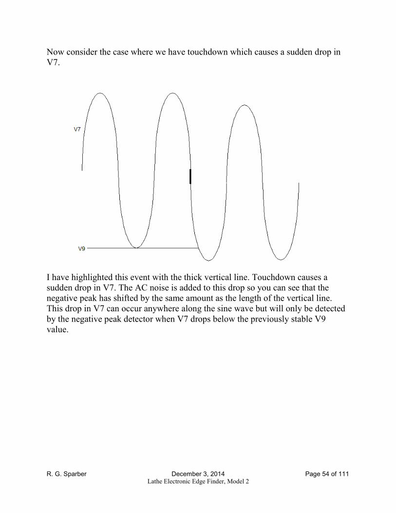
Now consider the case where we have touchdown which causes a sudden drop in
V7.
I have highlighted this event with the thick vertical line. Touchdown causes a
sudden drop in V7. The AC noise is added to this drop so you can see that the
negative peak has shifted by the same amount as the length of the vertical line.
This drop in V7 can occur anywhere along the sine wave but will only be detected
by the negative peak detector when V7 drops below the previously stable V9
value.
R. G. Sparber December 3, 2014 Page 55 of 111 Lathe Electronic Edge Finder, Model 2
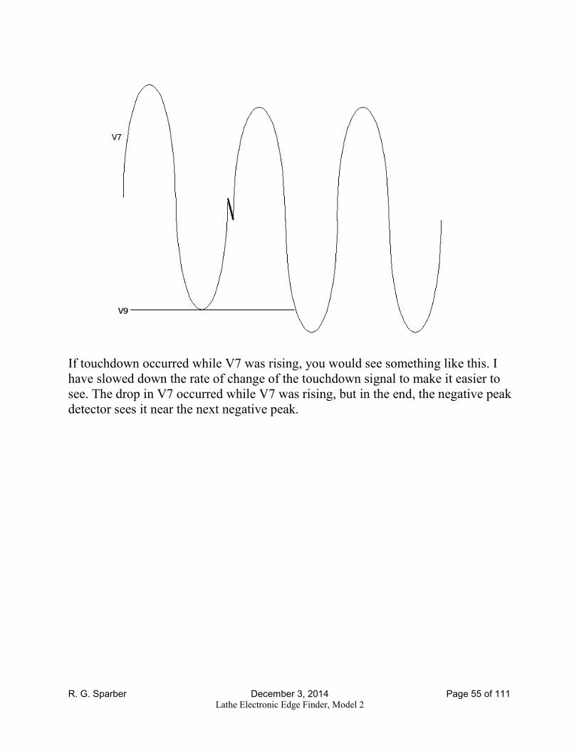
If touchdown occurred while V7 was rising, you would see something like this. I
have slowed down the rate of change of the touchdown signal to make it easier to
see. The drop in V7 occurred while V7 was rising, but in the end, the negative peak
detector sees it near the next negative peak.

R. G. Sparber December 3, 2014 Page 56 of 111 Lathe Electronic Edge Finder, Model 2
Now consider two cases.
In the first case, V9 moves down slowly relative to the rate of change of the AC
noise. It can only fall while V7 is less than V9. But before V9 can catch up, V7 has
turned around and headed back up again. On the next cycle, V9 again tries to reach
the negative peak but runs out of time. Eventually it will get there. But in the
meantime, the drop in V7 caused by touchdown is being divided into two or more
pieces. If it was small, then V9 might not drop enough at one time to trigger a
touchdown indication.
If the voltage drop due to touchdown is large, it might take a few cycles for V9 to
catch up to the negative peak of V7. This is harmless as long as the first drop is
large enough to detect.

R. G. Sparber December 3, 2014 Page 57 of 111 Lathe Electronic Edge Finder, Model 2
In the second case, V9 keeps
up with V7.
From page 16 we know that
the minimum drop in V7
that we must detect is 32.8
mV. For V9 not to miss any
of it, we must be able to
slew 32.8 mV.
From page 52 we found that
the slew rate for V9 is 86
mV /ms. So to move V9
32.8 mV
w0/�4/v = :8.q/��/v (26)
Solving for X we get
��� = :8.q/�qt/� × 1 ms = 0.381 ms (27)
So it will take Q4 0.381 ms to move V9 32.8 mV. This time interval is over at the
negative peak of V7.

R. G. Sparber December 3, 2014 Page 58 of 111 Lathe Electronic Edge Finder, Model 2
The 60 Hz noise signal can be described as
V7(t) = A sin(ωt)
where ω = 2πf
and the angle is in radians. (28)
The frequency is 60 Hz so 2π X 60 Hz = 377:
V7(t) = A sin(377t) (29)
The maximum value for A can be found from knowing that V7 cannot be lower
than Vref (see page 50). V7 swings symmetrically around the COM node which is
two diode drops above Vref. So our sine wave will swing down to Vref for its
maximum negative value. Therefore, we can set � = 2 ×�LO!L7 = 2 × 0.65� =1.3�.This gives us
V7(t) = 1.3 sin(377t) (30)
as our model for the maximum AC noise.

R. G. Sparber December 3, 2014 Page 59 of 111 Lathe Electronic Edge Finder, Model 2
Given the frequency is
60 Hz, we know that the
period is 4H = 16.667 ms.
The negative peak is ¾
the way through the
cycle so is at ¾ X 16.667
ms or 12.5 ms.
If we back up by 0.381 ms, we will be at the point of contact where V9 hits V7. So
that is at 12.5 ms - 0.381 ms = 12.12 ms. Plug that into the equation for V7(t) and
we get
V7(12.12 ms) = 1.3sin(377 x 12.12 ms) = -1.29V. Don't forget that this is in
radians and not degrees.
So V9 hits V7 when V7 is at -1.29V. In 0.381 ms, V7 is going to be at -1.3V. That
is a movement of -1.3V - {-1.29V} = -10mV in 0.381 ms or -26.2 mV/ms.
We have already figured out from page 52 that V9 can be made to fall at a rate of
86 mV/ms. Therefore, V9 can reach the negative peak in time. This does not
necessarily mean that V9 exactly follows V7.
Just for grins, let's see if V9 is fast enough to match the speed of V7.
We know from equation 30 that in the maximum case
V7(t) = 1.3sin(377t) (30)
The rate of change of V7(t) can be found by taking the derivative:
L�1L# = 1.3 × 377cos%377�& (31)
L�1L# = 490cos%377�& (32)
I have taken the derivative of the sin function and then used the chain rule on the
angle.
R. G. Sparber December 3, 2014 Page 60 of 111 Lathe Electronic Edge Finder, Model 2
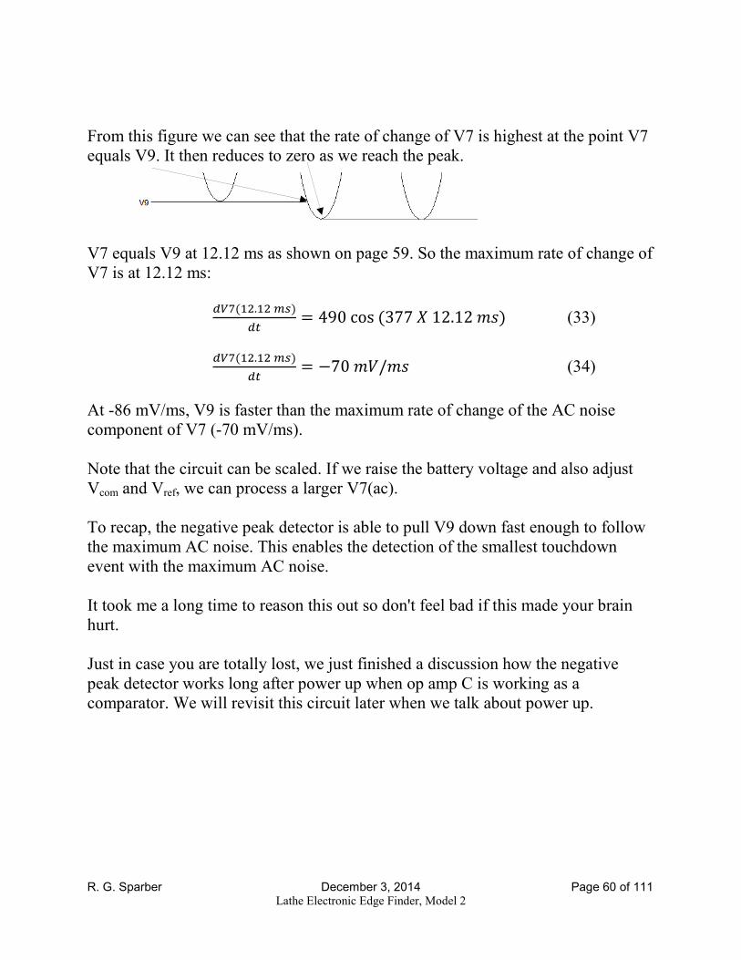
From this figure we can see that the rate of change of V7 is highest at the point V7
equals V9. It then reduces to zero as we reach the peak.
V7 equals V9 at 12.12 ms as shown on page 59. So the maximum rate of change of
V7 is at 12.12 ms:
L�1%48.48/v&L# = 490cos%377�12.12��& (33)
L�1%48.48/v&L# = −70��/�� (34)
At -86 mV/ms, V9 is faster than the maximum rate of change of the AC noise
component of V7 (-70 mV/ms).
Note that the circuit can be scaled. If we raise the battery voltage and also adjust
Vcom and Vref, we can process a larger V7(ac).
To recap, the negative peak detector is able to pull V9 down fast enough to follow
the maximum AC noise. This enables the detection of the smallest touchdown
event with the maximum AC noise.
It took me a long time to reason this out so don't feel bad if this made your brain
hurt.
Just in case you are totally lost, we just finished a discussion how the negative
peak detector works long after power up when op amp C is working as a
comparator. We will revisit this circuit later when we talk about power up.

R. G. Sparber December 3, 2014 Page 61 of 111 Lathe Electronic Edge Finder, Model 2
Consider the current path that quickly pulls V9
down. We know it flows through the collector of
Q4. From there, most of it flows out the emitter of
Q4, through R12, and into pin 8 of op amp C. The
output stage of the op amp conducts this current
into ground. The current is pulled out of ground
as it passes up into C7. Out the top of C7, we
finish the path as we reach the collector of Q4. In
this way the current path is fully defined,
minimized, and controlled.
This current is the single largest source of noise in the circuit. It is absolutely
essential that this current path avoid passing through any sensitive nodes. The most
sensitive node is COM. Noise on COM directly couples into the amplifiers. So
even though it would be nice to connect C9 to COM rather than ground, it injects
way too much noise. I will talk more about the COM node later.

R. G. Sparber December 3, 2014 Page 62 of 111 Lathe Electronic Edge Finder, Model 2
Now let's consider the special case where op
amp C acts in a linear fashion. V8 will sit at a
voltage close to Vref - Vbe4. The current flowing
in Q4's collector will be near the current
flowing in R11. A perfect balance will exist
where V9 will be constant and equal to V10
plus the input offset voltage of op amp C.
This case is only possible if V7 is dead quiet.
Any tiny drop in voltage will be quickly
followed by Q4 turning on. Any tiny rise will require time for R11 to pull V9 up.
Only when V7 is dead quiet can you sit in this linear mode.
As mentioned on page 43, if D100 is conducting, there is very little AC noise
present. The second voltage gain stage will then be very quiet too and V7 will be
dead quiet.

R. G. Sparber December 3, 2014 Page 63 of 111 Lathe Electronic Edge Finder, Model 2
The Ready LED Each time Q4 turns on, we also turn on LED2.
Random and short flashes of light from LED2 tell
us that the negative peak detector circuit is
regulating V9 and is therefore stable. That means
the circuit is ready to detect touchdown.
One thing that may surprise you is that V8
typically pulses low for just a few milliseconds.
The resulting flashes of light from the LED are
very brief yet easily seen.

R. G. Sparber December 3, 2014 Page 64 of 111 Lathe Electronic Edge Finder, Model 2
Blocking Capacitor, Comparator, and Touchdown LED
The voltage across C7 contains our touchdown event
but the pre-touchdown DC voltage is a function of
AC noise. We use C9 and R15 to remove this
unknown DC voltage. The time constant here is slow
enough to almost completely pass the touchdown
edge without attenuation. The voltage at pin 12 will
be near 0 with respect to the COM node before
touchdown and will drop by at least 32.8 mV at
touchdown. The larger the spindle resistance, the
larger the voltage drop at pin 12.
Notice that the change in voltage at pin 12 is coupled
through C9 and equals the change in voltage at the
top of C7. The bottom of C7 is connected to ground. So the change in voltage at
pin 12 is with respect to ground.
Now look at the voltage at pin 13. It comes from a voltage divider referenced to
COM. Any noise between ground and COM directly appears at the input of the
comparator. This may appear to be a design flaw but is actually a design
compromise.
As mentioned on page 61, I cannot allow current from Q4 to pass through the
COM node. So C7 must connect to ground. Yet I need V13 to be more negative
than V12 and there is no voltage more negative than ground. Furthermore, I must
permit V12 to dip below V13 as the touchdown occurs.
If I grounded V13 and put a positive DC bias in series with R19, I would get my
initial bias of 16.4 mV on V12 relative to V13. But when V9 dips low at
touchdown, V12 would also dip low and try to go below ground. This violates the
input requirements of the op amp. By referencing the COM node which is more
than 3V above ground, I have plenty of room for V12 to dip. By minimizing all
change in voltage between COM and ground, I was able to make this arrangement
work.

R. G. Sparber December 3, 2014 Page 65 of 111 Lathe Electronic Edge Finder, Model 2
If the input offset voltage is zero and there is no spike
noise, V13 is set to -16.4 mV. In practice, V13 is set
at a value that accommodates input offset voltage and
random voltage spikes in the shop. This is done by
watching the Touchdown LED and adjusting the
sensitivity until it does not flash in the idle state. Then
the cutter is fed in and the Touchdown LED should
flash at the moment of contact.
This is the moment of truth. If the random spike noise
in your shop is greater than the touchdown signal, it is
impossible for the circuit to tell them apart.
As long as V12 is lower than V13, the output, V14, will be near ground and LED3
will be lit. We will later talk about the time aspects of the circuit and you will see
that LED3 stays on for plenty of time to see it.
The input bias current is a maximum of 30 nA. This current flowing in R15
generates a maximum of �6OKv × �4- = 30(� × 470� = 14.1��[10��]. R19
exists to balance the bias current. In this way, the voltage at the wiper of R16 is
very close to the voltage on pin 12 with respect to pin 13.

R. G. Sparber December 3, 2014 Page 66 of 111 Lathe Electronic Edge Finder, Model 2
The COM Node
Let's follow where the COM node goes. Starting on the left, it is the reference node
for Vx. A single point has been defined as my COM node. Leading directly from
this point to pin 3 is my reference for the first gain stage. A second direct path
exists from this point to pin 5. It is the reference for the second gain stage. COM is
also connected to the touchdown LED's comparator. And lastly, COM connects to
the base of Q5.

R. G. Sparber December 3, 2014 Page 67 of 111 Lathe Electronic Edge Finder, Model 2
The voltage at pin 3 is extremely close to the voltage at the COM node. Any DC
difference is due to the input bias current flowing out of pin 3 and the resistance of
the path from pin 3 to the COM node. Any AC difference is due to noise pick up
which has been minimized by keeping the path short and having a ground plane
around it.
This enables the first gain stage to see almost entirely Vx with the least amount of
noise from the rest of the circuit. The output, V1, is with respect to pin 3 so
essentially with respect to COM. V1 is fed into our second gain stage which is also
directly connected to the COM node. This second gain stage sees V1 with respect
to pin 5 which is extremely close to the voltage at the COM node. Its output, V7, is
almost entirely a function of Vx and is referenced to pin 5 so essentially the voltage
a the COM node.
The key thing to remember here is that V7 is very quiet when measured with
respect to the COM node. I will emphasis this fact by taking about V7c, V7 with
respect to the COM node.
R. G. Sparber December 3, 2014 Page 68 of 111 Lathe Electronic Edge Finder, Model 2
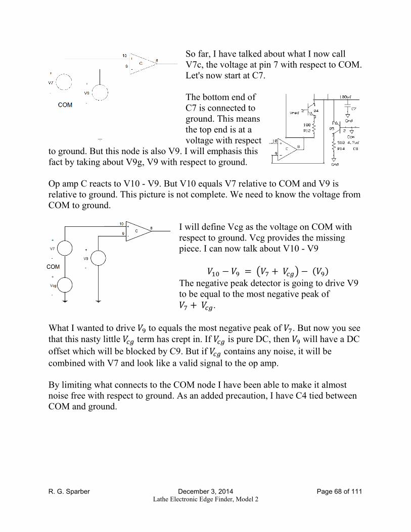
So far, I have talked about what I now call
V7c, the voltage at pin 7 with respect to COM.
Let's now start at C7.
The bottom end of
C7 is connected to
ground. This means
the top end is at a
voltage with respect
to ground. But this node is also V9. I will emphasis this
fact by taking about V9g, V9 with respect to ground.
Op amp C reacts to V10 - V9. But V10 equals V7 relative to COM and V9 is
relative to ground. This picture is not complete. We need to know the voltage from
COM to ground.
I will define Vcg as the voltage on COM with
respect to ground. Vcg provides the missing
piece. I can now talk about V10 - V9
�4. − �w = ¢�1 +�5£¤ −%�w& The negative peak detector is going to drive V9
to be equal to the most negative peak of �1 +�5£.
What I wanted to drive �w to equals the most negative peak of �1. But now you see
that this nasty little �5£ term has crept in. If �5£ is pure DC, then �w will have a DC
offset which will be blocked by C9. But if �5£ contains any noise, it will be
combined with V7 and look like a valid signal to the op amp.
By limiting what connects to the COM node I have been able to make it almost
noise free with respect to ground. As an added precaution, I have C4 tied between
COM and ground.
R. G. Sparber December 3, 2014 Page 69 of 111 Lathe Electronic Edge Finder, Model 2
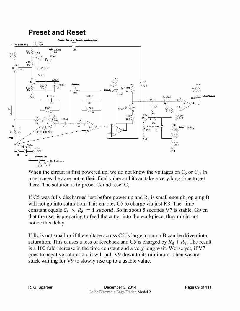
Preset and Reset
When the circuit is first powered up, we do not know the voltages on C5 or C7. In
most cases they are not at their final value and it can take a very long time to get
there. The solution is to preset C5 and reset C7.
If C5 was fully discharged just before power up and Rx is small enough, op amp B
will not go into saturation. This enables C5 to charge via just R8. The time
constant equals �- × �q = 1�*��(�. So in about 5 seconds V7 is stable. Given
that the user is preparing to feed the cutter into the workpiece, they might not
notice this delay.
If Rx is not small or if the voltage across C5 is large, op amp B can be driven into
saturation. This causes a loss of feedback and C5 is charged by �q + �w. The result
is a 100 fold increase in the time constant and a very long wait. Worse yet, if V7
goes to negative saturation, it will pull V9 down to its minimum. Then we are
stuck waiting for V9 to slowly rise up to a usable value.

R. G. Sparber December 3, 2014 Page 70 of 111 Lathe Electronic Edge Finder, Model 2
The solution is to add a Preset function. The user pushes the Preset button after
power first comes on. It quickly charges C5 to near the correct value and brings V7
to stability in a fraction of a second.
On the first pass of this explanation, I will assume an ideal op amp. Then I will add
in the critical parasitics.
Here is the second gain stage. For now, assume
that the output of the first gain stage has no AC
component. I will represent it as a DC voltage
source, V1. I don't know what the voltage is
across C5 so don't know the voltage V7. The
goal is to move V7 to zero and keep it there
when the Preset pushbutton is released.

R. G. Sparber December 3, 2014 Page 71 of 111 Lathe Electronic Edge Finder, Model 2
I push the Preset button. This connects the
junction of C5 and R8 to V7.
Let me redraw the circuit. I end up with R8 in
parallel with R9. C5 is tied to the output of the
op amp. I have not drawn C6 because it has no
effect here.

R. G. Sparber December 3, 2014 Page 72 of 111 Lathe Electronic Edge Finder, Model 2
Since no current can flow into the inputs of
this ideal op amp, I can simplify the circuit
further by replacing R8 and R9 with a short.
V7 of my ideal op amp is at zero volts because
that is the voltage at the positive input.
So the left end of C5 is at our unknown
voltage, V1, and the right end is at ground.
When the Preset button is released, we are
back to our origninal circuit but now the right
end of C5 has been charged to zero volts. V6
is also at zero volts due to feedback. This puts
zero volts across R8 so no current can flow in
it. This means that no current flows in R9 or
C6 either. Therefore, V7 is now at zero volts
too.
We started with C5 as some unknown voltage.
By pressing and releasing the Start button, V7
is quickly driven to zero volts.
The Preset works great given an ideal op amp. Too bad you can't buy an ideal op
amp.

R. G. Sparber December 3, 2014 Page 73 of 111 Lathe Electronic Edge Finder, Model 2
The op amp is not ideal. It has an input offset
voltage and an input bias current8. Let's consider
the input offset voltage first.
I will pull the input offset voltage, Vos, out of the
op amp so it is easier to see. V5 is now at a
voltage set by Vos. Due to the feedback, V6 is
very close toVos.
For the LT1014CN quad op amp, Vos worst case
is somewhere between -0.3 mV and +0.3 mV.
While the Preset button is pushed, we have this
circuit. V7 sits at Vos which is also the voltage at
the right end of C5.
I need to rely on one non-ideal feature of the op
amp for a moment. V7 acts as an ideal voltage
source until the output current reaches a limit.
Then it safely prevents more current to flow. I
rely on that feature to charge up C5 safely and
quickly.
When we release the Preset, the circuit reverts
back to its original configuration.
Notice that R8 has Vos on both ends. This means
that there is no voltage across it and therefore no
current through it. No current flowing in R8
means no current flowing through R9. So V7 is
equal to Vos. V7 was equal to Vos when the button
was being pushed, and it is still equal to Vos now
that it has been released.
8 It also has a gain less than infinite but that has little effect on the result in this case.
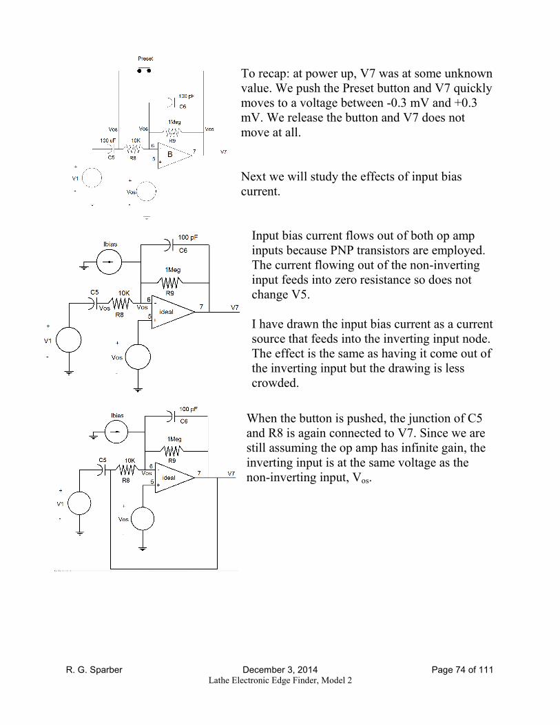
R. G. Sparber December 3, 2014 Page 74 of 111 Lathe Electronic Edge Finder, Model 2
To recap: at power up, V7 was at some unknown
value. We push the Preset button and V7 quickly
moves to a voltage between -0.3 mV and +0.3
mV. We release the button and V7 does not
move at all.
Next we will study the effects of input bias
current.
Input bias current flows out of both op amp
inputs because PNP transistors are employed.
The current flowing out of the non-inverting
input feeds into zero resistance so does not
change V5.
I have drawn the input bias current as a current
source that feeds into the inverting input node.
The effect is the same as having it come out of
the inverting input but the drawing is less
crowded.
When the button is pushed, the junction of C5
and R8 is again connected to V7. Since we are
still assuming the op amp has infinite gain, the
inverting input is at the same voltage as the
non-inverting input, Vos.

R. G. Sparber December 3, 2014 Page 75 of 111 Lathe Electronic Edge Finder, Model 2
Redrawing the circuit, we can see that the
input bias current all flows through R9 in
parallel with R10 which equals 9.9K. The
voltage across the equivalent resistance of
9.9K equals 9.9� �6OKv. The left end is
at Vos so
�1 = �!v −%9.9� ×�6OKv& (35)
This is also the voltage on the right end of
C5. Let me call it "Va".
Now the button is released. R8 has Vos
on the right end and at the instant the
button is released, Va on the left end still
equals �!v −%9.9� ×�6OKv& . The
initially current flowing through R8
towards C5 equals
�Xq = �!v −%�K&�8
�Xq = �!v −¢�!v −%9.9� ×�6OKv&¤�8
�Xq = ¢%9.9� ×�6OKv&¤�8
This current leaves the inverting input node. Entering this node is our input bias
current plus the current flowing through R9. So I can write
�Xq = �6OKv +�Xw
I can rearrange the terms and get
�Xw = �Xq −�6OKv

R. G. Sparber December 3, 2014 Page 76 of 111 Lathe Electronic Edge Finder, Model 2
�Xw = ¢%w.w�×f¥a{&¤Xq −�6OKv �Xw =¢%9.9� ×�6OKv&¤10� −�6OKv �Xw = %0.99 × �6OKv& −�6OKv �Xw =−0.01 × �6OKv
The minus sign says that the direction we
assumed for this current is backwards. The actual current flows towards V7. We
know the current through R9 and that the left end is tied to Vos. This lets us
calculate V7
�1 =�!v +%�w ×[−�Xw]& �1 =�!v +%�w ×[0.01 × �6OKv]&
Since this is at the instance the button is released, I will call this time t=0 and
rename V7 to V7(t). Then I can say
�1%0& = �!v +%�w ×[0.01 × �6OKv]&
The maximum Ibias is 30 nA for the LT1014CN. R9 = 1Meg. Vos can be as large as
0.3 mV. The most positive V7(0) is therefore
�1%0& = 0.3�� +%1¦*) ×[0.01 × 30(�]& �1%0& = 0.3�� +%0.3��& �1%0& = 0.6��

R. G. Sparber December 3, 2014 Page 77 of 111 Lathe Electronic Edge Finder, Model 2
The minimum Ibias is zero and Vos can be -0.3
mV. Therefore, the most negative V7(0) is
�1%0& = −0.3�� +%1¦*) ×[0.01 × 0]& �1%0& = −0.3��
We can therefore say that V7(0) is bounded by -0.3 mV and 0.6 mV.
Eventually C5 charges up and IR8 exponentially decays to zero. So after a "long"
time, I am left with
�6OKv =−�Xw
I can then write
�1%∞& = �!v −%�w ×�6OKv&
V7 starts at the voltage V7(0) and when it stops moving we are at V7(∞). The
change in voltage equals
�1%∞& −�1%0& = {�!v −%�w ×�6OKv&} − {¢�!v +%�w ×[0.01 × �6OKv]&¤} �1%∞& −�1%0& = −1.01 × %�w ×�6OKv&
Assuming the maximum Ibias of 30 nA and that R9 is 1 Meg, we get
�1%∞& −�1%0& = −1.01 × %1¦*) × 30(�& �1%∞& −�1%0& = −30.3��

R. G. Sparber December 3, 2014 Page 78 of 111 Lathe Electronic Edge Finder, Model 2
So V7 can fall by as much as 30.3
mV when the Preset button is
released. Note that this drop is
almost entirely a function of input
bias current and the 1 Meg resistor.
The input offset voltage canceled out
of the equation.
Since the op amp stays out of
saturation, the time constant is just �- × �q which is 100μ� × 10� = 1 second.
The negative peak detector will
follow V7 as long as it goes to a
lower value. If we get a
touchdown event while V7
decays, V9 will follow the
event. The slow decay of V7
has no effect9.
9 If V7(t) rose in voltage, we would be in trouble since V9 would ignore the rise. A
touchdown event would then have to cause V7 to drop below the previously lowest
value which would be V7(0).

R. G. Sparber December 3, 2014 Page 79 of 111 Lathe Electronic Edge Finder, Model 2
There is one case left to discuss. What if V1 is
not just a DC value? What if there is AC mixed
in?
First of all, consider the maximum AC value.
We know from page 58 that V7 can handle up
to 1.3Vpeak of AC. To get 1.3Vpeak out of this
gain stage means that we put in 4.:�¨�©ª4.. =13��«7KM. This would also be the voltage out
of the first gain stage, V1.
Now, think about what is going on when the
Preset button is being pushed. We are forcing
an AC voltage across C5. The impedance of
C5 at 60 Hz is −� 4¬� =−� 4:11×4..�� =−�26.5�ℎ��. In order to force 13 mVpeak
across it takes 4:/�8t.-!u/v = 0.49��. This is
well within the current sourcing and sinking
capabilities of the op amps.
At the instant the Preset button is released, V7 will be at zero. Then as V1
continues to move, the amplifier will multiply it by -100 and drive V7. In this way,
V7 will reflect just the AC component of V1 as it should.

R. G. Sparber December 3, 2014 Page 80 of 111 Lathe Electronic Edge Finder, Model 2
Now let's move on to the Reset for C7 which is part of the negative peak detector.
This is done before each touchdown.
There are two cases. In the first case V10 is higher than V9. This causes V8 to be
at positive saturation and Q4 to be off. R13 pulls up on V9 until Q5's emitter-base
junction is forward biased. Then V9 is clamped to about 0.65V above the COM
node. The current through R13 will be w�F�i®F�UVWX4: = w�F..t-�F:.t�X4: = 4.75��.
With a minimum =- of 80, the maximum current dumped into the COM node is 0.1-/Gq. = 59~�. This does disturb the voltage on COM relative to ground but no
touchdown event is being detected at this time so it is harmless.

R. G. Sparber December 3, 2014 Page 81 of 111 Lathe Electronic Edge Finder, Model 2
In the second case V10 is lower than V9. This causes op amp C to adjust V8 such
that V9 falls to match the negative peak of V10. The worst case is when V7 is 1.3V
below COM. This will cause op amp C to drive V8 to negative saturation which is
near 0 volts. That turns Q4 on to the maximum value. We then get a collector
current out of Q4 equal to �¯^°F�f^gX48 = 8.8�F..t-�4q.!u/v = 8.6��. The maximum current
flowing in R13 is when Q4 is just about to saturate. This means that V9 equals Vref. �X4: = w�F�¯^°X4: = w�F8.8�4� = 5.8��. This value is less than the maximum that can
be sunk by Q4 so Q4 will always win. V9 will always be pulled down to match the
negative peak of V7 when the Power On and Reset button is pushed.

R. G. Sparber December 3, 2014 Page 82 of 111 Lathe Electronic Edge Finder, Model 2
In this worst case, 8.6�� − 5.8�� = 2.8�� is
available to charge C7. As V9 rises, more current
will be available. The slowest V9 can move is
� = � L�L# (36)
2.8�� = 100μ� ��w��
��w�� = 2.8��100~�
So
��w�� = 28��/��
If I assume this slowest rate exists for the full range of V9 which is from 0.65V
above COM to 1.3V below COM, it will still take less than 4.:�c..t-�8q� = 80��to
move V9 into position. This is occurring while the button is being pushed. The
user will barely notice this delay.
Therefore, when the Power On and Reset button is released, the circuit will be
following V7. If V7 is stable, the circuit will be ready to detect touchdown.
If V7 is not stable, further time will be needed to establish the new negative peak.
The more noise mixed in with Vx, the more time it will take to stabilize.

R. G. Sparber December 3, 2014 Page 83 of 111 Lathe Electronic Edge Finder, Model 2
The Power On and Off Sequence
Back on page 31 I discussed most of the power control circuit.
To review, if Ix is flowing out of Q1, it flows mostly through our diode string
formed by D1, D2, and LED1 and through R6. That causes a voltage at the COM
node with respect to ground. This voltage is applied to the base of Q2 which causes
a collector current to flow. This collector current flows through R3, generates a
voltage, which is applied to R1 via Q1. The current through R1 is essentially Ix.
If Ix is not flowing, there is no voltage drop across our diode string, Q2 is off, and
no voltage can be developed across R3 or R1.
So we understand our ON state and our OFF state. How do we move between
them?

R. G. Sparber December 3, 2014 Page 84 of 111 Lathe Electronic Edge Finder, Model 2
The easy transition is from ON to OFF. By disconnecting one of the test probes, Ix
loses its path. This stops the current into our diode string and bleed resistor R6. C4
will hold up this voltage for short disruptions in Ix but then the COM node drops to
ground. That stops the current in Q2 so the voltage across R3 and R1 go to zero.
Moving from OFF to ON is not straight forward. If Vcom is greater than about
0.65V, Q2 will start to conduct. This will cause Ix to become non-zero and that, in
turn will cause Vcom to rise a bit more. This positive feedback will continue until
the diode string is stable. I just need to start the cycle and stand back.
So how do I pull up on the COM node without adding another pushbutton or a
second set of contacts on an existing pushbutton? This is where R14 comes in.
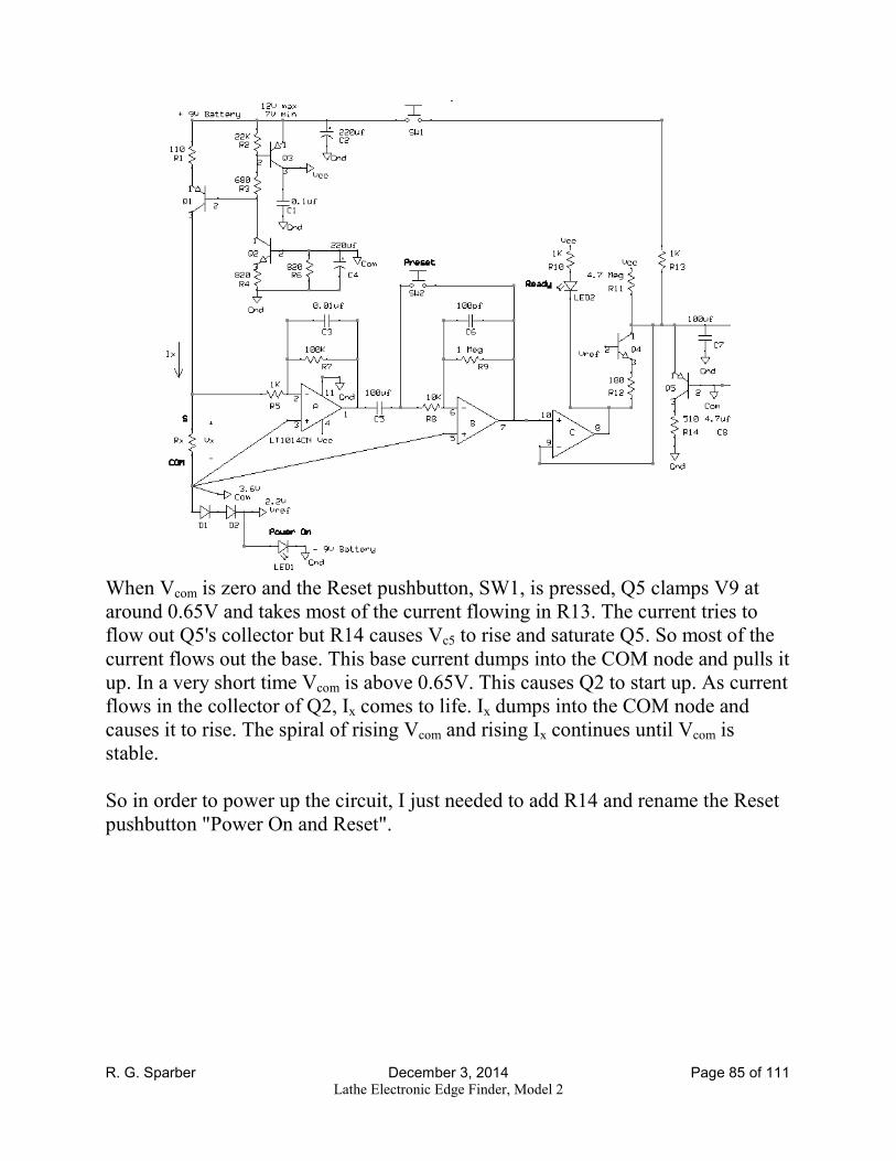
R. G. Sparber December 3, 2014 Page 85 of 111 Lathe Electronic Edge Finder, Model 2
When Vcom is zero and the Reset pushbutton, SW1, is pressed, Q5 clamps V9 at
around 0.65V and takes most of the current flowing in R13. The current tries to
flow out Q5's collector but R14 causes Vc5 to rise and saturate Q5. So most of the
current flows out the base. This base current dumps into the COM node and pulls it
up. In a very short time Vcom is above 0.65V. This causes Q2 to start up. As current
flows in the collector of Q2, Ix comes to life. Ix dumps into the COM node and
causes it to rise. The spiral of rising Vcom and rising Ix continues until Vcom is
stable.
So in order to power up the circuit, I just needed to add R14 and rename the Reset
pushbutton "Power On and Reset".

R. G. Sparber December 3, 2014 Page 86 of 111 Lathe Electronic Edge Finder, Model 2
The detailed analysis of this power up sequence takes many pages and has many
sub-state. I didn't think it was worth the time explaining it. However, it was fun to
do and does involve a negative resistor and an exponential that heads towards
infinity rather than an asymptote.
Shown above, in green, is the Power On and Reset button being pushed. The red
trace is Vcom rising from zero to its final value. The event takes less than 300 ms
and when done, the Power On LED turns on to confirm success.

R. G. Sparber December 3, 2014 Page 87 of 111 Lathe Electronic Edge Finder, Model 2
Time Constants
A detailed look at the time response of this circuit will be done with a simulator.
But to design the circuit, it is essential to reason it out.
When touchdown occurs, Vx will instantly drop a tiny amount. This will cause an
instant drop in the current through R5. That drop in current flows through C3 and
R7 to drive V1 to a smaller value. The time constant is �1 × �3 = 100� ×0.01~� = 1��.
V1 feeds into the second gain stage. It first sees C5 with its time constant of �5 × �8 = 100~� × 10� = 1�*��(�. So it will be invisible to the transition.
The next time constant involves C6 and R9. It yields 1¦*) × 100�� = 0.1��. Being ten times faster than the first gain stage, I can ignore it.
C7 really has no time constant since it moves as a function of V7 when V7 falls.

R. G. Sparber December 3, 2014 Page 88 of 111 Lathe Electronic Edge Finder, Model 2
The last time constant
involves C9 and R15. It is 0.47~� × 470� = 220
ms. Five of these time
constants equals 1.1
seconds.
When C7 is yanked up
during Reset, V12 rises
too. Assume V9 is held at
0.65V above COM for
more than 1.1 seconds.
Then C9 will charge up to
0.65V. This will put the left end of C9 at 0.65V and the right end at zero with
respect to COM.
Then when Q4 kicks in and pulls V9 down, V12 will fall and turn on the
Touchdown LED. After V9 is stable, it will take as much as 1.1 seconds for V12 to
return to zero and turn off the LED.

R. G. Sparber December 3, 2014 Page 89 of 111 Lathe Electronic Edge Finder, Model 2
When a touchdown event occurs, V1 will drop exponentially with a time constant
of around 1 ms due to the first gain stage. This transition will sail through the
second gain stage because C5 is so slow and C6 is so fast. The transition will
similarly pass through C9 because it is so slow. V12 will initially drop by the same
amount as seen on V7. After the initial transition, V9 will very slowly rise with a
time constant of �11 × �7 = 4.7¦*) × 100~� = 470�*��(��. C9 with R15
will see this slow rise as not moving and V12 will rise back to zero with its time
constant of 220 ms.
Note that I chose the time constant for C9 and R15 to be small so that I would not
have to build a reset circuit for it. The trade off is that the Touchdown LED does
not stay on for a "long" time. I do believe it is long enough to easily see. How long
it stays on depends on the magnitude of the drop at Vx. As long as V12 is less than
V13, the LED stays on.
The bottom line is that I have chosen time constants so each stage stays out of the
way of the rest. That sure simplifies hand analysis.

R. G. Sparber December 3, 2014 Page 90 of 111 Lathe Electronic Edge Finder, Model 2
Simulating the Circuit
I found it helpful to use a simulator, PSpice, to see what should be going on. It lets
me control every aspect of the circuit. Rather than use built in op amps, I formed
them from voltage controlled voltage sources to give me gain, Limit blocks to give
me my saturation voltages, DC supplies to give me input offset voltage, and DC
current sources to give me input bias. In the model shown here, I removed the
input offset voltage and input bias current sources that do not effect circuit
operation. R11 has not been updated for this section.
I did not simulate the difference between the COM node and ground. This study
was done on the bench with the real circuit.

R. G. Sparber December 3, 2014 Page 91 of 111 Lathe Electronic Edge Finder, Model 2
This is a trace of V7
during Preset. Power is
applied at time equal 0
and the Preset button is
pushed at 100 ms. It is
released at 500 ms.
You can see V7
quickly rise up to
almost 1.75V and
sit there while C5
starts to charge.
Then at 100 ms
the Preset starts
and V7 is moved
to near 0 in less
than 10 ms.
This is more of
the same trace. At
600 ms the Preset
button is released
and V7 falls to its
final value with a
time constant of 1
second. By 5 time
constants it is at
about -120 mV.
This voltage is
due to the input bias current of the second gain stage.

R. G. Sparber December 3, 2014 Page 92 of 111 Lathe Electronic Edge Finder, Model 2
This trace shows V9.
Recall that Preset, which
charges C5, started at 100
ms. The button was
released at 600 ms
although V7 was close to
its final value by 105 ms.
You can see V9 drop at
about 100 ms in response
to the drop in V7. V9 then
starts a slow rise until 1.0 seconds when the Reset button is pushed. This abruptly
pulls V9 up. It does not go all the way to 0.65V because Q4 is pulling it down. V9
follows the fall in V7 until the touchdown event at 5.0 seconds. It lasts until 7.0
seconds.
V9 drops by about 30 mV which is consistent with the discussion on page 13
related to minimum spindle resistance and maximum touchdown resistance. When
the touchdown event is over, V9 kicks up a little as C5 adjusts and then settles
back to its original value within a few seconds.
Reset
touchdown
Preset

R. G. Sparber December 3, 2014 Page 93 of 111 Lathe Electronic Edge Finder, Model 2
Now we are looking at V12.
The Preset of C5 at around
0.1 seconds caused V9 to
drop so you see this drop on
V12. Then we have the
Reset at 1.0 seconds which
causes a rise in V9. V9 has
settled out by 3.5 seconds.
Since the time constant of
C9 and R15 is much smaller than C7 and any of its time constants, V12 causes
little added delay before becoming stable. It is ready for the touchdown event at
5.0 seconds. You can see that the negative spike is almost 30 mV. We did blunt the
spike slightly by using the smaller C9/R15 time constant.

R. G. Sparber December 3, 2014 Page 94 of 111 Lathe Electronic Edge Finder, Model 2
Here is the final trace,
V14. When V14 is low,
the Touchdown LED is
on. We can see that the
Touchdown LED initially
is on when Preset is
taking place. The next
time it goes on is after
Touchdown. The
Touchdown LED is on for only 100 ms but this is plenty of time to see it.

R. G. Sparber December 3, 2014 Page 95 of 111 Lathe Electronic Edge Finder, Model 2
Scope Pictures
Test conditions:
Rx = 0.01 ohms
No induced AC noise.
The top trace is V7 at
20 mV/division. The
bottom trace is V9 at
20 mV/division. Time
base is 5 ms/division.
The "+" on the left side
indicates zero volts for
each trace.
You might be able to
see how V9 is
following the negative
peak of V7. When the
two traces share the
same zero volt line, it
is more obvious.

R. G. Sparber December 3, 2014 Page 96 of 111 Lathe Electronic Edge Finder, Model 2
Test conditions:
Rx = 0.01 ohms Rtouchdown = 0.6 ohms
Induced AC is above the maximum of 1.4V: 1.7V peak at V7
The green trace is V7 at 500 mV/division. The yellow trace is V14 at 5V/division.
Time base is 4 ms/division.
This is a touchdown event at above the maximum induced AC. You can see a
small drop in V7 just before V14 goes low. When V14 is low, the Touchdown LED
lights.
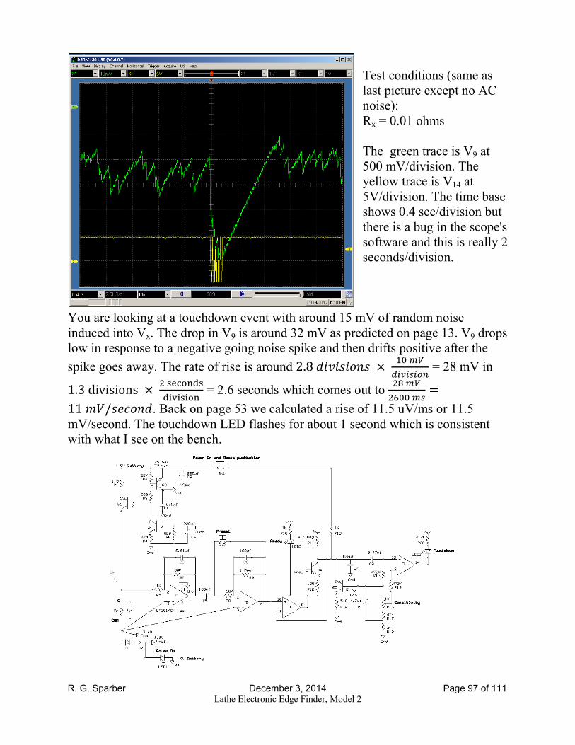
R. G. Sparber December 3, 2014 Page 97 of 111 Lathe Electronic Edge Finder, Model 2
Test conditions (same as
last picture except no AC
noise):
Rx = 0.01 ohms
The green trace is V9 at
500 mV/division. The
yellow trace is V14 at
5V/division. The time base
shows 0.4 sec/division but
there is a bug in the scope's
software and this is really 2
seconds/division.
You are looking at a touchdown event with around 15 mV of random noise
induced into Vx. The drop in V9 is around 32 mV as predicted on page 13. V9 drops
low in response to a negative going noise spike and then drifts positive after the
spike goes away. The rate of rise is around 2.8�������(� × 4./�LO�OvO!N = 28 mV in 1.3divisions ×8µ�¶·¸¹µ¹º»ºµº·¸ = 2.6 seconds which comes out to 8q/�8t../v =11��/�*��(�. Back on page 53 we calculated a rise of 11.5 uV/ms or 11.5
mV/second. The touchdown LED flashes for about 1 second which is consistent
with what I see on the bench.

R. G. Sparber December 3, 2014 Page 98 of 111 Lathe Electronic Edge Finder, Model 2
The rest of the scope
pictures were taken on
the prototype.
This scope picture is of
Vcom with respect to
ground. Below it is the
simulation. The final
value of Vcom is
different due to the
LED I am using in my
prototype but the wave
shapes are similar.
Vcom comes up in
about 160 ms in
this scope picture.
Vcom comes up in
about 170 ms in
the simulation.

R. G. Sparber December 3, 2014 Page 99 of 111 Lathe Electronic Edge Finder, Model 2
Here we have V7 with
respect to COM. The
vertical is 10 mV per
division. The horizontal is
40 ms per division. The
noise you see is mostly
picked up from Vx and not
internal to the circuit.
There are spikes in this
signal that are too fast to be
seen with a time base of 40
ms per division.

R. G. Sparber December 3, 2014 Page 100 of 111 Lathe Electronic Edge Finder, Model 2
This picture shows V9, in
green, and V8 in yellow. Both
are with respect to COM. When
V8 dips low, you see a sudden
drop in V9. The rest of the time
V9 is barely rising. The noise
you see on V9 is most likely
from the scope's power supply.
It is about 1 mV peak to peak.
This channel is set to 10 mV
per division. The time base is 2 ms per division.
The yellow trace is a lot quieter because the vertical is 5V per division.
R. G. Sparber December 3, 2014 Page 101 of 111 Lathe Electronic Edge Finder, Model 2
I am again looking at V9 and
V8 but this time you can see
multiple spike on V8 causing
V9 to step down to lower
values. The wider the spike,
the more V9 drops.
R. G. Sparber December 3, 2014 Page 102 of 111 Lathe Electronic Edge Finder, Model 2
This time I am looking at
V9 and V8 during a
touchdown event. You can
see V8 repeatedly pulling
down on V9 in order to
match the drop in V7. That
first flurry of spikes is
related to the actual
touchdown event. The rest
are probably reacting to
noise that has gotten into
the amplifier stages from V14 after touchdown.

R. G. Sparber December 3, 2014 Page 103 of 111 Lathe Electronic Edge Finder, Model 2
This scope picture is of V9
during a touchdown plus
V14. When V14 goes low,
the Touchdown LED goes on.
V14 went low after V9
dropped about 30 mV. The
subsequent drop is probably a
shift in COM with respect to
ground. It is harmless.

R. G. Sparber December 3, 2014 Page 104 of 111 Lathe Electronic Edge Finder, Model 2
This scope picture shows
V7 in green and V14 in
yellow. A 60 Hz noise
current has been induced
in the probes that
generated this 0.9V peak
signal. It translates to a
90 µV signal at Vx so is
30 times larger than the
touchdown event.

R. G. Sparber December 3, 2014 Page 105 of 111 Lathe Electronic Edge Finder, Model 2
Possible Future Improvements
Mark Cason has laid out a double sided and plans to sell both kits and finished
product.
I have very limited experience with this circuit in working machine shops. It works
fine in my shop and in two other shops.
The third shop is extremely noisy for two reasons. Plastic conduit was been used to
carry 220V so grounding is not as quiet plus radiation from the wires is not
enclosed as it would be with steel conduit. Secondly, a large CNC mill is present.
The voltage spikes from the table drive motors is large enough to cause false
touchdown indications.
One solution that does work is to raise the threshold voltage, V13, feeding the
touchdown LED comparator (op amp D). This reduces sensitivity to the
touchdown event and to the noise spike. In this case I am able to see the
touchdown event and ignore most of the voltage spikes. More testing is needed.

R. G. Sparber December 3, 2014 Page 106 of 111 Lathe Electronic Edge Finder, Model 2
Acknowledgements
I wish to thank Mark Cason for his hard work layout out the circuit many times.
Just when I thought I was done, something else caused a modification to be made.
His layout skills are truly amazing and it has been a pleasure working with him.
Thanks to Gregg C. for reviewing the circuit and suggesting key changes.
And a very special thanks to those people on various BBS that provided
inspiration.
These generous people again demonstrate that “all of us are smarter than any one
of us”.
I welcome your comments and questions.
Rick Sparber
Rick.Sparber.org

R. G. Sparber December 3, 2014 Page 107 of 111 Lathe Electronic Edge Finder, Model 2
Appendix: The LT1014 Op Amp
Here is a partial explanation of how the LT1014 op amp works.
V+ connects to Vcc which is around 9V. V
- connects to ground because it is the
most negative node in the circuit. Connected to the V- rail is Q24 which is on the
lower right side of the schematic.
Q24 is normally off. It only turns on when the output tries to sink more than about
22 mA. Q34 pulls down on the output node when current must be sunk by the op
amp. To do this, the voltage on the base of Q34 must rise. This is accomplished by
causing the base of Q31 to rise.
Now let's start at the input and work our way to Q31.The input PNPs, Q1 with Q27
and Q2 with Q28, form a differential circuit. Notice that the base of Q27 is
connected to the base of Q28. As the non-inverting input, IN+, falls relative to the
inverting input, IN-, it pulls down on the emitter of Q28. This causes an increase in
collector current flowing in Q28. This collector current is supplied by a current
source involving Q15. As Q28 takes more current, there is less current available

R. G. Sparber December 3, 2014 Page 108 of 111 Lathe Electronic Edge Finder, Model 2
for Q19. The result is a rise in voltage at the collector of Q19. The base of Q33 is
connected to this node. The rising of the base of Q33 causes the output node to
rise. That can cause an increase in current flowing out of the OUTPUT node. If
there is current flowing out of the OUTPUT node, then the voltage at the base of
Q33 with respect to the OUTPUT node increase. This causes the current in Q25's
collector to rise. More current in Q25's collector means more current flow in Q25's
emitter which means less current flowing in the emitter of Q32. We therefore get
less current flow in the collector of Q32. Less current flow in the collector of Q32
causes the base of Q31 to fall.

R. G. Sparber December 3, 2014 Page 109 of 111 Lathe Electronic Edge Finder, Model 2
As the base of Q31 falls, the collector current in Q34 falls. We therefore get an
increase in Q33's emitter current while we get a decrease in collector current in
Q34. Q33 and Q34 work in concert to increase the current flow out of the
OUTPUT node. It can be shown that if the current is flowing into the OUTPUT
node, the current through Q33 will fall and the current through Q34 will rise.
To sum up what we have found so far, as the IN+ voltage rises with respect to IN
-,
the OUTPUT node rises. Q33 works with Q34 to insure that the OUTPUT node
rises for both the case of current flowing into or out of this node.
Consider what happens if IN+ and IN
- rise the same amount. The base emitter
junction of Q28 does not change so the collector current does not change.
Therefore, the base of Q33 sees no change just as if IN+ and IN
- didn't move at all.
This is our Common Mode Rejection Ratio and is very large in this op amp.
Next we will look at power supply noise rejection. The top line is our V+
node. The
line parallel and just below it is our current source reference node. Q35 and
associated circuits control the voltage between V+ and this reference node. This
control is not a function of V+. The result is an array of current sources who's

R. G. Sparber December 3, 2014 Page 110 of 111 Lathe Electronic Edge Finder, Model 2
values are independent of V+. The op amp therefore achieves a high power supply
rejection ratio between V+ and the output. In other words, noise on V
+ relative to
ground is greatly attenuated before reaching the OUTPUT node.

R. G. Sparber December 3, 2014 Page 111 of 111 Lathe Electronic Edge Finder, Model 2
But what if the current is flowing into the OUTPUT node?
While IN+ falls, assume IN
- rises. This causes the base of Q1 to rise which cause
the emitter of Q27 to rise. But the base of Q27 is tied to the base of Q28. We know
that the base of Q28 is falling so with the emitter of Q27 rising, we get a reduction
in the current flowing in Q27.