Lecture Notes - SIETK ECEsietkece.com/wp-content/uploads/2016/08/DICA5.pdf · Lecture Notes Digital...
39
Transcript of Lecture Notes - SIETK ECEsietkece.com/wp-content/uploads/2016/08/DICA5.pdf · Lecture Notes Digital...

Lecture Notes Digital IC Applications
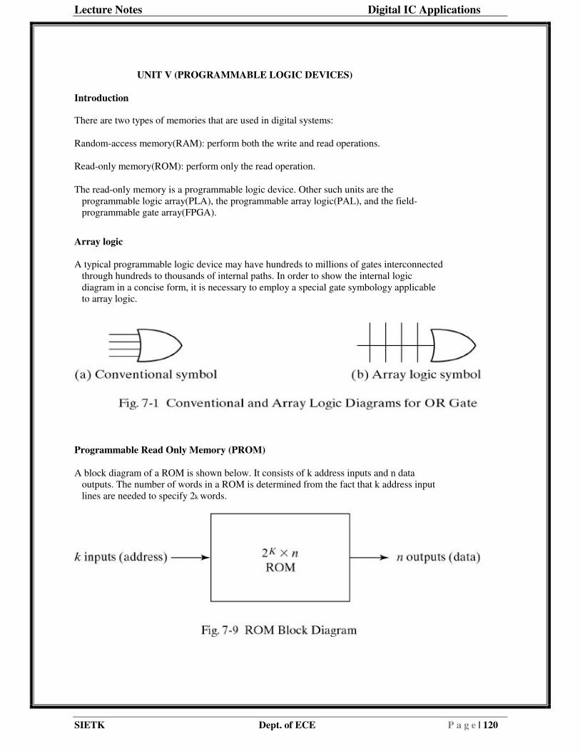
UNIT V (PROGRAMMABLE LOGIC DEVICES)
Introduction
There are two types of memories that are used in digital systems:
Random-access memory(RAM): perform both the write and read operations.
Read-only memory(ROM): perform only the read operation.
The read-only memory is a programmable logic device. Other such units are the programmable logic array(PLA), the programmable array logic(PAL), and the field- programmable gate array(FPGA).
Array logic
A typical programmable logic device may have hundreds to millions of gates interconnected through hundreds to thousands of internal paths. In order to show the internal logic diagram in a concise form, it is necessary to employ a special gate symbology applicable to array logic.
Programmable Read Only Memory (PROM)
A block diagram of a ROM is shown below. It consists of k address inputs and n data outputs. The number of words in a ROM is determined from the fact that k address input lines are needed to specify 2k words.
SIETK Dept. of ECE P a g e | 120

Lecture Notes
Digital IC Applications
Construction of ROM
Each output of the decoder represents a memory address. Each OR gate must be considered as having 32 inputs. A 2k X n ROM will have an internal k X 2k decoder and n OR gates.
Truth table of ROM
A programmable connection between to lines is logically equivalent to a switch that can be altered to either be close or open .Intersection between two lines is sometimes called a cross-point.
SIETK Dept. of ECE P a g e | 121

Lecture Notes Digital IC Applications
Programming the ROM
In Table 7-3, 0 � no connection
1 � connection
Address 3 = 10110010 is permanent storage using fuse link
Combinational circuit implementation
The internal operation of a ROM can be interpreted in two way: First, a memory unit that contains a fixed pattern of stored words. Second, implements a combinational circuit Fig. 7-11 may be considered as a combinational circuit with eight outputs, each being a function of the five input variables.
Example
Design a combinational circuit using a ROM. The circuit accepts a 3-bit number and generates an output binary number equal to the square of the input number.
SIETK Dept. of ECE P a g e | 122
Lecture Notes Digital IC Applications
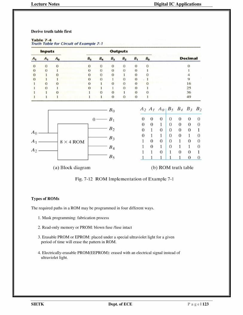
Derive truth table first
Types of ROMs
The required paths in a ROM may be programmed in four different ways.
1. Mask programming: fabrication process
2. Read-only memory or PROM: blown fuse /fuse intact
3. Erasable PROM or EPROM: placed under a special ultraviolet light for a given period of time will erase the pattern in ROM.
4. Electrically-erasable PROM(EEPROM): erased with an electrical signal instead of ultraviolet light.
SIETK Dept. of ECE P a g e | 123
Lecture Notes Digital IC Applications
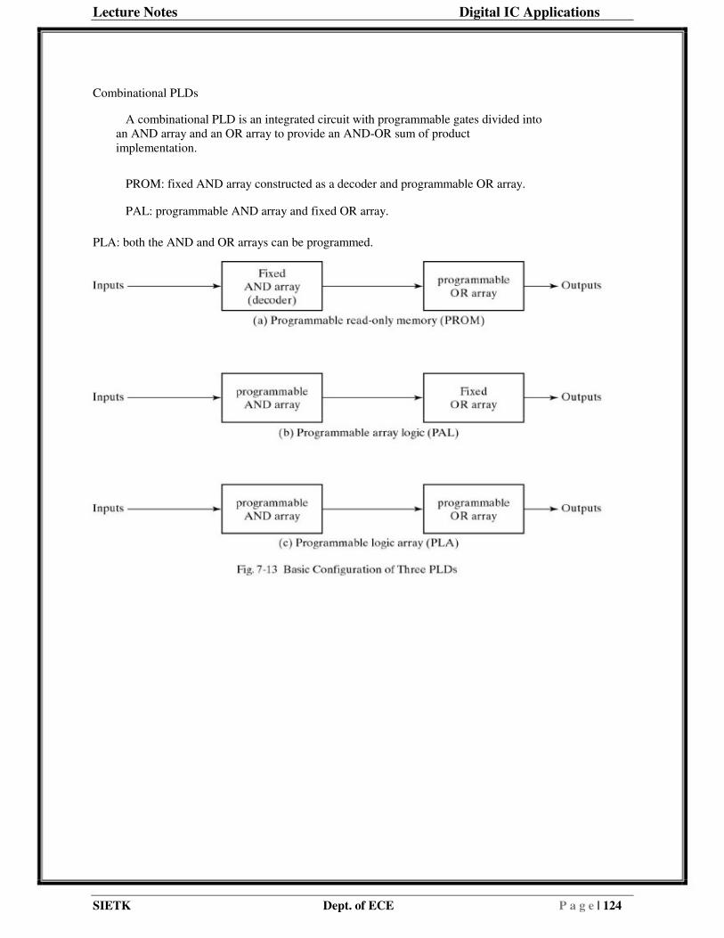
Combinational PLDs
� A combinational PLD is an integrated circuit with programmable gates divided into an AND array and an OR array to provide an AND-OR sum of product implementation.
� PROM: fixed AND array constructed as a decoder and programmable OR array.
� PAL: programmable AND array and fixed OR array.
PLA: both the AND and OR arrays can be programmed.
SIETK Dept. of ECE P a g e | 124
Lecture Notes Digital IC Applications
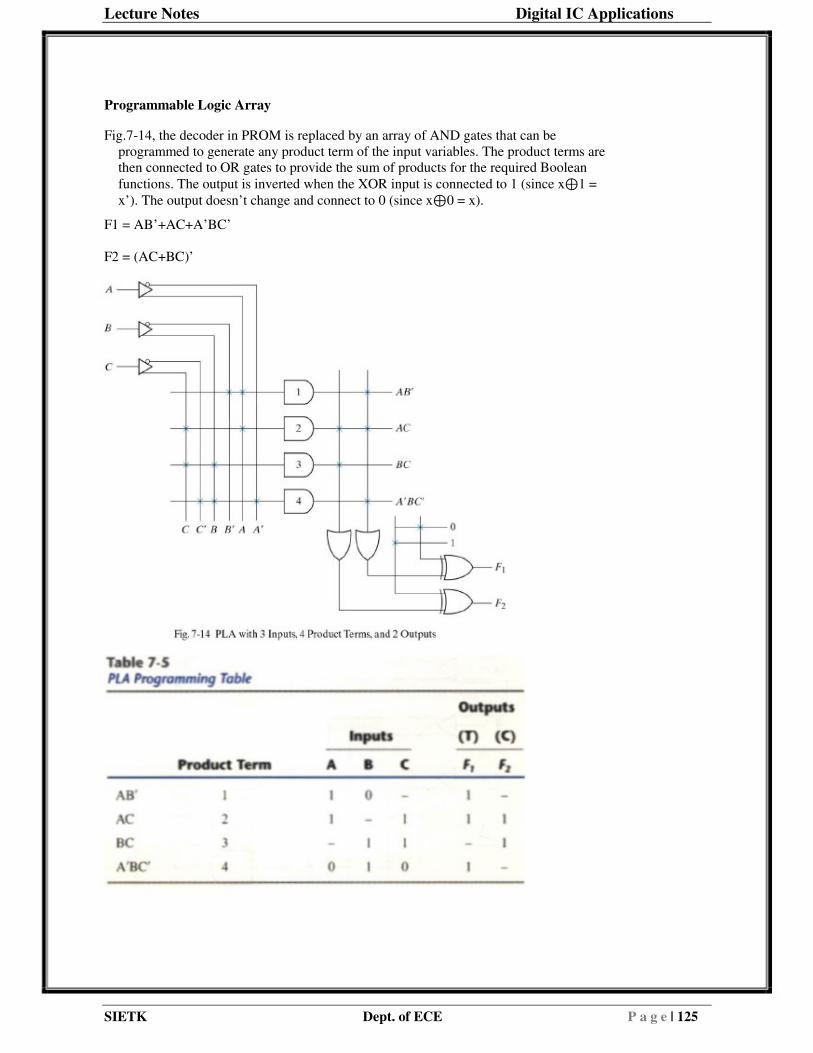
Programmable Logic Array
Fig.7-14, the decoder in PROM is replaced by an array of AND gates that can be programmed to generate any product term of the input variables. The product terms are then connected to OR gates to provide the sum of products for the required Boolean functions. The output is inverted when the XOR input is connected to 1 (since x⊕1 = x’). The output doesn’t change and connect to 0 (since x⊕0 = x).
F1 = AB’+AC+A’BC’
F2 = (AC+BC)’
SIETK Dept. of ECE P a g e | 125
Lecture Notes Digital IC Applications
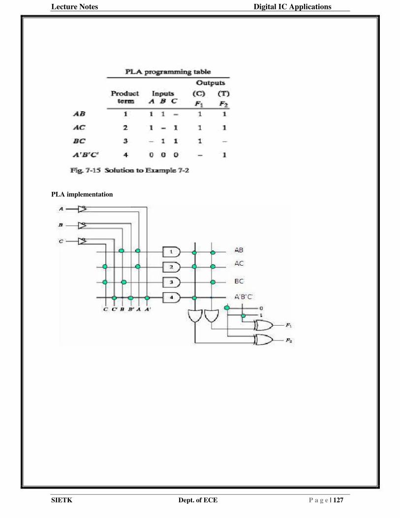
Programming Table
1. First: lists the product terms numerically
2. Second: specifies the required paths between inputs and AND gates
3. Third: specifies the paths between the AND and OR gates
4. For each output variable, we may have a T(ture) or C(complement) for programming the XOR gate
Simplification of PLA
Careful investigation must be undertaken in order to reduce the number of distinct product terms, PLA has a finite number of AND gates. Both the true and complement of each function should be simplified to see which one can be expressed with fewer product terms and which one provides product terms that are common to other functions.
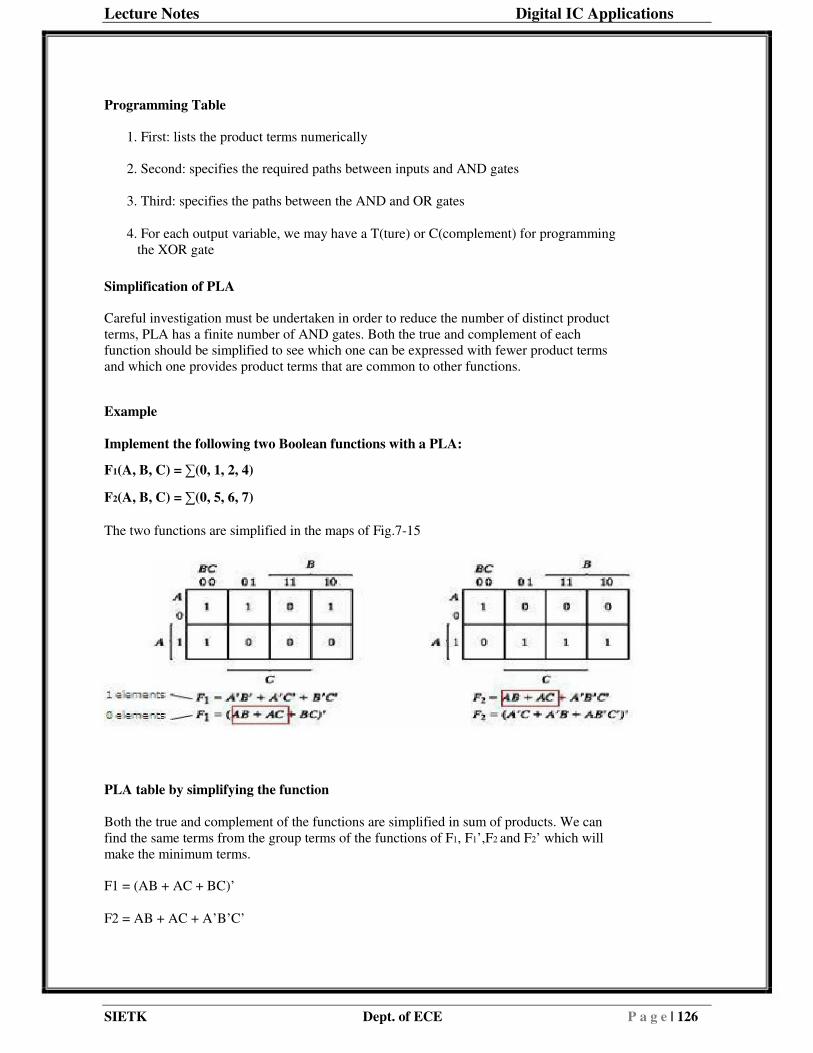
Example
Implement the following two Boolean functions with a PLA:
F1(A, B, C) = ∑(0, 1, 2, 4)
F2(A, B, C) = ∑(0, 5, 6, 7)
The two functions are simplified in the maps of Fig.7-15
PLA table by simplifying the function
Both the true and complement of the functions are simplified in sum of products. We can find the same terms from the group terms of the functions of F1, F1’,F2 and F2’ which will make the minimum terms.
F1 = (AB + AC + BC)’
F2 = AB + AC + A’B’C’
SIETK Dept. of ECE P a g e | 126
Lecture Notes Digital IC Applications
PLA implementation
SIETK Dept. of ECE P a g e | 127
Lecture Notes Digital IC Applications
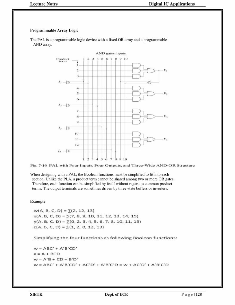
Programmable Array Logic
The PAL is a programmable logic device with a fixed OR array and a programmable AND array.
When designing with a PAL, the Boolean functions must be simplified to fit into each section. Unlike the PLA, a product term cannot be shared among two or more OR gates. Therefore, each function can be simplified by itself without regard to common product terms. The output terminals are sometimes driven by three-state buffers or inverters.
Example
SIETK Dept. of ECE P a g e | 128
Lecture Notes Digital IC Applications
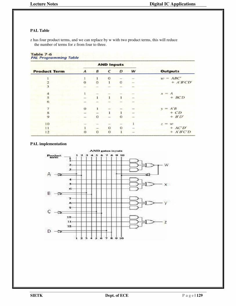
PAL Table
z has four product terms, and we can replace by w with two product terms, this will reduce the number of terms for z from four to three.
PAL implementation
SIETK Dept. of ECE P a g e | 129

Lecture Notes Digital IC Applications
Fuse map for example
Sequential Programmable Devices
Sequential programmable devices include both gates and flip-flops. There are several types of sequential programmable devices, but the internal logic of these devices is too complex to be shown here. We will describe three major types without going into their detailed construction.
1. Sequential (or simple) Programmable Logic Device (SPLD)
2. Complex Programmable Logic Device (CPLD)
3. Field Programmable Gate Array (FPGA)
SIETK Dept. of ECE P a g e | 130

Lecture Notes Digital IC Applications
FPLS
The first programmable device developed to support sequential circuit implementation is the field-programmable logic sequencer (FPLS).A typical FPLS is organized around a PLA with several outputs driving flip-flops. The flip-flops are flexible in that they can be programmed to operate as either JK or D type. The FPLS did not succeed commercially because it has too many programmable connections.
SPLD
Each section of an SPLD is called a macrocell. A macrocell is a circuit that contains a sum- of-products combinational logic function and an optional flip-flop. We will assume an AND- OR sum of products but in practice, it can be any one of the two-level implementation.
Macrocell
Fig.7-19 shows the logic of a basic macrocell. The AND-OR array is the same as in the combinational PAL shown in Fig.7-16.
CPLD
A typical SPLD has from 8 to 10 macrocells within one IC package. All the flip-flops are connected to the common CLK input and all three-state buffers are controlled by the EO input. The design of a digital system using PLD often requires the connection of several devices to produce the complete specification. For this type of application, it is more economical to use a complex programmable logic device (CPLD). A CPLD is a collection of individual PLDs on a single integrated circuit.
SIETK Dept. of ECE P a g e | 131

Lecture Notes Digital IC Applications
Fig.7-20 shows a general configuration of a CPLD. It consists of multiple PLDs interconnected through a programmable switch matrix. 8 to 16 macrocell per PLD.
Gate Array
The basic component used in VLSI design is the gate array. A gate array consists of a pattern of gates fabricated in an area of silicon that is repeated thousands of times until the entire chip is covered with the gates. Arrays of one thousand to hundred thousand gates are fabricated within a single IC chip depending on the technology used.
FPGA
FPGA is a VLSI circuit that can be programmed in the user’s location. A typical FPGA logic block consists of look-up tables, multiplexers, gates, and flip-flops. Look-up table is a truth table stored in a SRAM and provides the combinational circuit functions for the logic block.
Differential of RAM and ROM in FPGA
The advantage of using RAM instead of ROM to store the truth table is that the table can be programmed by writing into memory.
The disadvantage is that the memory is volatile and presents the need for the look-up table content to be reloaded in the event that power is disrupted.
SIETK Dept. of ECE P a g e | 132

Lecture Notes Digital IC Applications
Comparison between PROM, PLA and PAL
SIETK Dept. of ECE P a g e | 133

Lecture Notes Digital IC Applications
UNIT V
ROMs
SIETK Dept. of ECE P a g e | 134

Lecture Notes Digital IC Applications
UNIT V (MEMORIES)
Introduction
There are two types of memories that are used in digital systems:
Random-access memory (RAM): perform both the write and read operations.
Read-only memory (ROM): perform only the read operation.
The read-only memory is a programmable logic device. Other such units are the programmable logic array (PLA), the programmable array logic (PAL), and the field- programmable gate array (FPGA).
Random-Access Memory
A memory unit stores binary information in groups of bits called words.
1 byte = 8 bits
1 word = 2 bytes
The communication between a memory and its environment is achieved through data input and output lines, address selection lines, and control lines that specify the direction of transfer.
Content of a memory
Each word in memory is assigned an identification number, called an address, starting from 0 up to 2k-1, where k is the number of address lines. The number of words in a memory with one of the letters K=210, M=220, or G=230.
64K = 216 2M = 221 4G = 232
SIETK Dept. of ECE P a g e | 135

Lecture Notes Digital IC Applications
Write and Read operations
Transferring a new word to be stored into memory:
1. Apply the binary address of the desired word to the address lines.
2. Apply the data bits that must be stored in memory to the data input lines.
3. Activate the write input.
Transferring a stored word out of memory:
1. Apply the binary address of the desired word to the address lines.
2. Activate the read input.
SIETK Dept. of ECE P a g e | 136

Lecture Notes Digital IC Applications
Commercial memory sometimes provide the two control inputs for reading and writing in a somewhat different configuration in table 7-1.
Timing Waveforms (write)
The access time and cycle time of the memory must be within a time equal to a fixed number of CPU clock cycles. The memory enable and the read/write signals must be activated after the signals in the address lines are stable to avoid destroying data in other memory words. Enable and read/write signals must stay active for at least 50ns.
SIETK Dept. of ECE P a g e | 137

Lecture Notes Digital IC Applications
Timing Waveforms (read)
The CPU can transfer the data into one of its internal registers during the negative transition of T3.
Types of memories
In random-access memory, the word locations may be thought of as being separated in space, with each word occupying one particular location. In sequential-access memory, the information stored in some medium is not immediately accessible, but is available only certain intervals of time. A magnetic disk or tape unit is of this type. In a random-access memory, the access time is always the same regardless of the particular location of the word. In a sequential-access memory, the time it takes to access a word depends on the position of the word with respect to the reading head position; therefore, the access time is variable.
Static RAM
SRAM consists essentially of internal latches that store the binary information. The stored information remains valid as long as power is applied to the unit. SRAM is easier to use and has shorter read and write cycles. Low density, low capacity, high cost, high speed, high power consumption.
Dynamic RAM
DRAM stores the binary information in the form of electric charges on capacitors. The capacitors are provided inside the chip by MOS transistors. The capacitors tend to discharge with time and must be periodically recharged by refreshing the dynamic memory. DRAM
SIETK Dept. of ECE P a g e | 138

Lecture Notes Digital IC Applications
offers reduced power consumption and larger storage capacity in a single memory chip. High density, high capacity, low cost, low speed, low power consumption. Types of memories
Memory units that lose stored information when power is turned off are said to be volatile. Both static and dynamic, are of this category since the binary cells need external power to maintain the stored information. Nonvolatile memory, such as magnetic disk, ROM, retains its stored information after removal of power.
Memory decoding
The equivalent logic of a binary cell that stores one bit of information is shown below.
Read/Write = 0, select = 1, input data to S-R latch
Read/Write = 1, select = 1, output data from S-R latch
*Refer SR latch with NOR gates
4X4 RAM
There is a need for decoding circuits to select the memory word specified by the input address. During the read operation, the four bits of the selected word go through OR gates to the output terminals. During the write operation, the data available in the input lines are transferred into the four binary cells of the selected word. A memory with 2k words of n bits per word requires k address lines that go into kx2k decoder
SIETK Dept. of ECE P a g e | 139

Lecture Notes Digital IC Applications
Coincident decoding
A decoder with k inputs and 2k outputs requires 2k AND gates with k inputs per gate. Two decoding in a two-dimensional selection scheme can reduce the number of inputs per gate. 1K-word memory, instead of using a single 10X1024 decoder, we use two 5X32 decoders.
SIETK Dept. of ECE P a g e | 140
Lecture Notes Digital IC Applications
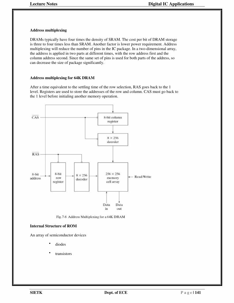
Address multiplexing
DRAMs typically have four times the density of SRAM. The cost per bit of DRAM storage is three to four times less than SRAM. Another factor is lower power requirement. Address multiplexing will reduce the number of pins in the IC package. In a two-dimensional array, the address is applied in two parts at different times, with the row address first and the column address second. Since the same set of pins is used for both parts of the address, so can decrease the size of package significantly.
Address multiplexing for 64K DRAM
After a time equivalent to the settling time of the row selection, RAS goes back to the 1 level. Registers are used to store the addresses of the row and column. CAS must go back to the 1 level before initialing another memory operation.
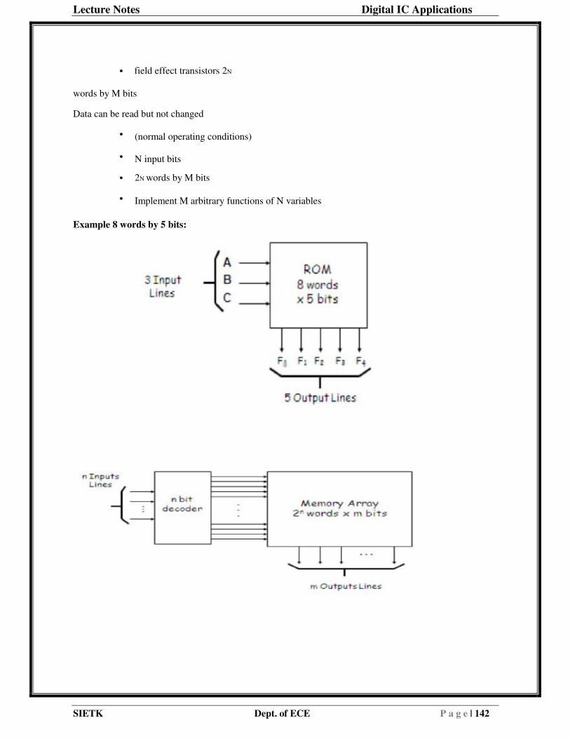
Internal Structure of ROM
An array of semiconductor devices
•
•
diodes
transistors
SIETK Dept. of ECE P a g e | 141
Lecture Notes Digital IC Applications
• field effect transistors 2N
words by M bits
Data can be read but not changed
•
•
•
•
(normal operating conditions)
N input bits
2N words by M bits
Implement M arbitrary functions of N variables
Example 8 words by 5 bits:
SIETK Dept. of ECE P a g e | 142

Lecture Notes Digital IC Applications
ROM Memory Array
Alternate view
Each possible horizontal/vertical intersection indicates a possible connection. Or gates at bottom output the word selected by the decoder (32 x 8)
SIETK Dept. of ECE P a g e | 143

Lecture Notes Digital IC Applications
Commercial ROM types
EPROM
Uses a floating gate for the FET at each bit location. User uses a programming voltage that causes a temporary breakdown in the dielectric between the gate and the floating gate to charge it. When programming voltage is removed the charge stays. How long? EPROM manufacturers ―guaranteeǁ properly programmed bit has 70% of charge after 10 years. Use UV light to erase.
SIETK Dept. of ECE P a g e | 144

Lecture Notes Digital IC Applications
EEPROM
Electrically Erasable PROM. Like the EPROM only electrically erasable in circuit. Many times referred to a ―flashǁ programmable memory. Very slow on writes so not a substitute for RAM.
General Block Diagram of ROM
Timing Diagram of ROM
SIETK Dept. of ECE P a g e | 145
Lecture Notes Digital IC Applications
•
• •
•
•
Access time from address – tAA
Access time from chip select - tACS Output-enable time - tOE
Output-disable time - tOZ
Output-hold time - tOH
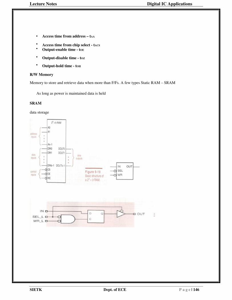
R/W Memory
Memory to store and retrieve data when more than F/Fs. A few types Static RAM – SRAM
As long as power is maintained data is held
SRAM
data storage
SIETK Dept. of ECE P a g e | 146
Lecture Notes Digital IC Applications
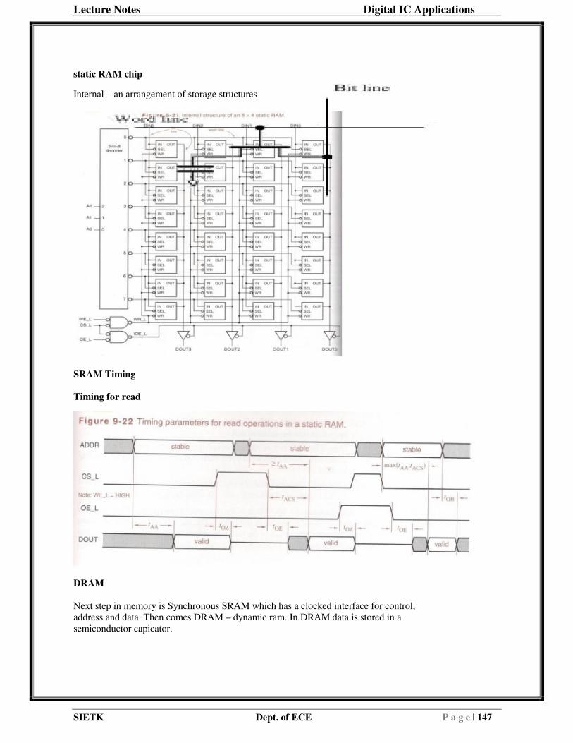
static RAM chip
Internal – an arrangement of storage structures
SRAM Timing
Timing for read
DRAM
Next step in memory is Synchronous SRAM which has a clocked interface for control, address and data. Then comes DRAM – dynamic ram. In DRAM data is stored in a semiconductor capicator.
SIETK Dept. of ECE P a g e | 147

Lecture Notes Digital IC Applications
DRAM Read
A read sees the bit line precharged to high. The word line is then activated. If cell stores a 0 then there is a small drop on the voltage on the bit line. This is monitored by a sense amp which provides the value stored. Value must be written back after the read.
DRAM Refresh
Charge stored leaks off over time. Must restore the values stored a 4096 row DRAM it
refresh every 64ms and thus each row every 15.6 usec. Larger DRAMs are banks of smaller.
DDR SDRAM
Double data rate SDRAM. Double the data transfer rate of an SDRAM by transferring on both edges of the clock. Access and setup times are the same as SRAM. Increased data throughput as data is transferred in blocks.
DRAM structure and operation
Write operation
Setting the word line to 1.To store a 1, a HIGH voltage is placed on the bit line, which charges the capacitor through the ―onǁ transistor. To store a 0, a LOW voltage is placed on the bit line, which discharges the capacitor through the ―onǁ transistor.
Read operation
The bit line is first precharged to a voltage halfway between HIGH and LOW. The word line is set HIGH so that the precharged bit line is pulled slightly higher or slightly lower. A sense amplifier detects this small change and recovers a 1 or 0 accordingly. Reading a DRAM cell destroy the original voltage stored on the capacitor, the DRAM cell must be written back the original data after reading.
Internal structure of a 64Kx1 DRAM
Multiplexed address inputs.
SIETK Dept. of ECE P a g e | 148

Lecture Notes Digital IC Applications
RAS_L: Row address strobe to store the higher order bits of the address into the row-address register.
CAS_L: Column address strobe to store the lower order bits of the address into the column- address register.
Row latches: the latches used to store data input/output from the memory array.
RAM Cells
Static RAM (SRAM):
•
•
•
•
The basic element of a static RAM cell is the D-Latch.
Data remains stored in the cell until it is intentionally modified.
SRAM is fast (Access time: 1ns).
SRAM needs more space on the semiconductor chip than DRAM.
– SRAM more expensive than DRAM
– SRAM needs more space than DRAM
•
•
SRAM consumes power only when accessed.
SRAM is used as a Cache
Dynamic RAM (DRAM):
•
•
•
•
DRAM stores data in the form of electric charges in capacitors.
Charges leak out, thus need to refresh data every few ms.
DRAM is slow (Access time: 60ns).
DRAM needs less space on the semiconductor chip than SRAM. – DRAM less expensive than SRAM
– DRAM needs less space than SRAM
•
•
DRAM needs to be refreshed
DRAM is used as the main memory
Types of semiconductor memory devices: Static RAM
Static RAM (also called SRAM)devices retain their data for as long as the DC power is applied. The most common family of SRAM are the 61XXX, 62XXX or the CMOS
SIETK Dept. of ECE P a g e | 149

Lecture Notes Digital IC Applications
62CXXX series, where XXX indicates the memory capacity in Kbits. Some members of this family are the following:
6116/6216(2Kx8)
61256/62256(32Kx8)
6164/6264 (8Kx8)
611024/621024 (128Kx8)
These series of SRAM devices are pin compatible with the 27XXX series of EPROMs, with the difference that the WR signal is replaced by the programming voltage pin (Vpp) on the EPROM. This allows a single socket on the PCB hold either a SRAM, during system development, or an EPROM, after the operation of the program is verified to be the expected one. Static RAM is fast with access times much less than 100ns. SRAM chips with access times less than 10ns are often used as cache memory in computers.
DYNAMIC RAM CELL ARRAY
Asynchronous DRAM
This is the basic form, from which all others are derived. An asynchronous DRAM chip has power connections, some number of address inputs (typically 12), and a few (typically 1 or 4) bidirectional data lines. There are four active low control signals: /RAS, the Row Address Strobe. The address inputs are captured on the falling edge of /RAS, and select a row to open. The row is held open as long as /RAS is low. /CAS, the Column Address Strobe. The address inputs are captured on the falling edge of /CAS, and select a column from the currently open row to read or write. /WE, Write Enable. This signal determines whether a given falling edge of /CAS is a read (if high) or write (if low). If low, the data inputs are also captured on the falling edge of /CAS. /OE, Output Enable. This is an additional signal that controls output to the data I/O pins. The data pins are driven by the DRAM chip if /RAS and /CAS are low, and /WE is high, and /OE is low. In many applications, /OE can be permanently connected low (output always enabled), but it can be useful when connecting multiple memory chips in parallel.
SIETK Dept. of ECE P a g e | 150

Lecture Notes Digital IC Applications
DYNAMIC RAM
DRAM requires refreshing every 2 to 4 ms . Refreshing
occurs automatically during a read or write.
Internal circuitry takes care of refreshing cells that are not accessed over this interval.
– For a 256K X 1 DRAM with 256 rows, a refresh must occur every 15.6us (4ms/256).
SIETK Dept. of ECE P a g e | 151

Lecture Notes Digital IC Applications
– For the 8086, a read or write occurs every 800ns .
– This allows 19 memory reads/writes per refresh or 5% of the time. DRAM technologies
– EDO DRAM
– SDRAM
– DRDRAM
– DDR DRAM
Soft errors occur on DRAMs which often require ERROR DETECTION and/or ERROR CORRECTION
A DRAM CONTROLLER is required for using DRAM
SYNCHRONOUS DYNAMIC RAM
In a synchronous DRAM, the control signals are synchronized with the system bus clock and therefore with the microprocessor. It allows pipelined read/write operations
Double Data Rate (DDR) DRAM
An SDRAM type of memory where data are transferred on both the rising and the falling clock edge, effectively doubling the transfer rate without increasing the clock frequency.DDR-200 means a transfer rate of 200 million transfers per second, at a clock rate of 100 MHz.DDR1 upto 400 MHz.DDR2 standard allows higher clock frequencies.
DRAM
Refresh circuit : storage decay in ms
DRAMs take up much less space, typically ¼ the silicon area of SRAMs or less (one transistor and a capacitor)
SIETK Dept. of ECE P a g e | 152

Lecture Notes Digital IC Applications
DRAM Organization
Long rows to simplify refresh. Two new signals: RAS, CAS. Row Address Strobe, Column Address Strobe replace Chip Select.
RAS, CAS Addressing
Even to read 1 bit, an entire 64-bit row is read! Separate addressing into two cycles: Row Address, Column Address. Saves on package pins, speeds RAM access for sequential bits!
SIETK Dept. of ECE P a g e | 153
Lecture Notes Digital IC Applications
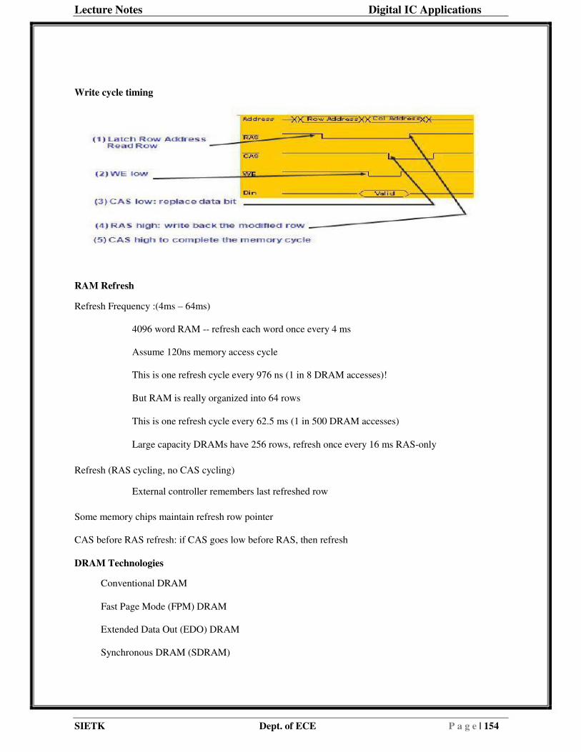
Write cycle timing
RAM Refresh
Refresh Frequency :(4ms – 64ms)
� 4096 word RAM -- refresh each word once every 4 ms
� Assume 120ns memory access cycle
� This is one refresh cycle every 976 ns (1 in 8 DRAM accesses)!
� But RAM is really organized into 64 rows
� This is one refresh cycle every 62.5 ms (1 in 500 DRAM accesses)
� Large capacity DRAMs have 256 rows, refresh once every 16 ms RAS-only
Refresh (RAS cycling, no CAS cycling)
� External controller remembers last refreshed row
Some memory chips maintain refresh row pointer
CAS before RAS refresh: if CAS goes low before RAS, then refresh
DRAM Technologies
� Conventional DRAM
� Fast Page Mode (FPM) DRAM
� Extended Data Out (EDO) DRAM
� Synchronous DRAM (SDRAM)
SIETK Dept. of ECE P a g e | 154

Lecture Notes Digital IC Applications
� Double Data Rate SDRAM (DDR SDRAM)
� Direct Rambus DRAM (DRDRAM)
� Synchronous-Link DRAM (SLDRAM)
Fast Page Mode (FPM) DRAM
Sending the row address just once for many accesses to memory in locations near each other, improving access time
� Page
Burst mode access
� Memory is not read one byte at a time (32 or 64 bits at a time)
� Several consecutive chunks of memory
� ―x-y-y-yǁ for four consecutive accesses
mode
SIETK Dept. of ECE P a g e | 155

Lecture Notes Digital IC Applications
Synchronous DRAM
Tied to the system clock
Burst mode
� System timing : 5-1-1-1
� Internal interleaving New memory
standard for modern PCs Speed
� Access time: 10ns, 12ns,…
� MHz rating: 100 MHz, 133MHz
Latency
� SDRAMs are still DRAMs
� 5-1-1-1 (10ns means the second, third and fourth access times) 2-clock and 4-
clock Circuitry
� 2-clock: 2 different DRAM chips on the module
SIETK Dept. of ECE P a g e | 156
Lecture Notes Digital IC Applications
��4-clock: 4 different DRAM chips
Packaging
� Usually comes in DIMM packaging
� Buffered and unbuffered, 3.3 V and 5.0V
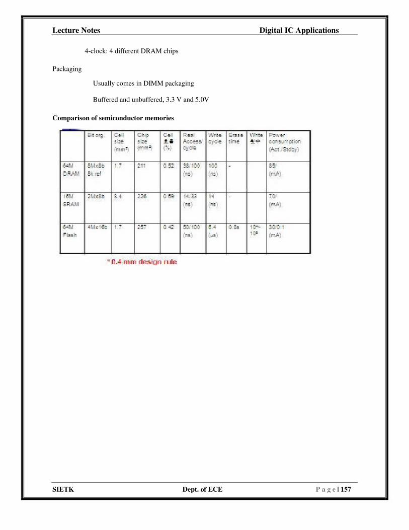
Comparison of semiconductor memories
SIETK Dept. of ECE P a g e | 157


![vlsi & embedded systems lab - SIETK ECE DEPARTMENT · 2018. 7. 16. · SIETK, ECE [VLSI & EMBEDDED SYSTEMS LAB] 2 (15A04712) VLSI & EMBEDDED SYSTEMS LABORATORY Note: The students](https://static.fdocuments.us/doc/165x107/60a68df82b16b22c09239fcb/vlsi-embedded-systems-lab-sietk-ece-department-2018-7-16-sietk-ece.jpg)


![UNIT –I NETWORK TOPOLOGY - SIETK College · NETWORK TOPOLOGY 1. A tree has ... 23. The cutset schedule gives relation between [ ] A) Branch currents and link currents B) branch](https://static.fdocuments.us/doc/165x107/5adb6ccc7f8b9a6d7e8df226/unit-i-network-topology-sietk-topology-1-a-tree-has-23-the-cutset-schedule.jpg)