Lecture Notes on Power Electronics - Pick My...
75
(6TH SEMESTER) POWER ELECTRONICS (3-1-0) MODULE-I (10 HOURS) Thyristors, Static V-I Characteristics of SCR, TRIAC, GTO & IGBT, Turn-On & Turn-OFF Mechanism of SCR, Gate Turnoff Thyristor (GTO) .Power BJTs . Power MOSFETs - Insulated Gate Bipolar Transistors (IGBTs) - Basic Structure and VI Characteristics. Static, dynamic and thermal characteristics. Protection, cooling and mounting techniques. Series and Parallel operation of devices. Triggering and basics of driver circuits. Different types of commutation schemes: Natural and Forced commutation. MODULE-II (10 HOURS) 1-Phase Half & Full Wave Controlled Rectifier with various kinds of loads (R, R-L-E (motor)). Midpoint and Bridge type converters. Half Controlled and Fully Controlled Bridge circuits, different waveforms, Input Line Current Harmonics, Power factor, current distortion and displacement factors- Inverter Mode of Operation. Continuous and discontinuous modes, Effect of source inductance assuming constant load current. Effect of freewheeling diode. Three phase bridge converters for different types of load with constant load current, different waveforms. 180 and 120 degree operations. MODULE-III (10 HOURS) DC-DC Converters: Classification of types of choppers, One, Two and Four quadrant operations, Step up and down choppers, Analysis of Type-A chopper, Single-and two quadrant operation with DC motor load. AC-AC Converters: Single-phase mid-point and bridge types of step-up and step-down Cycloconverters. Single phase AC Voltage regulators and its basic analysis. MODULE-IV (10 HOURS) Single-phase Half and Full bridge Inverter, Pulse Width Modulated (PWM) technique for voltage control, SPWM Technique 1-phase inverters, Auxiliary Commutated (Mc-Murray) and Complementary Commutated (Mc-Murray Bedford) Inverters, Three-phase Voltage Source Bridge type of Inverters. (120 and 180 Degree conduction modes), Current Source Inverter. Applications: UPS, SMPS, Induction Heating, Electronic Ballast, AC/DC drives speed control. Get Discount Coupons for your Coaching Institute and FREE Study Material at www.PickMyCoaching.com Get Discount Coupons for your Coaching Institute and FREE Study Material at www.PickMyCoaching.com www.PickMyCoaching.com
-
Upload
truongmien -
Category
Documents
-
view
215 -
download
1
Transcript of Lecture Notes on Power Electronics - Pick My...

(6TH SEMESTER)
POWER ELECTRONICS (3-1-0)
MODULE-I (10 HOURS)
Thyristors, Static V-I Characteristics of SCR, TRIAC, GTO & IGBT, Turn-On & Turn-OFF Mechanism of SCR, Gate Turnoff Thyristor (GTO) .Power BJTs . Power MOSFETs - Insulated Gate Bipolar Transistors (IGBTs) - Basic Structure and VI Characteristics. Static, dynamic and thermal characteristics. Protection, cooling and mounting techniques. Series and Parallel operation of devices. Triggering and basics of driver circuits. Different types of commutation schemes: Natural and Forced commutation. MODULE-II (10 HOURS)
1-Phase Half & Full Wave Controlled Rectifier with various kinds of loads (R, R-L-E (motor)). Midpoint and Bridge type converters. Half Controlled and Fully Controlled Bridge circuits, different waveforms, Input Line Current Harmonics, Power factor, current distortion and displacement factors- Inverter Mode of Operation. Continuous and discontinuous modes, Effect of source inductance assuming constant load current. Effect of freewheeling diode. Three phase bridge converters for different types of load with constant load current, different waveforms. 180 and 120 degree operations. MODULE-III (10 HOURS)
DC-DC Converters: Classification of types of choppers, One, Two and Four quadrant operations, Step up and down choppers, Analysis of Type-A chopper, Single-and two quadrant operation with DC motor load. AC-AC Converters: Single-phase mid-point and bridge types of step-up and step-down Cycloconverters. Single phase AC Voltage regulators and its basic analysis. MODULE-IV (10 HOURS)
Single-phase Half and Full bridge Inverter, Pulse Width Modulated (PWM) technique for voltage control, SPWM Technique 1-phase inverters, Auxiliary Commutated (Mc-Murray) and Complementary Commutated (Mc-Murray Bedford) Inverters, Three-phase Voltage Source Bridge type of Inverters. (120 and 180 Degree conduction modes), Current Source Inverter. Applications: UPS, SMPS, Induction Heating, Electronic Ballast, AC/DC drives speed control.
Get Discount Coupons for your Coaching Institute and FREE Study Material at www.PickMyCoaching.com
Get Discount Coupons for your Coaching Institute and FREE Study Material at www.PickMyCoaching.com
www.Pick
MyCoa
ching
.com

MODULE - 1
Get Discount Coupons for your Coaching Institute and FREE Study Material at www.PickMyCoaching.com
Get Discount Coupons for your Coaching Institute and FREE Study Material at www.PickMyCoaching.com
www.Pick
MyCoa
ching
.com

POWER ELECTRONICS
The control of electric motor drives requires control of electric power. Power electronics have eased the concept of power control. Power electronics signifies the word power electronics and control or we can say the electronic that deal with power equipment for power control.
Main power source
Ref signal
Power electronics based on the switching of power semiconductor devices. With the development of power semiconductor technology, the power handling capabilities and switching speed of power devices have been improved tremendously.
Power Semiconductor Devices
The first SCR was developed in late 1957. Power semiconductor devices are broadly categorized into 3 types:
1. Power diodes (600V,4500A) 2. Transistors 3. Thyristors (10KV,300A,30MW)
Thyristor is a four layer three junction pnpn semiconductor switching device. It has 3 terminals these are anode, cathode and gate. SCRs are solid state device, so they are compact, possess high reliability and have low loss.
Control
Circuit
Digital
Circuit
Power
Electronic
circuit
Load
Feedback Signal
Get Discount Coupons for your Coaching Institute and FREE Study Material at www.PickMyCoaching.com
Get Discount Coupons for your Coaching Institute and FREE Study Material at www.PickMyCoaching.com
www.Pick
MyCoa
ching
.com

SCR is made up of silicon, it act as a rectifier; it has very low resistance in the forward direction and high resistance in the reverse direction. It is a unidirectional device.
Static V-I characteristics of a Thyristor
The circuit diagram for obtaining static V-I characteristics is as shown
Anode and cathode are connected to main source voltage through the load. The gate and cathode are fed from source 𝐸𝑆.
A typical SCR V-I characteristic is as shown below:
Get Discount Coupons for your Coaching Institute and FREE Study Material at www.PickMyCoaching.com
Get Discount Coupons for your Coaching Institute and FREE Study Material at www.PickMyCoaching.com
www.Pick
MyCoa
ching
.com

𝑉𝐵𝑂=Forward breakover voltage
𝑉𝐵𝑅=Reverse breakover voltage
𝐼𝑔=Gate current
𝑉𝑎=Anode voltage across the thyristor terminal A,K.
𝐼𝑎=Anode current
It can be inferred from the static V-I characteristic of SCR. SCR have 3 modes of operation:
1. Reverse blocking mode 2. Forward blocking mode ( off state) 3. Forward conduction mode (on state)
1. Reverse Blocking Mode
When cathode of the thyristor is made positive with respect to anode with switch open thyristor is reverse biased. Junctions 𝐽1 and 𝐽2 are reverse biased where junction 𝐽2 is forward biased. The device behaves as if two diodes are connected in series with reverse voltage applied across them.
A small leakage current of the order of few mA only flows. As the thyristor is reverse biased and in blocking mode. It is called as acting in reverse blocking mode of operation.
Now if the reverse voltage is increased, at a critical breakdown level called reverse breakdown voltage 𝑉𝐵𝑅,an avalanche occurs at 𝐽1 and 𝐽3 and the reverse
Get Discount Coupons for your Coaching Institute and FREE Study Material at www.PickMyCoaching.com
Get Discount Coupons for your Coaching Institute and FREE Study Material at www.PickMyCoaching.com
www.Pick
MyCoa
ching
.com

current increases rapidly. As a large current associated with 𝑉𝐵𝑅 and hence more losses to the SCR.
This results in Thyristor damage as junction temperature may exceed its maximum temperature rise.
2. Forward Blocking Mode
When anode is positive with respect to cathode, with gate circuit open, thyristor is said to be forward biased.
Thus junction 𝐽1 and 𝐽3 are forward biased and 𝐽2 is reverse biased. As the forward voltage is increases junction 𝐽2 will have an avalanche breakdown at a voltage called forward breakover voltage𝑉𝐵𝑂. When forward voltage is less then 𝑉𝐵𝑂thyristor offers high impedance. Thus a thyristor acts as an open switch in forward blocking mode.
3. Forward Conduction Mode
Here thyristor conducts current from anode to cathode with a very small voltage drop across it. So a thyristor can be brought from forward blocking mode to forward conducting mode:
1. By exceeding the forward breakover voltage. 2. By applying a gate pulse between gate and cathode.
During forward conduction mode of operation thyristor is in on state and behave like a close switch. Voltage drop is of the order of 1 to 2mV. This small voltage drop is due to ohmic drop across the four layers of the device.
Different turn ON methods for SCR
1. Forward voltage triggering 2. Gate triggering 3. 𝑑𝑣
𝑑𝑡 triggering
4. Light triggering 5. Temperature triggering
1. Forward voltage triggering
Get Discount Coupons for your Coaching Institute and FREE Study Material at www.PickMyCoaching.com
Get Discount Coupons for your Coaching Institute and FREE Study Material at www.PickMyCoaching.com
www.Pick
MyCoa
ching
.com
A forward voltage is applied between anode and cathode with gate circuit open.
Junction 𝐽1 and 𝐽3 is forward biased. Juntion 𝐽2 is reverse biased. As the anode to cathode voltage is increased breakdown of the reverse biased junction
𝐽2 occurs. This is known as avalanche breakdown and the voltage at which this phenomena occurs is called forward breakover voltage.
The conduction of current continues even if the anode cathode voltage reduces below 𝑉𝐵𝑂till 𝐼𝑎 will not go below𝐼ℎ. Where 𝐼ℎ is the holding current for the thyristor.
2. Gate triggering
This is the simplest, reliable and efficient method of firing the forward biased SCRs. First SCR is forward biased. Then a positive gate voltage is applied between gate and cathode. In practice the transition from OFF state to ON state by exceeding 𝑉𝐵𝑂 is never employed as it may destroy the device. The magnitude of 𝑉𝐵𝑂, so forward breakover voltage is taken as final voltage rating of the device during the design of SCR application.
First step is to choose a thyristor with forward breakover voltage (say 800V) higher than the normal working voltage. The benefit is that the thyristor will be in blocking state with normal working voltage applied across the anode and cathode with gate open. When we require the turning ON of a SCR a positive gate voltage between gate and cathode is applied. The point to be noted that cathode n- layer is heavily doped as compared to gate p-layer. So when gate supply is given between gate and cathode gate p-layer is flooded with electron from cathode n-layer. Now the thyristor is forward biased, so some of these electron reach junction 𝐽2 .As a result width of 𝐽2 breaks down or conduction at 𝐽2 occur at a voltage less than 𝑉𝐵𝑂.As 𝐼𝑔 increases 𝑉𝐵𝑂 reduces which decreases then turn ON time. Another important point is duration for which the gate current is applied should be more then turn ON time. This means
Get Discount Coupons for your Coaching Institute and FREE Study Material at www.PickMyCoaching.com
Get Discount Coupons for your Coaching Institute and FREE Study Material at www.PickMyCoaching.com
www.Pick
MyCoa
ching
.com

that if the gate current is reduced to zero before the anode current reaches a minimum value known as holding current, SCR can’t turn ON.
In this process power loss is less and also low applied voltage is required for triggering.
3. dv/dt triggering
This is a turning ON method but it may lead to destruction of SCR and so it must be avoided.
When SCR is forward biased, junction 𝐽1 and 𝐽3 are forward biased and junction 𝐽2 is reversed biased so it behaves as if an insulator is place between two conducting plate. Here 𝐽1 and 𝐽3 acts as a conducting plate and 𝐽2 acts as an insulator. 𝐽2 is known as junction capacitor. So if we increase the rate of change of forward voltage instead of increasing the magnitude of voltage. Junction 𝐽2 breaks and starts conducting. A high value of changing current may damage the SCR. So SCR may be protected from high𝑑𝑣
𝑑𝑡.
𝑞 = 𝑐𝑣
𝐼𝑎 = 𝑐𝑑𝑣
𝑑𝑡
𝐼𝑎 𝛼 𝑑𝑣
𝑑𝑡
4. Temperature triggering
During forward biased, 𝐽2 is reverse biased so a leakage forward current always associated with SCR. Now as we know the leakage current is temperature dependant, so if we increase the temperature the leakage current will also increase and heat dissipitation of junction 𝐽2occurs. When this heat reaches a sufficient value 𝐽2 will break and conduction starts.
Disadvantages
Get Discount Coupons for your Coaching Institute and FREE Study Material at www.PickMyCoaching.com
Get Discount Coupons for your Coaching Institute and FREE Study Material at www.PickMyCoaching.com
www.Pick
MyCoa
ching
.com

This type of triggering causes local hot spot and may cause thermal run away of the device.
This triggering cannot be controlled easily.
It is very costly as protection is costly.
5. Light triggering
First a new recess niche is made in the inner p-layer. When this recess is irradiated, then free charge carriers (electron and hole) are generated. Now if the intensity is increased above a certain value then it leads to turn ON of SCR. Such SCR are known as Light activated SCR (LASCR).
Some definitions:
Latching current
The latching current may be defined as the minimum value of anode current which at must attain during turn ON process to maintain conduction even if gate signal is removed.
Holding current
It is the minimum value of anode current below which if it falls, the SCR will turn OFF.
Switching characteristics of thyristors
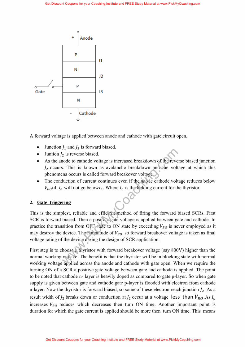
The time variation of voltage across the thyristor and current through it during turn on and turn off process gives the dynamic or switching characteristic of SCR.
Switching characteristic during turn on
Turn on time
It is the time during which it changes from forward blocking state to ON state. Total turn on time is divided into 3 intervals:
1. Delay time 2. Rise time 3. Spread time
Delay time
If 𝐼𝑔and 𝐼𝑎 represent the final value of gate current and anode current. Then the delay time can be explained as time during which the gate current attains 0.9 𝐼𝑔 to the instant anode current reaches 0.1 𝐼𝑔 or the anode current rises from forward leakage current to 0.1 𝐼𝑎.
1. Gate current 0.9 𝐼𝑔 to 0.1 𝐼𝑎. 2. Anode voltage falls from 𝑉𝑎 to 0.9𝑉𝑎. 3. Anode current rises from forward leakage current to 0.1 𝐼𝑎.
Get Discount Coupons for your Coaching Institute and FREE Study Material at www.PickMyCoaching.com
Get Discount Coupons for your Coaching Institute and FREE Study Material at www.PickMyCoaching.com
www.Pick
MyCoa
ching
.com

Rise time (𝒕𝒓)
Time during which
1. Anode current rises from 0.1 𝐼𝑎 to 0.9 𝐼𝑎 2. Forward blocking voltage falls from 0.9𝑉𝑎 to 0.1𝑉𝑎. 𝑉𝑎 is the initial forward blocking
voltage.
Spread time (𝒕𝒑)
1. Time taken by the anode current to rise from 0.9𝐼𝑎 to𝐼𝑎. 2. Time for the forward voltage to fall from 0.1𝑉𝑜 to on state voltage drop of 1 to 1.5V.
During turn on, SCR is considered to be a charge controlled device. A certain amount of charge is injected in the gate region to begin conduction. So higher the magnitude of gate current it requires less time to inject the charges. Thus turn on time is reduced by using large magnitude of gate current.
How the distribution of charge occurs?
As the gate current begins to flow from gate to cathode with the application of gate signal. Gate current has a non uniform distribution of current density over the cathode surface. Distribution of current density is much higher near the gate. The density decrease as the distance from the gate increases. So anode current flows in a narrow region near gate where gate current densities are highest. From the beginning of rise time the anode current starts spreading itself. The anode current spread at a rate of 0.1mm/sec. The spreading anode current requires some time if the rise time is not sufficient then the anode current cannot spread over the entire region of cathode. Now a large anode current is applied and also a large anode current flowing through the SCR. As a result turn on losses is high. As these losses occur over a small conducting region so local hot spots may form and it may damage the device.
Switching Characteristics During Turn Off
Thyristor turn off means it changed from ON to OFF state. Once thyristor is oON there is no role of gate. As we know thyristor can be made turn OFF by reducing the anode current below the latching current. Here we assume the latching current to be zero ampere. If a forward voltage is applied across the SCR at the moment it reaches zero then SCR will not be able to block this forward voltage. Because the charges trapped in the 4-layer are still favourable for conduction and it may turn on the device. So to avoid such a case, SCR is reverse biased for some time even if the anode current has reached to zero.
So now the turn off time can be different as the instant anode current becomes zero to the instant when SCR regains its forward blocking capability.
𝑡𝑞=𝑡𝑟𝑟+𝑡𝑞𝑟
Where,
Get Discount Coupons for your Coaching Institute and FREE Study Material at www.PickMyCoaching.com
Get Discount Coupons for your Coaching Institute and FREE Study Material at www.PickMyCoaching.com
www.Pick
MyCoa
ching
.com
𝑡𝑞 is the turn off time,𝑡𝑟𝑟 is the reverse recovery time, 𝑡𝑞𝑟 is the gate recovery time
At 𝑡1 anode current is zero. Now anode current builds up in reverse direction with same 𝑑𝑣
𝑑𝑡 slope. This is due to the presence of charge carriers in the four layers. The reverse
recovery current removes the excess carriers from 𝐽1 and 𝐽3 between the instants 𝑡1 and𝑡3. At instant 𝑡3 the end junction 𝐽1 and 𝐽3 is recovered. But 𝐽2 still has trapped charges which decay due to recombination only so the reverse voltage has to be maintained for some more time. The time taken for the recombination of charges between 𝑡3 and 𝑡4 is called gate recovery time 𝑡𝑞𝑟. Junction 𝐽2 recovered and now a forward voltage can be applied across SCR.
The turn off time is affected by:
1. Junction temperature 2. Magnitude of forward current 𝑑𝑖
𝑑𝑡 during commutation.
Turn off time decreases with the increase of magnitude of reverse applied voltage.
GTO(Gate turn off thyristor)
Get Discount Coupons for your Coaching Institute and FREE Study Material at www.PickMyCoaching.com
Get Discount Coupons for your Coaching Institute and FREE Study Material at www.PickMyCoaching.com
www.Pick
MyCoa
ching
.com

A gate turn off thyristor is a pnpn device. In which it can be turned ON like an ordinary SCR by a positive gate current. However it can be easily turned off by a negative gate pulse of appropriate magnitude.
Conventional SCR are turned on by a positive gate signal but once the SCR is turned on gate loses control over it. So to turn it off we require external commutation circuit. These commutation circuits are bulky and costly. So due to these drawbacks GTO comes into existence.
The salient features of GTO are:
1. GTO turned on like conventional SCR and is turned off by a negative gate signal of sufficient magnitude.
2. It is a non latching device. 3. GTO reduces acoustic and electromagnetic noise.
It has high switching frequency and efficiency.
A gate turn off thyristor can turn on like an ordinary thyristor but it is turn off by negative gate pulse of appropriate magnitude.
Disadvantage
The negative gate current required to turn off a GTO is quite large that is 20% to 30 % of anode current
Advantage
It is compact and cost less
Switching performance
Get Discount Coupons for your Coaching Institute and FREE Study Material at www.PickMyCoaching.com
Get Discount Coupons for your Coaching Institute and FREE Study Material at www.PickMyCoaching.com
www.Pick
MyCoa
ching
.com

1. For turning ON a GTO first TR1is turned on. 2. This in turn switches on TR2 so that a positive gate current pulse is applied to turn on the
GTO. 3. Thyristor 𝑇1 is used to apply a high peak negative gate current pulse.
Gate turn-on characteristics
1. The gate turn on characteristics is similar to a thyristor. Total turn on time consists of delay time, rise time, spread time.
2. The turn on time can be reduced by increasing its forward gate current.
Get Discount Coupons for your Coaching Institute and FREE Study Material at www.PickMyCoaching.com
Get Discount Coupons for your Coaching Institute and FREE Study Material at www.PickMyCoaching.com
www.Pick
MyCoa
ching
.com
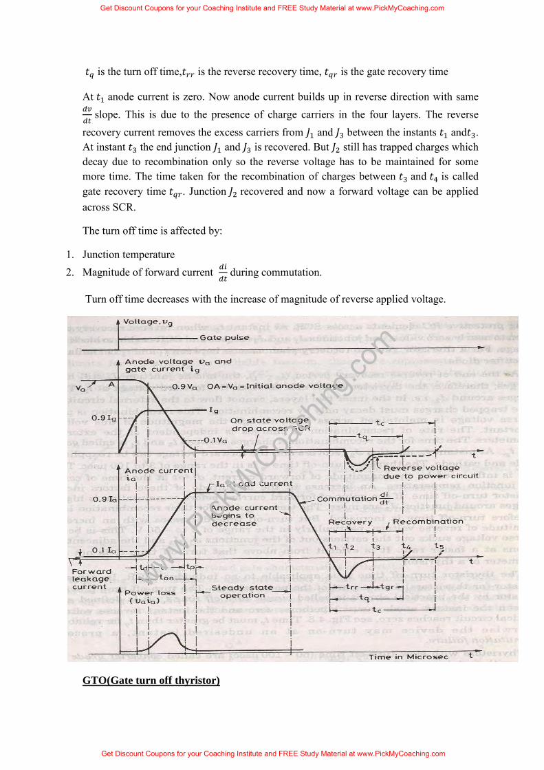
GATE TURN OFF
Turn off time is different for SCR.Turn off characteristics is divied into 3 pd
1. Storage time
2. Fall time
3. Tail time
Tq=ts+tf+tt
At normal operating condition gto carries a steady state current.The turn off process
starts as soon as negative current is applied after t=0.
STORAGE TIME
During the storagepd the anode voltage and current remains constant.The gate current rises
depending upon the gate circuit impedance and gate applied voltage.The beginning of pd is as soon
as negative gate current is applied.The end of storage pd is marked by fall in anode current and
rise in voltage,what we have to do is remove the excess carriers.the excess carriers are removed by
negative carriers.
Get Discount Coupons for your Coaching Institute and FREE Study Material at www.PickMyCoaching.com
Get Discount Coupons for your Coaching Institute and FREE Study Material at www.PickMyCoaching.com
www.Pick
MyCoa
ching
.com

FALL TIME
After ts, anode current begins to fall rapidly and anode voltage starts rising.After falling to a certain
value,then anode current changes its rate to fall.this time is called fall time.
SPIKE IN VOLTAGE
During the time of storage and fall timethere is achange in voltage due to abrupt current change.
TAIL TIME
During this time ,the anode current and voltage continues towards the turn off values.The transient
overshoot is due to the snubber parameter and voltage stabilizes to steady state value.
Get Discount Coupons for your Coaching Institute and FREE Study Material at www.PickMyCoaching.com
Get Discount Coupons for your Coaching Institute and FREE Study Material at www.PickMyCoaching.com
www.Pick
MyCoa
ching
.com
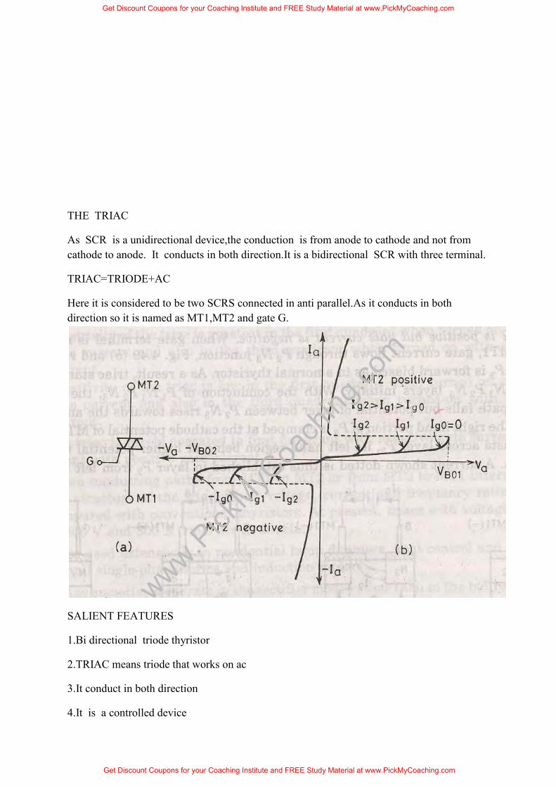
THE TRIAC
As SCR is a unidirectional device,the conduction is from anode to cathode and not from cathode to anode. It conducts in both direction.It is a bidirectional SCR with three terminal.
TRIAC=TRIODE+AC
Here it is considered to be two SCRS connected in anti parallel.As it conducts in both direction so it is named as MT1,MT2 and gate G.
SALIENT FEATURES
1.Bi directional triode thyristor
2.TRIAC means triode that works on ac
3.It conduct in both direction
4.It is a controlled device
Get Discount Coupons for your Coaching Institute and FREE Study Material at www.PickMyCoaching.com
Get Discount Coupons for your Coaching Institute and FREE Study Material at www.PickMyCoaching.com
www.Pick
MyCoa
ching
.com

5.Its operation is similar to two devices connected in anti parallel with common gate connection.
6.It has 3 terminals MT1,MT2 and gate G
Its use is control of power in ac.
POWER BJT
Power BJT means a large voltage blocking in the OFF state and high current carrying capability in the
ON state. In most power application, base is the input terminal. Emitter is the common terminal.
Collector is the output terminal.
SIGNAL LEVEL OF BJT
n+ doped emitter layer ,doping of base is more than collector.Depletion layer exists more towards
the collector than emitter
Get Discount Coupons for your Coaching Institute and FREE Study Material at www.PickMyCoaching.com
Get Discount Coupons for your Coaching Institute and FREE Study Material at www.PickMyCoaching.com
www.Pick
MyCoa
ching
.com

POWER BJT CONSTRUCTION
The maxium collector emitter voltage that can be sustained across the junction, when it is carrying substantial collector current.
Vceo=maxium collectorand emitter voltage that can be sustain by the device.
Vcbo=collector base breakdown voltage with emitter open
PRIMARY BREAKDOWN
It is due to convention avalanche breakdown of the C-B junction and its associated large flow of current.The thickness of the depletion region determines the breakdown voltage of the transistor.The base thickness is made as small as possible,in order to have good amplification capability. If the thickness is too small, the breakdown voltage is compromised.So a compromise has to be made between the two.
Get Discount Coupons for your Coaching Institute and FREE Study Material at www.PickMyCoaching.com
Get Discount Coupons for your Coaching Institute and FREE Study Material at www.PickMyCoaching.com
www.Pick
MyCoa
ching
.com

THE DOPING LEVELS-
1.The doping of the emitter layer is quite large.
2.The base doping is moderate.
3.n- region is lightly doped.
4.n+ region doping level is similar to emitter.
1.THICKNESS OF DRIFT REGION-
It determines the breakdown length of the transistor.
2.THE BASE THICKNES –
Small base thickness- good amplification capability
Too small base thickness- the breakdown voltage of the transistor has ti be compromised.
For a relatively thick base,the current gain will be relatively small.so it is increase the gain.Monolithicesigns for darlington connected BJT pair have been deveploed.
SECONDARY BREAKDOWN
Secondary breakdown is due to large power disspation at localized site within the semi conductor.
PHYSICS OF BJT OPERATION-
The transistor is assumed to operate in active region. There is no doped collector drift region. It has importance only in switching operation, in active region of operation.
B-E junction is forward biased and C-B junction is reverse biased. Electrons are injected into base from the emitter. Holes are injected from base into the emitter.
QUASI SATURATION-
Intially we assume that, the transistor is in active region. Base current is allowed to increase then lets see what happens.first collector rises in response to base current.So there is a increase voltage drop across the collector load.So C-E voltage drops.
Because of increase in collector current, there is a increase in voltage in drift region. This eventually reduces the reverse biased across the C-B junction.so n-p junction get smaller, at some point the junction become forward bised. So now injection of holes from base into collector drift region occurs. Charge neutrality requires the electron to be injected in the drift region of the holes. From where these electron came. Since a large no of electron is supplied to the C-B junction via injection from emitter and subsequent diffusion across the base. As excess carrier build up in the drift region begins to occur quasi saturation region is entered. As the injected carrires increase in the drift region is
Get Discount Coupons for your Coaching Institute and FREE Study Material at www.PickMyCoaching.com
Get Discount Coupons for your Coaching Institute and FREE Study Material at www.PickMyCoaching.com
www.Pick
MyCoa
ching
.com

gradually shotred out and the voltage across the drift region drops. In quasi saturation the drift region is not completely shorted out by high level injection.Hard saturation obtained when excess carrier density reaches the n+ side.
During quasi saturation, the rate of the collector fall.Hard saturation occurs when excess carriers have completely swept across the drift region .
THYRISTOR PROTECTION
OVER VOLTAGE PROTECTION
Over voltage occurring during the switching operation causes the failure of SCR.
INTERNAL OVERVOLTAGE
It is due to the operating condition of SCR.
Get Discount Coupons for your Coaching Institute and FREE Study Material at www.PickMyCoaching.com
Get Discount Coupons for your Coaching Institute and FREE Study Material at www.PickMyCoaching.com
www.Pick
MyCoa
ching
.com

During the commutation of SCR ,when the anode current decays to zero anode current reverses due to stored changes. First the reverse current rises to peak value, then reverse current reduces abruptly with large 𝑑𝑖
𝑑𝑡⁄ . During series inductance of SCR large
transient large voltage i.e 𝐿 𝑑𝑖𝑑𝑡⁄ . is generated.
EXTERNAL OVER VOLTAGE
This is due to external supply and load condition. This is because of
1. The interruption of current flow in an inductive circuit. 2. Lightening strokes on the lines feeding the thyristor systems.
Suppose a SCR converter is fed from a transformer, voltage transient occur when transformer primary will energise or de-energised.
This overvoltages cause random turn ON of a SCR. The effect of overvoltage is minimized using 1. RC circuits 2. Non linear resistor called voltage clamping device.
Voltage clamping device is a non linear resistor.It is connected between cathode and anode of SCR. The resistance of voltage clamping device decreases with increasing voltages. During normal working condition Voltage clamping (V.C) device has high resistance, drawing only leakage current. When voltage surge appears voltage clamping device offers a low resistance and it create a virtual short circuit across the SCR. Hence voltage across SCR is clamped to a safe value.
Get Discount Coupons for your Coaching Institute and FREE Study Material at www.PickMyCoaching.com
Get Discount Coupons for your Coaching Institute and FREE Study Material at www.PickMyCoaching.com
www.Pick
MyCoa
ching
.com

When surge condition over voltage clamping device returns to high resistance state. e.g. of voltage clamping device 1.Seleniumthyrector diodes 2.Metal Oxide varistors 3.Avalanche diode supressors OVER CURRENT PROTECTION Long duration operation of SCR, during over current causes the 1.junction temp. of SCR to rise above the rated value,causing permanent damage to device. SCR is protected from overcurrent by using 1.Circuit breakers 2.Fast acting fuses Proper co-ordination is essential because 1..fault current has to be interrupted before SCR gets damaged. 2.only faulty branches of the network has to be replaced. In stiff supply network,source has negligible impedance.So in such system the magnitude and rate of rise of current is not limited.Fault current hence junction temp rises in a few miliseconds. POINTS TO BE NOTED- 1. Proper coordination between fast acting fuse and thyristor is essential. 2. The fuse is always rated to carry marginal overload current over
definite period. 3. The peak let through current through SCR must be less than sub cycle
rating of the SCR. 4. The voltage across the fuse during arcing time is called arcing or
recovery voltage and is equal to sum of the source voltage and emf induced in the circuit inductance during arcing time.
5. On abrupt interruption of fuse current, induce emf would be high, which results in high arcing voltage.
Circuit Breaker (C.B)
C.B. has long tripping time. So it is used for protecting the device against continuous overload current or against the surge current for long duration. In order that fuse protects the thyristor realiably the 𝐼2𝑡 rating of fuse current must be less than that of SCR.
ELECTRONIC CROWBAR PROTECTION
Get Discount Coupons for your Coaching Institute and FREE Study Material at www.PickMyCoaching.com
Get Discount Coupons for your Coaching Institute and FREE Study Material at www.PickMyCoaching.com
www.Pick
MyCoa
ching
.com

For overcurrent protection of power converter using SCR, electronic crowbar are used. It provide rapid isolation of power converter before any damage occurs.
HEAT PROTECTION-
To protect the SCR
1. From the local spots
2. Temp rise
SCRs are mounted over heat sinks.
GATE PROTECTION-
Gate circuit should also be protected from
1. Overvoltages
2. Overcurrents
Overvoltage across the gate circuit causes the false triggering of SCR
Get Discount Coupons for your Coaching Institute and FREE Study Material at www.PickMyCoaching.com
Get Discount Coupons for your Coaching Institute and FREE Study Material at www.PickMyCoaching.com
www.Pick
MyCoa
ching
.com

Overcurrent raise the junction temperature. Overvoltage protection is by zener diode across
the gate circuit.
INSULATED GATE BIPOLAR TRANSISTOR(IGBT)-
BASIC CONSTRUCTION-
The n+ layer substrate at the drain in the power MOSFET is substituted by p+ layer substrate
and called as collector. When gate to emitter voltage is positive,n- channel is formed in the
p- region.This n- channel short circuit the n- and n+ layer and an electron movement in n
channel cause hole injection from p+subtrate layer to n- layer.
Get Discount Coupons for your Coaching Institute and FREE Study Material at www.PickMyCoaching.com
Get Discount Coupons for your Coaching Institute and FREE Study Material at www.PickMyCoaching.com
www.Pick
MyCoa
ching
.com

POWER MOSFET
A power MOSFET has three terminal device. Arrow indicates the direction of current flow. MOSFET is a voltage controlled device. The operation of MOSFET depends on flow of majority carriers only.
(Circuit diagram) (circuit symbol)
Switching Characteristics:-
The switching characteristic is influenced by
1. Internal capacitance of the device.
2. Internal impedance of the gate drive circuit.
Total turn on time is divided into
1.Turn on delay time
2.Rise time
Turn on time is affected by impedance of gate drive source. During turn on delay time gate to source voltage attends its threshold value 𝑉𝐺𝑆𝑇.
After 𝑡𝑑𝑛 and during rise time gate to source voltage rise to 𝑉𝐺𝑠𝑝, a voltage which is sufficient to drive the MOSFET to ON state.
The turn off process is initiated by removing the gate to source voltage. Turn off time is composed of turn off delay time to fall time.
Turn off delay time
Get Discount Coupons for your Coaching Institute and FREE Study Material at www.PickMyCoaching.com
Get Discount Coupons for your Coaching Institute and FREE Study Material at www.PickMyCoaching.com
www.Pick
MyCoa
ching
.com

To turn off the MOSFET the input capacitance has to be discharged . During 𝑡𝑑𝑓 the input capacitance discharge from 𝑉1to 𝑉𝐺𝑠𝑝. During 𝑡𝑓 , fall time ,the input capacitance discharges from 𝑉𝐺𝑠𝑝 to 𝑉𝐺𝑆𝑇. During 𝑡𝑓 drain current falls from 𝐼𝐷 to zero.
So when 𝑉𝐺𝑠 ≤ 𝑉𝐺𝑆𝑇 , MOFSET turn off is complete.
Fig. Switching waveform of power MOSFET
Insulated Gate Bipolar Transistor (IGBT)
IGBT has high input impedance like MOFFSET and low on state power lose as in BJT.
IGBT Characteristics
Here the controlling parameter is gate emitter voltage As IGBT is a voltage controlled device.
When 𝑉𝐺𝐸 is less than 𝑉𝐺𝐸𝑇 that is gate emitter threshold voltage IGBT is in off state.
Get Discount Coupons for your Coaching Institute and FREE Study Material at www.PickMyCoaching.com
Get Discount Coupons for your Coaching Institute and FREE Study Material at www.PickMyCoaching.com
www.Pick
MyCoa
ching
.com

Fig. a Fig. b. Fig. c
Fig. a (Circuit diagram for obtaining V-I characteristics) Fig. b (Static V-I characteristics)
Fig. c (Transfer characteristic)
Switching characteristics: Figure below shows the turn ON and turn OFF characteristics of IGBT
Turn on time
Get Discount Coupons for your Coaching Institute and FREE Study Material at www.PickMyCoaching.com
Get Discount Coupons for your Coaching Institute and FREE Study Material at www.PickMyCoaching.com
www.Pick
MyCoa
ching
.com
Time between the instants forward blocking state to forward on -state .
Turn on time = Delay time + Rise time
Delay time = Time for collector emitter voltage fall from 𝑉𝐶𝐸 to 0.9𝑉𝐶𝐸
𝑉𝐶𝐸=Initial collector emitter voltage
𝑡𝑑𝑛=collector current to rise from initial leakage current to 0.1Ic
Ic= Final value of collector current
Rise time
Collector emitter voltage to fall from 0.9𝑉𝐶𝐸 to 0.1𝑉𝐶𝐸 .
0.1Ic to Ic
After 𝑡𝑜𝑛 the device is on state the device carries a steady current of Ic and the collector emitter voltage falls to a small value called conduction drop 𝑉𝐶𝐸𝑆.
Turn off time
1) Delay time 𝑡𝑑𝑓
2) Initial fall time 𝑡𝑓1
3) Final fall time 𝑡𝑓2
𝑡𝑂𝑓𝑓 =𝑡𝑑𝑓
+ 𝑡𝑓1+ 𝑡𝑓2
𝑡𝑑𝑓= Time during which the gate emitter voltage falls to the threshold value 𝑉𝐺𝐸𝑇.
Collector current falls from Ic to 0.9Ic at the end of the 𝑡𝑑𝑓 collector emitter voltage begins to
rise.
Turn off time = Collector current falls from 90% to 20% of its initial value Ic OR The time during which collector emitter voltage rise from 𝑉𝐶𝐸 to 0.1𝑉𝐶𝐸.
𝑡𝑓2= collector current falls from20% to 10% of Ic.
During this collector emitter voltage rise 0.1𝑉𝐶𝐸 to final value of 𝑉𝐶𝐸.
Series and parallel operation of SCR
SCR are connected in series for h.v demand and in parallel for fulfilling high current demand. Sting efficiency can be defined as measure of the degree of utilization on SCRs in a string.
String efficiency < 1.
Derating factor (DRF)
Get Discount Coupons for your Coaching Institute and FREE Study Material at www.PickMyCoaching.com
Get Discount Coupons for your Coaching Institute and FREE Study Material at www.PickMyCoaching.com
www.Pick
MyCoa
ching
.com

1 – string efficiency.
If DRF more then
no. of SCRs will more, so string is more reliable.
Let the rated blocking voltage of the string of a series connected SCR is 2𝑉1 as shown in the figure below, But in the string two SCRs are supplied a maximum voltage of 𝑉1+𝑉2.
𝜂 =𝑉1 + 𝑉2
2𝑉1
Significance of string efficiency .
Two SCRs are have same forward blocking voltage ,When system voltage is more then the voltage rating of a single SCR. SCRs are connected in series in a string.
There is a inherent variation in characteristics. So voltage shared by each SCR may not be equal. Suppose, SCR1 leakage resistance > SCR2 leakage resistance. For same leakage current 𝐼0 in the series connected SCRs. For same leakage current SCR1 supports a voltage 𝑉1 , SCR2 supports a voltage 𝑉2,
So string 𝜂 for two SCRs = 𝑉1+𝑉2
2𝑉2 = 1
2(1 +
𝑉2
𝑉1) < 1 .
So, 𝑉1 > 𝑉2,
The above operation is when SCRs are not turned ON. But in steady state of operation , A uniform voltage distribution in the state can be achieved by connect a suitable resistance across each SCRs , so that parallel combination have same resistance.
But this is a cumbersome work. During steady state operation we connect same value of shunt resistance across each SCRs. This shunt resistance is called state equalizing circuit.
Suppose,
Get Discount Coupons for your Coaching Institute and FREE Study Material at www.PickMyCoaching.com
Get Discount Coupons for your Coaching Institute and FREE Study Material at www.PickMyCoaching.com
www.Pick
MyCoa
ching
.com
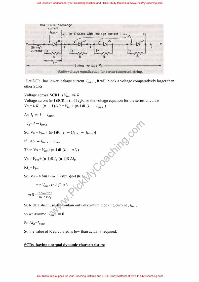
Let SCR1 has lower leakage current 𝐼𝑏𝑚𝑛 , It will block a voltage comparatively larger than other SCRs.
Voltage across SCR1 is 𝑉𝑏𝑚 =𝐼1𝑅. Voltage across (n-1)SCR is (n-1) 𝐼2R, so the voltage equation for the series circuit is Vs = 𝐼1𝑅+ (𝑛 − 1)𝐼2𝑅 = 𝑉𝑏𝑚+ (n-1)R (𝐼 − 𝐼𝑏𝑚𝑥 )
As 𝐼1 = 𝐼 − 𝐼𝑏𝑚𝑛
𝐼2= 𝐼 − 𝐼𝑏𝑚𝑥
So, Vs = 𝑉𝑏𝑚+ (n-1)R [𝐼1 − (𝐼𝑏𝑚𝑥 − 𝐼𝑏𝑚𝑛)]
If Δ𝐼𝑏 = 𝐼𝑏𝑚𝑥 − 𝐼𝑏𝑚𝑛
Then Vs = 𝑉𝑏𝑚+(n-1)R (𝐼1 − Δ𝐼𝑏)
Vs = 𝑉𝑏𝑚+ (n-1)R 𝐼1-(n-1)R Δ𝐼𝑏
R𝐼1= 𝑉𝑏𝑚
So, Vs = 𝑉𝑏𝑚+ (n-1) 𝑉𝑏𝑚 -(n-1)R Δ𝐼𝑏
= n 𝑉𝑏𝑚- (n-1)R Δ𝐼𝑏
⇒R = 𝑛𝑉𝑏𝑚−𝑉𝑆
(n−1)Δ𝐼𝑏
SCR data sheet usually contain only maximum blocking current , 𝐼𝑏𝑚𝑥
so we assume 𝐼𝑏𝑚𝑛 = 0
So Δ𝐼𝑏=𝐼𝑏𝑚𝑥
So the value of R calculated is low than actually required.
SCRs having unequal dynamic characteristics:
Get Discount Coupons for your Coaching Institute and FREE Study Material at www.PickMyCoaching.com
Get Discount Coupons for your Coaching Institute and FREE Study Material at www.PickMyCoaching.com
www.Pick
MyCoa
ching
.com

It may occur that SCRS may have unequal dynamic characteristics so the voltage distribution across the SCR may be unequal during the transient condition.
SCR 1 and SCR 2 have different dynamic characteristics. Turn ON time of SCR 2 is more than SCR 1 by time Δ𝑡𝑑 .
As string voltage is 𝑉𝑆 so voltage shared by each SCRs be 𝑉𝑆/2. Now both are gated at same time so SCR 1 will turn ON at 𝑡1 its voltage fall nearly to zero so the voltage shared by SCR 2 will be the string voltage if the break over voltage of SCR 2 is less than 𝑉𝑆 then SCR 2 will turn ON .
* In case 𝑉𝑆 is less than the breakoverer voltage, SCR 2 will turn ON at instant 2. SCR 1 assumed to have less turn off 𝑡𝑞1
time then SCR 2, so 𝑡𝑞1< 𝑡𝑞2
. At 𝑡2 SCR 1 has recovered while SCR 2 is developing recovery voltage at 𝑡1 both are developing different reverse recovery voltage. At 𝑡2 SCR 1 has recovered while SCR2 is developing reverse recovery voltage .
Conclusion :
* Series connected SCR develop different voltages during turn ON and turn OFF process. Till now we connect a simple resistor across the diode for static voltage equalizing circuit .
* During turn ON and turn OFF capacitance of reverse biased junction determine the voltage distribution across SCRs in a series connected string . As reverse biased junction have different capacitance called self capacitance , the voltage distribution during turn ON and turn Off process would be different.
Get Discount Coupons for your Coaching Institute and FREE Study Material at www.PickMyCoaching.com
Get Discount Coupons for your Coaching Institute and FREE Study Material at www.PickMyCoaching.com
www.Pick
MyCoa
ching
.com

* Under transient condition equal voltage distribution can be achieved by employing shunt capacitance as this shunt capacitance has the effect of that the resultant of shunt and self capacitance tend to be equal. The capacitor is used to limits the dv/dt across the SCR during forward blocking state. When this SCR turned ON capacitor discharges heavy current through the SCR . The discharge current spike is limited by damping resistor 𝑅𝑐 . 𝑅𝑐 also damps out high frequency oscilation that may arise due to series combination of 𝑅𝑐 ,C and series inductor . 𝑅𝑐 & C are called dynamic equalizing circuit
Diode D is used during forward biased condition for more effective charging of the capacitor. During capacitor discharge 𝑅𝑐 comes into action for limiting current spike and rate of change of current di/dt .
The R, 𝑅𝑐 & C component also provide path to flow reverse recovery current. When one SCR regain its voltage blocking capability. The flow of reverse recovery current is necessary as it facilitates the turning OFF process of series connected SCR string. So C is necessary for both during turn ON and turn OFF process. But the voltage unbalance during turn OFF time is more predominant then turn ON time. So choice of C is based on reverse recovery characteristic of SCR .
Get Discount Coupons for your Coaching Institute and FREE Study Material at www.PickMyCoaching.com
Get Discount Coupons for your Coaching Institute and FREE Study Material at www.PickMyCoaching.com
www.Pick
MyCoa
ching
.com

SCR 1 has short recovery time as compared to SCR 2. Δ𝑄 is the difference in reverse recovery charges of two SCR 1 and SCR 2. Now we assume the SCR 1 recovers fast . i.e it goes into blocking state so charge Δ𝑄 can pass through C . The voltage induced by 𝑐1 is 𝛥𝑄/C , where is no voltage induced across 𝐶2 .
The difference in voltage to which the two shunt capacitor are charged is 𝛥𝑄/C .
Now thyristor with least recovery time will share the highest transient voltage say 𝑉𝑏𝑚,
So, 𝑉𝑏𝑚 - 𝑉2 = Δ𝑄/C
So, 𝑉2= 𝑉𝑏𝑚 - Δ𝑄/C
As 𝑉1 = 𝑉𝑏𝑚
𝑉𝑆 = 𝑉1+𝑉2
= 𝑉𝑏𝑚+(𝑉𝑏𝑚 - Δ𝑄/C)
𝑉𝑆 = 2𝑉𝑏𝑚-Δ𝑄/C
⇒ 12
(𝑉𝑠 +Δ𝑄
𝐶) = 𝑉𝑏𝑚
⇒ 𝑉2= 𝑉𝑏𝑚 - Δ𝑄/C
12[𝑉𝑠 - Δ𝑄/C]
Now suppose that there are n series SCRs in a string.
Get Discount Coupons for your Coaching Institute and FREE Study Material at www.PickMyCoaching.com
Get Discount Coupons for your Coaching Institute and FREE Study Material at www.PickMyCoaching.com
www.Pick
MyCoa
ching
.com

Let us assume that if top SCR has similar to characteristic SCR 1. Then SCR 1 would support a voltage 𝑉𝑏𝑚
* If the remaining (n-1) SCR has characteristic that of SCR 2 .Then SCR 1 would recover first and support a voltage 𝑉𝑏𝑚 . The charge (n-1) Δ𝑄 from the remaining (n -1) SCR would pass through C.
𝑉1 = 𝑉𝑏𝑚
𝑉2 = 𝑉𝑏𝑚 - Δ𝑄/C
Voltage across (n-1) slow thyristors
𝑉 = (n-1) (𝑉𝑏𝑚 - Δ𝑄/C)
So, 𝑉𝑆 = V1+(n-1) 𝑉2
= 𝑉𝑏𝑚 + (n-1) (𝑉𝑏𝑚 - Δ𝑄/C)
By simplifing we get ,
𝑉𝑏𝑚 = 1𝑛 [𝑉𝑠+(n-1) Δ𝑄/C ]
C =[ (n-1) Δ𝑄/( n𝑉𝑏𝑚 -𝑉𝑆)
𝑉2 = (𝑉𝑆 - Δ𝑄/C )/ n .
Parallel operation:
When current required by the load is more than the rated current of single thyristor , SCRs are connected in parallel in a string .
Get Discount Coupons for your Coaching Institute and FREE Study Material at www.PickMyCoaching.com
Get Discount Coupons for your Coaching Institute and FREE Study Material at www.PickMyCoaching.com
www.Pick
MyCoa
ching
.com
For equal sharing of current, SCRs must have same 𝑉 − 𝐼characteristics during forward conduction. 𝑉𝑇 across them must be same. For same 𝑉𝑇 , SCR 1 share 𝐼1and SCR 2 share I2 .
If 𝐼1 is the rated current
𝐼2 < 𝐼1
The total current 𝐼1+𝐼2 and not rated current 2𝐼1.Type equation here.
Thus string efficiency ,
𝐼1+. 𝐼22𝐼1
= 12
(1 +𝐼𝐼2𝐼1
)
Middle conductor will have more inductance as compared to other two nearby conductor. As a result less current flow through the middle conductor. Another method is by magnetic coupling.
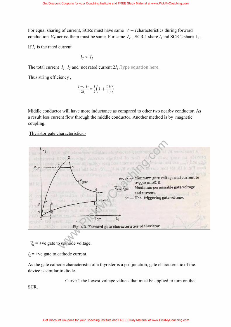
Thyristor gate characteristics:-
𝑉𝑔 = +ve gate to cathode voltage.
𝐼𝑔= +ve gate to cathode current.
As the gate cathode characteristic of a thyrister is a p-n junction, gate characteristic of the device is similar to diode.
Curve 1 the lowest voltage value s that must be applied to turn on the SCR.
Get Discount Coupons for your Coaching Institute and FREE Study Material at www.PickMyCoaching.com
Get Discount Coupons for your Coaching Institute and FREE Study Material at www.PickMyCoaching.com
www.Pick
MyCoa
ching
.com

Curve 2 highest possible voltage values that can be safely applied to get circuit.
𝑉gm= Maximum limit for gate voltage .
𝐼gm= Maximum imilt for gate current.
𝑃gav = Rated gate power dissipation for each SCR.
These limits should not be crossed in order to avoid the permanent damage of the device junction 𝐽3.
OY = Minimum limit of gate voltage to turn ON .
OX = minimum limit of gate current to turn ON.
If 𝑉gm, 𝐼gm, 𝑃gav are exceeded the thyristor will damage so the preferred gate drive area of SCR is bcdefghb.
oa = The non triggering gate voltage , If firing circuit generates +ve gate signal prior to the desired instant of triggering the SCR.It should be ensured that this un wanted signal should be less than the non –triggering voltage oa.
𝐸𝑆 = 𝑉𝑔 + 𝐼𝑔𝑅𝑆
𝐸𝑆 =Gate source voltage
𝑉𝑔 = Gate cathode voltage
𝐼𝑔 = Gate current
𝑅𝑆 = Gate source resistance
𝑅𝑆 = The internal resistance of the trigger source
𝑅1 is connected across the gate cathode terminal, which provides an easy path to the flow of leakage current between SCR terminal. If 𝐼𝑔𝑚𝑛 , 𝑉gmn are the minimum gate current and gate voltage to turn ON the SCR.
𝐸𝑆 = (𝐼𝑔𝑚𝑛+ 𝑉gmn/ 𝑅1) 𝑅𝑆 + 𝑉𝑔𝑚𝑛
Get Discount Coupons for your Coaching Institute and FREE Study Material at www.PickMyCoaching.com
Get Discount Coupons for your Coaching Institute and FREE Study Material at www.PickMyCoaching.com
www.Pick
MyCoa
ching
.com

MODULE-II
Get Discount Coupons for your Coaching Institute and FREE Study Material at www.PickMyCoaching.com
Get Discount Coupons for your Coaching Institute and FREE Study Material at www.PickMyCoaching.com
www.Pick
MyCoa
ching
.com

RECTIFIER
Rectifier are used to convert A.C to D.C supply.
Rectifiers can be classified as single phase rectifier and three phase rectifier. Single phase rectifier are classified as 1-Փ half wave and 1-Փ full wave rectifier. Three phase rectifier are classified as 3-Փ half wave rectifier and 3-Փ full wave rectifier. 1-Փ Full wave rectifier are classified as1-Փ mid point type and 1-Փ bridge type rectifier. 1-Փ bridge type rectifier are classified as 1-Փ half controlled and 1-Փ full controlled rectifier. 3-Փ full wave rectifier are again classified as 3-Փ mid point type and 3-Փ bridge type rectifier. 3-Փ bridge type rectifier are again divided as 3-Փ half controlled rectifier and 3-Փ full controlled rectifier.
Single phase half wave circuit with R-L load
Output current 𝑖𝑜 rises gradually. After some time 𝑖𝑜 reaches a maximum value and then begins to decrease.
At π, 𝑣𝑜=0 but 𝑖𝑜 is not zero because of the load inductance L. After π interval SCR is reverse biased but load current is not less then the holding current.
At β>π, 𝑖𝑜 reduces to zero and SCR is turned off.
At 2π+β SCR triggers again
α is the firing angle.
Get Discount Coupons for your Coaching Institute and FREE Study Material at www.PickMyCoaching.com
Get Discount Coupons for your Coaching Institute and FREE Study Material at www.PickMyCoaching.com
www.Pick
MyCoa
ching
.com

β is the extinction angle.
v conduction angle
Analysis for 𝑉𝑇 .
At 𝜔𝑡 = 𝐼,𝑉𝑇 = 𝑉𝑚𝑠𝑖𝑛𝐼
During = 𝐼 𝑡𝑜 𝐼 , 𝑉𝑇 = 0;
When = 𝐼 , 𝑉𝑇 = 𝑉𝑚𝑠𝑖𝑛𝐼;
00sinm
diV t Ri Ldt
2 2sin( t )m
sVi
R X
Where,
1tan XR
X L
Where 𝐼 is the angle by which 𝐼𝑠 lags 𝑉𝑠.
The transient component can be obtained as
0 0tdiRi Ldt
So 𝑖𝑡 = 𝐴𝑒−(𝑅𝑡 𝐿)⁄
𝑖0 = 𝑖𝑠 + 𝑖𝑡
𝑉𝑚
𝑧sin( 𝜔𝑡 − 𝐼) + 𝐴𝑒−(𝑅𝑡 𝐿)⁄
Where 𝑧 = √𝑅2 + 𝑋2
At 𝛼 = 𝜔𝑡, 𝑖𝑜 = 0;
0 =𝑉𝑚
𝑧sin( 𝛼 − 𝐼) + 𝐴𝑒−(𝑅𝛼 𝐿𝜔)⁄ ;
𝐴 =−𝑉𝑚
𝑧sin( 𝛼 − 𝐼)𝑒(𝑅𝛼 𝐿𝜔)⁄
𝑖𝑜 =𝑉𝑚
𝑧sin( 𝜔𝑡 − 𝐼) −
𝑉𝑚
𝑧sin( 𝛼 − 𝐼)𝑒−𝑅(𝜔𝑡−𝛼) 𝐿𝜔⁄
Get Discount Coupons for your Coaching Institute and FREE Study Material at www.PickMyCoaching.com
Get Discount Coupons for your Coaching Institute and FREE Study Material at www.PickMyCoaching.com
www.Pick
MyCoa
ching
.com

Therefore,
𝜔𝑡 = 𝛽, 𝑖0 = 0;
So sin(𝛽 − 𝛼) = sin (𝛼 − 𝐼)𝑒−(𝛽−𝛼)/(𝜔𝐿)
β can obtained from the above equation.
The average load voltage can be given by
01 sin ( )
2 mV V td t
𝑉𝑚
2𝜋(cos(𝛼) − cos (𝛽))
Average load current
0 (cos cos )2
mVIR
Single phase full converter
01 sin( ) ( )mV V t d t
2 cosmV
T₁,T₂ triggered at α and π radian latter T₃, T₄ are triggered.
Get Discount Coupons for your Coaching Institute and FREE Study Material at www.PickMyCoaching.com
Get Discount Coupons for your Coaching Institute and FREE Study Material at www.PickMyCoaching.com
www.Pick
MyCoa
ching
.com
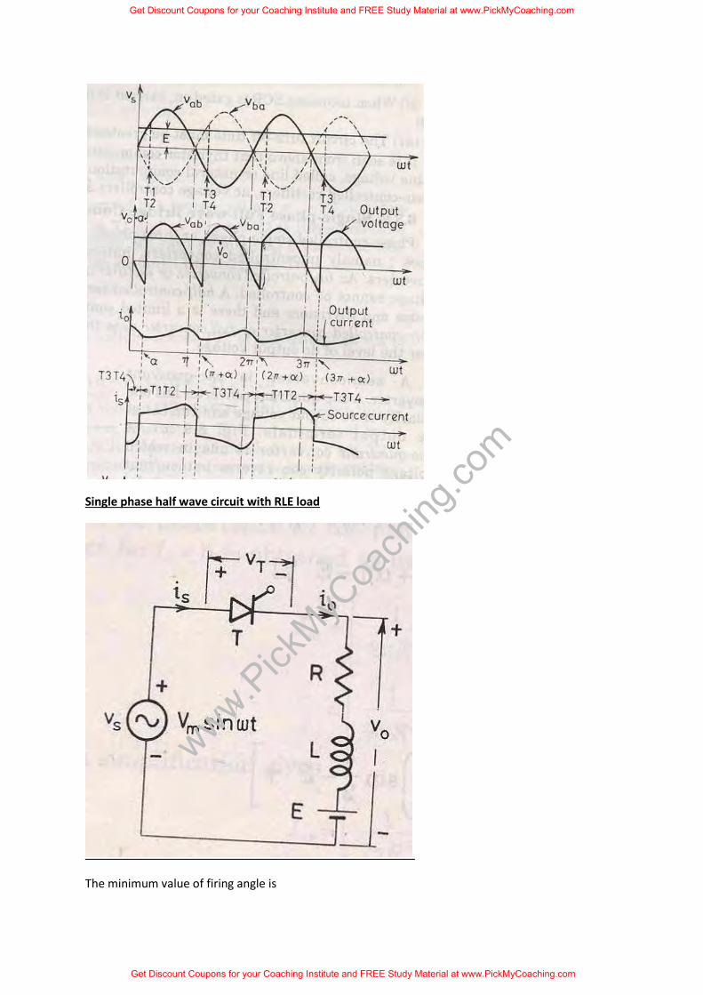
Single phase half wave circuit with RLE load
The minimum value of firing angle is
Get Discount Coupons for your Coaching Institute and FREE Study Material at www.PickMyCoaching.com
Get Discount Coupons for your Coaching Institute and FREE Study Material at www.PickMyCoaching.com
www.Pick
MyCoa
ching
.com

sin( )mV t E
So,
11 sin
m
EV
Maximum value of firing angle
2 2
The voltage differential equation is
00sin( )m
diV t Ri L Edt
1 2s s si i i
Due to source volt
1 sin( )ms
Vi tZ
Due to DC counter emf
Get Discount Coupons for your Coaching Institute and FREE Study Material at www.PickMyCoaching.com
Get Discount Coupons for your Coaching Institute and FREE Study Material at www.PickMyCoaching.com
www.Pick
MyCoa
ching
.com

2 ( / )si E R
( / )R L tti Ae
Thus the total current is given by
1 2s s ti i i
(R/L) tsin( )mV Et AeZ R
(R/L) t0 sin( )m
sV Ei t AeZ R
0 0At t i
[ sin( )]e R LmVEAR Z
So
{ ( )} { (
0 [sin( ) sin( ) [1 ]R Rt tm L LV Ei t e e
Z R
Average voltage across the inductance is zero. Average value of load current is
01I ( sin )d( )
2 mV t E tR
1 [ (cos cos )]2 mV
R
Conduction angle
v
01I [ (cos cos( ) )]
2 mV v vR
cos cosB 2sin sin2 2
A B A BA
So
01I [2 sin( )sin . ]
2 2 2mv vV E
R
Get Discount Coupons for your Coaching Institute and FREE Study Material at www.PickMyCoaching.com
Get Discount Coupons for your Coaching Institute and FREE Study Material at www.PickMyCoaching.com
www.Pick
MyCoa
ching
.com

0E I R
1E [2 sin( )sin . ]2 2 2m
v vV E
E(1 ) [ sin( )sin ]2 2 2
mVv v v
If load inductance L is zero then
2
And 2v
But 2 1
So 2 1
And 1v
So average current will be
0 1 11I [ (cos cos( )) ( )]
2 mV ER
So V0=E+I0R
11(cos cos ) (1 )
2 2mV E
For no inductance rms value of load current
2 1/20 2
1I [ ( sin( ) ) ]2 mV t E d t
R
Power delivered to load
20orP I R I E
Supply power factor
20or
s or
I R I EPfV I
Single phase full wave converter:
Get Discount Coupons for your Coaching Institute and FREE Study Material at www.PickMyCoaching.com
Get Discount Coupons for your Coaching Institute and FREE Study Material at www.PickMyCoaching.com
www.Pick
MyCoa
ching
.com

Get Discount Coupons for your Coaching Institute and FREE Study Material at www.PickMyCoaching.com
Get Discount Coupons for your Coaching Institute and FREE Study Material at www.PickMyCoaching.com
www.Pick
MyCoa
ching
.com

01 sin( ) ( )mV V t d t
2 sinmV
Single phase semi converter:
01 sin( ) ( )mV V t d t
cosmV
full converter:
Get Discount Coupons for your Coaching Institute and FREE Study Material at www.PickMyCoaching.com
Get Discount Coupons for your Coaching Institute and FREE Study Material at www.PickMyCoaching.com
www.Pick
MyCoa
ching
.com
steady state analysis
0s o
diV Ri L Edt
0 0V RI E
02 cosmVV
So in case of DC motor load
0 a a m mV r I
So
2 cosma a
mm
V r I
m aT I
ea
m
TI
Put
ea
m
TI
So 2
2( )cosm
a em
m m
Vr T
Get Discount Coupons for your Coaching Institute and FREE Study Material at www.PickMyCoaching.com
Get Discount Coupons for your Coaching Institute and FREE Study Material at www.PickMyCoaching.com
www.Pick
MyCoa
ching
.com

MODULE - III
Get Discount Coupons for your Coaching Institute and FREE Study Material at www.PickMyCoaching.com
Get Discount Coupons for your Coaching Institute and FREE Study Material at www.PickMyCoaching.com
www.Pick
MyCoa
ching
.com

CHOPPER
A chopper is a static device that converts fixed DC input voltage to variable output voltage
directly. Chopper are mostly used in electric vehicle, mini haulers.
Chopper are used for speed control and braking. The systems employing chopper offer
smooth control, high efficiency and have fast response.
The average output voltage is
1
0 1 10
1 1 (t )t
a s s sV V dt V ft V VT T
The average load current
a sa
V VIR R
Where, T=chopping period
Duty cycle of chopper =
1tT
f=chopping frequency
The rms value of output voltage is
12 2
0 00
1( ) sV V dt VT
If we consider the converter to be loss less then the input power is equal to the output power and is
given by
Get Discount Coupons for your Coaching Institute and FREE Study Material at www.PickMyCoaching.com
Get Discount Coupons for your Coaching Institute and FREE Study Material at www.PickMyCoaching.com
www.Pick
MyCoa
ching
.com

2
00 0
2 2
1 1
1 ( )
T To
i
s s
VP V idt dtT T R
V VTT R R
The effective input resistance seen by the P source is
s si
sa
V V RP VIR
The duty cycle α can be varied by varying t₁ , T of frequency.
Constant frequency operation:
1)The chopping period T is kept constant and on time is varied.
The pulse width modulation ,the width of the pulse is varied.
2) Variable frequency operation, the chopping frequency f is varied.
Frequency modulation, either on time or off time is kept constant.
This type of control generate harmonics at unpredictable frequency and filter design is often
difficult.
TYPES OF CHOPPER:
FIRST QUADRANT OR TYPE A CHOPPER:
When switch ON
0 sV V.
Get Discount Coupons for your Coaching Institute and FREE Study Material at www.PickMyCoaching.com
Get Discount Coupons for your Coaching Institute and FREE Study Material at www.PickMyCoaching.com
www.Pick
MyCoa
ching
.com
Current i₀ flows in the same direction when switch off.
V₀=0, i₀=0
So, average value of both the load and the current are positive.
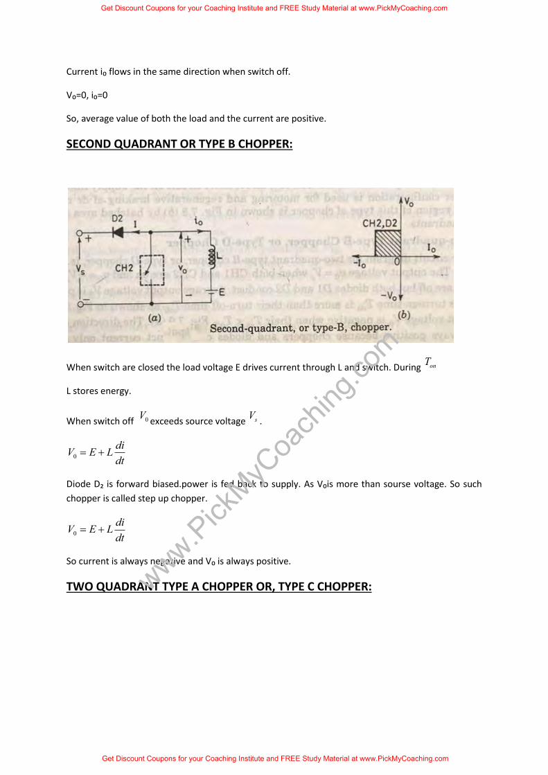
SECOND QUADRANT OR TYPE B CHOPPER:
When switch are closed the load voltage E drives current through L and switch. During onT
L stores energy.
When switch off 0Vexceeds source voltage sV
.
0diV E Ldt
Diode D₂ is forward biased.power is fed back to supply. As V₀is more than sourse voltage. So such
chopper is called step up chopper.
0diV E Ldt
So current is always negative and V₀ is always positive.
TWO QUADRANT TYPE A CHOPPER OR, TYPE C CHOPPER:
Get Discount Coupons for your Coaching Institute and FREE Study Material at www.PickMyCoaching.com
Get Discount Coupons for your Coaching Institute and FREE Study Material at www.PickMyCoaching.com
www.Pick
MyCoa
ching
.com

Both the switches never switch ON simultaneously as it lead direct short circuit of the
supply.
Now when sw2 is closed or FD is on the output voltage V₀ is zero.
When sw1 is ON or diode D conducts output voltage is V₀ is +Vs’
CURRENT ANANLYSIS:
When CH1 is ON current flows along i0. When CH1 is off current continues to flow along i0
as FD is forward biased. So i0 is positive.
Now when CH2 is ON current direction will be opposite to i0. When sw2 is off D2 turns ON.
Load current is –i0. So average load voltage is always positive. Average load current may be
positive or negative.
TWO QUADRANT TYPE B CHOPPER, OR TYPE D CHOPPER:
Get Discount Coupons for your Coaching Institute and FREE Study Material at www.PickMyCoaching.com
Get Discount Coupons for your Coaching Institute and FREE Study Material at www.PickMyCoaching.com
www.Pick
MyCoa
ching
.com

When CH1 and CH2 both are on then V0=Vs.
When CH1 and CH2 are off and D1 and D2 are on V 0=-Vs.
The direction of current is always positive because chopper and diode can only conduct in
the direction of arrow shown in fig.
Average voltage is positive when Ton>Toff
FOUR QUADRANT CHOPPER, OR TYPE E CHOPPER
Get Discount Coupons for your Coaching Institute and FREE Study Material at www.PickMyCoaching.com
Get Discount Coupons for your Coaching Institute and FREE Study Material at www.PickMyCoaching.com
www.Pick
MyCoa
ching
.com

FIRST QUADRANT:
CH4 is kept ON
CH3 is off
CH1 is operarted
V0=Vs
i0 = positive
when CH1 is off positive current free wheels through CH4,D2
so V0 and I2 is in first quadrant.
SECOND QUADRANT:
CH1,CH3,CH4 are off.
CH2 is operated.
Reverse current flows and I is negative through L CH2 D4 and E.
When CH2 off D1 and D4 is ON and current id fed back to source. So
diE Ldt
is more than source voltage Vs.
As i0 is negative and V0 is positive, so second quadrant operation.
THIRD QUADRANT:
CH1 OFF, CH2 ON
CH3 operated. So both V0 and i0 is negative.
When CH3 turned off negative current freewheels through CH2 and D4.
FOURTH QUADRANT:
Get Discount Coupons for your Coaching Institute and FREE Study Material at www.PickMyCoaching.com
Get Discount Coupons for your Coaching Institute and FREE Study Material at www.PickMyCoaching.com
www.Pick
MyCoa
ching
.com

CH4 is operated other are off.
Positive current flows through CH4 E L D2.
Inductance L stores energy when current fed to source through D3 and D2.V0 is negative.
STEADY STATE ANALYSIS OF PRACTICAL BUCK CHOPPER:
The voltage across the inductor L is ei=Ldi/dt.
2 1
1 1
( )s a
d i i iV V L Lt t
1s a
iLtV V
.
The inductor current falls linearly from I2 to I1 in time t2 as Vs =0.
So
1 2
2
L( )a
i iVt
If I2-I1=ΔI then
2a
L IVt
2a
L ItV
.
ΔI=I2-I1= peak to peak ripple current.
1 2( ) ts a aV V V tIL L
Now t1=αT, t2=(1-α)T
1a s s
tV V VT
Α<1 so it is a step down or buck converter.
If the circuit is lossless then VsIs=Va Ia=αVsIa
Is =α Ia.
Now switching period T can be expressed as
Get Discount Coupons for your Coaching Institute and FREE Study Material at www.PickMyCoaching.com
Get Discount Coupons for your Coaching Institute and FREE Study Material at www.PickMyCoaching.com
www.Pick
MyCoa
ching
.com

T=1/f= t1+ t2=ΔIL/(Vs-Va) + ΔIL/(Va)
=ΔILVs/Va(Vs-Va)
So peak to peak ripple current
( )a s a
s
V V VIfLV
(1 )aVIfL
The peak to peak voltage of the capacitor is
8cIVfc
So from above equation
2 2
( ) (1 ).8 8a s a s
cs
V V V VVLcf V Lcf
Condition for continuous inductor current and capacitor voltage :
If IL is the average inductor current
2L LI I ….as
a sV V
(1 )sVfL
As
2 1
2 LI I I
So 2 LI I
(1 )sVfL
…..eq (2)
(1 ) 22 2s sL a
V VI IfL R
…..eq(4)
Get Discount Coupons for your Coaching Institute and FREE Study Material at www.PickMyCoaching.com
Get Discount Coupons for your Coaching Institute and FREE Study Material at www.PickMyCoaching.com
www.Pick
MyCoa
ching
.com

As a sV V so
sa
VIR
22 sa
VIR
So equation 4 gives
(1 )2c
RLf
Which is the critical value of inductor
2c aV V
2
(1 )2 28
sa s
VV VLcf
2
116
cLf
Peak to peak ripple voltage of capacitor:
( 0)c c cV V V t
1 1 10 0
1 1t t ac a
I tI dt Ic c c
So 1
a s
af
V VtV
1a s
af
V VtV
1 s
a
VV
11 s
a
VtT V
1a s
a
V VtV f
So
( )a a sc
af
I V VVc V
Get Discount Coupons for your Coaching Institute and FREE Study Material at www.PickMyCoaching.com
Get Discount Coupons for your Coaching Institute and FREE Study Material at www.PickMyCoaching.com
www.Pick
MyCoa
ching
.com

ac
IVfc
Condition for continuous imductor current and capacitor voltage:
If IL= average inductor current then
2LII
22 2(1 )
s sL a
V VI I IfL R
As 1s
aVV
22(1 ) R
sa
VI
So
22 2(1 )
s sL L a
V VI I IR fL
(1 )2c
a RLf
2c aV V
2 2aa a
I V I Rcf
2c
fR
Get Discount Coupons for your Coaching Institute and FREE Study Material at www.PickMyCoaching.com
Get Discount Coupons for your Coaching Institute and FREE Study Material at www.PickMyCoaching.com
www.Pick
MyCoa
ching
.com

Get Discount Coupons for your Coaching Institute and FREE Study Material at www.PickMyCoaching.com
Get Discount Coupons for your Coaching Institute and FREE Study Material at www.PickMyCoaching.com
www.Pick
MyCoa
ching
.com

MODULE – IV
Get Discount Coupons for your Coaching Institute and FREE Study Material at www.PickMyCoaching.com
Get Discount Coupons for your Coaching Institute and FREE Study Material at www.PickMyCoaching.com
www.Pick
MyCoa
ching
.com

INVERTERS
The device that converts dc power into ac power at desired output voltage and frequency is
called an inverter.
Single phase voltage source inverters
𝑉𝑜(𝑟𝑚𝑠) =1
𝑇02⁄
∫𝑉𝑆
2
4
𝑇02⁄
0 dt =
𝑉𝑆
2
𝑉0=
𝑎02
+ ∑(𝑎𝑛 cos(𝑛𝜔𝑡) + 𝑏𝑛 sin(𝑛𝜔𝑡))
∞
𝑛=1
Due to symmetry along x-axis
𝑎0 = 0 , 𝑎𝑛 = 0
𝑏𝑛 =4𝑉𝑆
𝑛𝜋
The instantaneous output voltage
𝑣0 = ∑2𝑉𝑆
𝑛𝜋sin(𝑛𝑤𝑡)∞
𝑛=1,3,5…
=0, n=2,4.....
The rms value of the fundamental output voltage
𝑉01 =2𝑉𝑆
√2𝜋=0.45𝑉𝑆
Get Discount Coupons for your Coaching Institute and FREE Study Material at www.PickMyCoaching.com
Get Discount Coupons for your Coaching Institute and FREE Study Material at www.PickMyCoaching.com
www.Pick
MyCoa
ching
.com
So if 𝑉0 = ∑2𝑉𝑆
𝑛𝜋sin(𝑛𝑤𝑡)∞
𝑛=1,3,5…
=∑2𝑉𝑆
𝑛𝜋√𝑅2+(𝑛𝜔𝐿)2∞𝑛=1,3,5…. sin (𝑛𝜔𝑡 − 𝜃𝑛)
𝑃01 = (𝐼01)2𝑅 = [2𝑉𝑆
√2𝜋√𝑅2+(𝜔𝐿)2]2R
DC Supply Current
Assuming a lossless inverter, the ac power absorbed by the load must be equal to the
average power supplied by the dc source.
∫ 𝑖𝑠(𝑡)𝑑𝑡 =1
𝑉𝑠
𝑇
0∫ √2𝑉01 sin(𝜔𝑡) √2𝐼0 sin(𝜔𝑡 − 𝜃1) 𝑑𝑡
𝑇
0=𝐼𝑆
𝑉01 =Fundamental rms output output voltage
𝐼0=rms load current
𝜃1=the load angle at the fundamental frequency
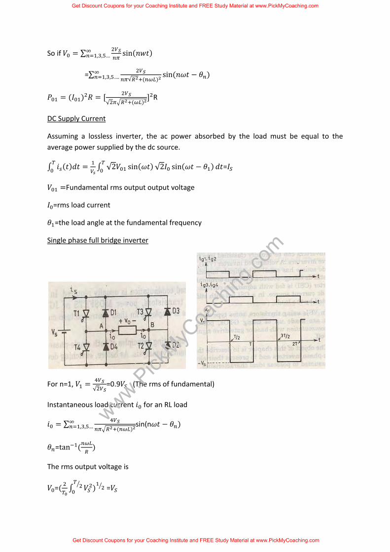
Single phase full bridge inverter
For n=1, 𝑉1 =4𝑉𝑆
√2𝑉𝑆=0.9𝑉𝑆 (The rms of fundamental)
Instantaneous load current 𝑖0 for an RL load
𝑖0 = ∑4𝑉𝑆
𝑛𝜋√𝑅2+(𝑛𝜔𝐿)2
∞𝑛=1,3,5… sin(n𝜔𝑡 − 𝜃𝑛)
𝜃𝑛=tan−1(𝑛𝜔𝐿
𝑅)
The rms output voltage is
𝑉0=(2
𝑇0∫ 𝑉𝑆
2𝑇
2⁄
0)
12⁄ =𝑉𝑆
Get Discount Coupons for your Coaching Institute and FREE Study Material at www.PickMyCoaching.com
Get Discount Coupons for your Coaching Institute and FREE Study Material at www.PickMyCoaching.com
www.Pick
MyCoa
ching
.com

The instantaneous output voltage in a fourier series
𝑣0 = ∑4𝑉𝑆
𝑛𝜋
∞
𝑛=1,3,5…
sin (𝑛𝜔𝑡)
Single phase bridge inverter
INVERTER
Inverters are of the two types
1) VSI
2) CSI
Pulse width model
The VSI can be further divided into general 3 categories:
1.Pulse width modulated inverters
2.Square wave inverters
3.Single phase inverter with voltage cancellation
Get Discount Coupons for your Coaching Institute and FREE Study Material at www.PickMyCoaching.com
Get Discount Coupons for your Coaching Institute and FREE Study Material at www.PickMyCoaching.com
www.Pick
MyCoa
ching
.com

Pulse width modulated inverters
The input dc voltage is of constant magnitude . The diode rectifier is used to rectify the line
voltage.The inverter control the magnitude and frequency of the ac output voltage.
This is achieved by PWM technique of inverter switches and this is called PWM inverters.
The sinusoidal PWM technique is one of the PWM technique to shape the output voltage to
as close as sinusoidal output.
Basic concepts of switch mode inverter
Get Discount Coupons for your Coaching Institute and FREE Study Material at www.PickMyCoaching.com
Get Discount Coupons for your Coaching Institute and FREE Study Material at www.PickMyCoaching.com
www.Pick
MyCoa
ching
.com
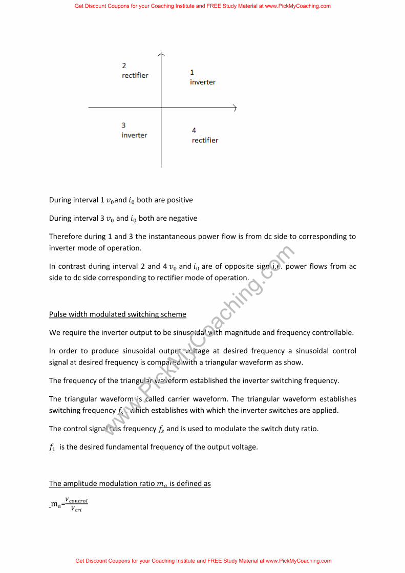
During interval 1 𝑣0and 𝑖0 both are positive
During interval 3 𝑣0 and 𝑖0 both are negative
Therefore during 1 and 3 the instantaneous power flow is from dc side to corresponding to
inverter mode of operation.
In contrast during interval 2 and 4 𝑣0 and 𝑖0 are of opposite sign i.e. power flows from ac
side to dc side corresponding to rectifier mode of operation.
Pulse width modulated switching scheme
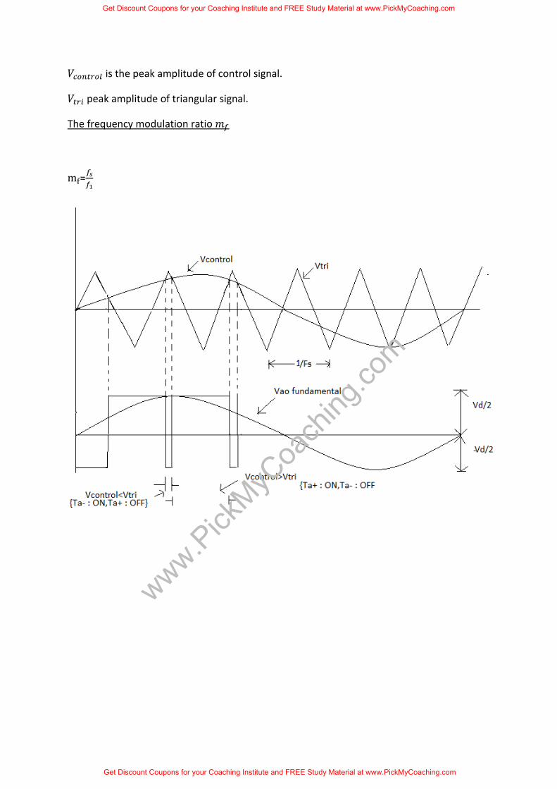
We require the inverter output to be sinusoidal with magnitude and frequency controllable.
In order to produce sinusoidal output voltage at desired frequency a sinusoidal control
signal at desired frequency is compared with a triangular waveform as show.
The frequency of the triangular waveform established the inverter switching frequency.
The triangular waveform is called carrier waveform. The triangular waveform establishes
switching frequency 𝑓𝑠 , which establishes with which the inverter switches are applied.
The control signal has frequency 𝑓𝑠 and is used to modulate the switch duty ratio.
𝑓1 is the desired fundamental frequency of the output voltage.
The amplitude modulation ratio 𝑚𝑎 is defined as
ma=𝑉𝑐𝑜𝑛𝑡𝑟𝑜𝑙
𝑉𝑡𝑟𝑖
Get Discount Coupons for your Coaching Institute and FREE Study Material at www.PickMyCoaching.com
Get Discount Coupons for your Coaching Institute and FREE Study Material at www.PickMyCoaching.com
www.Pick
MyCoa
ching
.com
𝑉𝑐𝑜𝑛𝑡𝑟𝑜𝑙 is the peak amplitude of control signal.
𝑉𝑡𝑟𝑖 peak amplitude of triangular signal.
The frequency modulation ratio 𝑚𝑓
mf=𝑓𝑠
𝑓1
Get Discount Coupons for your Coaching Institute and FREE Study Material at www.PickMyCoaching.com
Get Discount Coupons for your Coaching Institute and FREE Study Material at www.PickMyCoaching.com
www.Pick
MyCoa
ching
.com

When 𝑉𝑐𝑜𝑛𝑡𝑟𝑜𝑙 > 𝑉𝑡𝑟𝑖 𝑇𝐴+ is ON 𝑉𝐴𝑂 =
1
2𝑉𝑑
𝑉𝑐𝑜𝑛𝑡𝑟𝑜𝑙 < 𝑉𝑡𝑟𝑖 𝑇𝐴− is ON 𝑉𝐴𝑂 =
1
2𝑉𝑑
So the following inferences can be drawn
The peak amplitude of fundamental frequency is matimes 1
2𝑉𝑑
𝑉𝐴𝑂=𝑚𝑎
𝑉𝑑2
𝑉𝐴𝑂=𝑉𝑐𝑜𝑛𝑡𝑟𝑜𝑙
𝑉𝑡𝑟𝑖∗
𝑉𝑑
2 𝑉𝑐𝑜𝑛𝑡𝑟𝑜𝑙 ≤ �̂�𝑡𝑟𝑖
The foregoing arguments shown why Vcontrolis chosen to be sinusoidal to provide sinusoidal
output voltage with fewer harmonics
Let the Vcontrol vary sinusoidal with frequency f1,which is the desired frequency of the
inverter output voltage.
Let Vcontrol=V̂controlsin𝜔1t
V̂control ≤ V̂tri
Get Discount Coupons for your Coaching Institute and FREE Study Material at www.PickMyCoaching.com
Get Discount Coupons for your Coaching Institute and FREE Study Material at www.PickMyCoaching.com
www.Pick
MyCoa
ching
.com

�̂�𝑡𝑟𝑖
𝑡1=
𝑉𝑡𝑟𝑖𝑇𝑠
4⁄
At t=𝑡1 , 𝑣𝑡𝑟𝑖=𝑣𝑐𝑜𝑛𝑡𝑟𝑜𝑙
So 𝑣𝑐𝑜𝑛𝑡𝑟𝑜𝑙
𝑡1=
𝑉𝑡𝑟𝑖𝑇𝑠
4⁄
𝑡1=�̂�𝑐𝑜𝑛𝑡𝑟𝑜𝑙
𝑉𝑡𝑟𝑖*
𝑇𝑆
4
𝑇𝑜𝑛=2𝑡1+𝑇𝑆
2
𝐷1=𝑇𝑜𝑛
𝑇𝑠=
2𝑡1+𝑇𝑆2
2
=1
2+
2𝑡1
𝑇𝑠
𝐷1=1
2+
1
2(�̂�𝑐𝑜𝑛𝑡𝑟𝑜𝑙
𝑉𝑡𝑟𝑖)
Three phase inverter
When three single-phase inverters are connected in parallel a three phase inverter is
formed.
The gating signal has to be displaced by 1200 with respect to each other so as achieve three
phase balanced voltages.
A 3-phase output can be achieved from a configuration of six transistors and six diodes.
Get Discount Coupons for your Coaching Institute and FREE Study Material at www.PickMyCoaching.com
Get Discount Coupons for your Coaching Institute and FREE Study Material at www.PickMyCoaching.com
www.Pick
MyCoa
ching
.com

Two type of control signal can be applied to transistors, they are such as 1800 or 1200
conduction.
180-degree conduction
When 𝑄1 is switched on, terminal a is connected to the positive terminal of dc input voltage.
When 𝑄4 is switched on terminal a is brought to negative terminal of the dc source.
There are 6 modes of operation is a cycle and the duration of each mode is 600.
The conduction sequence of transistors is 123,234,345,456,561,612. The gating signals are
shifted from each other by 600 to get 3-𝜑 balanced voltages.
Switching states for the three phase voltage inverters
Get Discount Coupons for your Coaching Institute and FREE Study Material at www.PickMyCoaching.com
Get Discount Coupons for your Coaching Institute and FREE Study Material at www.PickMyCoaching.com
www.Pick
MyCoa
ching
.com

Get Discount Coupons for your Coaching Institute and FREE Study Material at www.PickMyCoaching.com
Get Discount Coupons for your Coaching Institute and FREE Study Material at www.PickMyCoaching.com
www.Pick
MyCoa
ching
.com

𝑉𝑅𝑁 𝑉𝑌𝑁 𝑉𝐵𝑁 𝑉𝑅𝑌 𝑉𝑌𝐵 𝑉𝐵𝑅 𝑉1
𝑉
3
−2𝑉
3
𝑉
3
𝑉𝑎𝑐 −𝑉𝑑𝑐 0 2
√3(3300)
2𝑉
3
−𝑉
3
−𝑉
3
𝑉𝑑𝑐 0 −𝑉𝑑𝑐 2
√3(300)
𝑉
3
𝑉
3
−2𝑉
3
0 V -V 2
√3(900)
−𝑉
3
2𝑉
3
−𝑉
3
-V V 0 2
√3(1500)
−2𝑉
3
𝑉
3
𝑉
3
-V 0 0 2
√3(2100)
−𝑉
3
−𝑉
3
2𝑉
3
0 -V 0 2
√3(2700)
Fourier analysis
If we go for harmonic analysis 𝑉𝑅𝑌=∑
4𝑉
𝑛𝜋𝑠𝑖𝑛
𝑛𝜋
3sin 𝑛(𝜔𝑡+𝜋
6⁄ )∞𝑛=1,3,5…
5,6,1
6,1,2
1,2,3 2,3,4
3,4,5
4,5,6
Get Discount Coupons for your Coaching Institute and FREE Study Material at www.PickMyCoaching.com
Get Discount Coupons for your Coaching Institute and FREE Study Material at www.PickMyCoaching.com
www.Pick
MyCoa
ching
.com

𝑉𝑌𝐵=∑
4𝑉𝑆𝑛𝜋
𝑠𝑖𝑛𝑛𝜋3
sin 𝑛(𝜔𝑡−𝜋2⁄ )∞
𝑛=1,3,5…
𝑉𝐵𝑅=∑
4𝑉𝑆𝑛𝜋
𝑠𝑖𝑛𝑛𝜋3
sin 𝑛(𝜔𝑡−𝜋6⁄ )∞
𝑛=1,3,5…
All even harmonics are zero all triple n harmonics are zero.
The rms nth component of the line voltage is
=4𝑉
√2𝑛𝜋sin
𝑛𝜋
3=
4𝑉
√2𝜋sin(60)
For n=1
=0.7797𝑉𝑆
Three phase 1200mode VSI
The circuit diagram is same as that for 1800 mode of conduction.
Here each thyristor conducts for 1200.There are 6 steps each of 600 duration, for
completing one cycle of ac output voltage.
6,1
1,2
2,3 3,4
4,5
5,6
Get Discount Coupons for your Coaching Institute and FREE Study Material at www.PickMyCoaching.com
Get Discount Coupons for your Coaching Institute and FREE Study Material at www.PickMyCoaching.com
www.Pick
MyCoa
ching
.com
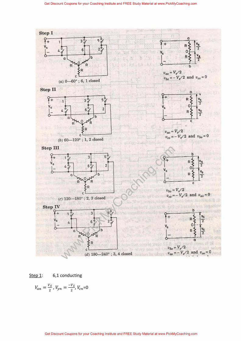
Step 1: 6,1 conducting
𝑉𝑎𝑛 =𝑉𝑆
2 , 𝑉𝑦𝑛 =
−𝑉𝑆
2, 𝑉𝑐𝑛=0
Get Discount Coupons for your Coaching Institute and FREE Study Material at www.PickMyCoaching.com
Get Discount Coupons for your Coaching Institute and FREE Study Material at www.PickMyCoaching.com
www.Pick
MyCoa
ching
.com

Step 2: 1,2 conducting
𝑉𝑎𝑛 =𝑉𝑆
2 , 𝑉𝑏𝑛 = 0, 𝑉𝑐𝑛=
−𝑉𝑆
2
Step 3: 2,3 conducting
𝑉𝑎𝑛 =0, 𝑉𝑏𝑛=𝑉𝑆
2, 𝑉𝑐𝑛=
−𝑉𝑆
2
Step 4: 3,4 conducting
𝑉𝑎𝑛 = −𝑉𝑆
2, 𝑉𝑏𝑛=
𝑉𝑆
2, 𝑉𝑐𝑛=0
Step 5: 4,5 conducting
𝑉𝑎𝑛== −𝑉𝑆
2, 𝑉𝑦𝑛 = 0, 𝑉𝑏𝑛 =
𝑉𝑆
2
Step 6: 5,6 conducting
𝑉𝑎𝑛=0, 𝑉𝑏𝑛 =−𝑉𝑆
2, 𝑉𝑐𝑛=
𝑉𝑆
2
1200 conduction mode
Step Thyristor conducting
𝑉𝑅𝑛 𝑉𝑌𝑛 𝑉𝐵𝑛 V→
1 6,1 Vs2
⁄ −𝑉𝑠
2⁄ 0 √3VS
2(−300)
2 1,2 𝑉𝑠2
⁄ 0 −𝑉𝑠2
⁄ √3VS
2(300)
3 2,3 0 𝑉𝑠2
⁄ −𝑉𝑠2
⁄ √3VS
2(900)
4 3,4 −𝑉𝑠2
⁄ 𝑉𝑠2
⁄ 0 √3VS
2(1500)
5 4,5 −𝑉𝑠2
⁄ 0 𝑉𝑠2
⁄ √3V
2(2100)
6 5,6 0 −𝑉𝑠2
⁄ 𝑉𝑠2
⁄ √3V
2(−300)
Get Discount Coupons for your Coaching Institute and FREE Study Material at www.PickMyCoaching.com
Get Discount Coupons for your Coaching Institute and FREE Study Material at www.PickMyCoaching.com
www.Pick
MyCoa
ching
.com

Get Discount Coupons for your Coaching Institute and FREE Study Material at www.PickMyCoaching.com
Get Discount Coupons for your Coaching Institute and FREE Study Material at www.PickMyCoaching.com
www.Pick
MyCoa
ching
.com