Lecture 2.2: Energy Band View of the MOSFET
24
Essentials of MOSFETs Unit 2: Essential Physics of the MOSFET Lecture 2.2: Energy Band View of the MOSFET Mark Lundstrom [email protected] Electrical and Computer Engineering Purdue University West Lafayette, Indiana USA 1 Lundstrom: 2018
Transcript of Lecture 2.2: Energy Band View of the MOSFET

Essentials of MOSFETs
Unit 2: Essential Physics of the MOSFET
Lecture 2.2: Energy Band View of the MOSFET
Mark Lundstrom
[email protected] Electrical and Computer Engineering
Purdue University West Lafayette, Indiana USA
1 Lundstrom: 2018
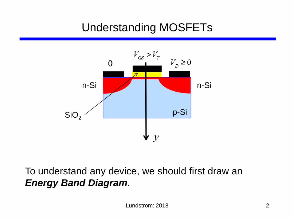
Understanding MOSFETs
p-Si
n-Si n-Si
To understand any device, we should first draw an Energy Band Diagram.
Lundstrom: 2018 2
SiO2
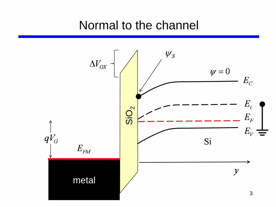
Normal to the channel
3
metal 3
SiO
2
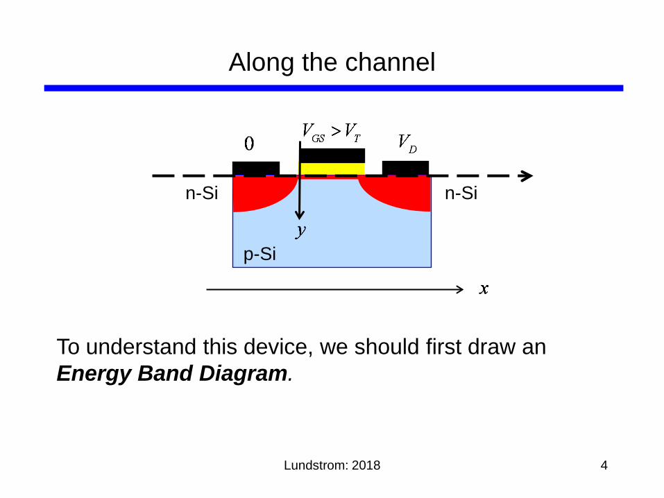
Along the channel
p-Si
n-Si n-Si
To understand this device, we should first draw an Energy Band Diagram.
Lundstrom: 2018 4

Equilibrium E-band diagram
p-Si
n-Si n-Si
source channel drain Lundstrom: 2018
5

Three separate semiconductors
source channel drain
1) Equilibrium: Fermi level is constant
2) Changes in electrostatic potential, change the electron’s energy.
Lundstrom: 2018 6

Putting the three pieces together
source channel drain
Lundstrom: 2018 7
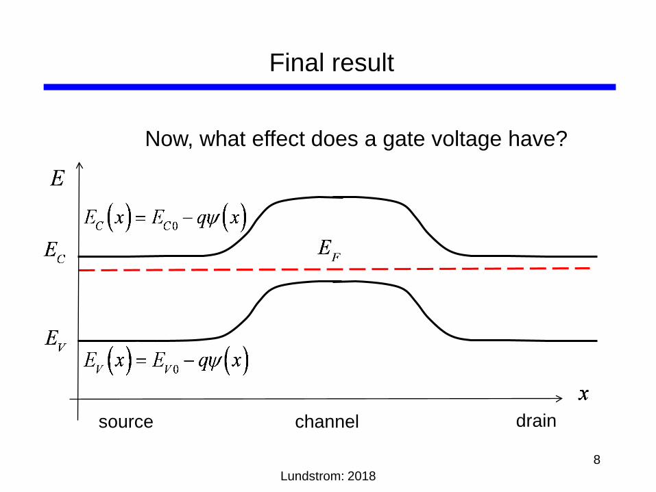
Final result
source channel drain
Now, what effect does a gate voltage have?
Lundstrom: 2018 8

Equilibrium energy band diagram
p-Si
n-Si n-Si
A positive gate voltage will increase the electrostatic potential in the channel and therefore lower the electron energy in the channel.
Lundstrom: 2018 9

N-channel MOSFET: only electrons
source channel drain
Now, what effect does a gate voltage have?
Lundstrom: 2018 10
In the following slides, we will show only the conduction band.

The transistor as a barrier controlled device
Lundstrom: 2018
source drain channel
low gate voltage
VD = VS = 0
11

Examine effect of gate voltage first
low gate voltage
high gate voltage
Lundstrom: 2018 12

Now add a small drain voltage
What if we apply a small positive voltage to the drain?
1) The Fermi level in the drain is lowered.
2) The conduction band is
lowered too, but the electron density stays the same.
Lundstrom: 2018
constant electric field substantial electron density
13

Now increase the drain voltage
Lundstrom: 2018
high gate voltage
source high drain voltage
14
ON-state

Now remove the gate voltage
Lundstrom: 2018
low gate voltage
source drain channel
high drain voltage
15
OFF-state

How transistors work
2007 N-MOSFET
(Courtesy, Shuji Ikeda, ATDF, Dec. 2007)
Lundstrom: 2018 16

DIBL
Lundstrom: 2018
transfer characteristics:
17
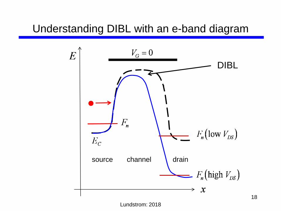
Understanding DIBL with an e-band diagram
Lundstrom: 2018
source drain channel
DIBL
18

2D energy band diagrams
p-Si
n-Si n-Si
We have been discussing energy band diagrams from the source to the drain along the top of the Si, but more generally, we should look at the 2D energy band diagram.
Lundstrom: 2018 19

2D energy band diagram on n-MOSFET
Lundstrom: 2018
(a)
(b)
(c)
(d)
S.M. Sze, Physics of Semiconductor Devices, 1981.
a) device b) equilibrium (flat band) c) equilibrium (S > 0) d) non-equilibrium with VG and VD > 0
applied FN 20

Essential physics of a transistor
Lundstrom: 2018
A MOSFET (and most transistors) are barrier-controlled devices.
21

Limits to barrier control: quantum tunneling
from M. Luisier, ETH Zurich / Purdue
1) 2)
3) 4)
Lundstrom: 2018 22

Summary
1) Energy band diagrams provide a qualitative understanding of how MOSFETs operate.
23
2) MOSFETs are barrier controlled devices – the drain current is controlled by the height of an energy barrier between the source and channel.
Lundstrom: 2018
3) In a well-designed transistor, the height of the energy barrier is strongly controlled by the gate voltage and weakly by the drain voltage (DIBL).

Next topic:
Lundstrom: 2018 24
In the next lecture, we will discuss traditional MOSFET theory, which describes the IV characteristics with simple analytical expressions.