Lecture 2 – Combinational Circuits and Verilog
64
Lecture 2 – Combinational Circuits and Verilog CSE P567
Transcript of Lecture 2 – Combinational Circuits and Verilog
Lecture 2 – Combinational Circuits and Verilog
CSE P567
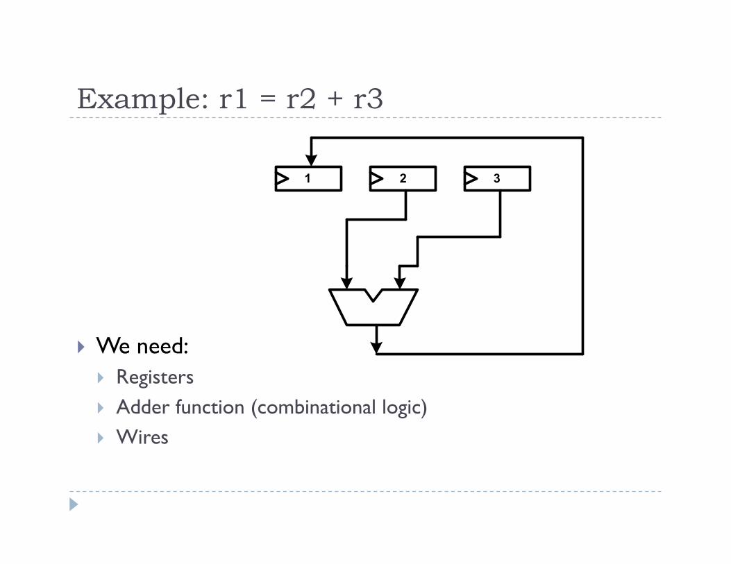
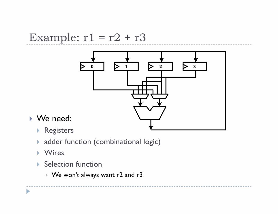
Example: r1 = r2 + r3
We need: Registers Adder function (combinational logic) Wires
Example: r1 = r2 + r3
We need: Registers adder function (combinational logic) Wires Selection function
We won’t always want r2 and r3
Combinational Logic Functions with no state Output is a function of the inputs only – no history
add subtract multiply count-ones FSM next state function
All computation is done in binary Primitive circuit values are on/off, Vdd/GND, current/no
current
Review: Binary Encoding of Numbers Unsigned numbers
bn-12n-1 + bn-22n-2 + . . . + b020
2s complement encoding of signed numbers -bn-12n-1 + bn-22n-2 + . . . + b020
Same adder works for both unsigned and signed numbers
To negate a number, invert all bits and add 1 As slow as add in worst case

Binary Addition Simple addition algorithm works:
0 1 1 0 +6 1 1 0 1 -3 ---------
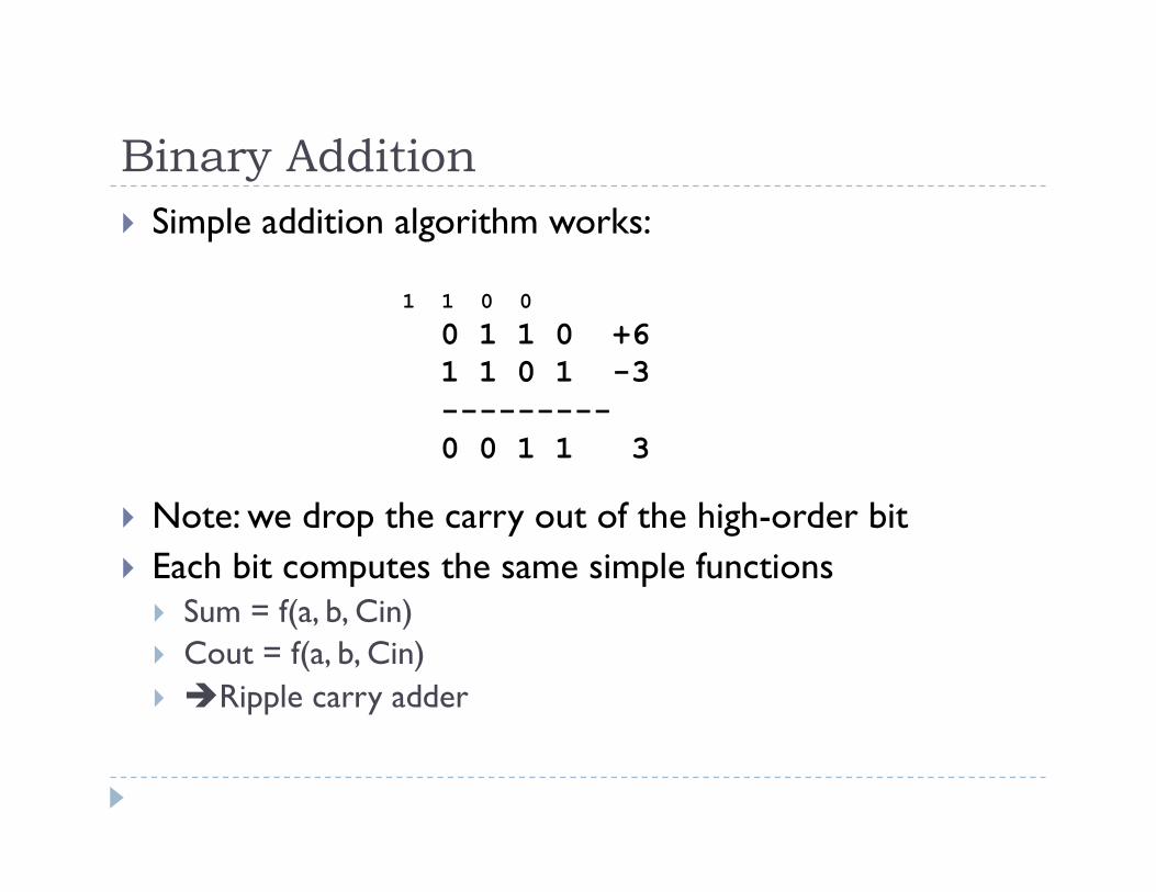
Binary Addition Simple addition algorithm works:
Note: we drop the carry out of the high-order bit Each bit computes the same simple functions
Sum = f(a, b, Cin) Cout = f(a, b, Cin) Ripple carry adder
1 1 0 0
0 1 1 0 +6 1 1 0 1 -3 --------- 0 0 1 1 3
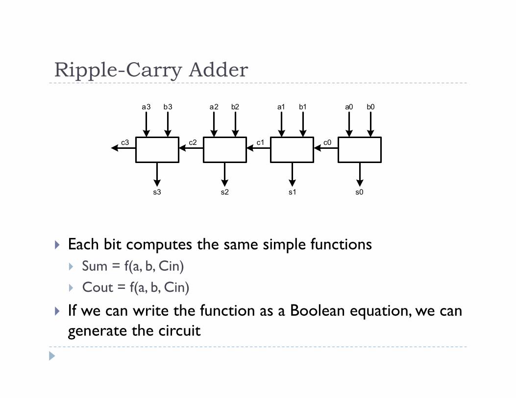
Ripple-Carry Adder
Each bit computes the same simple functions Sum = f(a, b, Cin) Cout = f(a, b, Cin)
If we can write the function as a Boolean equation, we can generate the circuit
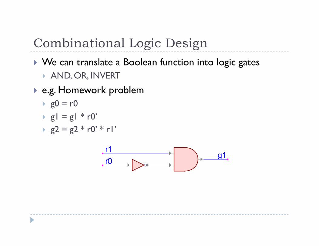
Combinational Logic Design We can translate a Boolean function into logic gates
AND, OR, INVERT
e.g. Homework problem g0 = r0 g1 = g1 * r0’ g2 = g2 * r0’ * r1’
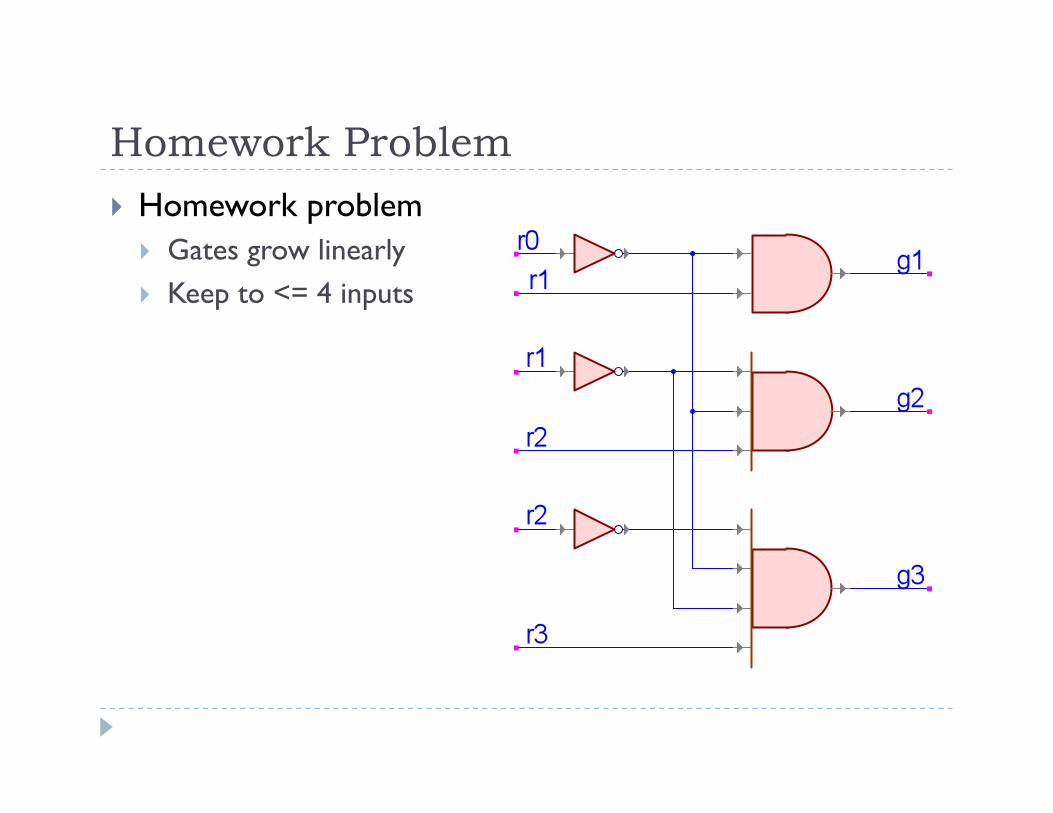
Homework Problem Homework problem
Gates grow linearly Keep to <= 4 inputs
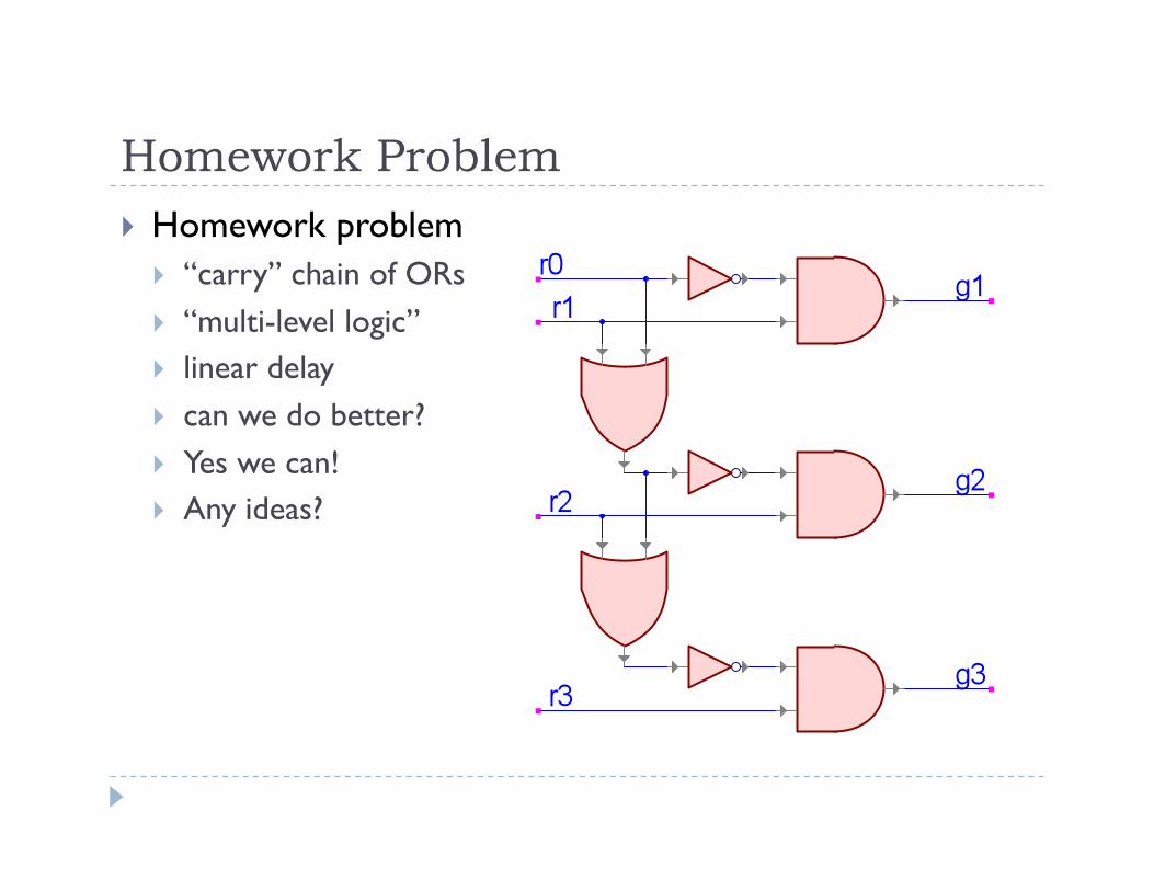
Homework Problem Homework problem
“carry” chain of ORs “multi-level logic” linear delay can we do better? Yes we can! Any ideas?
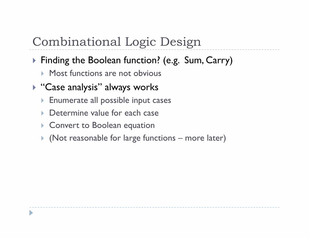
Combinational Logic Design Finding the Boolean function? (e.g. Sum, Carry)
Most functions are not obvious
“Case analysis” always works Enumerate all possible input cases Determine value for each case Convert to Boolean equation (Not reasonable for large functions – more later)
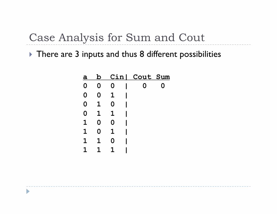
Case Analysis for Sum and Cout There are 3 inputs and thus 8 different possibilities
a b Cin| Cout Sum 0 0 0 | 0 0 0 0 1 | 0 1 0 | 0 1 1 | 1 0 0 | 1 0 1 | 1 1 0 | 1 1 1 |
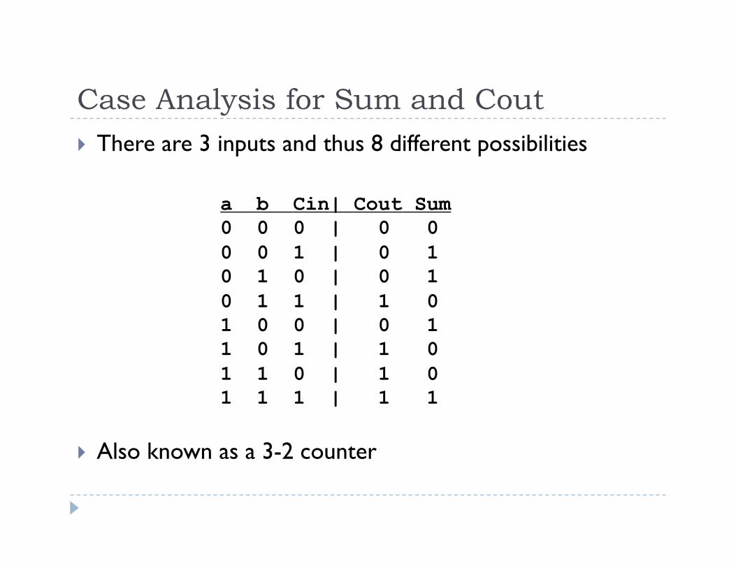
Case Analysis for Sum and Cout There are 3 inputs and thus 8 different possibilities
Also known as a 3-2 counter
a b Cin| Cout Sum 0 0 0 | 0 0 0 0 1 | 0 1 0 1 0 | 0 1 0 1 1 | 1 0 1 0 0 | 0 1 1 0 1 | 1 0 1 1 0 | 1 0 1 1 1 | 1 1
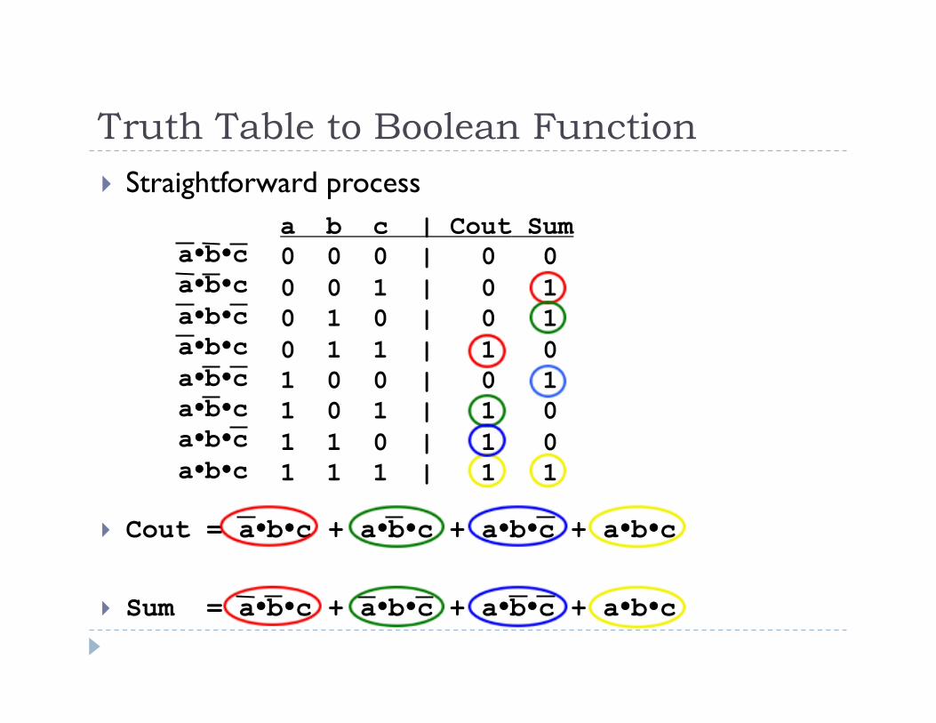
Truth Table to Boolean Function Straightforward process
Cout = abc + abc + abc + abc
Sum = abc + abc + abc + abc
a b c | Cout Sum 0 0 0 | 0 0 0 0 1 | 0 1 0 1 0 | 0 1 0 1 1 | 1 0 1 0 0 | 0 1 1 0 1 | 1 0 1 1 0 | 1 0 1 1 1 | 1 1
abc abc abc abc abc abc abc abc
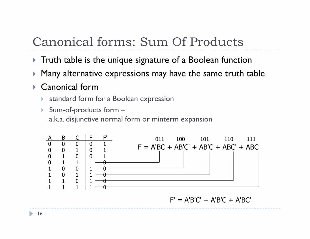
16
A B C F F' 0 0 0 0 1 0 0 1 0 1 0 1 0 0 1 0 1 1 1 0 1 0 0 1 0 1 0 1 1 0 1 1 0 1 0 1 1 1 1 0
011 100 101 110 111 F = A'BC + AB'C' + AB'C + ABC' + ABC
F' = A'B'C' + A'B'C + A'BC'
Canonical forms: Sum Of Products Truth table is the unique signature of a Boolean function Many alternative expressions may have the same truth table Canonical form
standard form for a Boolean expression Sum-of-products form –
a.k.a. disjunctive normal form or minterm expansion
17
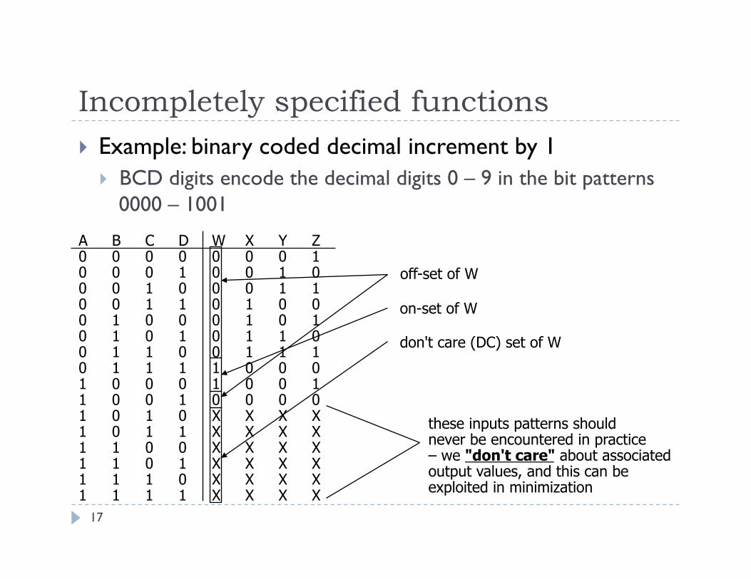
A B C D W X Y Z 0 0 0 0 0 0 0 1 0 0 0 1 0 0 1 0 0 0 1 0 0 0 1 1 0 0 1 1 0 1 0 0 0 1 0 0 0 1 0 1 0 1 0 1 0 1 1 0 0 1 1 0 0 1 1 1 0 1 1 1 1 0 0 0 1 0 0 0 1 0 0 1 1 0 0 1 0 0 0 0 1 0 1 0 X X X X 1 0 1 1 X X X X 1 1 0 0 X X X X 1 1 0 1 X X X X 1 1 1 0 X X X X 1 1 1 1 X X X X
off-set of W
these inputs patterns should never be encountered in practice – we "don't care" about associated output values, and this can be exploited in minimization
don't care (DC) set of W
on-set of W
Incompletely specified functions Example: binary coded decimal increment by 1
BCD digits encode the decimal digits 0 – 9 in the bit patterns 0000 – 1001
18
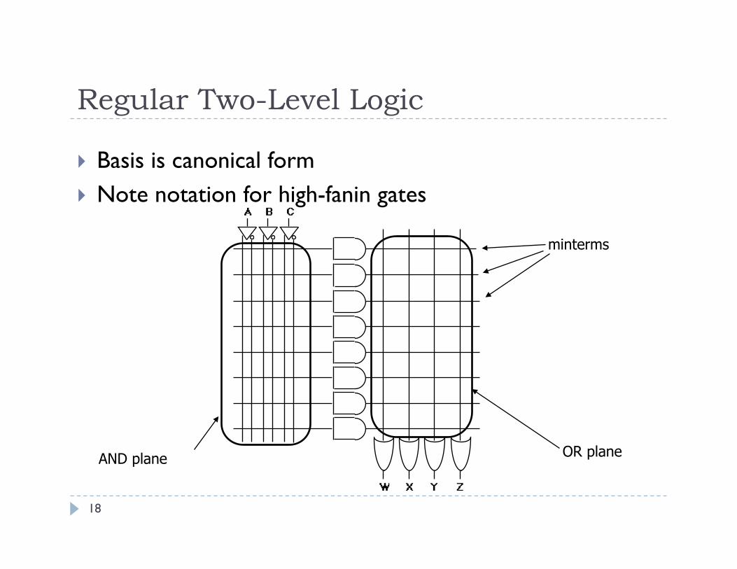
minterms
AND plane OR plane
Regular Two-Level Logic
Basis is canonical form Note notation for high-fanin gates
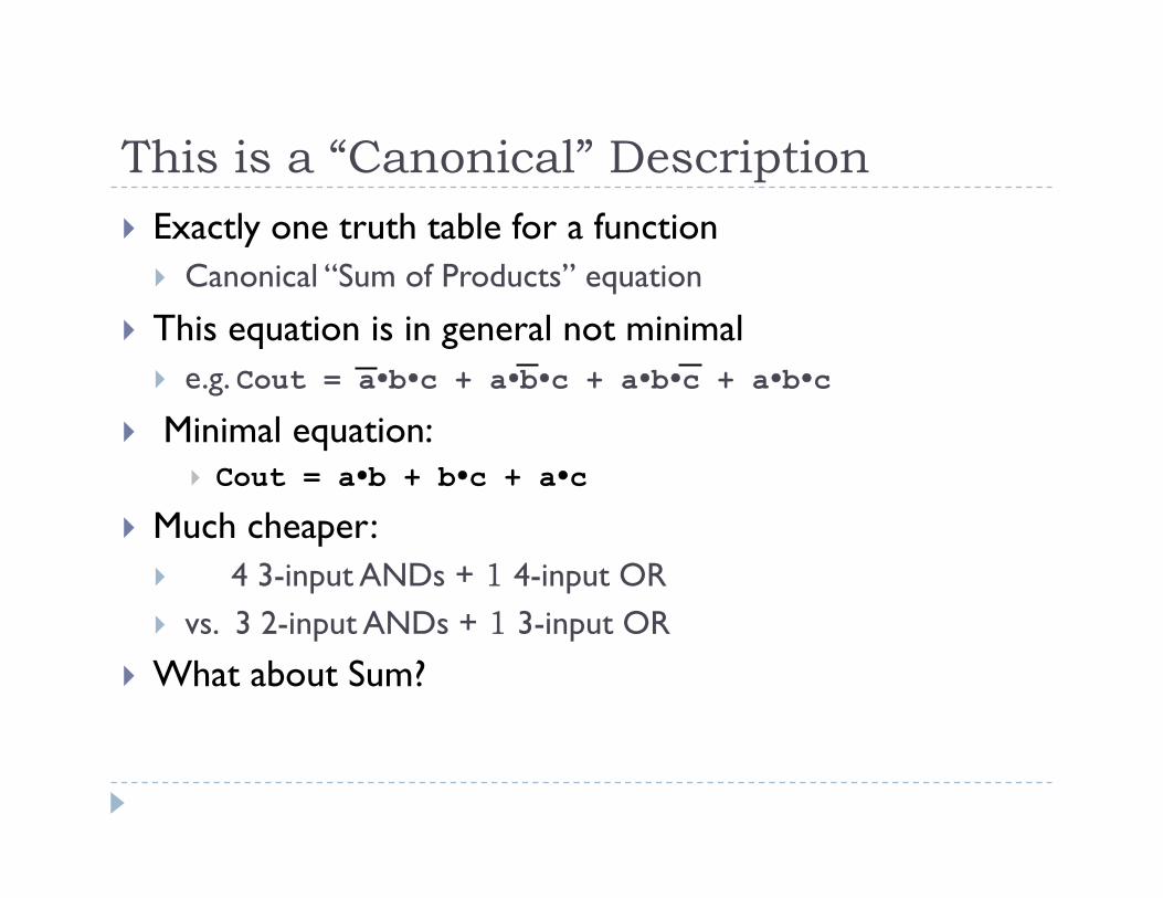
This is a “Canonical” Description Exactly one truth table for a function
Canonical “Sum of Products” equation
This equation is in general not minimal e.g. Cout = abc + abc + abc + abc
Minimal equation: Cout = ab + bc + ac
Much cheaper: 4 3-input ANDs + 1 4-input OR vs. 3 2-input ANDs + 1 3-input OR
What about Sum?
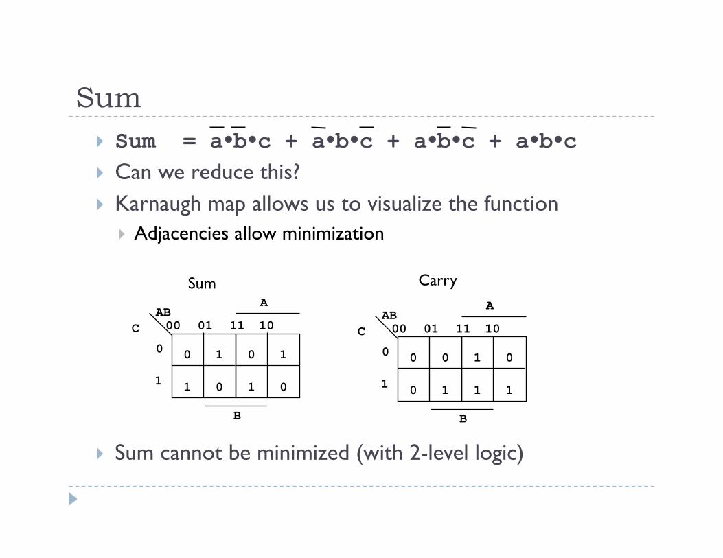
Sum Sum = abc + abc + abc + abc Can we reduce this? Karnaugh map allows us to visualize the function
Adjacencies allow minimization
Sum cannot be minimized (with 2-level logic)
0 1 0 1
1 0 1 0
0
1
AB A
00 01 11 10 C
B
0 0 1 0
0 1 1 1
0
1
AB A
00 01 11 10 C
B
Sum Carry
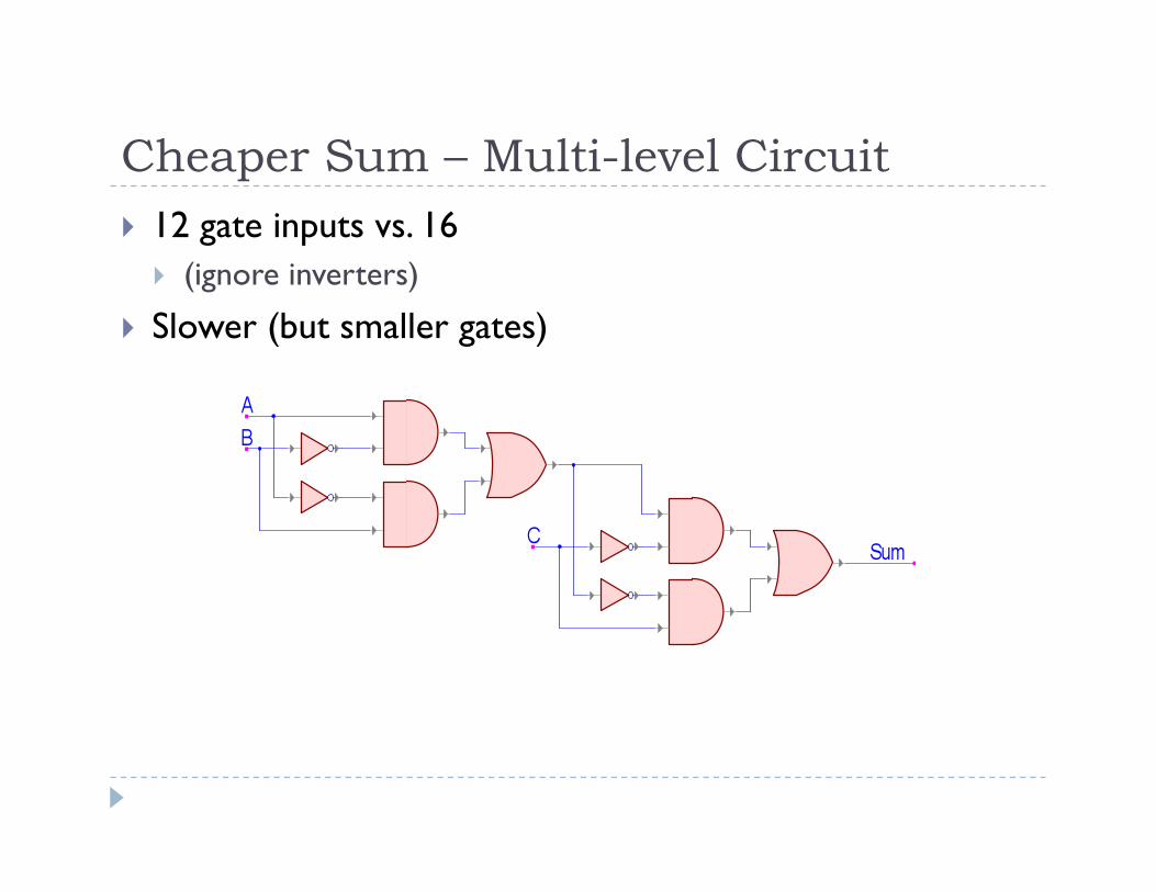
Cheaper Sum – Multi-level Circuit 12 gate inputs vs. 16
(ignore inverters)
Slower (but smaller gates)
22
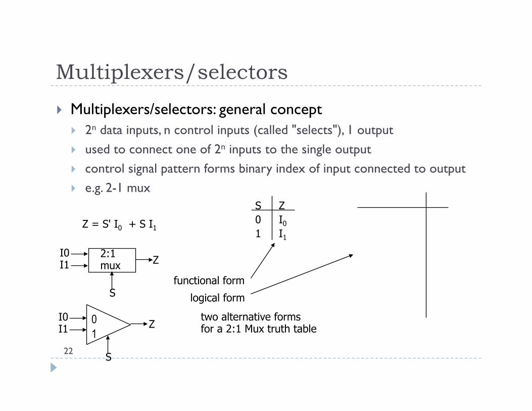
two alternative forms for a 2:1 Mux truth table
functional form
logical form
S Z 0 I0 1 I1
Z = S' I0 + S I1
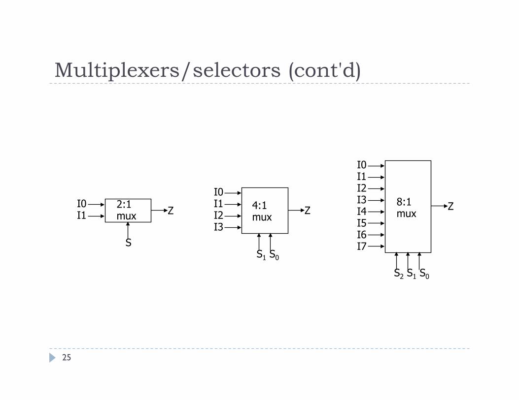
Multiplexers/selectors
Multiplexers/selectors: general concept 2n data inputs, n control inputs (called "selects"), 1 output used to connect one of 2n inputs to the single output control signal pattern forms binary index of input connected to output e.g. 2-1 mux
I0 I1
S
2:1 mux Z
I0 I1
S
Z 0 1
23
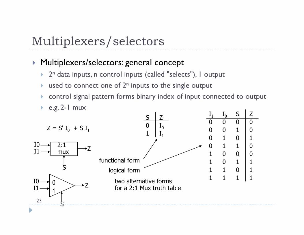
two alternative forms for a 2:1 Mux truth table
functional form
logical form
S Z 0 I0 1 I1
I1 I0 S Z 0 0 0 0 0 0 1 0 0 1 0 1 0 1 1 0 1 0 0 0 1 0 1 1 1 1 0 1 1 1 1 1
Z = S' I0 + S I1
Multiplexers/selectors
Multiplexers/selectors: general concept 2n data inputs, n control inputs (called "selects"), 1 output used to connect one of 2n inputs to the single output control signal pattern forms binary index of input connected to output e.g. 2-1 mux
I0 I1
S
2:1 mux Z
I0 I1
S
Z 0 1
24
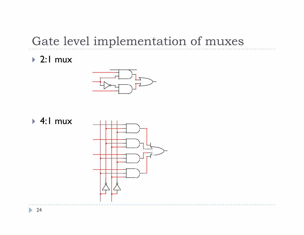
Gate level implementation of muxes 2:1 mux
4:1 mux
25
I0 I1 I2 I3 I4 I5 I6 I7
S2 S1 S0
8:1 mux
Z I0 I1 I2 I3
S1 S0
4:1 mux
Z I0 I1
S
2:1 mux Z
Multiplexers/selectors (cont'd)
26
alternative implementation
S2
Z
S1 S0
4:1 mux
2:1 mux
2:1 mux
2:1 mux
2:1 mux
I4 I5
I2 I3
I0 I1
I6 I7
8:1 mux
Z
I0 I1 I2 I3
S0
I4 I5 I6 I7
S2 S1
4:1 mux
4:1 mux
2:1 mux
8:1 mux
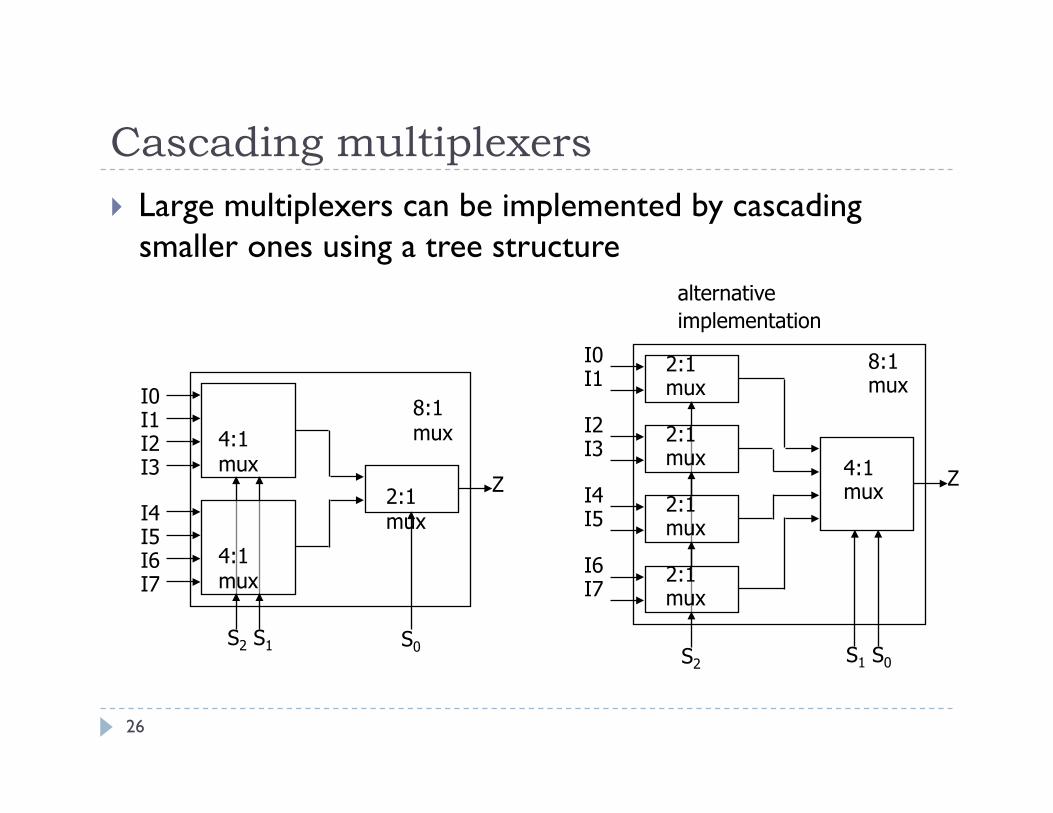
Cascading multiplexers Large multiplexers can be implemented by cascading
smaller ones using a tree structure
27
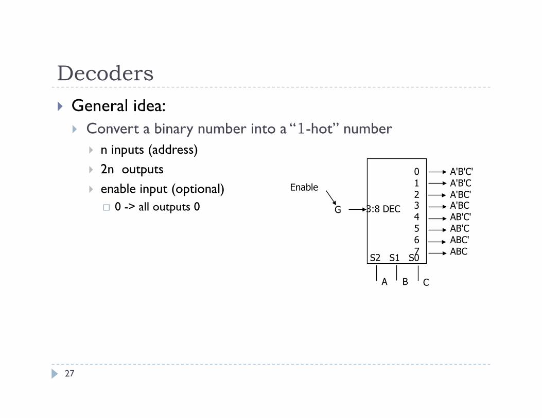
C A B
0 A'B'C' 1 A'B'C 2 A'BC' 3 A'BC 4 AB'C' 5 AB'C 6 ABC' 7 ABC
S2
3:8 DEC
S1 S0
G
Enable
Decoders General idea:
Convert a binary number into a “1-hot” number n inputs (address) 2n outputs enable input (optional)
0 -> all outputs 0
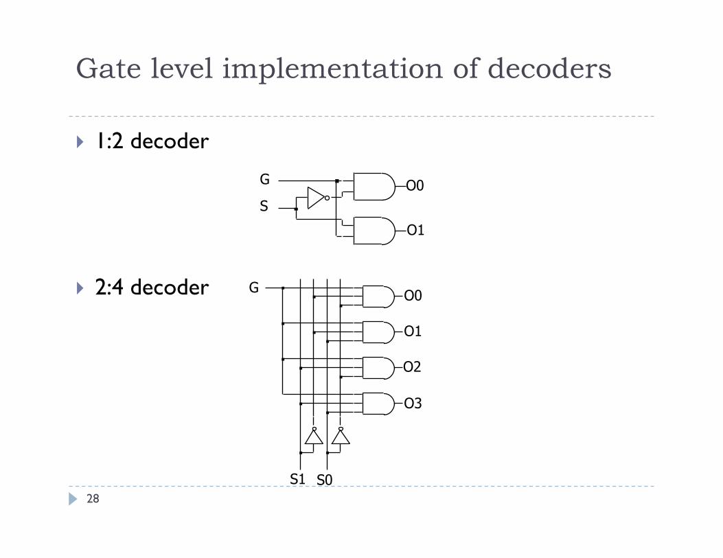
Gate level implementation of decoders
28
1:2 decoder
2:4 decoder
O0 G
S
O1
S1
O2
O3
O0 G
O1
S0
29
0 A'B'C'D'E' 1 2 3 4 5 6 7 S2
3:8 DEC
S1 S0
A B
0 1 2 3 S1
2:4 DEC
S0
F
0 1 2 A'BC'DE' 3 4 5 6 7 S2
3:8 DEC
S1 S0
E C D
0 AB'C'D'E' 1 2 3 4 5 6 7 AB'CDE
3:8 DEC
0 1 2 3 4 5 6 7 ABCDE
E C D
S2 S1 S0 S2
3:8 DEC
S1 S0
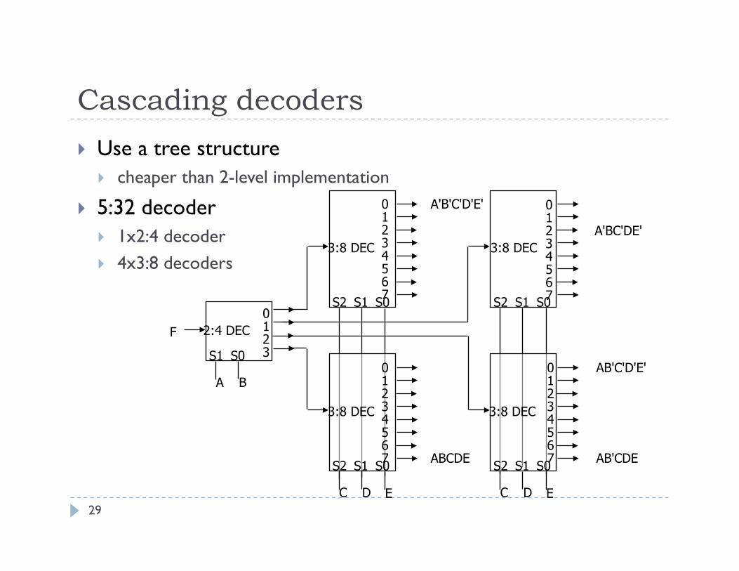
Cascading decoders
Use a tree structure cheaper than 2-level implementation
5:32 decoder 1x2:4 decoder 4x3:8 decoders
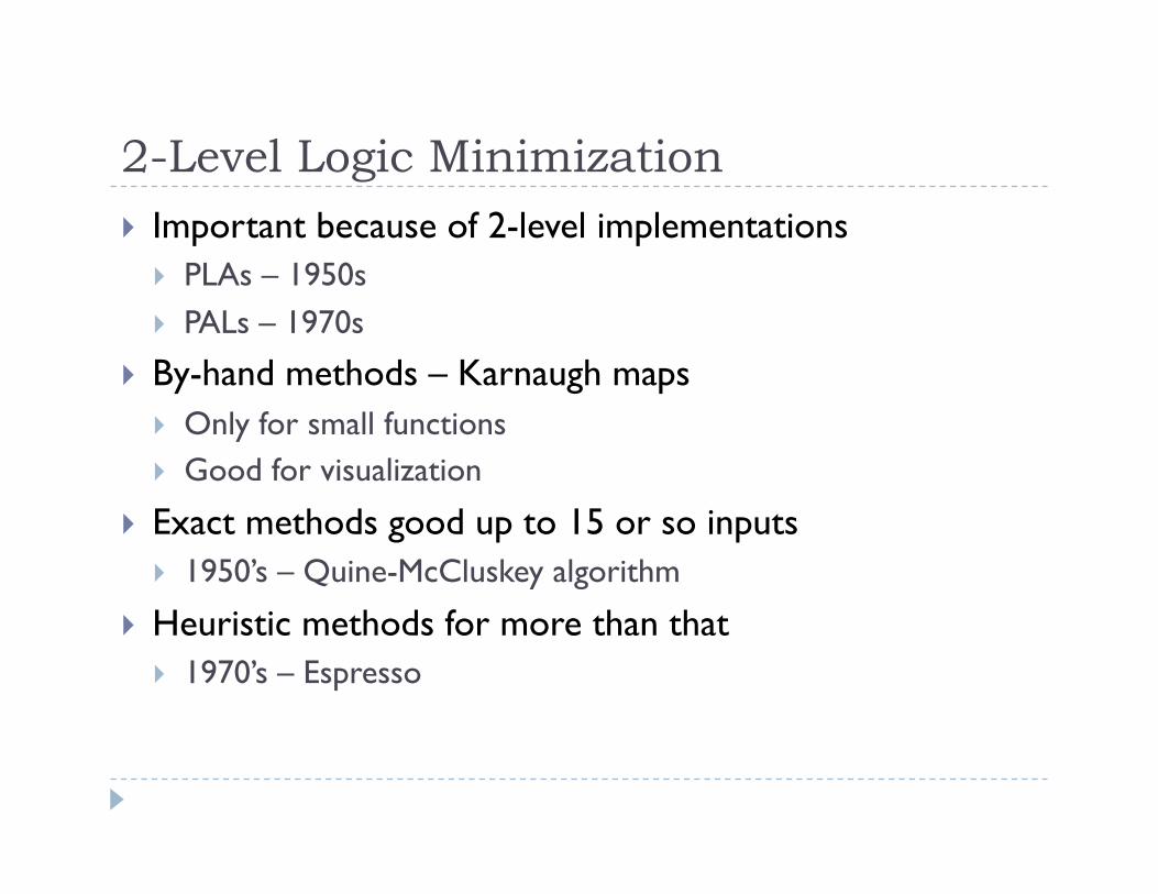
2-Level Logic Minimization Important because of 2-level implementations
PLAs – 1950s PALs – 1970s
By-hand methods – Karnaugh maps Only for small functions Good for visualization
Exact methods good up to 15 or so inputs 1950’s – Quine-McCluskey algorithm
Heuristic methods for more than that 1970’s – Espresso
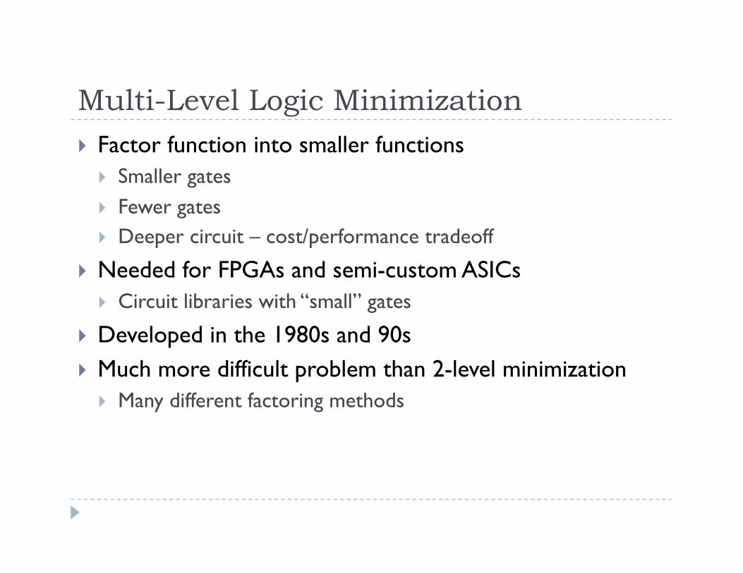
Multi-Level Logic Minimization Factor function into smaller functions
Smaller gates Fewer gates Deeper circuit – cost/performance tradeoff
Needed for FPGAs and semi-custom ASICs Circuit libraries with “small” gates
Developed in the 1980s and 90s Much more difficult problem than 2-level minimization
Many different factoring methods
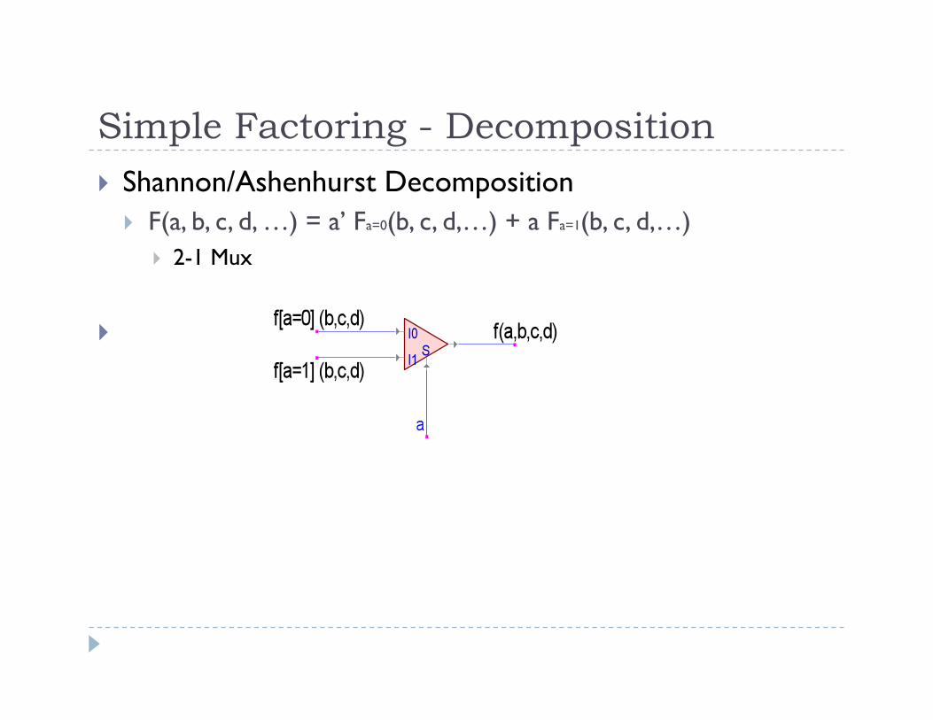
Simple Factoring - Decomposition Shannon/Ashenhurst Decomposition
F(a, b, c, d, …) = a’ Fa=0(b, c, d,…) + a Fa=1(b, c, d,…) 2-1 Mux
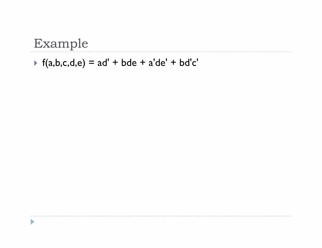
Example f(a,b,c,d,e) = ad' + bde + a'de' + bd'c'
Logic Synthesis Compiles HDL into gates 1. Elaboration – parse HDL program into standard form 2. Logic optimization – minimize cost/maximize
performance 3. Tech mapping – map optimized circuit to available
library components May require “re-synthesis”
4. Physical Re-Synthesis – transform circuit when placing and routing Process is unpredictable
Logic Synthesis Insulates us from the details
Like a C or Java compiler
But we need to understand the implications of what we write in HDL Just like in C or Java
Each FPGA company has its own synthesis tool And Cadence, Synopsis, Mentor, …
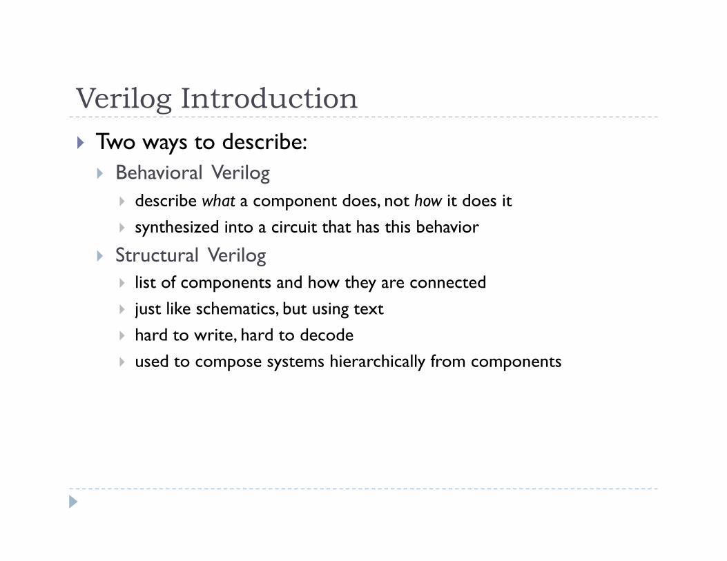
Verilog Introduction Two ways to describe:
Behavioral Verilog describe what a component does, not how it does it synthesized into a circuit that has this behavior
Structural Verilog list of components and how they are connected just like schematics, but using text hard to write, hard to decode used to compose systems hierarchically from components
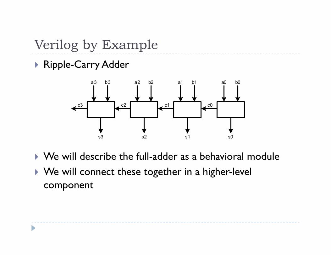
Verilog by Example Ripple-Carry Adder
We will describe the full-adder as a behavioral module We will connect these together in a higher-level
component
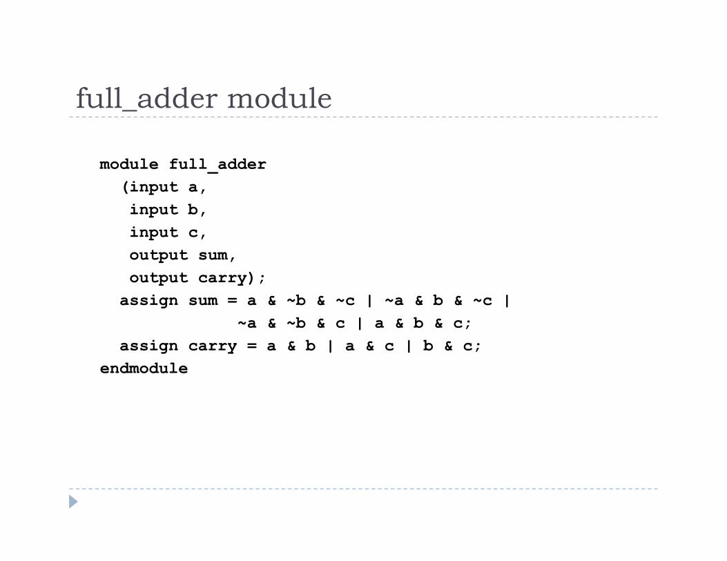
full_adder module
module full_adder (input a, input b, input c, output sum, output carry); assign sum = a & ~b & ~c | ~a & b & ~c | ~a & ~b & c | a & b & c; assign carry = a & b | a & c | b & c; endmodule
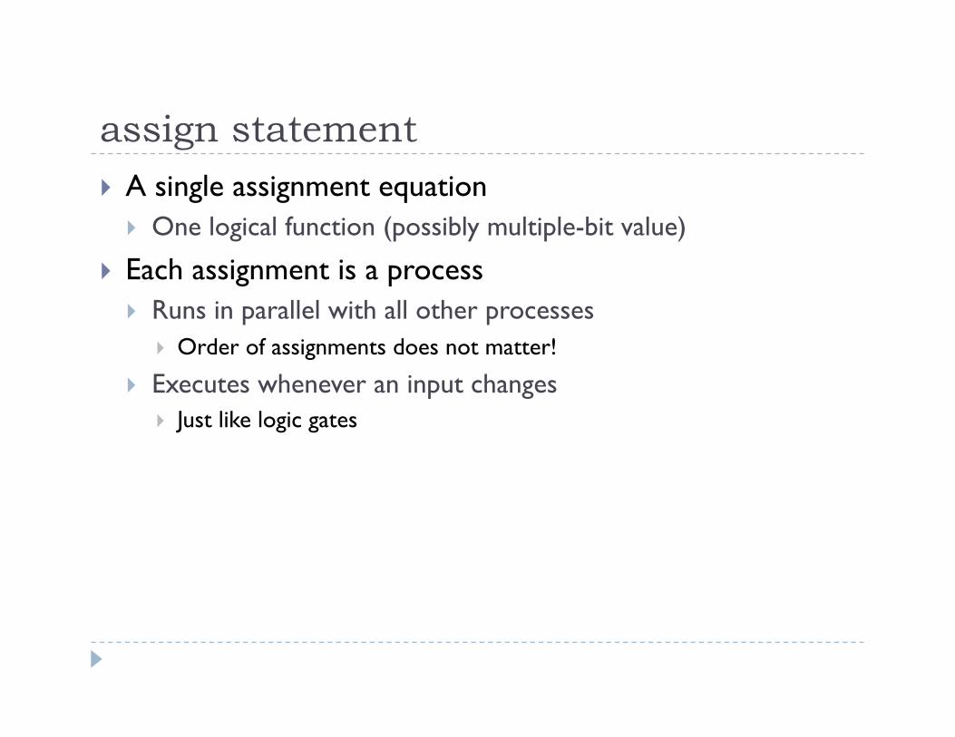
assign statement A single assignment equation
One logical function (possibly multiple-bit value)
Each assignment is a process Runs in parallel with all other processes
Order of assignments does not matter!
Executes whenever an input changes Just like logic gates
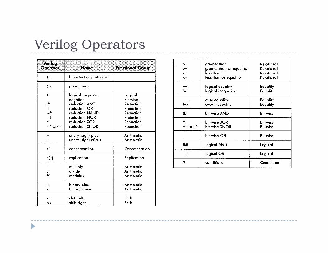
Verilog Operators
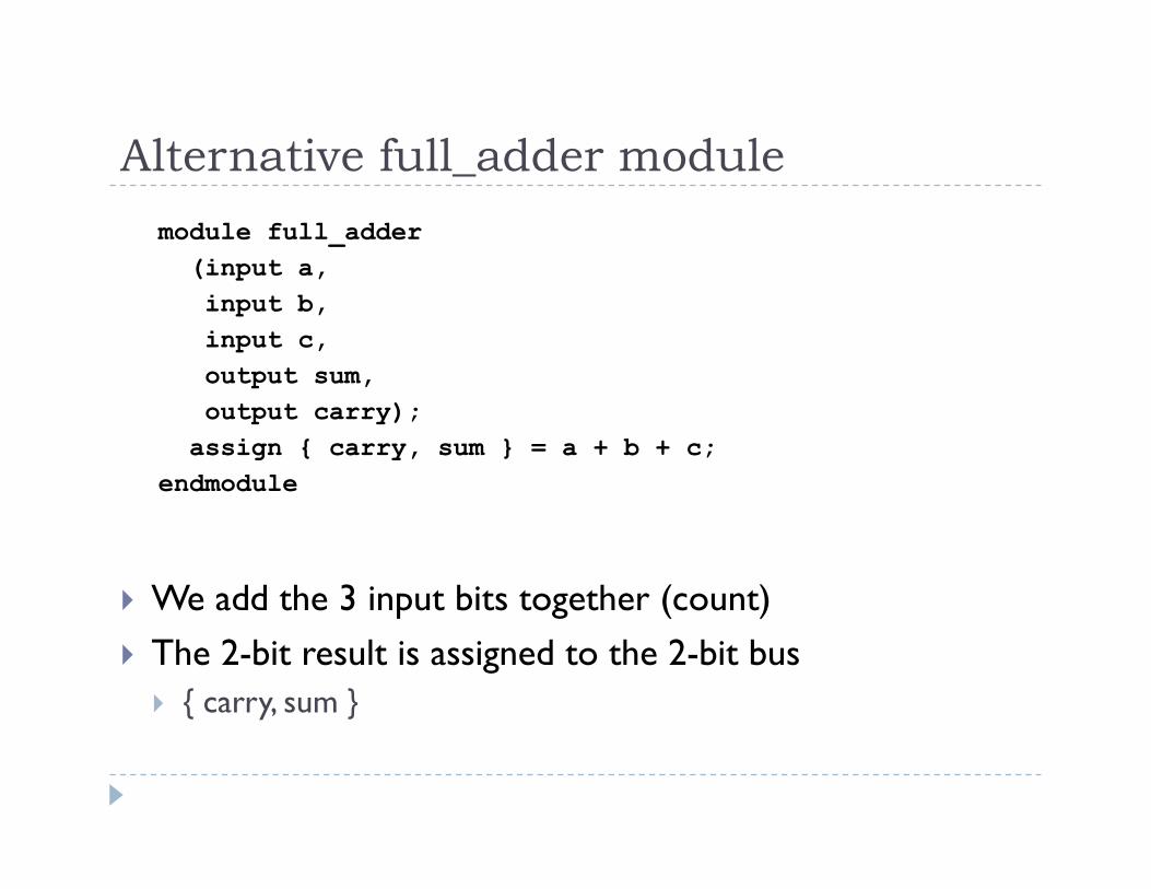
Alternative full_adder module
We add the 3 input bits together (count) The 2-bit result is assigned to the 2-bit bus
{ carry, sum }
module full_adder (input a, input b, input c, output sum, output carry); assign { carry, sum } = a + b + c; endmodule
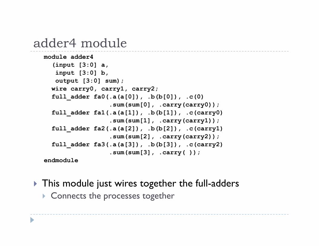
adder4 module
This module just wires together the full-adders Connects the processes together
module adder4 (input [3:0] a, input [3:0] b, output [3:0] sum); wire carry0, carry1, carry2; full_adder fa0(.a(a[0]), .b(b[0]), .c(0) .sum(sum[0], .carry(carry0)); full_adder fa1(.a(a[1]), .b(b[1]), .c(carry0) .sum(sum[1], .carry(carry1)); full_adder fa2(.a(a[2]), .b(b[2]), .c(carry1) .sum(sum[2], .carry(carry2)); full_adder fa3(.a(a[3]), .b(b[3]), .c(carry2) .sum(sum[3], .carry( )); endmodule
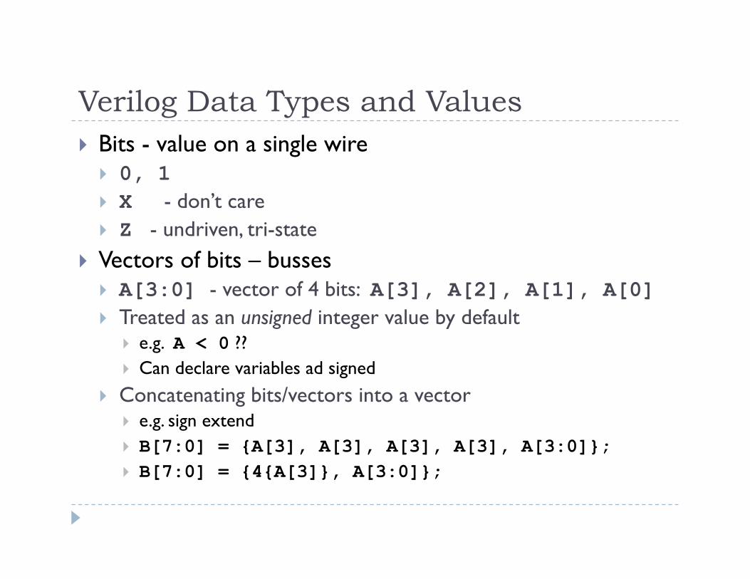
Verilog Data Types and Values Bits - value on a single wire
0, 1 X - don’t care Z - undriven, tri-state
Vectors of bits – busses A[3:0] - vector of 4 bits: A[3], A[2], A[1], A[0] Treated as an unsigned integer value by default
e.g. A < 0 ?? Can declare variables ad signed
Concatenating bits/vectors into a vector e.g. sign extend B[7:0] = {A[3], A[3], A[3], A[3], A[3:0]}; B[7:0] = {4{A[3]}, A[3:0]};
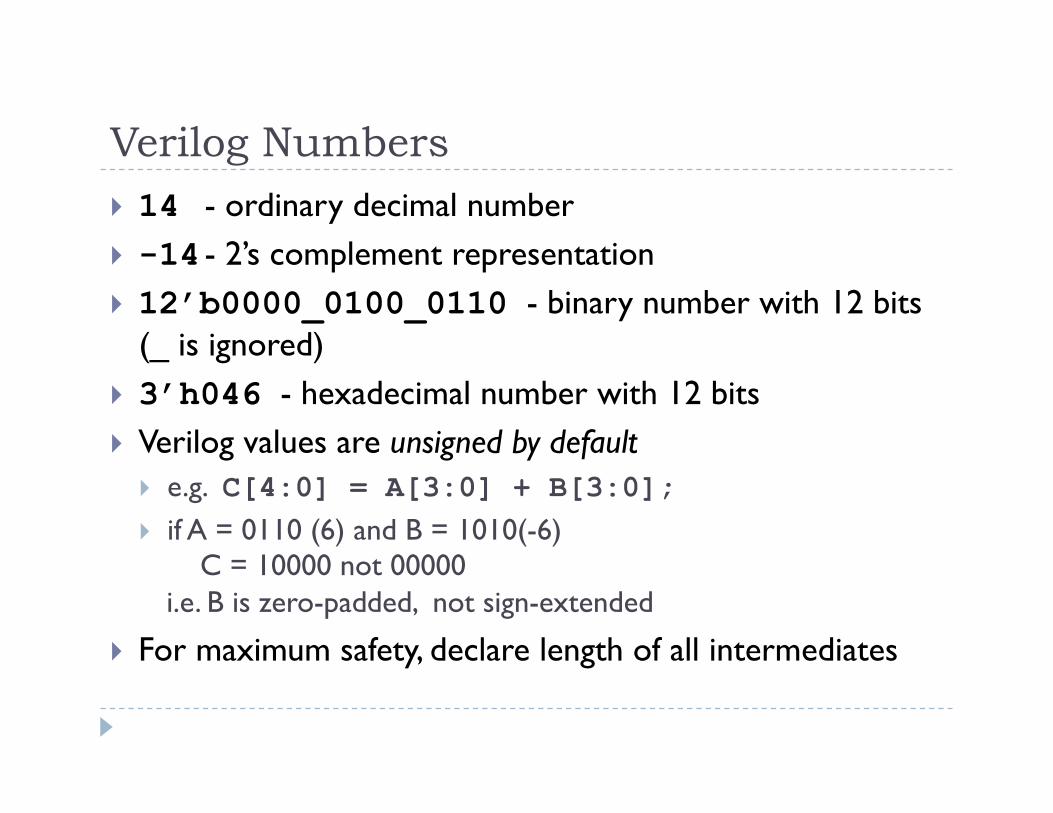
Verilog Numbers 14 - ordinary decimal number -14 - 2’s complement representation 12’b0000_0100_0110 - binary number with 12 bits
(_ is ignored) 3’h046 - hexadecimal number with 12 bits Verilog values are unsigned by default
e.g. C[4:0] = A[3:0] + B[3:0]; if A = 0110 (6) and B = 1010(-6)
C = 10000 not 00000 i.e. B is zero-padded, not sign-extended
For maximum safety, declare length of all intermediates

always block Contains a small program that is executed whenever an
input changes A parallel process, just like an assign statement The block can make multiple assignments The program is executed sequentially The program describes the function computed by the block Program is interpreted at compile time to generate a circuit Combinational – takes no time
Even though the program semantics are sequential
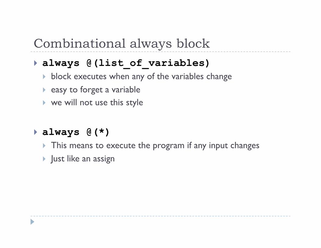
Combinational always block always @(list_of_variables)
block executes when any of the variables change easy to forget a variable we will not use this style
always @(*) This means to execute the program if any input changes Just like an assign
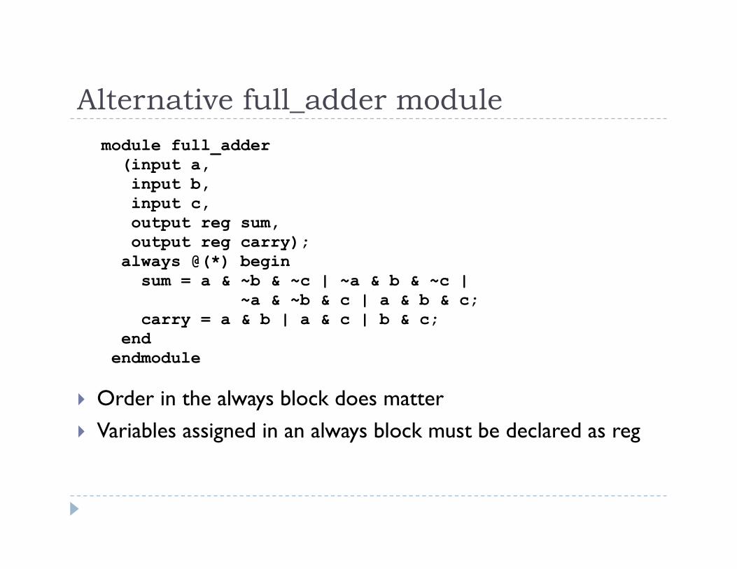
Alternative full_adder module
Order in the always block does matter Variables assigned in an always block must be declared as reg
module full_adder (input a, input b, input c, output reg sum, output reg carry); always @(*) begin sum = a & ~b & ~c | ~a & b & ~c | ~a & ~b & c | a & b & c; carry = a & b | a & c | b & c; end endmodule

Verilog Variables wire
variable used to connect components together inputs and outputs are wires by default
outputs be declared as regs
reg Any variable that is assigned in an always block
cannot be assigned by an assign statement
usually corresponds to a wire in the circuit is NOT a register in the circuit
Important: The names wire and reg do not mean anything!
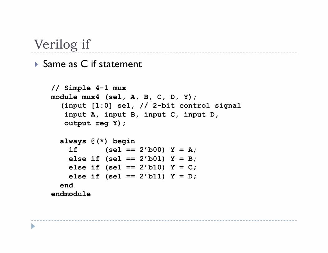
Verilog if Same as C if statement
// Simple 4-1 mux module mux4 (sel, A, B, C, D, Y); (input [1:0] sel, // 2-bit control signal input A, input B, input C, input D, output reg Y);
always @(*) begin if (sel == 2’b00) Y = A; else if (sel == 2’b01) Y = B; else if (sel == 2’b10) Y = C; else if (sel == 2’b11) Y = D; end endmodule
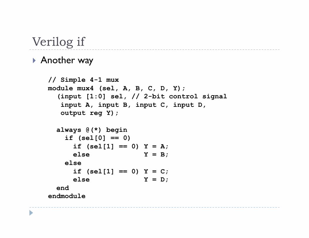
Verilog if Another way
// Simple 4-1 mux module mux4 (sel, A, B, C, D, Y); (input [1:0] sel, // 2-bit control signal input A, input B, input C, input D, output reg Y);
always @(*) begin if (sel[0] == 0) if (sel[1] == 0) Y = A; else Y = B; else if (sel[1] == 0) Y = C; else Y = D; end endmodule
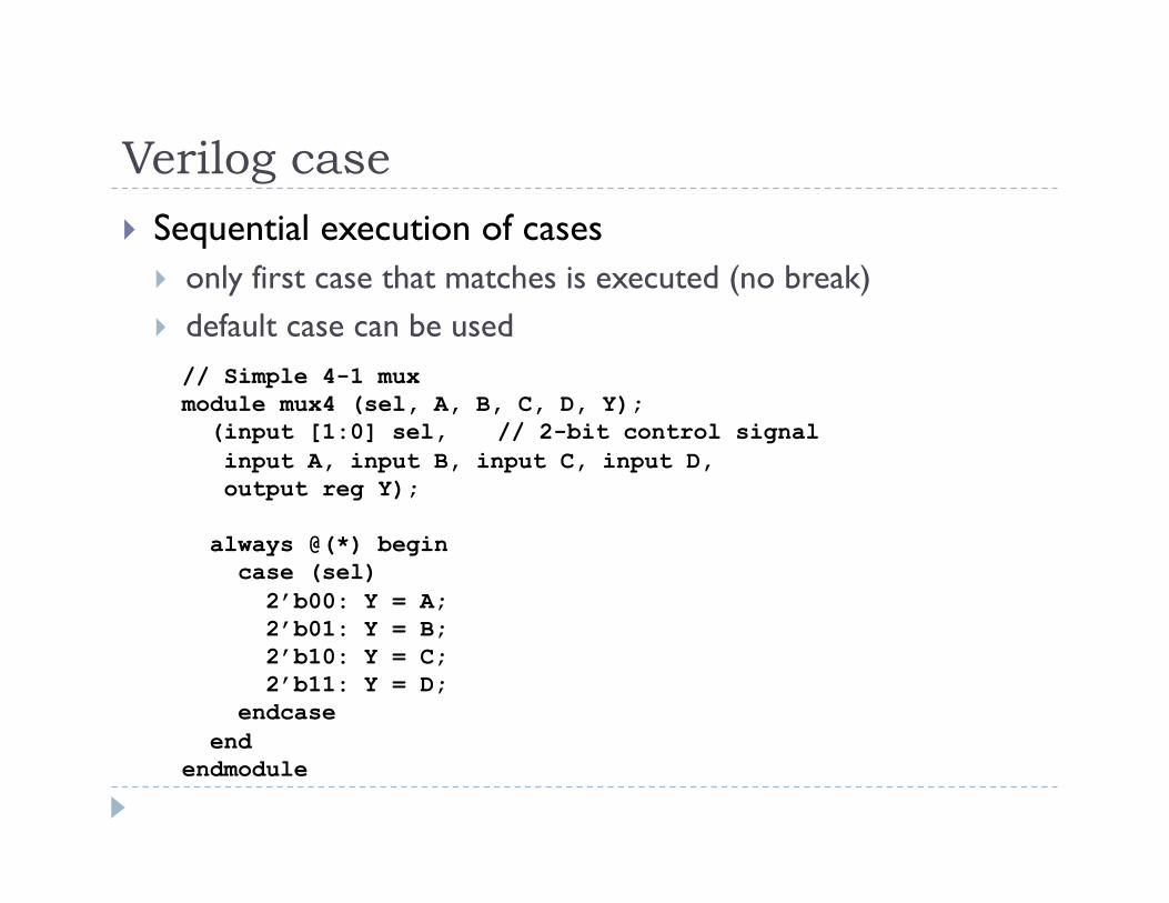
Verilog case Sequential execution of cases
only first case that matches is executed (no break) default case can be used // Simple 4-1 mux module mux4 (sel, A, B, C, D, Y); (input [1:0] sel, // 2-bit control signal input A, input B, input C, input D, output reg Y);
always @(*) begin case (sel) 2’b00: Y = A; 2’b01: Y = B; 2’b10: Y = C; 2’b11: Y = D; endcase end endmodule
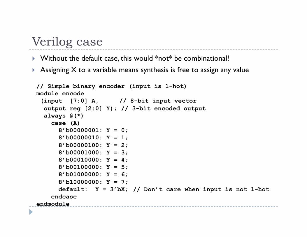
Verilog case Without the default case, this would *not* be combinational! Assigning X to a variable means synthesis is free to assign any value
// Simple binary encoder (input is 1-hot) module encode (input [7:0] A, // 8-bit input vector output reg [2:0] Y); // 3-bit encoded output always @(*) case (A) 8’b00000001: Y = 0; 8’b00000010: Y = 1; 8’b00000100: Y = 2; 8’b00001000: Y = 3; 8’b00010000: Y = 4; 8’b00100000: Y = 5; 8’b01000000: Y = 6; 8’b10000000: Y = 7; default: Y = 3’bX; // Don’t care when input is not 1-hot endcase endmodule
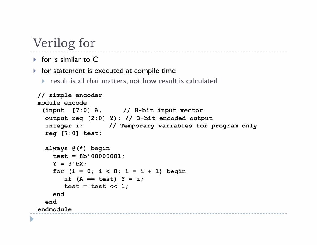
Verilog for for is similar to C for statement is executed at compile time
result is all that matters, not how result is calculated
// simple encoder module encode (input [7:0] A, // 8-bit input vector output reg [2:0] Y); // 3-bit encoded output integer i; // Temporary variables for program only reg [7:0] test;
always @(*) begin test = 8b’00000001; Y = 3’bX; for (i = 0; i < 8; i = i + 1) begin if (A == test) Y = i; test = test << 1; end end endmodule
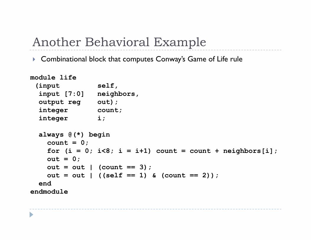
Another Behavioral Example Combinational block that computes Conway’s Game of Life rule
module life (input self, input [7:0] neighbors, output reg out); integer count; integer i;
always @(*) begin count = 0; for (i = 0; i<8; i = i+1) count = count + neighbors[i]; out = 0; out = out | (count == 3); out = out | ((self == 1) & (count == 2)); end endmodule
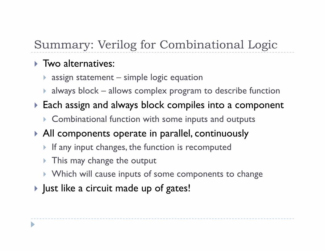
Summary: Verilog for Combinational Logic
Two alternatives: assign statement – simple logic equation always block – allows complex program to describe function
Each assign and always block compiles into a component Combinational function with some inputs and outputs
All components operate in parallel, continuously If any input changes, the function is recomputed This may change the output Which will cause inputs of some components to change
Just like a circuit made up of gates!
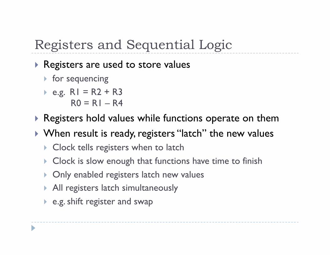
Registers and Sequential Logic Registers are used to store values
for sequencing e.g. R1 = R2 + R3
R0 = R1 – R4
Registers hold values while functions operate on them When result is ready, registers “latch” the new values
Clock tells registers when to latch Clock is slow enough that functions have time to finish Only enabled registers latch new values All registers latch simultaneously e.g. shift register and swap
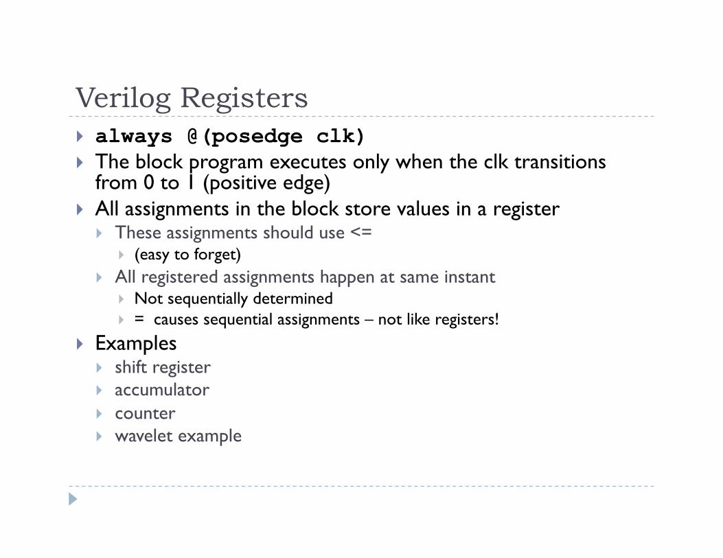
Verilog Registers always @(posedge clk) The block program executes only when the clk transitions
from 0 to 1 (positive edge) All assignments in the block store values in a register
These assignments should use <= (easy to forget)
All registered assignments happen at same instant Not sequentially determined = causes sequential assignments – not like registers!
Examples shift register accumulator counter wavelet example
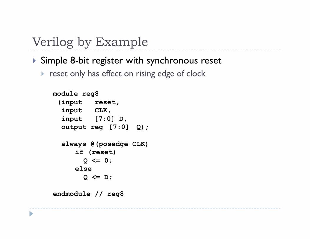
Verilog by Example Simple 8-bit register with synchronous reset
reset only has effect on rising edge of clock
module reg8 (input reset, input CLK, input [7:0] D, output reg [7:0] Q);
always @(posedge CLK) if (reset) Q <= 0; else Q <= D;
endmodule // reg8
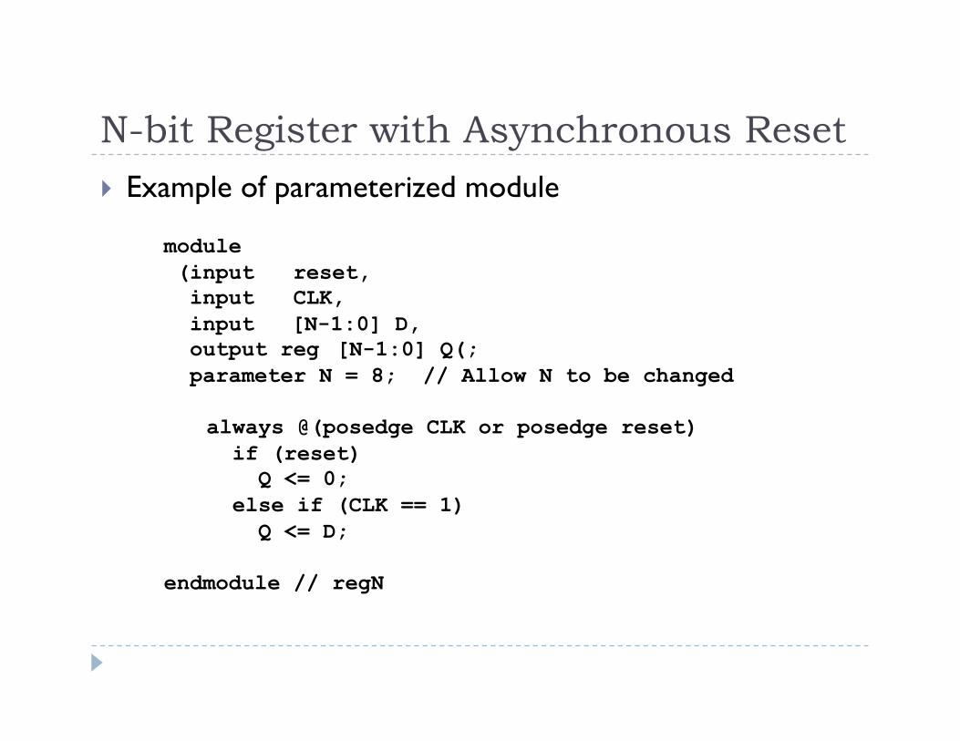
N-bit Register with Asynchronous Reset Example of parameterized module
module (input reset, input CLK, input [N-1:0] D, output reg [N-1:0] Q(; parameter N = 8; // Allow N to be changed
always @(posedge CLK or posedge reset) if (reset) Q <= 0; else if (CLK == 1) Q <= D;
endmodule // regN

Shift Register Example // 4 register shift register module shiftReg (input CLK, input reset, // initialize registers input shift, input [7:0] Din, // Data input for load output [7:0] Dout); reg [7:0] D0, D1, D2, D3; assign Dout = D0; always @(posedge CLK) begin if (reset) begin D0 <= 0; D1 <= 0; D2 <= 0; D3 <= 0; end else if (shift) begin D3 <= Din; D2 <= D3; D1 <= D2; D0 <= D1; end end
endmodule // shiftReg
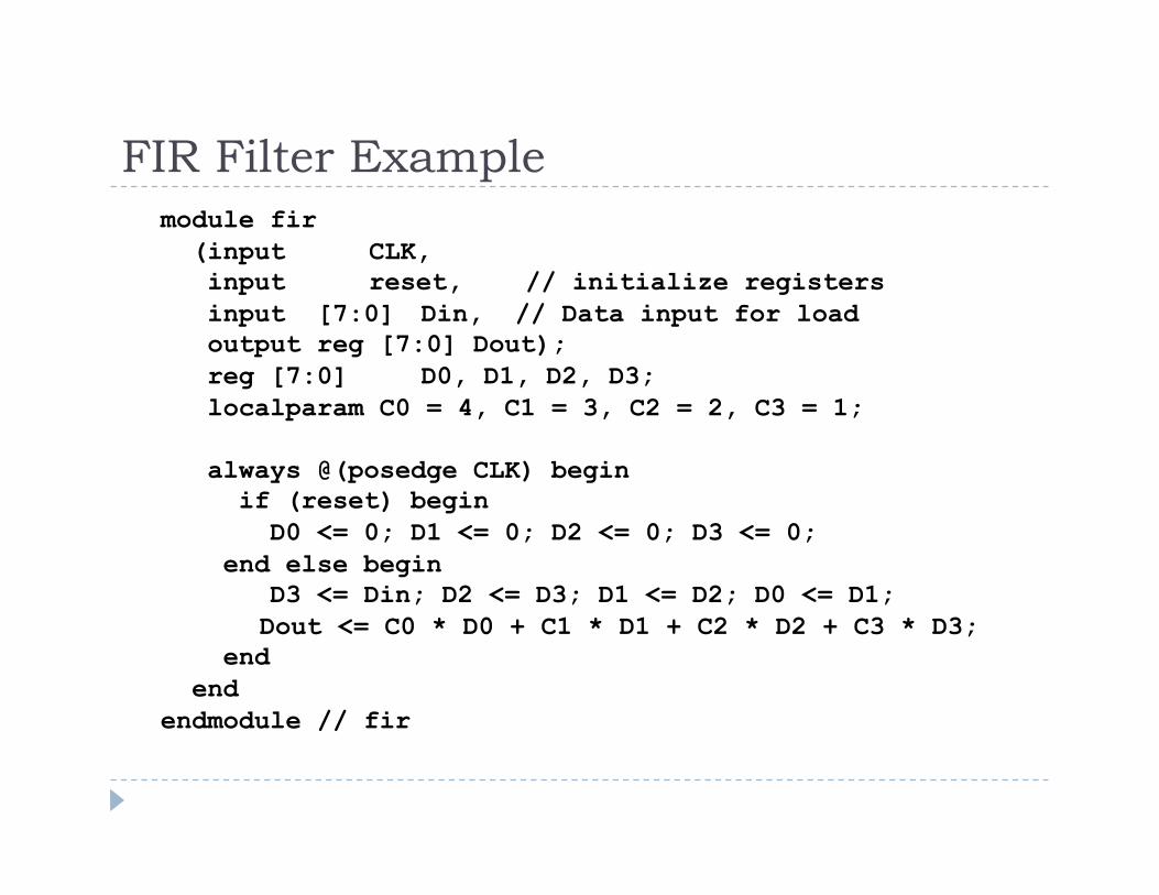
FIR Filter Example module fir (input CLK, input reset, // initialize registers input [7:0] Din, // Data input for load output reg [7:0] Dout); reg [7:0] D0, D1, D2, D3; localparam C0 = 4, C1 = 3, C2 = 2, C3 = 1;
always @(posedge CLK) begin if (reset) begin D0 <= 0; D1 <= 0; D2 <= 0; D3 <= 0; end else begin D3 <= Din; D2 <= D3; D1 <= D2; D0 <= D1;
Dout <= C0 * D0 + C1 * D1 + C2 * D2 + C3 * D3; end end endmodule // fir
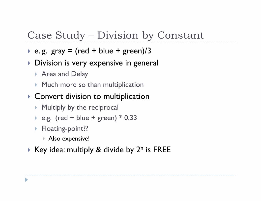
Case Study – Division by Constant e. g. gray = (red + blue + green)/3 Division is very expensive in general
Area and Delay Much more so than multiplication
Convert division to multiplication Multiply by the reciprocal e.g. (red + blue + green) * 0.33 Floating-point??
Also expensive!
Key idea: multiply & divide by 2n is FREE
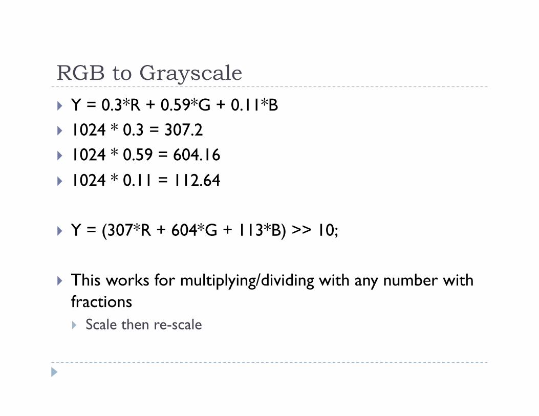
RGB to Grayscale Y = 0.3*R + 0.59*G + 0.11*B 1024 * 0.3 = 307.2 1024 * 0.59 = 604.16 1024 * 0.11 = 112.64
Y = (307*R + 604*G + 113*B) >> 10;
This works for multiplying/dividing with any number with fractions Scale then re-scale
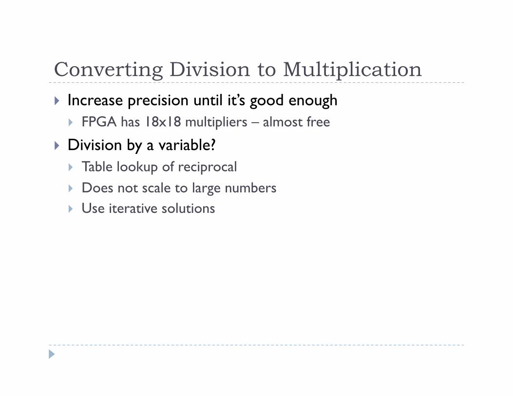
Converting Division to Multiplication Increase precision until it’s good enough
FPGA has 18x18 multipliers – almost free
Division by a variable? Table lookup of reciprocal Does not scale to large numbers Use iterative solutions