Lecture 6 2014 02 14 - Electronic System - Outcome2.1 (Analysis of Biasing of the FET)

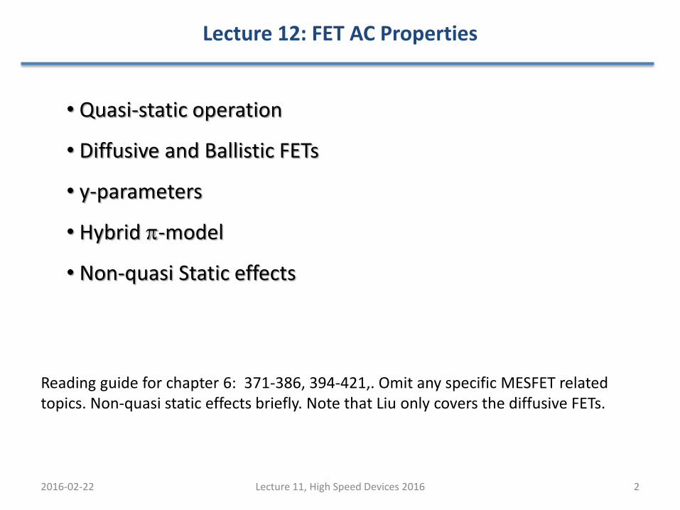
Lecture 12: FET AC Properties
2016-02-22 1Lecture 11, High Speed Devices 2016
Lecture 12: FET AC Properties
2016-02-22 2Lecture 11, High Speed Devices 2016
• Quasi-static operation
• Diffusive and Ballistic FETs
• y-parameters
• Hybrid p-model
• Non-quasi Static effects
Reading guide for chapter 6: 371-386, 394-421,. Omit any specific MESFET related topics. Non-quasi static effects briefly. Note that Liu only covers the diffusive FETs.
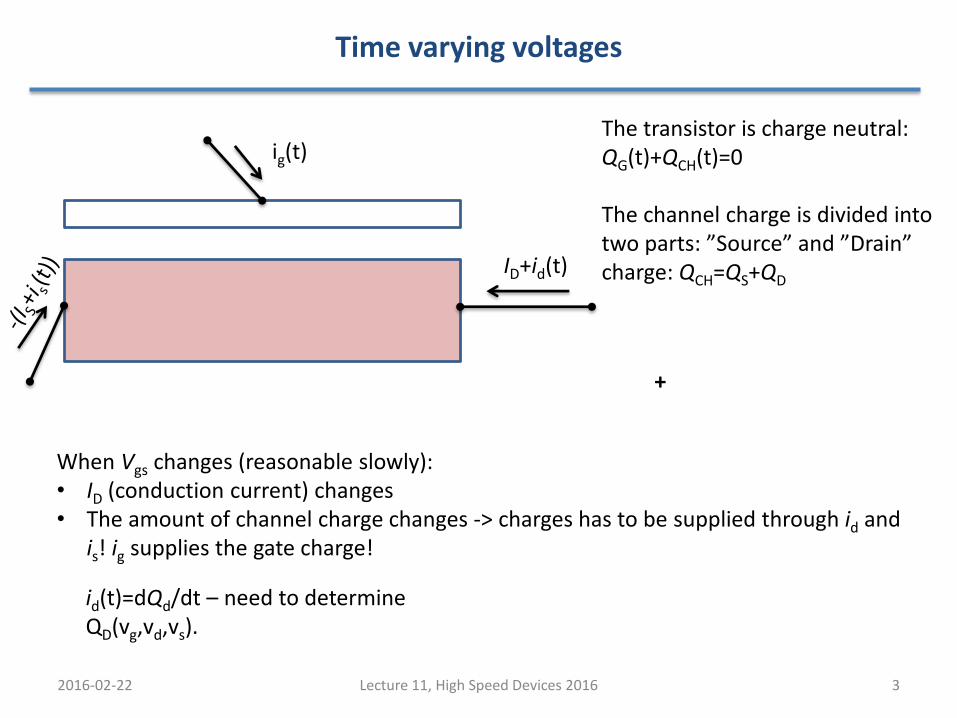
Time varying voltages
2016-02-22 3Lecture 11, High Speed Devices 2016
The transistor is charge neutral:QG(t)+QCH(t)=0
The channel charge is divided intotwo parts: ”Source” and ”Drain” charge: QCH=QS+QD
ig(t)
ID+id(t)
When Vgs changes (reasonable slowly):• ID (conduction current) changes• The amount of channel charge changes -> charges has to be supplied through id and
is! ig supplies the gate charge!
+
id(t)=dQd/dt – need to determineQD(vg,vd,vs).
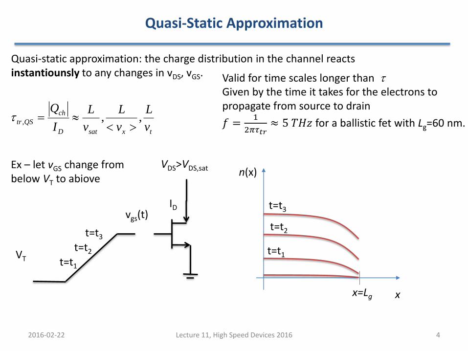
Quasi-Static Approximation
2016-02-22 4Lecture 11, High Speed Devices 2016
VT
vgs(t)ID
Quasi-static approximation: the charge distribution in the channel reactsinstantiounsly to any changes in vDS, vGS.
t=t1
t=t2
t=t3
txsatD
ch
QStrv
L
v
L
v
L
I
Q,,,
x
n(x)
x=Lg
Valid for time scales longer than Given by the time it takes for the electrons to propagate from source to drain
𝑓 =1
2𝜋𝜏𝑡𝑟≈ 5 𝑇𝐻𝑧 for a ballistic fet with Lg=60 nm.
VDS>VDS,sat
t=t1
t=t2
t=t3
Ex – let vGS change from below VT to abiove
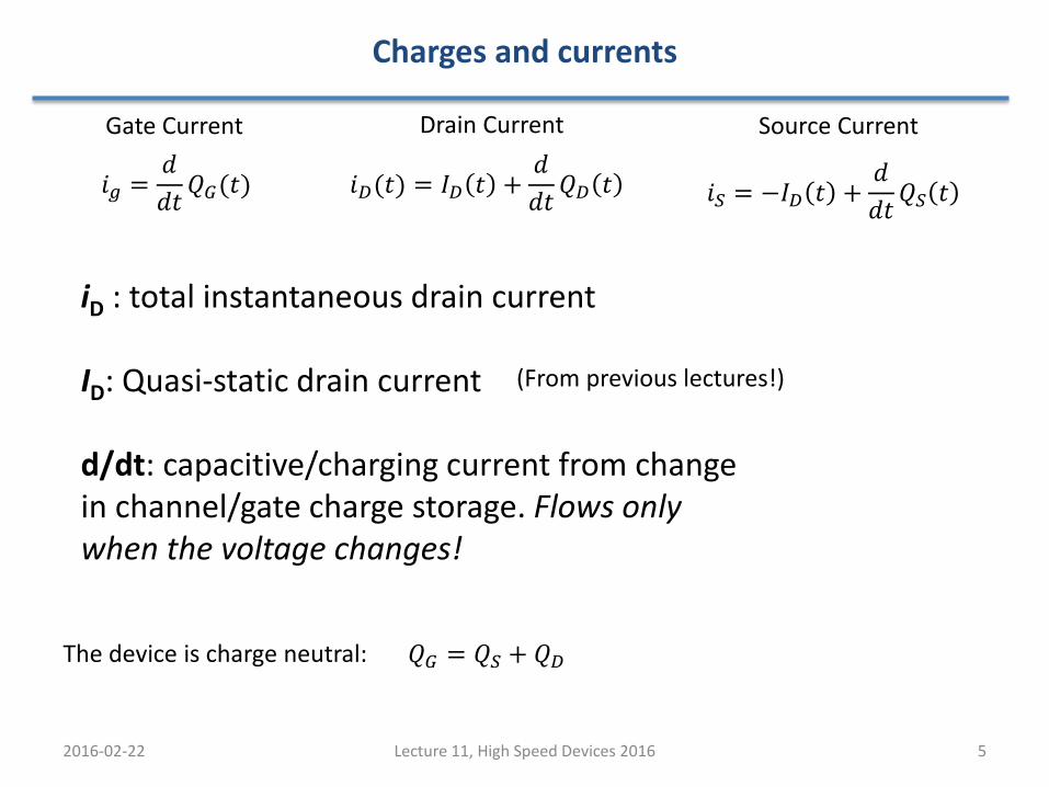
Charges and currents
2016-02-22 5Lecture 11, High Speed Devices 2016
𝑖𝑔 =𝑑
𝑑𝑡𝑄𝐺(𝑡) 𝑖𝐷(𝑡) = 𝐼𝐷 𝑡 +
𝑑
𝑑𝑡𝑄𝐷 𝑡 𝑖𝑆 = −𝐼𝐷 𝑡 +
𝑑
𝑑𝑡𝑄𝑆 𝑡
iD : total instantaneous drain current
ID: Quasi-static drain current
d/dt: capacitive/charging current from changein channel/gate charge storage. Flows onlywhen the voltage changes!
Gate Current Drain Current Source Current
𝑄𝐺 = 𝑄𝑆 + 𝑄𝐷The device is charge neutral:
(From previous lectures!)
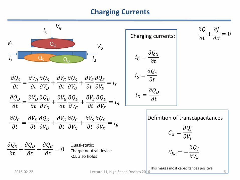
Charging Currents
2016-02-22 6Lecture 11, High Speed Devices 2016
𝜕𝑄
𝜕𝑡+𝜕𝐽
𝜕𝑥= 0
𝜕𝑄𝑆𝜕𝑡+𝜕𝑄𝐷𝜕𝑡+𝜕𝑄𝐺𝜕𝑡
= 0
𝜕𝑄𝑆𝜕𝑡=𝜕𝑉𝐷𝜕𝑡
𝜕𝑄𝑆𝜕𝑉𝐷
+𝜕𝑉𝐺𝜕𝑡
𝜕𝑄𝑆𝜕𝑉𝐺
+𝜕𝑉𝑆𝜕𝑡
𝜕𝑄𝑆𝜕𝑉𝑆
= 𝑖𝑠
𝜕𝑄𝐷𝜕𝑡
=𝜕𝑉𝐷𝜕𝑡
𝜕𝑄𝐷𝜕𝑉𝐷
+𝜕𝑉𝐺𝜕𝑡
𝜕𝑄𝐷𝜕𝑉𝐺
+𝜕𝑉𝑆𝜕𝑡
𝜕𝑄𝐷𝜕𝑉𝑆
= 𝑖𝑑
𝜕𝑄𝐺𝜕𝑡
=𝜕𝑉𝐷𝜕𝑡
𝜕𝑄𝐺𝜕𝑉𝐷
+𝜕𝑉𝐺𝜕𝑡
𝜕𝑄𝐺𝜕𝑉𝐺
+𝜕𝑉𝑆𝜕𝑡
𝜕𝑄𝐺𝜕𝑉𝑆
= 𝑖𝑔
VD
VG
Charging currents:
𝑖𝐺 =𝜕𝑄𝐺𝜕𝑡
𝑖𝑆 =𝜕𝑄𝑠𝜕𝑡
𝑖𝐷 =𝜕𝑄𝐷𝜕𝑡
VS
QS QD
QG
id
ig
is
𝐶𝑖𝑖 =𝜕𝑄𝑖𝜕𝑉𝑖
𝐶𝑗𝑘 = −𝜕𝑄𝑗
𝜕𝑉𝑘
Definition of transcapacitances
Quasi-static:Charge neutral deviceKCL also holds
This makes most capacitances positive
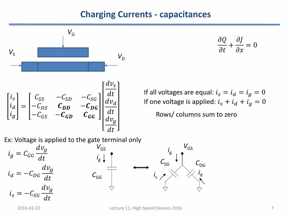
Charging Currents - capacitances
2016-02-22 7Lecture 11, High Speed Devices 2016
𝜕𝑄
𝜕𝑡+𝜕𝐽
𝜕𝑥= 0
VD
VG
VS
𝑖𝑠𝑖𝑑𝑖𝑔
=
𝐶𝑆𝑆 −𝐶𝑆𝐷 −𝐶𝑆𝐺−𝐶𝐷𝑆 𝑪𝑫𝑫 −𝑪𝑫𝑮−𝐶𝐺𝑆 −𝑪𝑮𝑫 𝑪𝑮𝑮
𝑑𝑣𝑠𝑑𝑡𝑑𝑣𝑑𝑑𝑡𝑑𝑣𝑔
𝑑𝑡
If all voltages are equal: 𝑖𝑠 = 𝑖𝑑 = 𝑖𝑔 = 0
If one voltage is applied: 𝑖𝑠 + 𝑖𝑑 + 𝑖𝑔 = 0
Rows/ columns sum to zero
𝑖𝑔 = 𝐶𝐺𝐺𝑑𝑣𝑔
𝑑𝑡
𝑖𝑑 = −𝐶𝐷𝐺𝑑𝑣𝑔
𝑑𝑡
𝑖𝑠 = −𝐶𝑆𝐺𝑑𝑣𝑔
𝑑𝑡
Ex: Voltage is applied to the gate terminal only
CGG
ig
VGSVGS
isid
CSG CDG
ig

Charging Current / total Current
2016-02-22 8Lecture 11, High Speed Devices 2016
𝑖𝑠𝑖𝑑𝑖𝑔
=
𝐶𝑆𝑆 −𝐶𝑆𝐷 −𝐶𝑆𝐺−𝐶𝐷𝑆 𝑪𝑫𝑫 −𝑪𝑫𝑮−𝐶𝐺𝑆 −𝑪𝑮𝑫 𝑪𝑮𝑮
𝑑𝑣𝑠𝑑𝑡𝑑𝑣𝑑𝑑𝑡𝑑𝑣𝑔
𝑑𝑡
𝑖𝑔𝑖𝑑=
𝐶𝐺𝐺 −𝐶𝐺𝐷−𝐶𝐷𝐺 𝐶𝐷𝐷
𝜕𝑣𝐺𝑆𝜕𝑡𝜕𝑣𝐷𝑆𝜕𝑡
𝑖𝐷 = 𝐼𝐷 𝑣𝐺𝑆, 𝑣𝐷𝑆 + 𝐶𝐷𝐷 𝑣𝐺𝑆, 𝑣𝐷𝑆𝜕𝑣𝐺𝑆𝜕𝑡
− 𝐶𝐷𝐺 𝑣𝐺𝑆, 𝑣𝐷𝑆𝜕𝑣𝐷𝑆𝜕𝑡
𝑖𝐺 = 𝐶𝐺𝐺 𝑣𝐺𝑆, 𝑣𝐷𝑆𝜕𝑣𝐺𝑆𝜕𝑡
− 𝐶𝐺𝐷 𝑣𝐺𝑆, 𝑣𝐷𝑆𝜕𝑣𝐷𝑆𝜕𝑡
Large Signal, Quasi-static FET model
We need to calculate– QG(VGS,VDS) and QD(VGS,VDS)
Common Source

Diffusive FET Gate Charge: QG
2016-02-22 9Lecture 11, High Speed Devices 2016
Negative channel charges divides onto drain and source chargesPositive charge on gate terminal to make device neutral
1
1
3
2,,11),0(,)(
2'
0 0
2'
Tgsox
L L
dgsCHCHoxG VvWLCvvvL
xtudxtxuWCtQ
Total Gate charge:
-
+++ ++ ++ +
++ ++
- -- - -- - -- ---
QG
QDQS
More positive gate bias – more positive charge on the gateCharge neutral device: More negative charge in the channel
𝑢𝑐ℎ 𝑥, 𝑡 = 𝑢𝑐ℎ 0, 𝑡 1 −𝑥
𝐿1 − 𝛼2 𝛼 =
1 −𝑣𝐷𝑆𝑉𝐷𝑆,𝑠𝑎𝑡
, 𝑉𝐷𝑆 < 𝑉𝐷𝑆,𝑠𝑎𝑡
0
𝑉𝐷𝑆,𝑠𝑎𝑡 = (𝑉𝐺𝑆 − 𝑉𝑇)
𝑛 𝑥, 𝑡 = 𝑊𝐶𝐺 𝑣𝐺𝑆 𝑡 − 𝑉𝑇 1 −𝑥
𝐿1 − 𝛼2

Ballistic FET Gate Charge: QG
2016-02-22 10Lecture 11, High Speed Devices 2016
EFS
LG
A real ballistic FET has a complicated band profileCrude approximation : constant potential until drain reservior
𝑛 𝑥 = 𝑛 0 = 𝐶𝐺′ (𝑣𝐺𝑆 − 𝑉𝑇)
𝑄𝐺 = 𝑊𝐿𝑔𝐶𝐺′ (𝑣𝐺𝑆 − 𝑉𝑇)
𝑄𝐺 =
0
𝐿𝐺
𝑛 𝑥 𝑑𝑥
Simplest possible assumption:
𝐶𝐺′ =
1
𝐶𝑜𝑥+2
𝐶𝑞+1
𝐶𝑐
−1
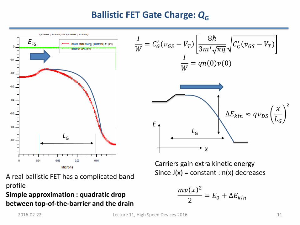
Ballistic FET Gate Charge: QG
2016-02-22 11Lecture 11, High Speed Devices 2016
EFS𝐼
𝑊= 𝐶𝐺
′ 𝑣𝐺𝑆 − 𝑉𝑇8ℏ
3𝑚∗ 𝜋𝑞𝐶𝐺′ 𝑣𝐺𝑆 − 𝑉𝑇
𝐼
𝑊= 𝑞𝑛 0 𝑣(0)
Δ𝐸𝑘𝑖𝑛 ≈ 𝑞𝑣𝐷𝑆𝑥
𝐿𝐺
2
LG
A real ballistic FET has a complicated band profileSimple approximation : quadratic drop between top-of-the-barrier and the drain
LG
Carriers gain extra kinetic energySince J(x) = constant : n(x) decreases
𝑚𝑣 𝑥 2
2= 𝐸0 + Δ𝐸𝑘𝑖𝑛
x
E
Ballistic FET Gate Charge: QG
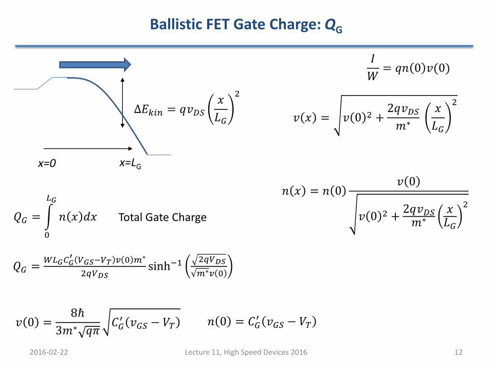
2016-02-22 12Lecture 11, High Speed Devices 2016
𝐼
𝑊= 𝑞𝑛 0 𝑣(0)
Δ𝐸𝑘𝑖𝑛 = 𝑞𝑣𝐷𝑆𝑥
𝐿𝐺
2
x=LG
𝑣 𝑥 = 𝑣 0 2 +2𝑞𝑣𝐷𝑆𝑚∗
𝑥
𝐿𝐺
2
𝑛 𝑥 = 𝑛 0𝑣 0
𝑣 0 2 +2𝑞𝑣𝐷𝑆𝑚∗
𝑥𝐿𝐺
2
x=0
𝑄𝐺 =𝑊𝐿𝐺𝐶𝐺
′ 𝑉𝐺𝑆−𝑉𝑇 𝑣 0 𝑚∗
2𝑞𝑉𝐷𝑆sinh−1
2𝑞𝑉𝐷𝑆
𝑚∗𝑣 0
𝑣 0 =8ℏ
3𝑚∗ 𝑞𝜋𝐶𝐺′ 𝑣𝐺𝑆 − 𝑉𝑇 𝑛 0 = 𝐶𝐺
′ 𝑣𝐺𝑆 − 𝑉𝑇
𝑄𝐺 =
0
𝐿𝐺
𝑛 𝑥 𝑑𝑥 Total Gate Charge
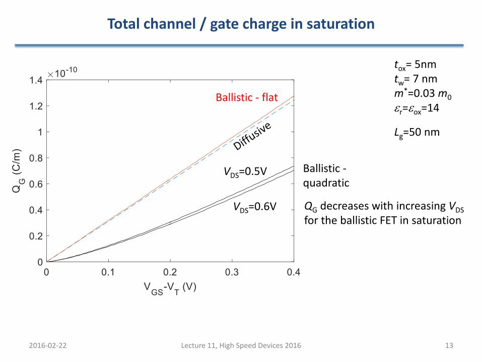
Total channel / gate charge in saturation
2016-02-22 13Lecture 11, High Speed Devices 2016
Lg=50 nm
Ballistic - flat
Ballistic -quadratic
VDS=0.5V
VDS=0.6V
tox= 5nmtw= 7 nmm*=0.03 m0
er=eox=14
QG decreases with increasing VDS
for the ballistic FET in saturation

QG for a ballistic FET in saturation
2016-02-22 14Lecture 11, High Speed Devices 2016
Ballistic -quadratic
VDS=0.5V
VDS=0.6V
QG decreased with increasing VDS since:
A) Less back injected drain chargeB) More back injected drain chargeC) Larger carrier velocity towards the drainD) Smaller carrier velocity towards the drainE) ???
0A B C D E
nano.participoll.com
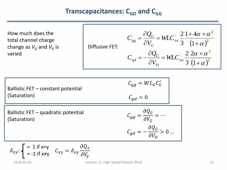
Transcapacitances: CGD and CGG
2016-02-22 15Lecture 11, High Speed Devices 2016
2
2'
1
41
3
2
ox
G
Ggg WLC
V
QC
2
2'
1
2
3
2
ox
D
Ggd WLC
V
QC
𝐶𝑥𝑦 = 𝛿𝑥𝑦𝜕𝑄𝑥𝜕𝑉𝑦
𝛿𝑥𝑦:= 1 if x=y= -1 if x≠y
Diffusive FET:
𝐶𝑔𝑔 = 𝑊𝐿𝐺𝐶𝐺′
How much does the total channel charge change as VG and VD is varied
𝐶𝑔𝑑 = 0
Ballistic FET – constant potential(Saturation)
Ballistic FET – quadratic potential(Saturation)
𝐶𝑔𝑔 =𝜕𝑄𝐺𝜕𝑉𝐺
= ⋯
𝐶𝑔𝑑 = −𝜕𝑄𝐺𝜕𝑉𝐷
> 0…
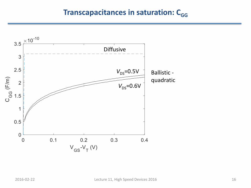
Transcapacitances in saturation: CGG
2016-02-22 16Lecture 11, High Speed Devices 2016
Diffusive
Ballistic -quadratic
VDS=0.5V
VDS=0.6V
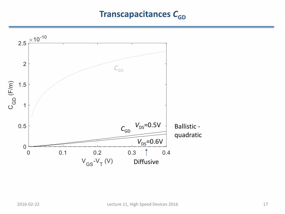
Transcapacitances CGD
2016-02-22 17Lecture 11, High Speed Devices 2016
CGG
CGDBallistic -quadratic
VDS=0.5V
VDS=0.6V
Diffusive

Drain Charges – Ballistic FET
2016-02-22 18Lecture 11, High Speed Devices 2016
Negative channel charges divides onto drain and source charges
-
+++ ++ ++ +
++ ++
- -- - -- - -- ---
QG
QDQS𝑄𝐺 + 𝑄𝑆 + 𝑄𝐷 = 0
QD: When QG changes – how much of that charge is ‘supplied’ from the drain?
QS – charge directly supplied from the source
QD – charge directly supplied from the drain
𝑛→ 𝑥 =𝐽→
𝑣+2(0) +
2𝑞𝑣𝐷𝑆𝑚∗
𝑥𝐿𝐺
2
𝑛← 𝑥 ≈𝐽←
𝑣−2 0 +
2𝑞𝑣𝐷𝑆𝑚∗
𝑥𝐿𝐺
2
≈ 0
𝑄𝑆 ∶ 𝐽→ 𝑄𝐷 ∶ 𝐽
←
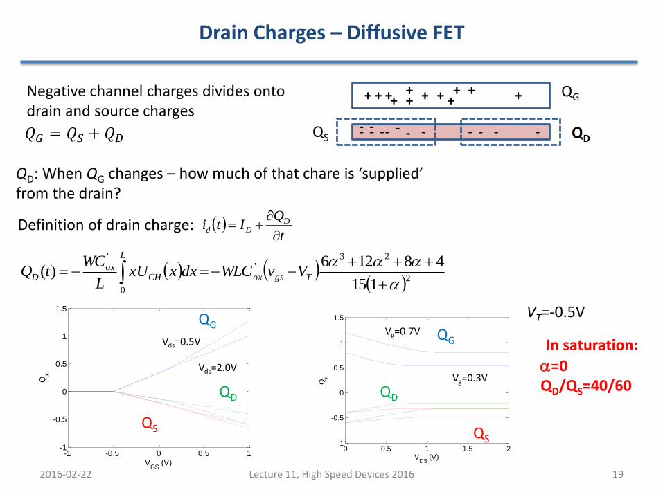
Drain Charges – Diffusive FET
2016-02-22 19Lecture 11, High Speed Devices 2016
Negative channel charges divides onto drain and source charges
-
+++ ++ ++ +
++ ++
- -- - -- - -- ---
QG
QDQS
2
23'
0
'
115
48126)(
Tgsox
L
CHox
D VvWLCdxxxUL
WCtQ
t
QIti D
Dd
Definition of drain charge:
=0QD/QS=40/60
0 0.5 1 1.5 2-1
-0.5
0
0.5
1
1.5
VDS
(V)
Qx
QG
QS
QD
VT=-0.5VVg=0.7V
Vg=0.3V
-1 -0.5 0 0.5 1-1
-0.5
0
0.5
1
1.5
VGS
(V)
Qx
QG
QD
QS
Vds=0.5V
Vds=2.0V
In saturation:
𝑄𝐺 = 𝑄𝑆 + 𝑄𝐷
QD: When QG changes – how much of that chare is ‘supplied’ from the drain?

Transcapacitances – Diffusive FET
2016-02-22 20Lecture 11, High Speed Devices 2016
2
2'
1
41
3
2
ox
G
Ggg WLC
V
QC
2
2'
1
2
3
2
ox
D
Ggd WLC
V
QC
3
32'
1
311142
15
2
ox
G
Ddg WLC
V
QC
3
32'
1
398
15
2
ox
D
Ddd WLC
V
QC
Note that Cdg ≠ Cgd
𝐶𝑥𝑦 = 𝛿𝑥𝑦𝜕𝑄𝑥𝜕𝑉𝑦
𝛿𝑥𝑦:= 1 if x=y= -1 if x≠y

Transcapacitances – Ballistic FET in saturation
2016-02-22 21Lecture 11, High Speed Devices 2016
𝑄𝐺 =𝑊𝐿𝐺𝐶𝐺
′ 𝑉𝐺𝑆−𝑉𝑇 𝑣 0 𝑚∗
2𝑞𝑉𝐷𝑆sinh−1
2𝑞𝑉𝐷𝑆
𝑚∗𝑣 0
𝑄𝑆 + 𝑄𝐺 = 0 𝑄𝐷 ≈ 0
𝐶𝐺𝐺 =𝜕𝑄𝐺𝜕𝑉𝐺
= 𝑊𝐿𝐺𝐶𝐺′ …
𝐶𝐺𝐷 = −𝜕𝑄𝐺𝜕𝑉𝐷
= 𝑊𝐿𝐺𝐶𝐺′ …
𝐶𝐷𝐺 = −𝜕𝑄𝐷𝜕𝑉𝐺
≈ 0
CGG
CGD
𝐶𝐷𝐷 =𝜕𝑄𝐷𝜕𝑉𝐷
≈ 0
Short channel effects can lead to negative CGD!
CDD,CGD

2 minutes excercise
2016-02-22 22Lecture 11, High Speed Devices 2016
2
2'
1
2
3
2
ox
D
Ggd WLC
V
QC
3
32'
1
311142
15
2
ox
G
Ddg WLC
V
QC
What is the physical reason that in saturation Cgd=0 and Cdg > 0 for an ideal, diffusive FET?
V
I
=0
A) The drain voltage does not influence the total channel charge after pinch-off
B) The gate voltage does not influence the total channel charge after pinch-off
C) QS+QD+QG=0 does not hold in saturation.D) This is due to approximations. Cij must
always be Cji.E) ???
0A B C D E
nano.participoll.com
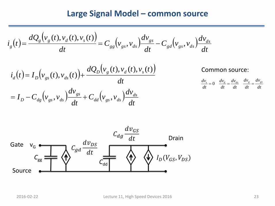
Large Signal Model – common source
2016-02-22 23Lecture 11, High Speed Devices 2016
Common source:
dt
dvvvC
dt
dvvvC
dt
tvtvtvdQti ds
dsgsgd
gs
dsgsgg
sdgg
g ,,)(),(),(
dt
dvvvC
dt
dvvvCI
dt
tvtvtvdQtvtvIti
dsdsgsdd
gs
dsgsdgD
sdgD
dsgsDd
,,
)(),(),()(),(
dt
dv
dt
dv
dt
dv
dt
dv
dt
dv gsgdsds 0
vG
Cgg
𝐶𝑔𝑑𝑑𝑣𝐷𝑆𝑑𝑡
Cdd
𝐶𝑑𝑔𝑑𝑣𝐺𝑆𝑑𝑡
𝐼𝐷(𝑉𝐺𝑆, 𝑉𝐷𝑆)
Gate
Source
Drain
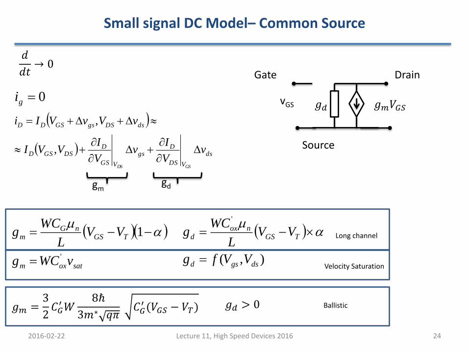
Small signal DC Model– Common Source
2016-02-22 24Lecture 11, High Speed Devices 2016
0gi
ds
VDS
Dgs
VGS
DDSGSD
dsDSgsGSDD
vV
Iv
V
IVVI
vVvVIi
GSDS
,
,
gmgd
satoxm
TGSnG
m
vWCg
VVL
WCg
'
1
),(
'
dsgsd
TGSnox
d
VVfg
VVL
WCg
Long channel
Velocity Saturation
vGS 𝑔𝑚𝑉𝐺𝑆
Gate
Source
Drain
𝑔𝑑
𝑑
𝑑𝑡→ 0
𝑔𝑚 =3
2𝐶𝐺′𝑊
8ℏ
3𝑚∗ 𝑞𝜋𝐶𝐺′ (𝑉𝐺𝑆 − 𝑉𝑇) 𝑔𝑑 > 0 Ballistic
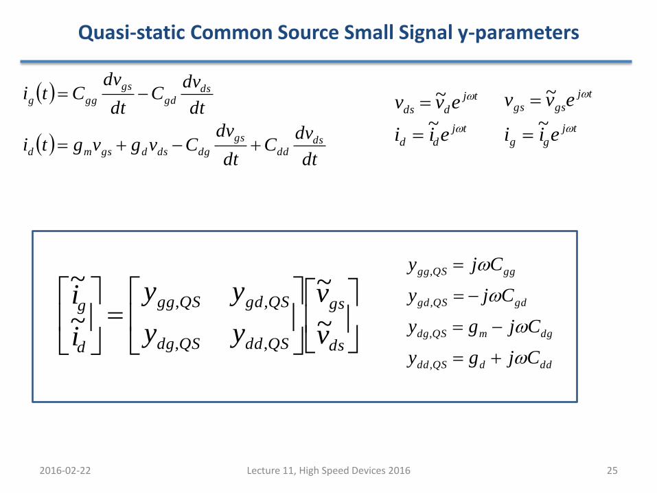
Quasi-static Common Source Small Signal y-parameters
2016-02-22 25Lecture 11, High Speed Devices 2016
dt
dvC
dt
dvCti ds
gd
gs
ggg
dt
dvC
dt
dvCvgvgti ds
dd
gs
dgdsdgsmd tj
dd
tj
dds
eii
evv
~
~
tj
gg
tj
gsgs
eii
evv
~
~
ds
gs
QSddQSdg
QSgdQSgg
d
g
v
v
yy
yy
i
i~
~
~
~
,,
,,
dddQSdd
dgmQSdg
gdQSgd
ggQSgg
Cjgy
Cjgy
Cjy
Cjy
,
,
,
,
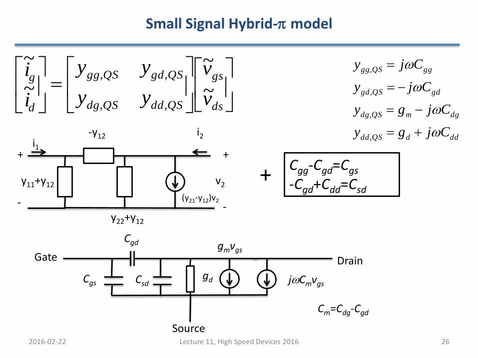
Small Signal Hybrid-p model
2016-02-22 26Lecture 11, High Speed Devices 2016
Cgd
Cgs Csdgd
Gate
jCmvgs
gmvgs
Drain
Source
Cm=Cdg-Cgd
ds
gs
QSddQSdg
QSgdQSgg
d
g
v
v
yy
yy
i
i~
~
~
~
,,
,,
dddQSdd
dgmQSdg
gdQSgd
ggQSgg
Cjgy
Cjgy
Cjy
Cjy
,
,
,
,
+
-
i1
y11+y12
(y21-y12)v2
-y12
y22+y12
v2
+
-
i2
Cgg-Cgd=Cgs
-Cgd+Cdd=Csd+

Small Signal Hybrid-p model
2016-02-22 27Lecture 11, High Speed Devices 2016
Cgd
Cgs Csdgd
Gate
jCmvgs
gmvgs
Drain
Source
Cm=Cdg-Cgd
General FET Model
Cgd
Cgs Csdgd
Gate
𝑔𝑚 − 𝑗𝜔𝐶𝑔𝑑 𝑣𝑔𝑠
Ballistic FET in saturation
Cgsgd
Gate
𝑔𝑚 + 𝑗𝜔𝐶𝑑𝑔 𝑣𝑔𝑠
Diffusive FET in saturation

Non-Quasi-Static
2016-02-22 28Lecture 11, High Speed Devices 2016
VT
vgs(t)
ID
For very short timescales:
Charges has to be supplied from the source – transient involves a charge-front –more complex math!
=0
)(,,
2
,
TGSnxsatD
ch
QStrVV
L
v
L
v
L
I
Q
txut
txux
ux
chchchn ,,
x
n(x)
x=Lg
𝑡 = ∞ 𝑠
t=t0 t0
t1
t2
t3
t4
t1 t2 t3 t4
Diffusive Transistor: Continuity and drift equation
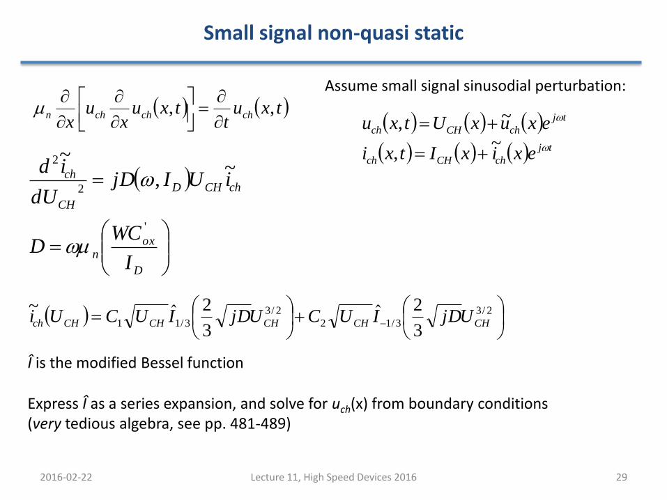
Small signal non-quasi static
2016-02-22 29Lecture 11, High Speed Devices 2016
txut
txux
ux
chchchn ,,
tj
chCHch
tj
chCHch
exixItxi
exuxUtxu
~,
~,
Assume small signal sinusodial perturbation:
D
oxn
chCHD
CH
ch
I
WCD
iUIjDdU
id
'
2
2~
,
~
2/3
3/12
2/3
3/113
2ˆ3
2ˆ~CHCHCHCHCHch UjDIUCUjDIUCUi
Î is the modified Bessel function
Express Î as a series expansion, and solve for uch(x) from boundary conditions(very tedious algebra, see pp. 481-489)
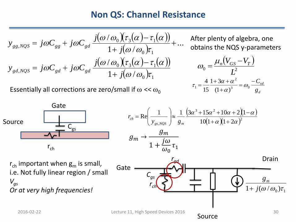
Non QS: Channel Resistance
2016-02-22 30Lecture 11, High Speed Devices 2016
10
130,
10
130,
/1
/
.../1
/
j
jCjCjy
j
jCjCjy
gdgdNQSgd
gdggNQSgg
After plenty of algebra, one obtains the NQS y-parameters
20
L
VV TGSn
Essentially all corrections are zero/small if << 0
Cgs
rch
Gate
Source
2
23
, 21110
121015311Re
mNQSgs
chgy
r
rch important when gm is small, i.e. Not fully linear region / small Vgs
Or at very high frequencies!
Cgs
GateDrain
Source
rch
rgd
d
sd
g
C
03
2
1)1(
31
15
4
10 )/(1 j
gm
𝑔𝑚 →𝑔𝑚
1 +𝑗𝜔𝜔0𝜏1
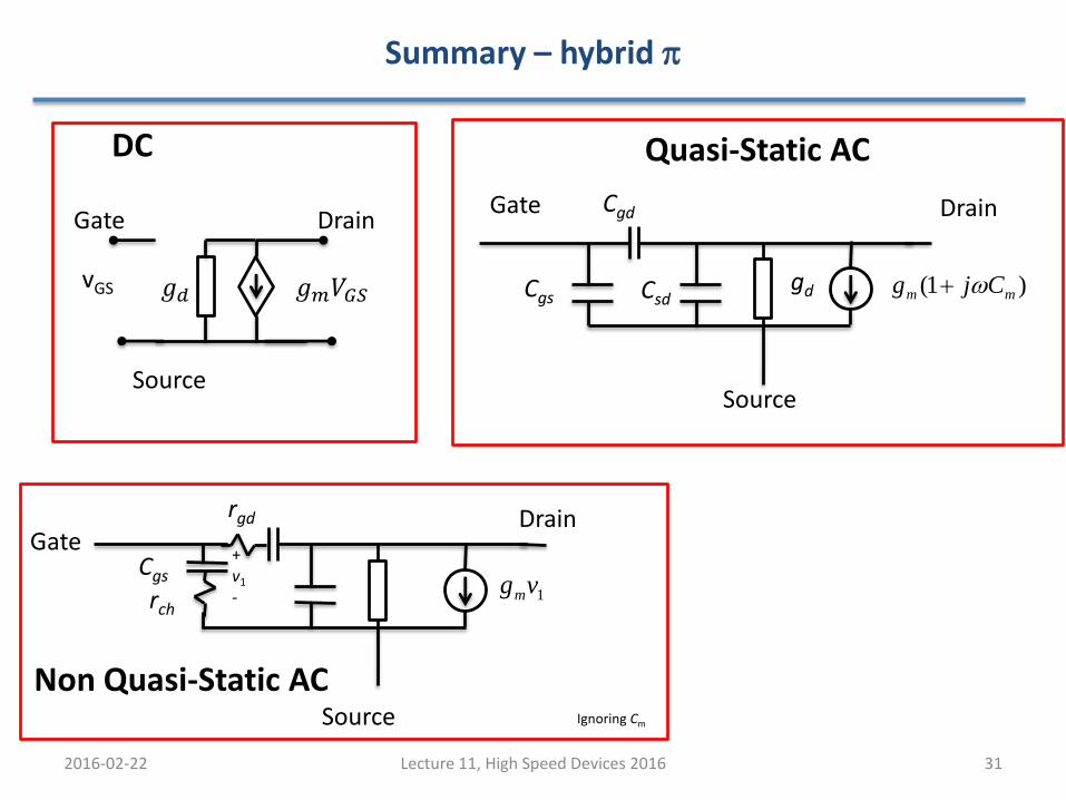
Summary – hybrid p
2016-02-22 31Lecture 11, High Speed Devices 2016
Cgs
GateDrain
Source
rch
rgd
1vgm
Cgd
Cgs Csdgd
Gate Drain
Source
)1( mm Cjg
Quasi-Static AC DC
Non Quasi-Static AC
vGS 𝑔𝑚𝑉𝐺𝑆
Gate
Source
Drain
𝑔𝑑
+v1
-
Ignoring Cm