
LECTURE 05 - PN JUNCTIONS AND CMOS …LECTURE 05 - PN JUNCTIONS AND CMOS TRANSISTORS LECTURE...
28
Lecture 05 – PN Junction and CMOS Transistors (8/5/14) Page 05-1 CMOS Analog Circuit Design © P.E. Allen - 2016 LECTURE 05 - PN JUNCTIONS AND CMOS TRANSISTORS LECTURE ORGANIZATION Outline • pn junctions • MOS transistors • Layout of MOS transistors • Parasitic bipolar transistors in CMOS technology • High voltage CMOS transistors • Summary CMOS Analog Circuit Design, 3 rd Edition Reference Pages 33-46 and 644-652
Transcript of LECTURE 05 - PN JUNCTIONS AND CMOS …LECTURE 05 - PN JUNCTIONS AND CMOS TRANSISTORS LECTURE...
Lecture 05 – PN Junction and CMOS Transistors (8/5/14) Page 05-1
CMOS Analog Circuit Design © P.E. Allen - 2016
LECTURE 05 - PN JUNCTIONS AND CMOS TRANSISTORS
LECTURE ORGANIZATION
Outline
• pn junctions
• MOS transistors
• Layout of MOS transistors
• Parasitic bipolar transistors in CMOS technology
• High voltage CMOS transistors
• Summary
CMOS Analog Circuit Design, 3rd Edition Reference
Pages 33-46 and 644-652
Lecture 05 – PN Junction and CMOS Transistors (8/5/14) Page 05-2
CMOS Analog Circuit Design © P.E. Allen - 2016
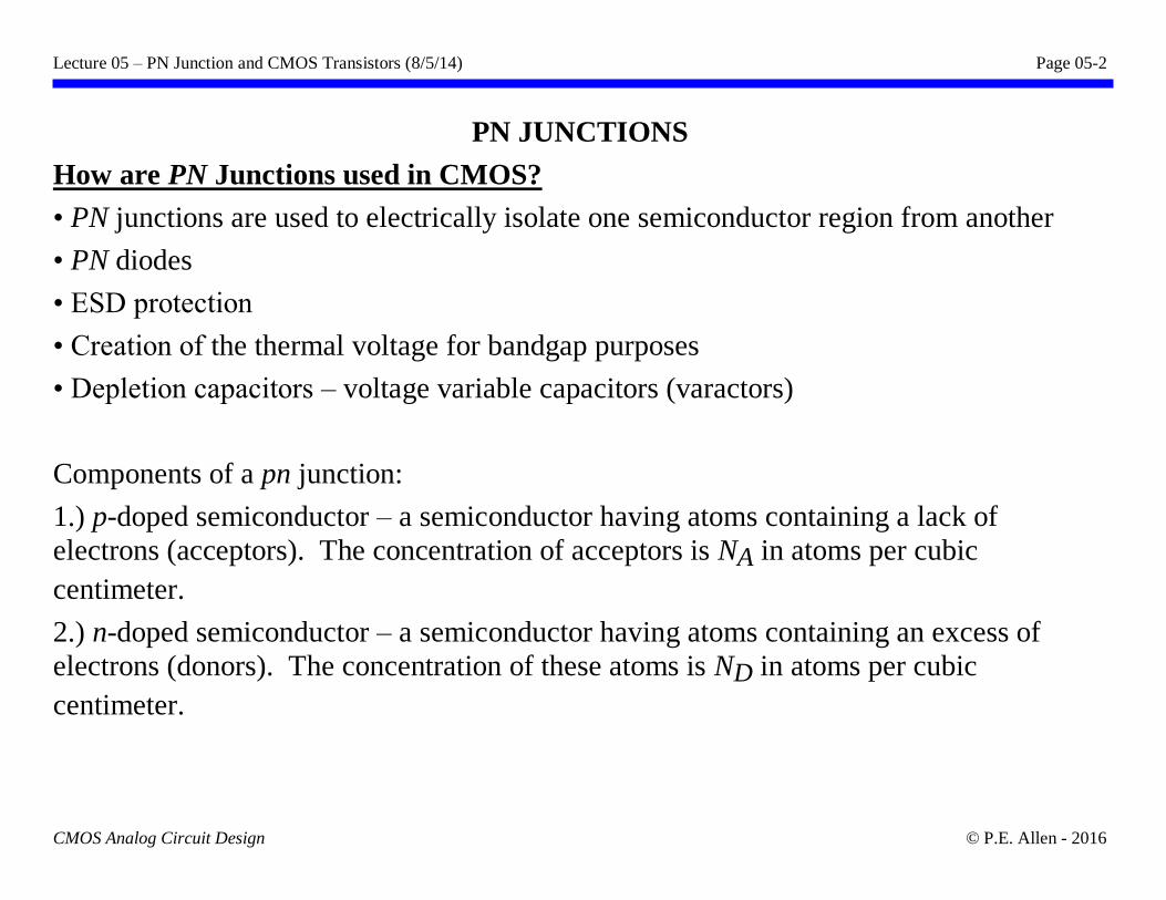
PN JUNCTIONS
How are PN Junctions used in CMOS?
• PN junctions are used to electrically isolate one semiconductor region from another
• PN diodes
• ESD protection
• Creation of the thermal voltage for bandgap purposes
• Depletion capacitors – voltage variable capacitors (varactors)
Components of a pn junction:
1.) p-doped semiconductor – a semiconductor having atoms containing a lack of
electrons (acceptors). The concentration of acceptors is NA in atoms per cubic
centimeter.
2.) n-doped semiconductor – a semiconductor having atoms containing an excess of
electrons (donors). The concentration of these atoms is ND in atoms per cubic
centimeter.
Lecture 05 – PN Junction and CMOS Transistors (8/5/14) Page 05-3
CMOS Analog Circuit Design © P.E. Allen - 2016
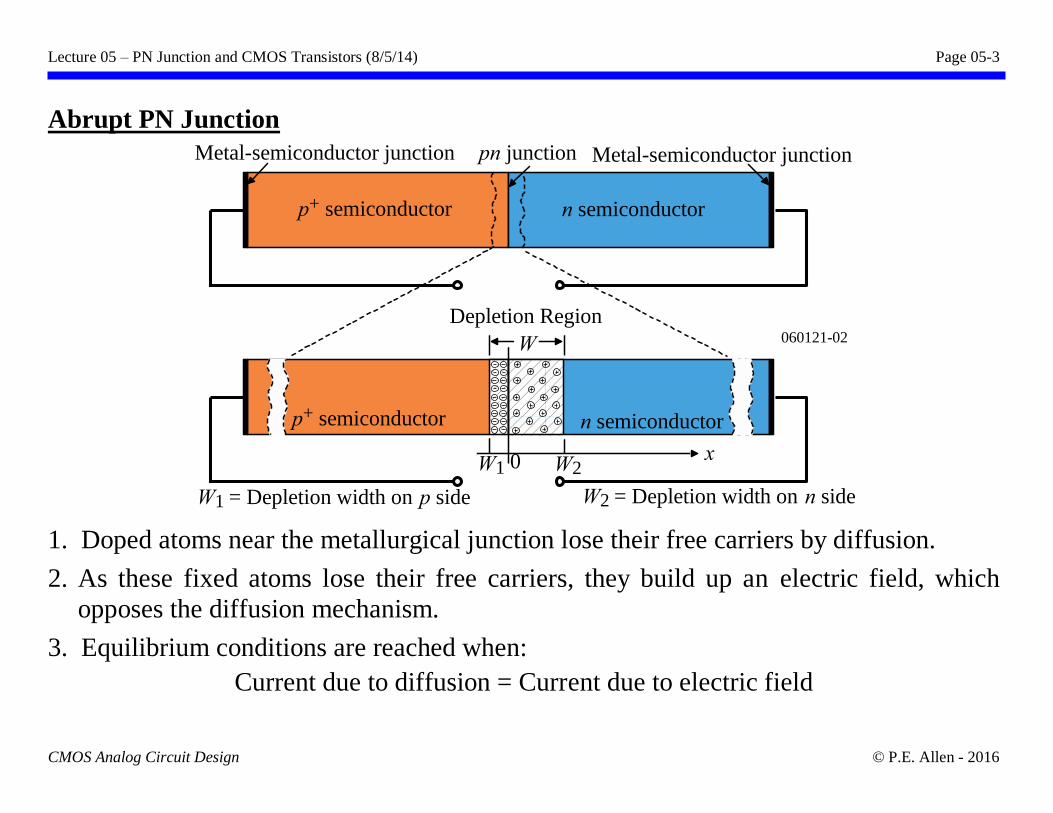
Abrupt PN Junction
1. Doped atoms near the metallurgical junction lose their free carriers by diffusion.
2. As these fixed atoms lose their free carriers, they build up an electric field, which
opposes the diffusion mechanism.
3. Equilibrium conditions are reached when:
Current due to diffusion = Current due to electric field
060121-02
p+ semiconductor n semiconductor
Metal-semiconductor junction pn junction Metal-semiconductor junction
p+ semiconductor n semiconductor
Depletion Region
W
xW1 0 W2
W1 = Depletion width on p side W2 = Depletion width on n side
Lecture 05 – PN Junction and CMOS Transistors (8/5/14) Page 05-4
CMOS Analog Circuit Design © P.E. Allen - 2016
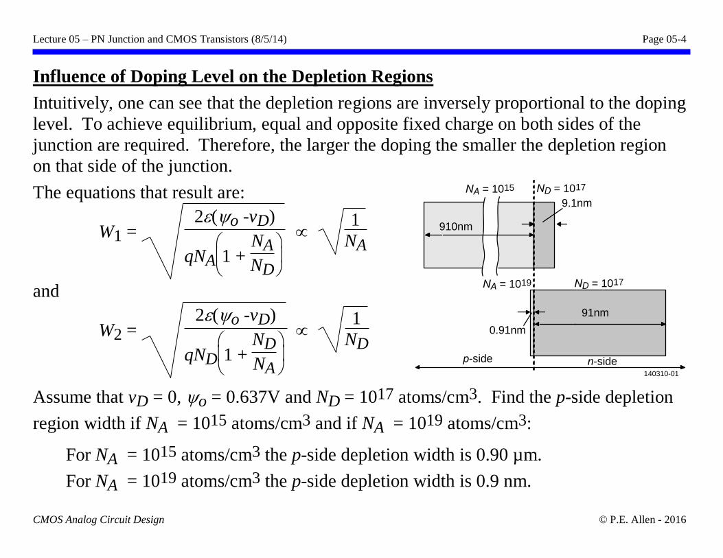
Influence of Doping Level on the Depletion Regions
Intuitively, one can see that the depletion regions are inversely proportional to the doping
level. To achieve equilibrium, equal and opposite fixed charge on both sides of the
junction are required. Therefore, the larger the doping the smaller the depletion region
on that side of the junction.
The equations that result are:
W1 = 2(o -vD)
qNA
1 + NA
ND
1
NA
and
W2 = 2(o -vD)
qND
1 + ND
NA
1
ND
Assume that vD = 0, o = 0.637V and ND = 1017 atoms/cm3. Find the p-side depletion
region width if NA = 1015 atoms/cm3 and if NA = 1019 atoms/cm3:
For NA = 1015 atoms/cm3 the p-side depletion width is 0.90 µm.
For NA = 1019 atoms/cm3 the p-side depletion width is 0.9 nm.
910nm
9.1nm
NA = 1015 ND = 1017
NA = 1019 ND = 1017
91nm
0.91nm
140310-01
p-side n-side
Lecture 05 – PN Junction and CMOS Transistors (8/5/14) Page 05-5
CMOS Analog Circuit Design © P.E. Allen - 2016
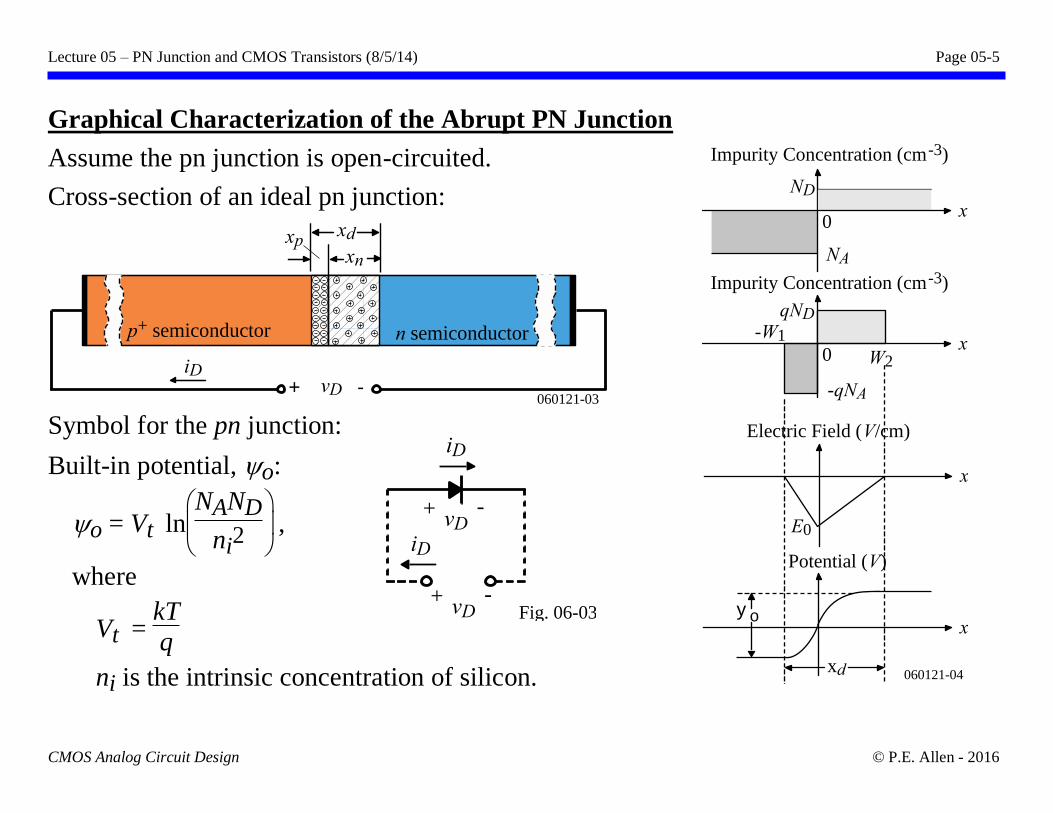
Graphical Characterization of the Abrupt PN Junction
Assume the pn junction is open-circuited.
Cross-section of an ideal pn junction:
Symbol for the pn junction:
Built-in potential, o:
o = Vt ln
NAND
ni2 ,
where
Vt = kT
q
ni is the intrinsic concentration of silicon.
060121-03
p+ semiconductor n semiconductor
xpxn
xd
+ -vD
iD
iD
vD+ -
vD+ -
iD
Fig. 06-03
060121-04
0
Impurity Concentration (cm-3)
ND
NA
x
0
Impurity Concentration (cm-3)
qND
x-W1
-qNA
W2
x
Electric Field (V/cm)
E0
x
Potential (V)
yo
xd
Lecture 05 – PN Junction and CMOS Transistors (8/5/14) Page 05-6
CMOS Analog Circuit Design © P.E. Allen - 2016
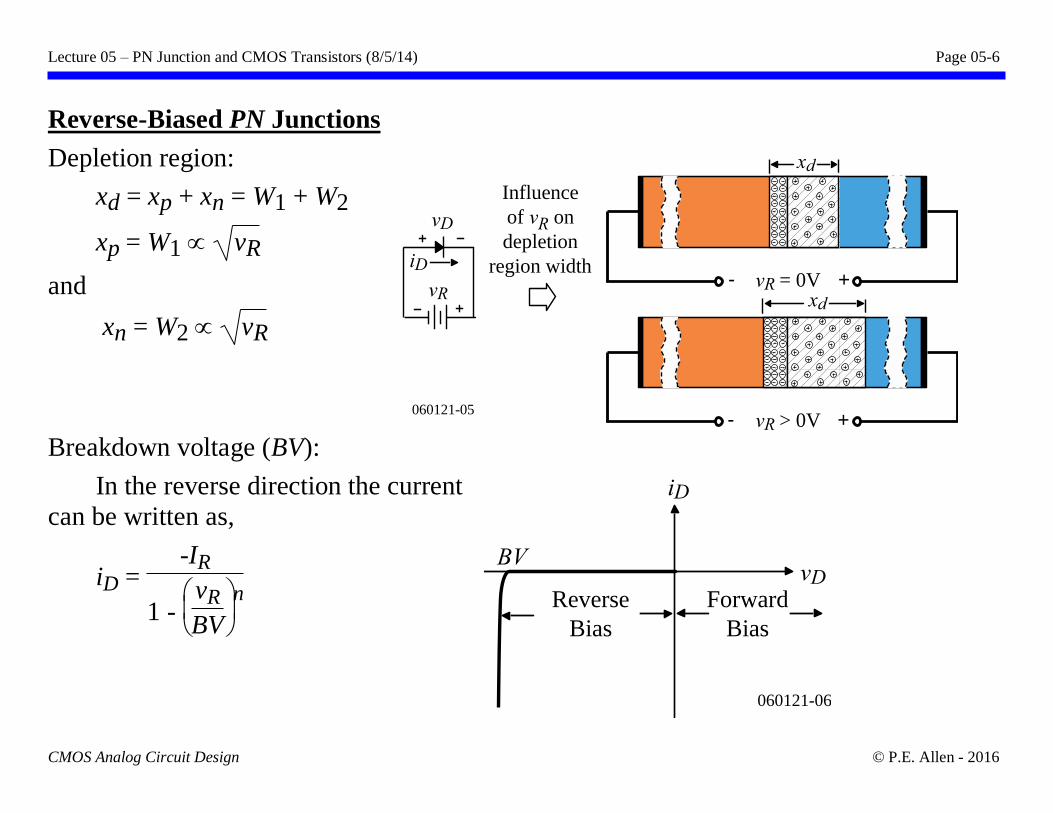
Reverse-Biased PN Junctions
Depletion region:
xd = xp + xn = W1 + W2
xp = W1 vR
and
xn = W2 vR
Breakdown voltage (BV):
In the reverse direction the current
can be written as,
iD = -IR
1 -
vR
BV
n
vD
iD
BV
060121-06
Reverse
Bias
Forward
Bias
vR
iD
vD
060121-05
+- vR = 0V
+- vR > 0V
xd
xd
Influence
of vR on
depletion
region width
Lecture 05 – PN Junction and CMOS Transistors (8/5/14) Page 05-7
CMOS Analog Circuit Design © P.E. Allen - 2016
Breakdown Voltage as a Function of Doping
It can be shown that†:
BV ≈ si(NA + ND)
2qNAND E
2max
where Emax = 3x10⁵ V/cm for silicon.
An example:
Assume that ND = 1017 atoms/cm3.
Find BV if NA = 1015 atoms/cm3 and if NA = 1019 atoms/cm3:
NA = 1015 atoms/cm3:
If NA << ND, then BV ≈ si
2qNA E
2max =
1.04x10-12·9x1010
2·1.6x10-19·1015 = 291V
NA = 1019 atoms/cm3:
If NA >> ND, then BV ≈ si
2qND E
2max =
1.04x10-12·9x1010
2·1.6x10-19·1017 = 2.91V
† P. Allen and D. Holberg, CMOS Analog Circuit Design, 3rd ed., Oxford University Press, 2012
Lecture 05 – PN Junction and CMOS Transistors (8/5/14) Page 05-8
CMOS Analog Circuit Design © P.E. Allen - 2016
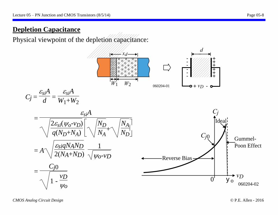
Depletion Capacitance
Physical viewpoint of the depletion capacitance:
Cj = siA
d =
siA
W1+W2
= siA
2si(o-vD)
q(ND+NA)
ND
NA+
NA
ND
= AsiqNAND
2(NA+ND)
1
o-vD
= Cj0
1 - vD
o
060204-01 + -vD
xd
W2W1
+-+-+-+-+-+-
d
060204-02
Cj0
Cj
vD0 yo
Reverse Bias
Ideal
Gummel-
Poon Effect
Lecture 05 – PN Junction and CMOS Transistors (8/5/14) Page 05-9
CMOS Analog Circuit Design © P.E. Allen - 2016
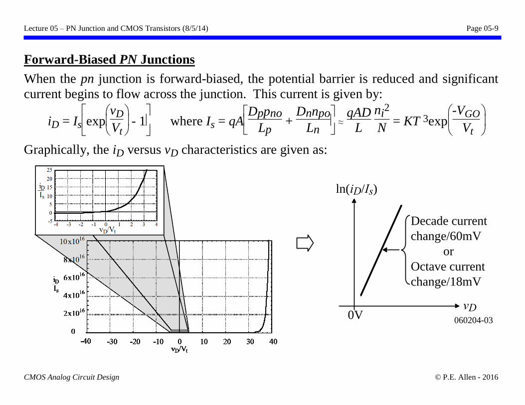
Forward-Biased PN Junctions
When the pn junction is forward-biased, the potential barrier is reduced and significant
current begins to flow across the junction. This current is given by:
iD = Is
exp
vD
Vt - 1 where Is = qA
Dppno
Lp +
Dnnpo
Ln ≈
qAD
L ni
2
N = KT 3exp
-VGO
Vt
Graphically, the iD versus vD characteristics are given as:
060204-03
ln(iD/Is)
vD
Decade current
change/60mV
or
Octave current
change/18mV
0V
Lecture 05 – PN Junction and CMOS Transistors (8/5/14) Page 05-10
CMOS Analog Circuit Design © P.E. Allen - 2016
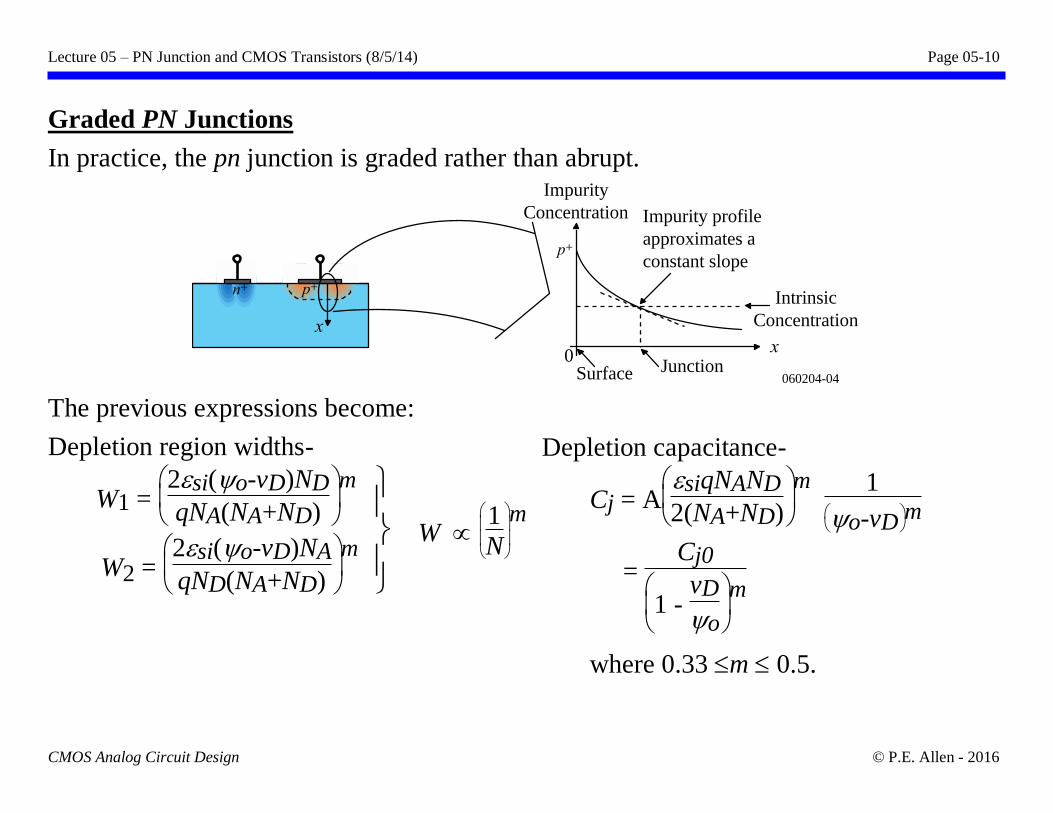
Graded PN Junctions
In practice, the pn junction is graded rather than abrupt.
The previous expressions become:
Depletion region widths-
W1 =
2si(o-vD)ND
qNA(NA+ND)
m
W2 =
2si(o-vD)NA
qND(NA+ND)
m W
1
N
m
060204-04
p+n+
xx
Impurity
Concentration
0Surface Junction
Impurity profile
approximates a
constant slopep+
Intrinsic
Concentration
Depletion capacitance-
Cj = A
siqNAND
2(NA+ND)
m
1
o-vD m
= Cj0
1 - vD
o
m
where 0.33 m 0.5.
Lecture 05 – PN Junction and CMOS Transistors (8/5/14) Page 05-11
CMOS Analog Circuit Design © P.E. Allen - 2016
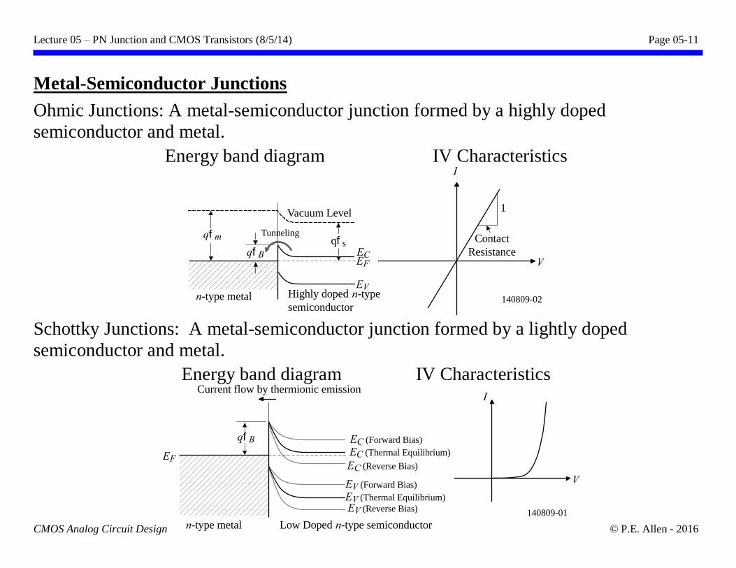
Metal-Semiconductor Junctions
Ohmic Junctions: A metal-semiconductor junction formed by a highly doped
semiconductor and metal.
Energy band diagram IV Characteristics
Schottky Junctions: A metal-semiconductor junction formed by a lightly doped
semiconductor and metal.
Energy band diagram IV Characteristics
I
V
qfB EC (Forward Bias)
EF
n-type metal Low Doped n-type semiconductor140809-01
EV (Forward Bias)
EC (Reverse Bias)
EV (Reverse Bias)
EC (Thermal Equilibrium)
EV (Thermal Equilibrium)
Current flow by thermionic emission
Contact
Resistance
1
I
V
Vacuum Level
qfm qfsqfB EC
EF
EV
Tunneling
n-type metal Highly doped n-type
semiconductor140809-02
Lecture 05 – PN Junction and CMOS Transistors (8/5/14) Page 05-12
CMOS Analog Circuit Design © P.E. Allen - 2016
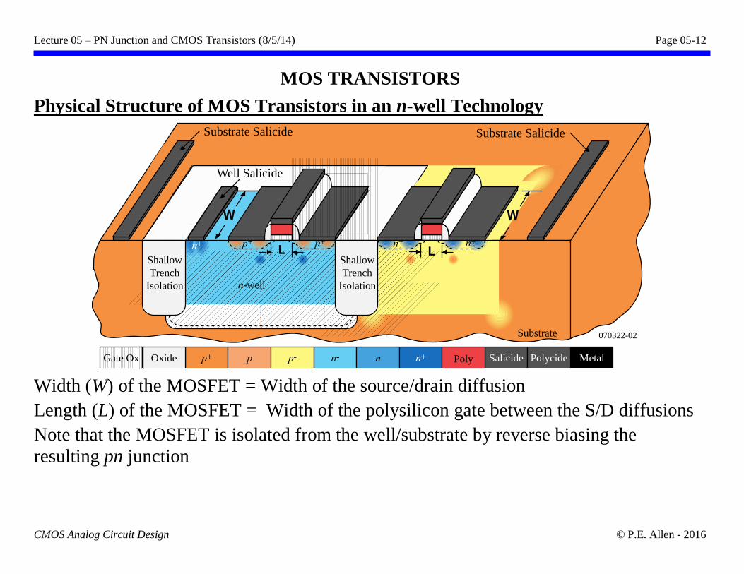
MOS TRANSISTORS
Physical Structure of MOS Transistors in an n-well Technology
Width (W) of the MOSFET = Width of the source/drain diffusion
Length (L) of the MOSFET = Width of the polysilicon gate between the S/D diffusions
Note that the MOSFET is isolated from the well/substrate by reverse biasing the
resulting pn junction
p+ p p- Metal Salicide n- n n+ Oxide Poly
070322-02
Polycide Gate Ox
n+
n-well
n+
p-well
n+
Substrate
n+
Substrate Salicide Substrate Salicide
Shallow
Trench
Isolation
Well Salicide
p+ p+
Shallow
Trench
Isolation
n+ n+
W
L
W
L
Lecture 05 – PN Junction and CMOS Transistors (8/5/14) Page 05-13
CMOS Analog Circuit Design © P.E. Allen - 2016
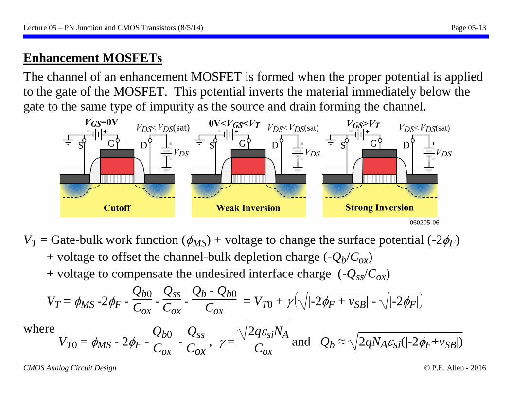
Enhancement MOSFETs
The channel of an enhancement MOSFET is formed when the proper potential is applied
to the gate of the MOSFET. This potential inverts the material immediately below the
gate to the same type of impurity as the source and drain forming the channel.
VT = Gate-bulk work function (MS) + voltage to change the surface potential (-2F)
+ voltage to offset the channel-bulk depletion charge (-Qb/Cox)
+ voltage to compensate the undesired interface charge (-Qss/Cox)
VT = MS -2F - Qb0
Cox -
Qss
Cox -
Qb - Qb0
Cox = VT0 +
|-2F + vSB| - |-2F|
where VT0 = MS - 2F -
Qb0
Cox -
Qss
Cox , =
2qsiNA
Cox and Qb ≈ 2qNAsi(|-2F+vSB|)
060205-06
VDS<VDS(sat)VGS=0V
S G DVDS
VDS<VDS(sat)0V<VGS<VT
S G DVDS
VDS<VDS(sat)
S G DVDS
VGS>VT
Cutoff Weak Inversion Strong Inversion
Lecture 05 – PN Junction and CMOS Transistors (8/5/14) Page 05-14
CMOS Analog Circuit Design © P.E. Allen - 2016
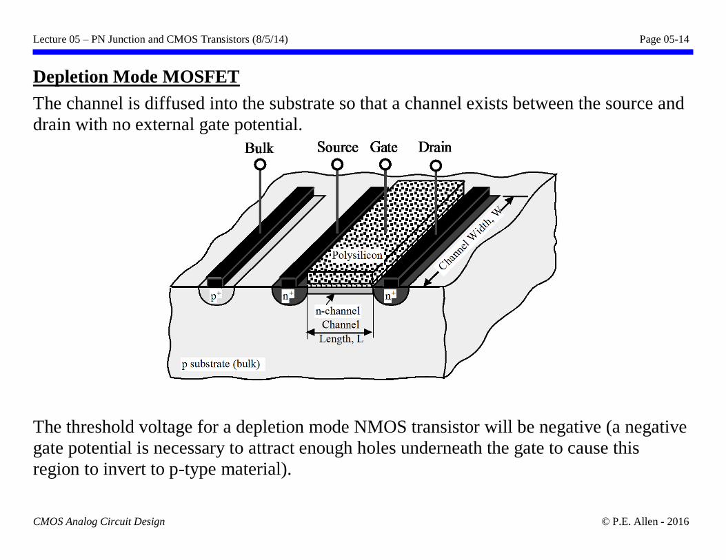
Depletion Mode MOSFET
The channel is diffused into the substrate so that a channel exists between the source and
drain with no external gate potential.
The threshold voltage for a depletion mode NMOS transistor will be negative (a negative
gate potential is necessary to attract enough holes underneath the gate to cause this
region to invert to p-type material).
Lecture 05 – PN Junction and CMOS Transistors (8/5/14) Page 05-15
CMOS Analog Circuit Design © P.E. Allen - 2016
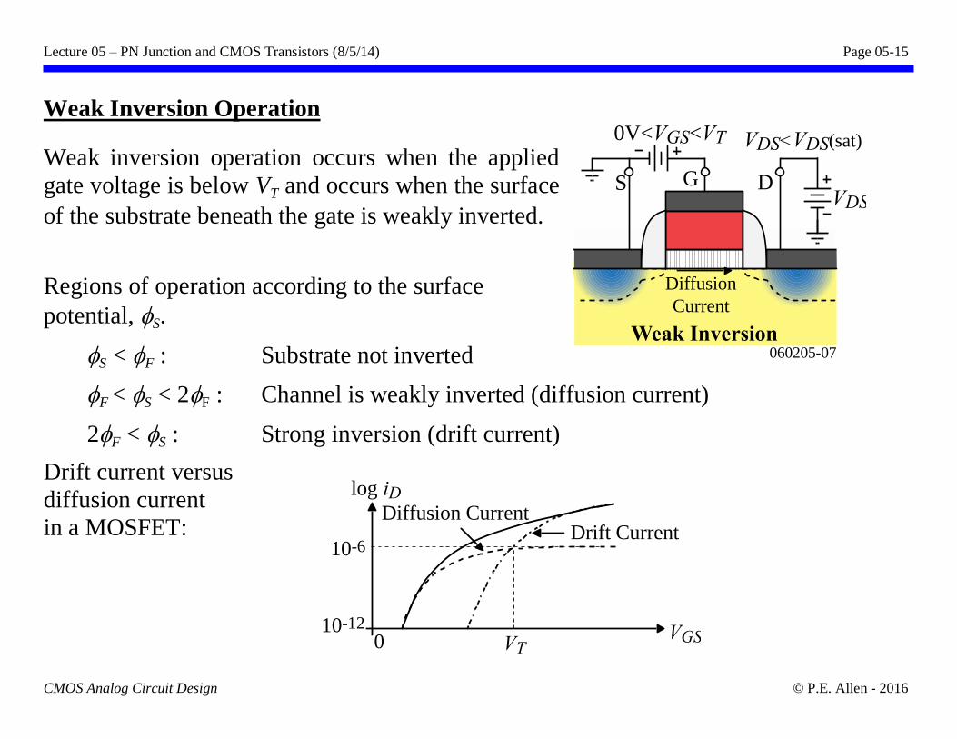
Weak Inversion Operation
Weak inversion operation occurs when the applied
gate voltage is below VT and occurs when the surface
of the substrate beneath the gate is weakly inverted.
Regions of operation according to the surface
potential, S.
S < F : Substrate not inverted
F < S < 2F : Channel is weakly inverted (diffusion current)
2F < S : Strong inversion (drift current)
Drift current versus
diffusion current
in a MOSFET:
060205-07
VDS<VDS(sat)0V<VGS<VT
S G DVDS
Weak Inversion
Diffusion
Current
log iD
10-6
10-12
0 VTVGS
Drift CurrentDiffusion Current
Lecture 05 – PN Junction and CMOS Transistors (8/5/14) Page 05-16
CMOS Analog Circuit Design © P.E. Allen - 2016
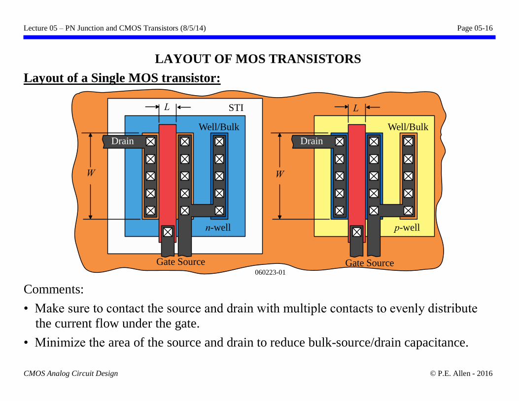
LAYOUT OF MOS TRANSISTORS
Layout of a Single MOS transistor:
Comments:
• Make sure to contact the source and drain with multiple contacts to evenly distribute
the current flow under the gate.
• Minimize the area of the source and drain to reduce bulk-source/drain capacitance.
060223-01
STI
n-well
W
L
Drain
Gate Source
Well/Bulk
p-well
Drain
Well/Bulk
W
L
Gate Source
Lecture 05 – PN Junction and CMOS Transistors (8/5/14) Page 05-17
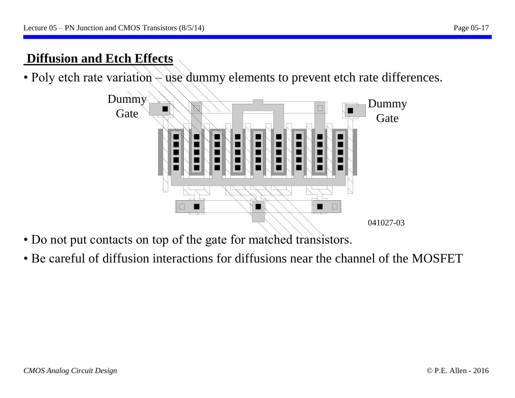
CMOS Analog Circuit Design © P.E. Allen - 2016
Diffusion and Etch Effects
• Poly etch rate variation – use dummy elements to prevent etch rate differences.
• Do not put contacts on top of the gate for matched transistors.
• Be careful of diffusion interactions for diffusions near the channel of the MOSFET
041027-03
Dummy
Gate
Dummy
Gate
Lecture 05 – PN Junction and CMOS Transistors (8/5/14) Page 05-18
CMOS Analog Circuit Design © P.E. Allen - 2016
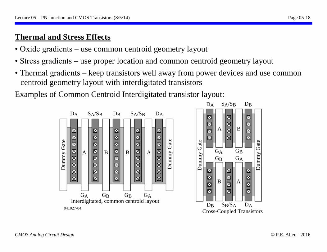
Thermal and Stress Effects
• Oxide gradients – use common centroid geometry layout
• Stress gradients – use proper location and common centroid geometry layout
• Thermal gradients – keep transistors well away from power devices and use common
centroid geometry layout with interdigitated transistors
Examples of Common Centroid Interdigitated transistor layout:
A B B A
Dum
my
Gat
e
Du
mm
y G
ate
DA SA/SB DB SA/SB DA
GA GAGB GBInterdigitated, common centroid layout
041027-04
Du
mm
y G
ate
Du
mm
y G
ate
BA
AB
SA/SBDA DB
GA GB
GB GA
SB/SADB DA
Cross-Coupled Transistors
Lecture 05 – PN Junction and CMOS Transistors (8/5/14) Page 05-19
CMOS Analog Circuit Design © P.E. Allen - 2016
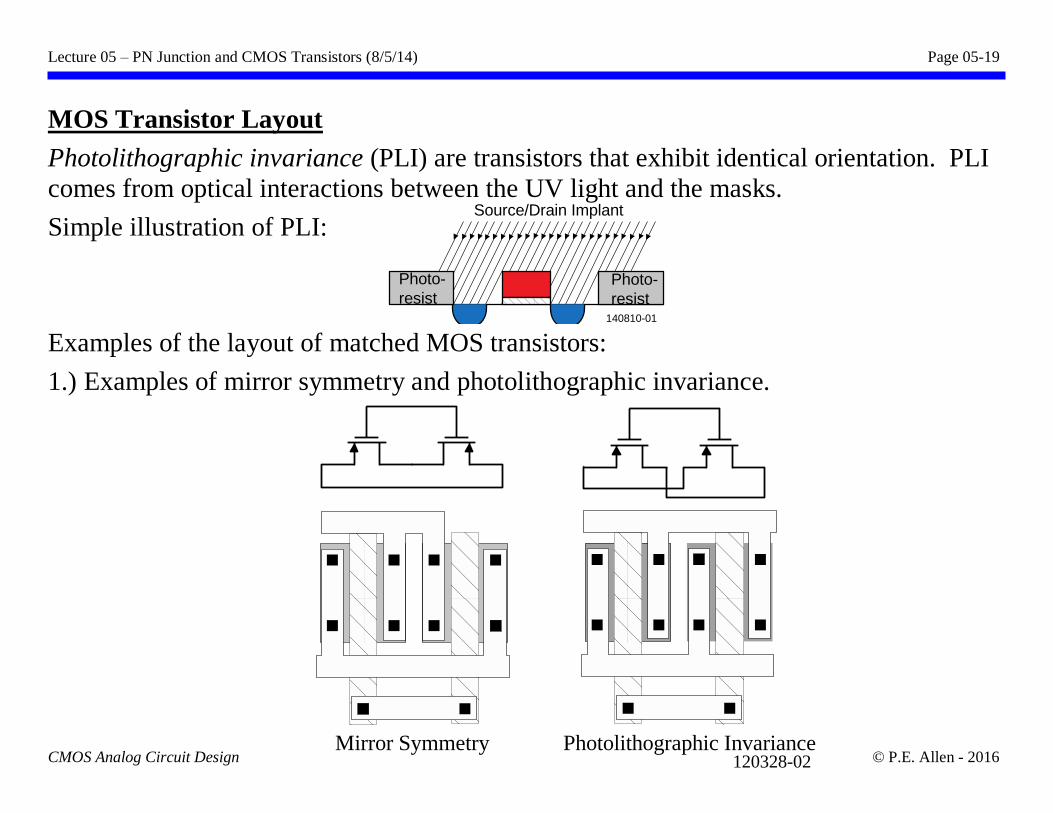
MOS Transistor Layout
Photolithographic invariance (PLI) are transistors that exhibit identical orientation. PLI
comes from optical interactions between the UV light and the masks.
Simple illustration of PLI:
Examples of the layout of matched MOS transistors:
1.) Examples of mirror symmetry and photolithographic invariance.
Mirror Symmetry Photolithographic Invariance120328-02
Photo-
resist
Photo-
resist
Source/Drain Implant
140810-01
Lecture 05 – PN Junction and CMOS Transistors (8/5/14) Page 05-20
CMOS Analog Circuit Design © P.E. Allen - 2016
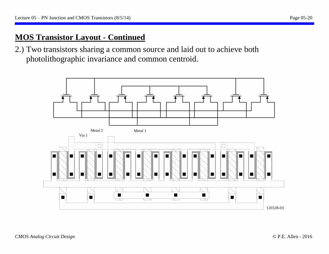
MOS Transistor Layout - Continued
2.) Two transistors sharing a common source and laid out to achieve both
photolithographic invariance and common centroid.
Metal 2
Via 1Metal 1
120328-03
Lecture 05 – PN Junction and CMOS Transistors (8/5/14) Page 05-21
CMOS Analog Circuit Design © P.E. Allen - 2016
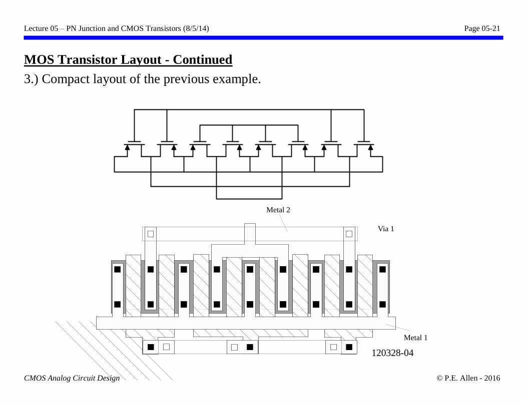
MOS Transistor Layout - Continued
3.) Compact layout of the previous example.
120328-04
Metal 2
Via 1
Metal 1
Lecture 05 – PN Junction and CMOS Transistors (8/5/14) Page 05-22
CMOS Analog Circuit Design © P.E. Allen - 2016
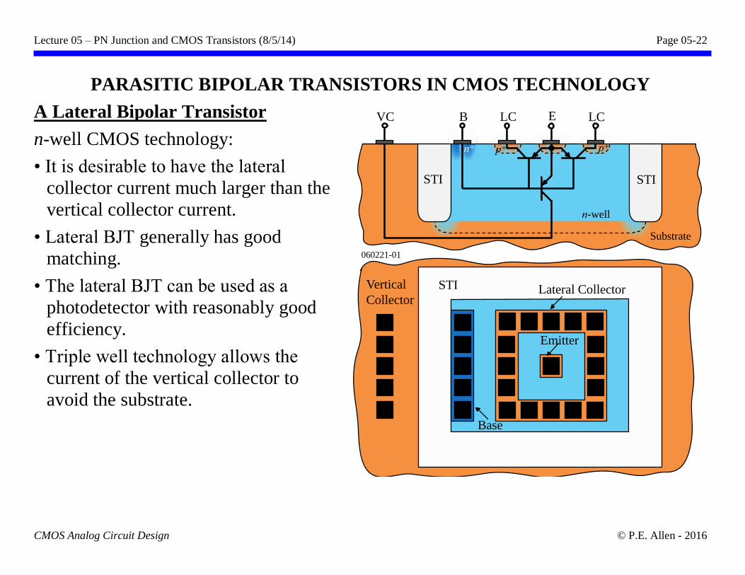
PARASITIC BIPOLAR TRANSISTORS IN CMOS TECHNOLOGY
A Lateral Bipolar Transistor
n-well CMOS technology:
• It is desirable to have the lateral
collector current much larger than the
vertical collector current.
• Lateral BJT generally has good
matching.
• The lateral BJT can be used as a
photodetector with reasonably good
efficiency.
• Triple well technology allows the
current of the vertical collector to
avoid the substrate.
060221-01
p+
n-well
n+
Substrate
E LCBVC
STI STI
LC
STI Lateral Collector
Emitter
Base
Vertical
Collector
p+ p+
Lecture 05 – PN Junction and CMOS Transistors (8/5/14) Page 05-23
CMOS Analog Circuit Design © P.E. Allen - 2016
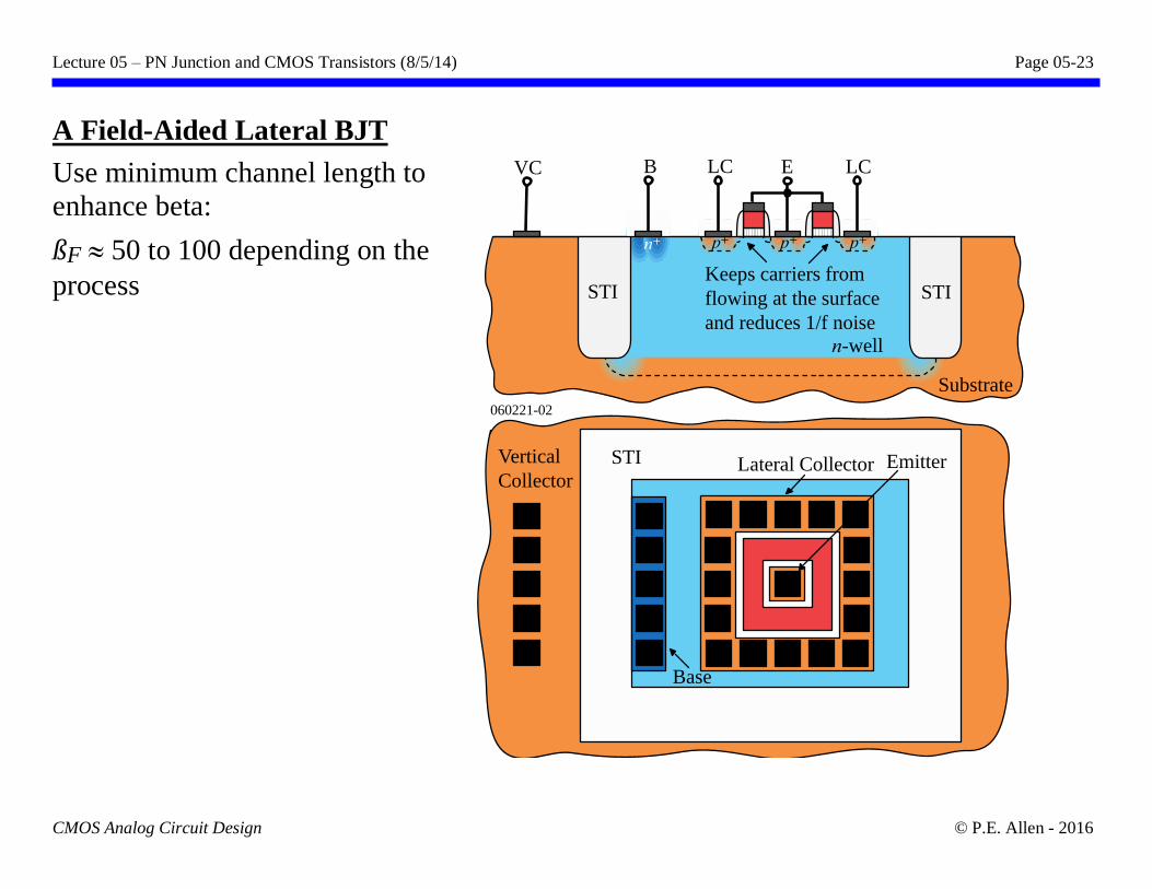
060221-02
p+
n-well
n+
Substrate
BVC
STI STI
LC
STI Lateral Collector Emitter
Base
Vertical
Collector
p+ p+p+
E LC
Keeps carriers from
flowing at the surface
and reduces 1/f noise
A Field-Aided Lateral BJT
Use minimum channel length to
enhance beta:
ßF 50 to 100 depending on the
process
Lecture 05 – PN Junction and CMOS Transistors (8/5/14) Page 05-24
CMOS Analog Circuit Design © P.E. Allen - 2016
HIGH VOLTAGE CMOS TRANSISTORS
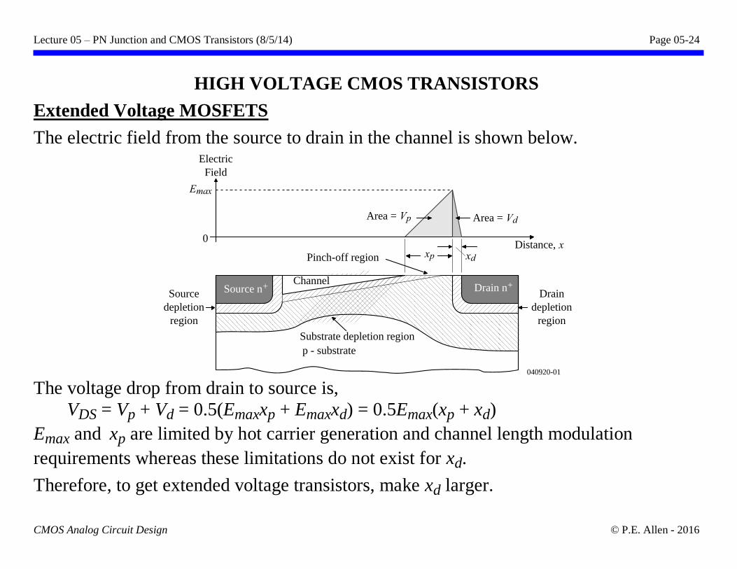
Extended Voltage MOSFETS
The electric field from the source to drain in the channel is shown below.
The voltage drop from drain to source is,
VDS = Vp + Vd = 0.5(Emaxxp + Emaxxd) = 0.5Emax(xp + xd)
Emax and xp are limited by hot carrier generation and channel length modulation
requirements whereas these limitations do not exist for xd.
Therefore, to get extended voltage transistors, make xd larger.
Source n+ Drain n+Channel
p - substrate
xp xd
Distance, x
Electric
Field
Emax
0
Drain
depletion
region
Substrate depletion region
Source
depletion
region
Area = Vp Area = Vd
040920-01
Pinch-off region
Lecture 05 – PN Junction and CMOS Transistors (8/5/14) Page 05-25
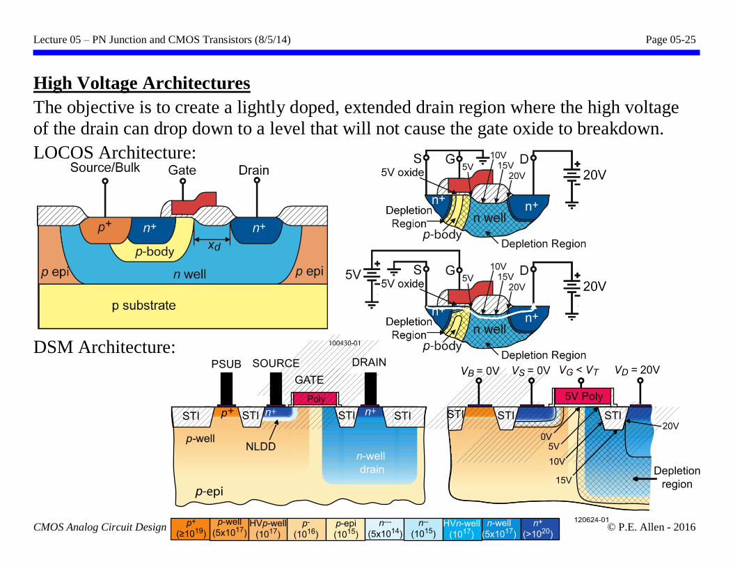
CMOS Analog Circuit Design © P.E. Allen - 2016
High Voltage Architectures
The objective is to create a lightly doped, extended drain region where the high voltage
of the drain can drop down to a level that will not cause the gate oxide to breakdown.
LOCOS Architecture:
DSM Architecture:
Lecture 05 – PN Junction and CMOS Transistors (8/5/14) Page 05-26
CMOS Analog Circuit Design © P.E. Allen - 2016
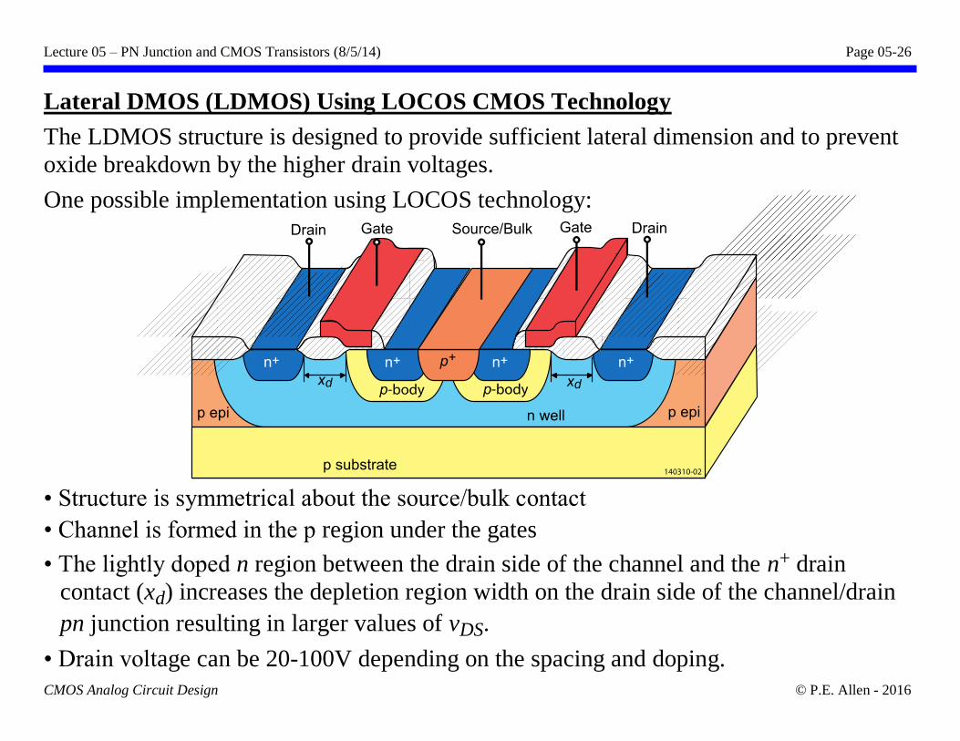
Lateral DMOS (LDMOS) Using LOCOS CMOS Technology
The LDMOS structure is designed to provide sufficient lateral dimension and to prevent
oxide breakdown by the higher drain voltages.
One possible implementation using LOCOS technology:
• Structure is symmetrical about the source/bulk contact
• Channel is formed in the p region under the gates
• The lightly doped n region between the drain side of the channel and the n+ drain
contact (xd) increases the depletion region width on the drain side of the channel/drain
pn junction resulting in larger values of vDS.
• Drain voltage can be 20-100V depending on the spacing and doping.
Lecture 05 – PN Junction and CMOS Transistors (8/5/14) Page 05-27
CMOS Analog Circuit Design © P.E. Allen - 2016
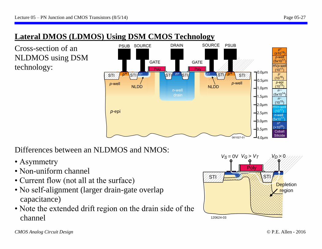
Lateral DMOS (LDMOS) Using DSM CMOS Technology
Cross-section of an
NLDMOS using DSM
technology:
Differences between an NLDMOS and NMOS:
• Asymmetry
• Non-uniform channel
• Current flow (not all at the surface)
• No self-alignment (larger drain-gate overlap
capacitance)
• Note the extended drift region on the drain side of the
channel 120624-03
Poly
VS = 0V
STISTI
Depletion
region
VG > VT VD > 0
Lecture 05 – PN Junction and CMOS Transistors (8/5/14) Page 05-28
CMOS Analog Circuit Design © P.E. Allen - 2016
SUMMARY
• pn junction usage in CMOS include:
- Electrical isolation, pn diodes, ESD protection, depletion capacitors
• Depletion region widths are inversely proportional to the doping
• Depletion region widths are proportional to the reverse bias voltage
• Ohmic metal-semiconductor junctions require a highly doped semiconductor
• MOSFETs can be:
- Enhancement – the applied gate voltage forms the channel
- Depletion – the channel is physically constructed in fabrication
• The threshold voltage of MOSFETs consists of the following components:
- Gate bulk work function (MS)
- Voltage to change the surface potential (-2F)
- Voltage to offset the channel-bulk depletion charge (-Qb/Cox)
- Voltage to compensate the undesired interface charge (-Qss/Cox)
• Weak inversion is MOSFET operation with the gate-source voltage less than the
threshold voltage
• Layout of the MOSFET is important to its performance and matching capabilities
• Extended drain regions lead to higher voltage capability MOSFETs


