Lect2 up370 (100329)
16
Lecture 370 – Testing of ADCs and Moderate Speed Nyquist ADCs (3/29/10) Page 370-1 CMOS Analog Circuit Design © P.E. Allen - 2010 LECTURE 370 – TESTING OF ADCS AND MODERATE SPEED NYQUIST ADCS LECTURE ORGANIZATION Outline • Introduction • Testing of ADCs • Serial ADCs • Successive approximation ADCs • Single-bit/stage pipeline ADCs • Iterative ADCs • Self calibration techniques • Summary CMOS Analog Circuit Design, 2 nd Edition Reference Pages 665-681 Lecture 370 – Testing of ADCs and Moderate Speed Nyquist ADCs (3/29/10) Page 370-2 CMOS Analog Circuit Design © P.E. Allen - 2010 TESTING OF ADCs Input-Output Test for an ADC Test Setup: N-bit ADC under test DAC with more resolution than ADC (N+2 bits) Digital Word Output (N bits) Fig.10.5-17 V in Σ - + V in ' Q n = V in -V in ' The ideal value of Q n should be within ±0.5LSB Can measure: • Offset error = constant shift above or below the 0 LSB line • Gain error = contant increase or decrease of the sawtooth plot as V in is increased • INL and DNL (see following page)
Transcript of Lect2 up370 (100329)

Lecture 370 – Testing of ADCs and Moderate Speed Nyquist ADCs (3/29/10) Page 370-1
CMOS Analog Circuit Design © P.E. Allen - 2010
LECTURE 370 – TESTING OF ADCS AND MODERATE SPEEDNYQUIST ADCS
LECTURE ORGANIZATIONOutline• Introduction• Testing of ADCs• Serial ADCs• Successive approximation ADCs• Single-bit/stage pipeline ADCs• Iterative ADCs• Self calibration techniques• SummaryCMOS Analog Circuit Design, 2nd Edition ReferencePages 665-681
Lecture 370 – Testing of ADCs and Moderate Speed Nyquist ADCs (3/29/10) Page 370-2
CMOS Analog Circuit Design © P.E. Allen - 2010
TESTING OF ADCsInput-Output Test for an ADCTest Setup:
N-bitADCunder test
DAC withmore resolution
than ADC(N+2 bits)
DigitalWord
Output(N bits)
Fig.10.5-17
Vin Σ-
+
Vin'Qn =
Vin-Vin'
The ideal value of Qn should be within ±0.5LSB
Can measure:• Offset error = constant shift above or below the 0 LSB line• Gain error = contant increase or decrease of the sawtooth plot as Vin is increased
• INL and DNL (see following page)

Lecture 370 – Testing of ADCs and Moderate Speed Nyquist ADCs (3/29/10) Page 370-3
CMOS Analog Circuit Design © P.E. Allen - 2010
Illustration of the Input-Output Test for a 4-Bit ADC
016
116
216
316
416
516
616
716
816
916
1016
1116
1216
1316
1416
1516
1616
0.0 LSB
0.5 LSB
1.0 LSB
1.5 LSB
2.0 LSB
-0.5 LSB
-1.0 LSB
-1.5 LSB
-2.0 LSB
Qua
ntiz
atio
n N
oise
(L
SBs)
Analog Input Normalized to VREF
+2LSBDNL
-2LSBINL
+2LSBINL
-2LSBDNL
Fig.10.5-18
Lecture 370 – Testing of ADCs and Moderate Speed Nyquist ADCs (3/29/10) Page 370-4
CMOS Analog Circuit Design © P.E. Allen - 2010
Measurement of Nonlinearity Using a Pure SinusoidThis test applies a pure sinusoid to the input of the ADC. Any nonlinearity will
appear as harmonics of the sinusoid. Nonlinear errors will occur when the dynamic range(DR) is less than 6N dB where N = number of bits.
N-bitADCunder test
Harmonicfree
sinusoid
Clock
Distortionor
SpectrumAnalyzer
t
|Vout(jω)|
ωfsig
SpectralOutput
1000
0
1000
1
1001
1
1111
1
Noise floordue to non-linearities
VREF
Fig. 10.5-19A
DR
N-bitDAC
with N+2bits
resolution
Vout(DAC)
Vout(DAC)
tVREF
Vin
Vin
fsig
Comments:• Input sinusoid must have less distortion that the required dynamic range• DAC must have more accuracy than the ADC
Lecture 370 – Testing of ADCs and Moderate Speed Nyquist ADCs (3/29/10) Page 370-5
CMOS Analog Circuit Design © P.E. Allen - 2010
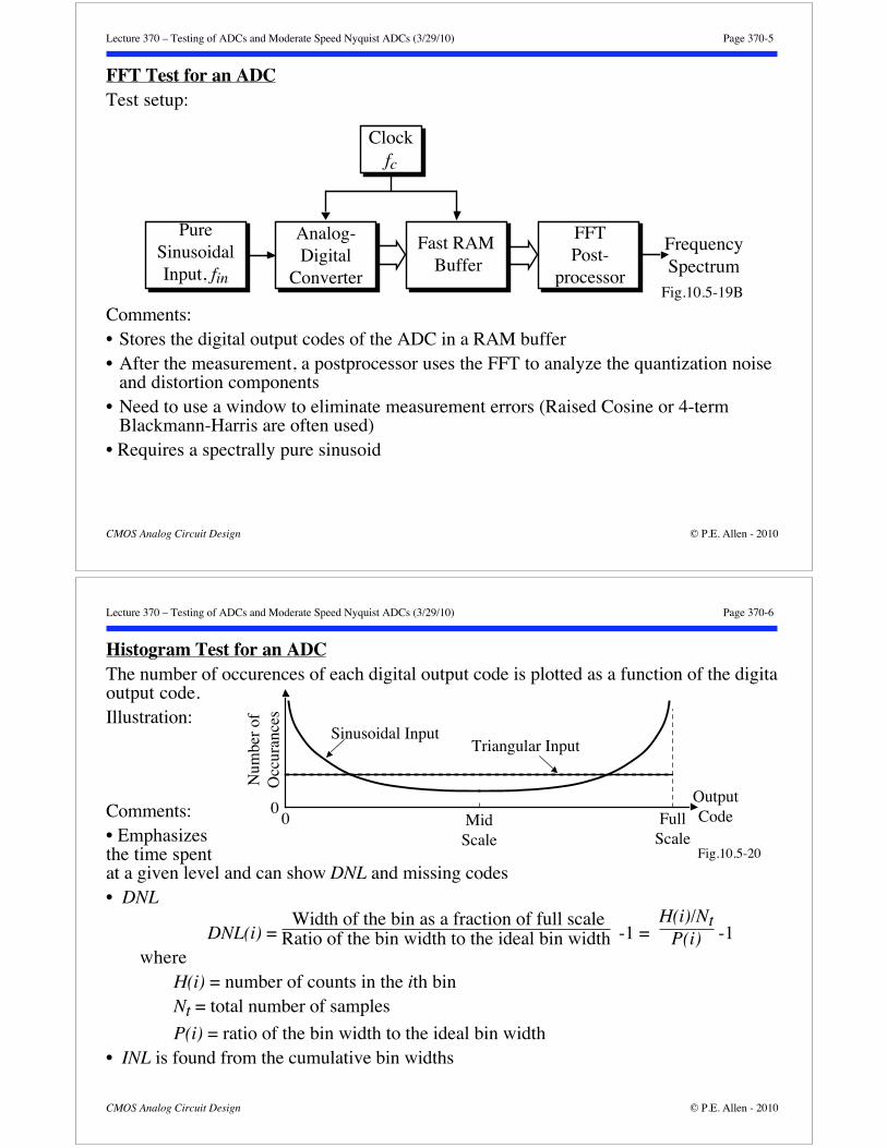
FFT Test for an ADCTest setup:
Analog-Digital
Converter
Fast RAM Buffer
FFTPost-
processor
PureSinusoidalInput, fin
Clockfc
FrequencySpectrum
Fig.10.5-19B
Comments:• Stores the digital output codes of the ADC in a RAM buffer• After the measurement, a postprocessor uses the FFT to analyze the quantization noise
and distortion components• Need to use a window to eliminate measurement errors (Raised Cosine or 4-term
Blackmann-Harris are often used)• Requires a spectrally pure sinusoid
Lecture 370 – Testing of ADCs and Moderate Speed Nyquist ADCs (3/29/10) Page 370-6
CMOS Analog Circuit Design © P.E. Allen - 2010
Histogram Test for an ADCThe number of occurences of each digital output code is plotted as a function of the digitaloutput code.Illustration:
Comments:• Emphasizesthe time spentat a given level and can show DNL and missing codes• DNL
DNL(i) = Width of the bin as a fraction of full scale
Ratio of the bin width to the ideal bin width -1 = H(i)/Nt
P(i) -1 where
H(i) = number of counts in the ith binNt = total number of samples
P(i) = ratio of the bin width to the ideal bin width• INL is found from the cumulative bin widths
0 MidScale
FullScale
Num
ber
of
Occ
uran
ces
Sinusoidal InputTriangular Input
OutputCode0
Fig.10.5-20
Lecture 370 – Testing of ADCs and Moderate Speed Nyquist ADCs (3/29/10) Page 370-7
CMOS Analog Circuit Design © P.E. Allen - 2010
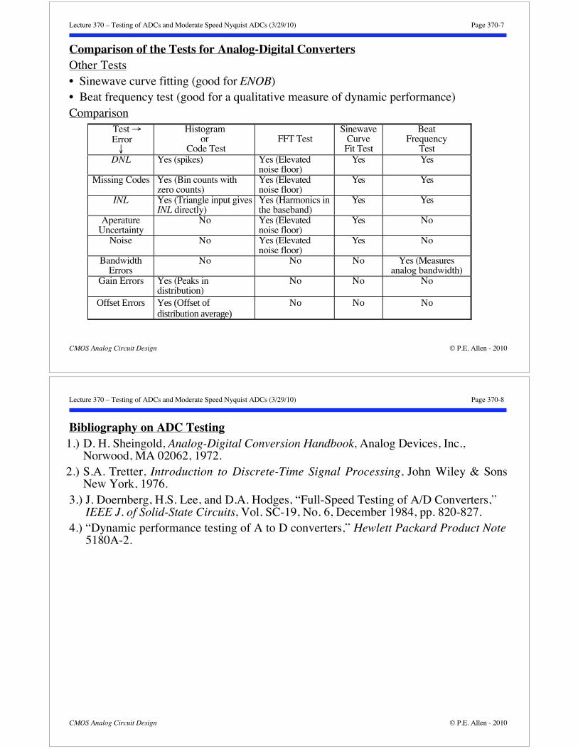
Comparison of the Tests for Analog-Digital ConvertersOther Tests• Sinewave curve fitting (good for ENOB)• Beat frequency test (good for a qualitative measure of dynamic performance)Comparison
Test Error
Histogramor
Code TestFFT Test
SinewaveCurve
Fit Test
BeatFrequency
TestDNL Yes (spikes) Yes (Elevated
noise floor)Yes Yes
Missing Codes Yes (Bin counts withzero counts)
Yes (Elevatednoise floor)
Yes Yes
INL Yes (Triangle input givesINL directly)
Yes (Harmonics inthe baseband)
Yes Yes
AperatureUncertainty
No Yes (Elevatednoise floor)
Yes No
Noise No Yes (Elevatednoise floor)
Yes No
BandwidthErrors
No No No Yes (Measuresanalog bandwidth)
Gain Errors Yes (Peaks indistribution)
No No No
Offset Errors Yes (Offset ofdistribution average)
No No No
Lecture 370 – Testing of ADCs and Moderate Speed Nyquist ADCs (3/29/10) Page 370-8
CMOS Analog Circuit Design © P.E. Allen - 2010
Bibliography on ADC Testing1.) D. H. Sheingold, Analog-Digital Conversion Handbook, Analog Devices, Inc.,
Norwood, MA 02062, 1972.2.) S.A. Tretter, Introduction to Discrete-Time Signal Processing, John Wiley & Sons
New York, 1976.3.) J. Doernberg, H.S. Lee, and D.A. Hodges, “Full-Speed Testing of A/D Converters,”
IEEE J. of Solid-State Circuits, Vol. SC-19, No. 6, December 1984, pp. 820-827.4.) “Dynamic performance testing of A to D converters,” Hewlett Packard Product Note
5180A-2.
Lecture 370 – Testing of ADCs and Moderate Speed Nyquist ADCs (3/29/10) Page 370-9
CMOS Analog Circuit Design © P.E. Allen - 2010
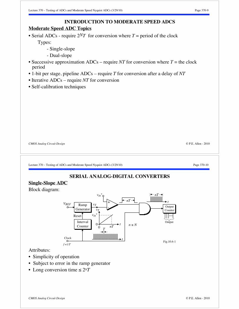
INTRODUCTION TO MODERATE SPEED ADCSModerate Speed ADC Topics
• Serial ADCs - require 2NT for conversion where T = period of the clockTypes:
- Single-slope- Dual-slope
• Successive approximation ADCs – require NT for conversion where T = the clockperiod
• 1-bit per stage, pipeline ADCs – require T for conversion after a delay of NT• Iterative ADCs – require NT for conversion• Self-calibration techniques
Lecture 370 – Testing of ADCs and Moderate Speed Nyquist ADCs (3/29/10) Page 370-10
CMOS Analog Circuit Design © P.E. Allen - 2010
SERIAL ANALOG-DIGITAL CONVERTERSSingle-Slope ADCBlock diagram:
RampGenerator vT
vT
vin*
vin*
nTt0
0
VREF
IntervalCounter
t
t
Clock
f =1/T
T
OutputCounter
nT
nT
Output
Reset
+-
Fig.10.6-1
n ≤ N
Attributes:• Simplicity of operation• Subject to error in the ramp generator• Long conversion time 2NT
Lecture 370 – Testing of ADCs and Moderate Speed Nyquist ADCs (3/29/10) Page 370-11
CMOS Analog Circuit Design © P.E. Allen - 2010
Dual-Slope ADCBlock diagram: Waveforms:
PositiveIntegrator
1
2
DigitalControl
Counter
vin*
-VREF
vint
Vth
CarryOutput Binary
Output
+-
Fig.10.6-2
Operation:1.) Initially vint = 0 and vin is sampled and held (vIN* > 0).2.) Reset the positive integrator by integrating a positive voltage until vint (0) = Vth.
3.) Integrate vin* for NREF clock cycles to get,
vint(t1) = K 0
NREFT
vin* dt + vint(0) = KNREFTvin* + Vth4.) After NREF counts, the carry output of the counter closes switch 2 and-VREF isapplied to the positive integrator. The output of the integrator at t = t1+t2 is,
vint(t1+t2) = vint(t1)+K t1
NoutT
( VREF)dt =Vth KNREFTvin*+Vth -KNoutTVREF = Vth
5.) Solving for Nout gives, Nout = NREF (vin*/VREF)
Comments: Conversion time 2(2N)T and the operation is independent of Vth and K.
vin
VREF+Vth
Vth0
0t
vin'''
vin''
vin'
Reset t0(start)
t1 = NREFT
t2' t2''t2'''
t2= NoutT
NREFT
Fig.10.6-3
vin''' > vin'' > vin'.
Lecture 370 – Testing of ADCs and Moderate Speed Nyquist ADCs (3/29/10) Page 370-12
CMOS Analog Circuit Design © P.E. Allen - 2010
SUCCESSIVE APPROXIMATION ANALOG-DIGITAL CONVERTERSIntroductionSuccessive Approximation Algorithm:1.) Start with the MSB bit and work toward the LSB bit.2.) Guess the MSB bit as 1.3.) Apply the digital word 10000.... to a DAC.4.) Compare the DAC output with the sampled analog input voltage.5.) If the DAC output is greater, keep the guess of 1. If the DAC output is less, change
the guess to 0.6.) Repeat for the next MSB.
vguessVREF
0.50VREF
00 1 2 3 4 5 6
tT
Fig.10.7-2
0.75VREF
0.25VREF

Lecture 370 – Testing of ADCs and Moderate Speed Nyquist ADCs (3/29/10) Page 370-13
CMOS Analog Circuit Design © P.E. Allen - 2010
Block Diagram of a Successive Approximation ADC†
OutputRegister
Digital-AnalogConverter
Conditional
ShiftRegister Clock
Output
VREF
Vin*+-
Comparator
Fig.10.7-1 Gates
† R. Hnatek, A User's Handbook of D/A and A/D Converters, John Wiley and Sons, Inc., New York, NY, 1976.
Lecture 370 – Testing of ADCs and Moderate Speed Nyquist ADCs (3/29/10) Page 370-14
CMOS Analog Circuit Design © P.E. Allen - 2010
5-Bit Successive Approximation ADC
AnalogSwitch
5
0 1FF5
R RD S
LSB
G5
AnalogSwitch
4
0 1FF4
R RD S
G4
VREF
LSB
AnalogSwitch
3
0 1FF3
R RD S
G3
AnalogSwitch
2
0 1FF2
R RD S
G2
AnalogSwitch
1
0 1FF1
R RD S
G1
MSB
5-bit Digital-Analog Converter
MSB
Shift Register
1SR5
1SR4SR3SR2SR1
111
Delay
-1
+ -
AnalogIn
Comp-arator
vIA vOA
Gate
Delay
Clock pulses
Start pulseThe delay allows for the circuit transients to settle before the comparator output is sampled. Fig.10.7-3

Lecture 370 – Testing of ADCs and Moderate Speed Nyquist ADCs (3/29/10) Page 370-15
CMOS Analog Circuit Design © P.E. Allen - 2010
m-Bit Voltage-Scaling, k-Bit Charge-Scaling Successive Approximation ADCOperation:1.) With the two SFswitches closed, allcapacitors are paralleledand connected to Vin*
which autozeros thecomparator offsetvoltage.2.) With all capacitorsstill in parallel, a suc-cessive approximationsearch is performed tofind the resistor segmentin which the analogsignal lies.3.) Finally, a successiveapproximation search is performed on charge scaling subDAC to establish the analogoutput voltage.
Ck =2k-1C
Sk-1,A
SBSF
Bus A
Bus B
Sk,A
Sk,B
Ck-1=2k-2C
Sk-1,B
C2=2C
C1=C
C
Vin*
S2A
S2B
S1A
S1B
m-to-2m Decoder A
m-to-2m Decoder BVREF
R1 R2 R3 R2m-2 R2m-1 R2m
m-MSB bits
m-MSB bits
m-bit, MSB voltagescaling subDAC
k-bit, LSB chargescaling subDAC
+-SF
m-MSB bits
ClockCapacitor Switches
(m+k) bit output of ADC Start
Successive approximationregister & switch control logic
Fig.10.7-4
Lecture 370 – Testing of ADCs and Moderate Speed Nyquist ADCs (3/29/10) Page 370-16
CMOS Analog Circuit Design © P.E. Allen - 2010
Voltage-Scaling, Charge-Scaling Successive Approximation ADC - ContinuedAutozero Step
Removes the influence of the offset voltage of thecomparator.
The voltage across the capacitor is given as,vC = Vin* - VOS
Successive Approximation Search on the Resistor StringThe voltage at the comparator input is
vcomp = VRi - Vin*
If vcomp > 0, then VRi > Vin*, if vcomp < 0, then VRi < Vin*
Successive Approximation Search on the Capacitor SubDACThe input to the comparator is written as,
vcomp = (VRi+1 - V *in)
Ceq2kC + (VRi - V *
in) 2kC-Ceq
2kCHowever, VRi+1 = VRi + 2-mVREFCombining gives,
vcomp = (VRi + 2-mVREF -V *IN)
Ceq2kC + (VRi-V *
IN) 2kC-Ceq
2kC
= VRi - V *IN + 2-mVREF Ceq2kC
+-
Vin*+
-VOS
+ -vC
2kC
VOS
Fig.10.7-5
+
-VRi=V'REF
vcomp
2kC
Busses A and B
V*in
+ -
Fig.10.
Fig.10.7-6
+
-
2-mVREF
VRi=V'REF
vcompCeq.
2kC - Ceq.
Bus A
Bus B
V*in
VRi+1
+ -
V*in
+ -+
-

Lecture 370 – Testing of ADCs and Moderate Speed Nyquist ADCs (3/29/10) Page 370-17
CMOS Analog Circuit Design © P.E. Allen - 2010
SINGLE-BIT/STAGE, PIPELINE ANALOG-DIGITAL CONVERTERSSingle-Bit/Stage Pipeline ADC Architecture
Operation:• Each stage multipliesits input by 2 and adds orsubtracts VREF dependingupon the sign of the input.• i-th stage,
Vi = 2Vi-1 - biVREF
where bi is given as
bi = +1 if Vi-1>0-1 if Vi-1<0
+ -
Σ z-12
±1Vin*
VREF
+ -
ΣVi-12
±1z-1
+ -
ΣVi2
±1z-1
+ -
i-th stage
MSB LSB
Fig.10.7-9Stage 1 Stage 2 Stage N
z-1
Vi/VREF1.0
-1.0
0 0.5 1.0-1.0 -0.50
bi+1=+1
bi+1=-1
bi = -1 bi = +1
Vi-1/VREF
[bi,bi+1] [0,0] [0,1] [1,0] [1,1] Fig.10.7-10
Implementation:
Lecture 370 – Testing of ADCs and Moderate Speed Nyquist ADCs (3/29/10) Page 370-18
CMOS Analog Circuit Design © P.E. Allen - 2010
Example 370-1 - Illustration of the Operation of the Pipeline ADCAssume that the sampled analog input to a 4-bit pipeline analog-digital converter is 2.00V. If VREF is equal to 5 V, find the digital output word and the analog equivalent voltage.Solution
Stage No. Input to the ith stage, Vi-1 Vi-1 > 0? Bit i1 2V Yes 12 (2V·2) - 5 = -1V No 03 (-1V·2) + 5 = 3V Yes 14 (3V·2) - 5 = 1V Yes 1
-1
-0.8
-0.6
-0.4
-0.2
0
0.2
Stag
e O
uput
s no
rmal
ized
to V
0.4
0.6
0.8
1
-1 -0.8 -0.6 -0.4 -0.2 0 0.2 0.4 0.6 0.8 1
REF
Stage 1
Stage 2
Stage 3
Stage 4
V in*/V REF
Illustration:
Vanalog = 512
14 +
18 +
116
= 5(0.4375) = 2.1875
where bi = +1 if the ith-bit is 1and bi = -1 if the ith bit is 0

Lecture 370 – Testing of ADCs and Moderate Speed Nyquist ADCs (3/29/10) Page 370-19
CMOS Analog Circuit Design © P.E. Allen - 2010
Achieving the High Speed Potential of the Pipeline ADCIf shift registers are used to store the output bits and align them in time, the pipeline ADCcan output a digital word at every clock cycle with a latency of NT.Illustration:
+ -
Σ z-12
±1Vin*
VREF
+ -
ΣVi-12
±1z-1
+ -
ΣVi2
±1z-1
+ -
i-th stage
MSB
LSB
Fig.10.7-9BStage 1 Stage 2 Stage N
z-1
SR
SR
SR
SR
i-th Bit
SR
SR
SR
MSB-1SR
Digital Ouput Word
Lecture 370 – Testing of ADCs and Moderate Speed Nyquist ADCs (3/29/10) Page 370-20
CMOS Analog Circuit Design © P.E. Allen - 2010
Errors in the Pipeline ADCTypes of errors:• Gain errors – x2 amplifier or summing junctions• Offset errors – comparators or summing junctionsIllustration of errors:
060927-04
2ΔAi
Vo/VREF
Vi/VREF2ΔAi
1
1
-1
-1
00
2VOSi
Vo/VREF
Vi/VREF1
1
-1
-1
00
System offset error, VOSi.
2VOSi
Vo/VREF
Vi/VREF1
1
-1
-1
00
Comparator offset error, VOCi.2VOCi
Gain error, Ai.
An error will occur if the output voltage of one stage exceeds ±VREF (saturates).

Lecture 370 – Testing of ADCs and Moderate Speed Nyquist ADCs (3/29/10) Page 370-21
CMOS Analog Circuit Design © P.E. Allen - 2010
Digital Error CorrectionIn the previous slide, we noted that if the analog output to the next stage exceeds ±VREFthat an error occurs. This error can be detected by adding one more bit to the followingstage for the purposes of detecting the error.Illustration (2nd bit not used for error correction):
060930-01
VREF
VREF
-VREF
-VREF
Vout(i)
Vin(i)
0 0 1 1VREF
VREF
-VREF
-VREF
Vout(i)
Vin(i)
[00] [01] [10] [11]
1
0
00 01 10 11
11
10
01
00
[0000][0001][0010][0011][0100][0101][0110][0111][1000][1001][1010][1011][1100][1101][1110][1111]
InputRange
for nextStage
InputRange
for nextStage
Input/output characteristics of a 1-bit stage Input/output characteristics of a 2-bit stage
Lecture 370 – Testing of ADCs and Moderate Speed Nyquist ADCs (3/29/10) Page 370-22
CMOS Analog Circuit Design © P.E. Allen - 2010
Digital Error Correction – ContinuedIf the gain of 4 amplifier is reduced back to 2, the input/output characteristics of the 2-bitstage become:
060930-02
VREF
VREF
-VREF
-VREF
Vout(i)
Vin(i)
00 01 10 11
10
01
[0001]
[0010]
[0101]
[0110]
[1001]
[1010]
[1101]
[1110]
InputRangefor nextStage
11
00
The output bits can be used to determine the error. If these bits are 00, then 0.5LSB mustbe added to get the correct digital output. If the bits are 11, then 0.5LSB must besubtracted to get the correct digital output.

Lecture 370 – Testing of ADCs and Moderate Speed Nyquist ADCs (3/29/10) Page 370-23
CMOS Analog Circuit Design © P.E. Allen - 2010
Modified Digital Error Correction (1.5 bits per stage)In the previous slide, it was necessary sometimes to perform digital subtraction which isnot easy to implement. To avoid this problem, a 0.5LSB shift has been added to theinput/output characteristic resulting in the following.
VREF
VREF
-VREF
-VREF
Vout(i)
Vin(i)
00 01 10 11
InputRangefor nextStage
060930-03
VREF
VREF
-VREF
-VREF
Vout(i)
Vin(i)
00 01 10
[0000]
[0001]
[0100][0101]
[1000][1001]
[1010]
[0010]
-VREF4
VREF4
00
01
1011
00
01
10
[0110]
[0000]
[0001]
[0100][0101]
[1000][1001][1010]
[0010]
[0110]
[1100][1101]
Movement of all comparator thresholdsto the right by 0.5LSB.
Removal of the comparator at 0.75LSB.
InputRangefor nextStage
To obtain code 11 out of the stage after correction, the correction logic must incrementthe output of the stage.To obtain code 00 from this stage after correction, the correction logic need do nothing.Therefore, only two comparators are needed to produce outputs of (00, 01, 10) as shownon the right-hand characteristic.
Lecture 370 – Testing of ADCs and Moderate Speed Nyquist ADCs (3/29/10) Page 370-24
CMOS Analog Circuit Design © P.E. Allen - 2010
How Does the 1.5 Bit Stage Correct Offset Errors?Consider a ±0.25VREF comparator offset shift in the input-output characteristics of the1.5 bit stage.
061001-01
VREF
Vout(i)
Vin(i)InputRangefor nextStage
VREF
10 14
24
341 3
424
14
----
1
0
0.5
-0.5
-1
Comparator shiftfrom 0.25VREFto 0VREF
VREF
Vout(i)
Vin(i)InputRangefor nextStage
VREF
10 14
24
341 3
424
14
----
1
0
0.5
-0.5
-1
Comparator shiftfrom 0.25VREFto 0.5VREF
When the shift is to the left, the comparator will not be in error until the shift is greaterthan 0.25 VREF. This is because the comparator thresholds were shifted to the right by0.5 VREF.
When the shift is to the right, the input to the next stage will be greater than 0.50VREF.This will cause the output code 10 which indicates that the digital word should beincremented by 1 bit.
The range of correction ±VREF /2B+1 where B is the number of bits per stage.

Lecture 370 – Testing of ADCs and Moderate Speed Nyquist ADCs (3/29/10) Page 370-25
CMOS Analog Circuit Design © P.E. Allen - 2010
Implementation of the 1.5 Bit Stage
061001-03
+
−
vin φ1
C
φ2
VREFφ1
C
φ24
φ1
+
−
vin φ1
C
φ2
VREFφ1
C
φ24
φ1
−
Sub-ADC
+
− φ2
φ1
φ1
φ1
φ2
VREF
VREF
MultiplyingSub-DAC
vout
C Cvin ≥ VREF
4+
vin < VREF
4−
1 if
1 if
φ1
The multiplying Sub-DAC must implement the following equation:
Vout =
2·vin - VREF2·vin2·vin + VREF
if vin > VREF/4if -VREF/4 vin VREF/4if vin < -VREF/4
Lecture 370 – Testing of ADCs and Moderate Speed Nyquist ADCs (3/29/10) Page 370-26
CMOS Analog Circuit Design © P.E. Allen - 2010
Example 370-2 - Accuracy requirements for a 5-bit pipeline ADCShow that if Vin = VREF, that the pipeline ADC will have an error in the 5th bit if the gainof the first stage is 2-(1/8) =1.875 which corresponds to when an error will occur. Showthe influence of Vin on this result for Vin of 0.65VREF and 0.22VREF.
SolutionFor Vin = VREF, we get the results shown below. The input to the fifth stage is 0V
which means that the bit is uncertain. If A1 was slightly less than 1.875, the fifth bitwould be 0 which is in error. This result assumes that all stages but the first are ideal.
i Vi(ideal) Bit i (ideal) Vi(A1=1.875) Bit i (A1=1.875)1 1 1 1.000 12 1 1 0.875 13 1 1 0.750 14 1 1 0.500 15 1 1 0.000 ?
Now let us repeat the above results for Vin = 0.65VREF. The results are shown below.i Vi(ideal) Bit i (ideal) Vi(A1=1.875) Bit i (A1=1.875)1 +0.65 1 0.6500 12 +0.30 1 0.2188 13 -0.40 0 -0.5625 04 +0.20 1 -0.1250 05 -0.60 0 0.7500 1
Lecture 370 – Testing of ADCs and Moderate Speed Nyquist ADCs (3/29/10) Page 370-27
CMOS Analog Circuit Design © P.E. Allen - 2010
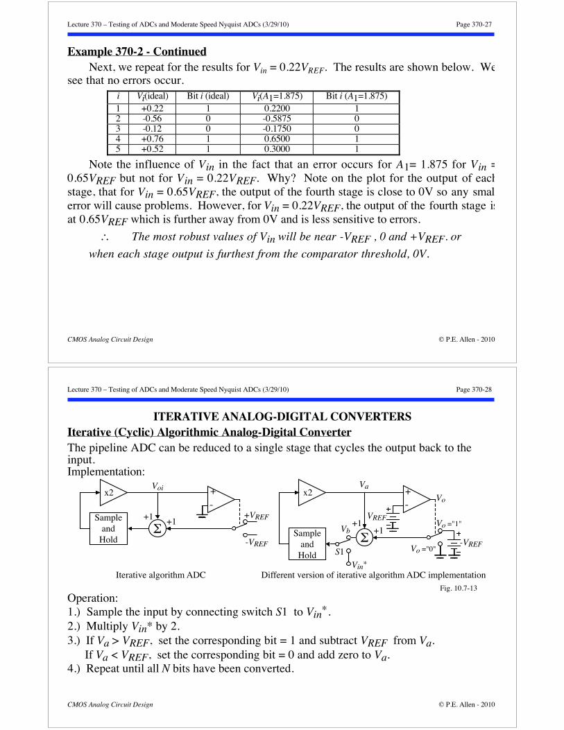
Example 370-2 - ContinuedNext, we repeat for the results for Vin = 0.22VREF. The results are shown below. We
see that no errors occur.i Vi(ideal) Bit i (ideal) Vi(A1=1.875) Bit i (A1=1.875)1 +0.22 1 0.2200 12 -0.56 0 -0.5875 03 -0.12 0 -0.1750 04 +0.76 1 0.6500 15 +0.52 1 0.3000 1
Note the influence of Vin in the fact that an error occurs for A1= 1.875 for Vin =0.65VREF but not for Vin = 0.22VREF. Why? Note on the plot for the output of eachstage, that for Vin = 0.65VREF, the output of the fourth stage is close to 0V so any smallerror will cause problems. However, for Vin = 0.22VREF, the output of the fourth stage isat 0.65VREF which is further away from 0V and is less sensitive to errors.
The most robust values of Vin will be near -VREF , 0 and +VREF. or
when each stage output is furthest from the comparator threshold, 0V.
Lecture 370 – Testing of ADCs and Moderate Speed Nyquist ADCs (3/29/10) Page 370-28
CMOS Analog Circuit Design © P.E. Allen - 2010
ITERATIVE ANALOG-DIGITAL CONVERTERSIterative (Cyclic) Algorithmic Analog-Digital ConverterThe pipeline ADC can be reduced to a single stage that cycles the output back to theinput.Implementation:
+-
ΣSample
andHold
x2
+VREF
-VREF
Voi
+1 +1
+-
ΣSampleand
Hold
x2
VREF
Va
+1+1
S1
Vb
Vo
Vin*
-VREF
Vo ="1"
Vo ="0"
Iterative algorithm ADC Different version of iterative algorithm ADC implementationFig. 10.7-13
Operation:1.) Sample the input by connecting switch S1 to Vin*.2.) Multiply Vin* by 2.3.) If Va > VREF, set the corresponding bit = 1 and subtract VREF from Va. If Va < VREF, set the corresponding bit = 0 and add zero to Va.4.) Repeat until all N bits have been converted.

Lecture 370 – Testing of ADCs and Moderate Speed Nyquist ADCs (3/29/10) Page 370-29
CMOS Analog Circuit Design © P.E. Allen - 2010
Example 370-3 - Conversion Process of an Iterative, Algorithmic Analog-DigitalConverter
The iterative, algorithmic analog-digital converter is to be used to convert an analogsignal of 0.8VREF. The figure below shows the waveforms for Va and Vb during theprocess. T is the time for one iteration cycle.1.) The analog input of 0.8VREF givesVa = 1.6VREF and Vb = 0.6VREF and the MSB as 1.2.) Vb is multiplied by two to give Va = 1.2VREF. The next bit is also 1 and Vb = 0.2VREF.3.) The third iteration givesVa = 0.4VREF, making the next bit is 0 and Vb = 0.4VREF .
4.) The fourth iteration gives Va = 0.8VREF, giving Vb = 0.8VREF and the fourth bit as 0.5.) The fifth iteration gives Va = 1.6VREF, Vb = 0.6VREF and the fifth bit as 1.The digital word after the fifth iteration is 11001 and is equivalent to an analog voltage of0.78125VREF.
������������
0.0
0.4
0.8
1.2
1.6
2.0
0 1 2 3 4 5t/T
Va/VREF
0.0
0.4
0.8
1.2
1.6
2.0
0 1 2 3 4 5t/T
Vb/VREF
������������
Fig. 10.7-14.
Lecture 370 – Testing of ADCs and Moderate Speed Nyquist ADCs (3/29/10) Page 370-30
CMOS Analog Circuit Design © P.E. Allen - 2010
SELF-CALIBRATION TECHNIQUESSelf-Calibrating Analog-Digital ConvertersSelf-calibration architecture for a m-bit charge scaling, k-bit voltage scaling successiveapproximation ADC
Comments:• Self-calibration can be
accomplished during acalibration cycle or at start-up
• In the above scheme, the LSB bits are not calibrated• Calibration can extend the resolution to 2-4 bits more that without calibration
+-
C1
VREF
C2 C3 Cm-1
Successive Approximation
Register
Cm
k-bits
m+k-bits
Cm
m-bit subDAC
k-bitsubDAC
m+2-bitCalibration
DAC
S1
ControlLogic
Register
Adder
Data Register
Vε1 Vε2
To SuccessiveApproximationRegister
Data Output
m control lines
Fig.10.7-15

Lecture 370 – Testing of ADCs and Moderate Speed Nyquist ADCs (3/29/10) Page 370-31
CMOS Analog Circuit Design © P.E. Allen - 2010
Self-Calibrating Analog-Digital Converters - ContinuedSelf-calibration procedure starting with the MSB bit:1.) Connect C1 to VREF and theremaining capacitors (C2+C3+···+Cm+Cm = C1 ) to ground and close SF.
2.) Next, connect C1 to ground andC1 to VREF.
3.) The result will be Vx1 = C1 -C1
C1 + C1 VREF. If C1 = C1 , then Vx1 = 0.
4.) If Vx1 0, then the comparator output will be either high or low. Depending on thecomparator output, the calibration circuitry makes a correction through the calibrationDAC until the comparator output changes. At this point the MSB is calibrated and theMSB correction voltage, V 1 is stored.
5.) Proceed to the next MSB with C1 out of the array and repeat for C2 and C2 . Storethe correction voltage, V 2, in the data register.6.) Repeat for C3 with C1 and C2 out of the array. Continue until all of the capacitors ofthe MSB DAC have been corrected.Note: For normal operation, the circuit adds the correct combined correction voltage.
C1
VREF C1
C1
VREF
C1
Vx1
Fig.10.7-16
+-
+-
VREF
Connection of C1 to VREF. Connection of C1 to VREF.
Lecture 370 – Testing of ADCs and Moderate Speed Nyquist ADCs (3/29/10) Page 370-32
CMOS Analog Circuit Design © P.E. Allen - 2010
SUMMARY• Tests for the ADC include:
- Input-output test- Spectral test- FFT test- Histogram test
• Moderate Speed ADCs:Type of ADC Advantage Disadvantage
Serial ADC High resolution SlowVoltage-scaling, charge-scalingsuccessive approximation ADC
High resolution Requiresconsiderable digitalcontrol circuitry
Successive approximationusing a serial DAC
Simple Slow
Pipeline ADC Fast after initiallatency of NT
Accuracy dependson input
Iterative algorithmic ADC Simple Requires otherdigital circuitry
• Successive approximation ADCs also can be calibrated extending their resolution 2-4bits more than without calibration.