Lect14 Combo
12
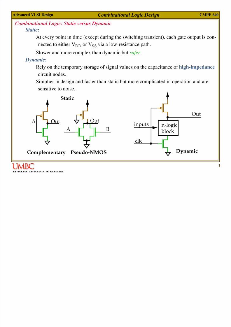
1 Advanced VLSI Design CMPE 640 Combinational Logic Design Combinational Logic: Static versus Dynamic Static: At every point in time (except during the switching transient), each gate output is con- nected to either V DD or V SS via a low-resistance path. Slower and more complex than dynamic but safer . Dynamic: Rely on the temporary storage of signal values on the capacitance of high-impedance circuit nodes. Simplier in design and faster than static but more complicated in operation and are sensitive to noise. A Out Out A Static Out n-logic block clk inputs B Dynamic Pseudo-NMOS Complementary
-
Upload
orengeneral -
Category
Documents
-
view
227 -
download
0
Transcript of Lect14 Combo
8/10/2019 Lect14 Combo
http://slidepdf.com/reader/full/lect14-combo 1/12
1
Advanced VLSI Design CMPE 640Combinational Logic Design
Combinational Logic: Static versus Dynamic
Static:At every point in time (except during the switching transient), each gate output is con-
nected to either VDD or VSS via a low-resistance path.
Slower and more complex than dynamic but safer .
Dynamic:Rely on the temporary storage of signal values on the capacitance of high-impedance
circuit nodes.
Simplier in design and faster than static but more complicated in operation and are
sensitive to noise.
A OutOut
A
Static
Out
n-logic block
clk
inputsB
DynamicPseudo-NMOSComplementary
8/10/2019 Lect14 Combo
http://slidepdf.com/reader/full/lect14-combo 2/12
2
Advanced VLSI Design CMPE 640Combinational Logic Design
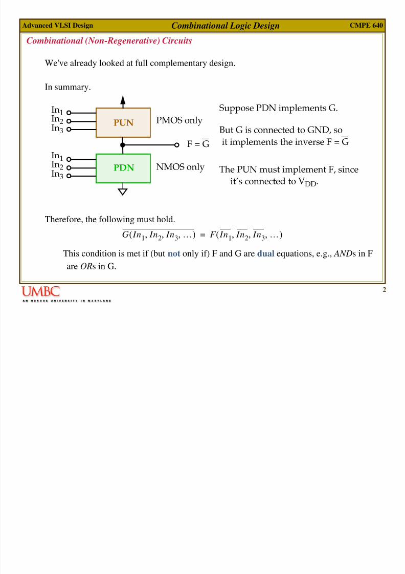
Combinational (Non-Regenerative) Circuits
We've already looked at full complementary design.
In summary.
Therefore, the following must hold.
This condition is met if (but not only if) F and G are dual equations, e.g., ANDs in F
are ORs in G.
PUN
PDN
In1In2In3
In1
In2In3
F = G
PMOS only
NMOS only
Suppose PDN implements G.
But G is connected to GND, so
it implements the inverse F = G
The PUN must implement F, since
it’s connected to VDD.
G In1 In2 In3 …, , ,( ) F In1 In2 In3 …, , ,( )=
8/10/2019 Lect14 Combo
http://slidepdf.com/reader/full/lect14-combo 3/12
3
Advanced VLSI Design CMPE 640Combinational Logic Design
Complementary CMOS Gates
Static CMOS gates inherit the nice properties of the basic CMOS inverter .
High noise margins.
No static power consumption.
Comparable rise and fall times (under the appropriate scaling conditions).
The last point needs further clarification:
This is true if the PUN and PDN networks have identical current-driving capabilities.
For the inverter, this required that p-transistors be widened .
This is complicated for complex gates since the current driving capabilities are deter-
mined by the values of the input signals as well.
As we've done in the lab, characterize based on the worst case.
8/10/2019 Lect14 Combo
http://slidepdf.com/reader/full/lect14-combo 4/12
4
Advanced VLSI Design CMPE 640Combinational Logic Design
Complementary CMOS Gates
Performing a manual analysis of the dynamic behavior of complex gates is only tractable
via a switch model.
Here, the transistor is modeled as a switch with an infinite off-resistance and a finite on
resistance, Ron.
Ron is chosen so that the equivalent RC-circuit has a propagation delay identical to the orig-
inal transistor-capacitor model.
Ron is inversely proportional to the W/L ratio but varies during the switching transient.
Deriving propagation delay can be done by analyzing the RC network.
8/10/2019 Lect14 Combo
http://slidepdf.com/reader/full/lect14-combo 5/12
5
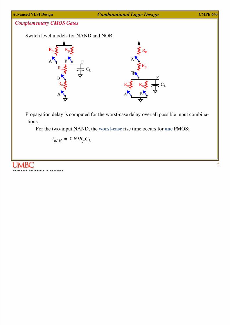
Advanced VLSI Design CMPE 640Combinational Logic Design
Complementary CMOS Gates
Switch level models for NAND and NOR:
Propagation delay is computed for the worst-case delay over all possible input combina-
tions.For the two-input NAND, the worst-case rise time occurs for one PMOS:
Rn CL
Rn
A
B
A B FRp
CLRn
A B
F
Rp Rp
A
B
Rp
Rn
t pLH 0.69 R pC L=
8/10/2019 Lect14 Combo
http://slidepdf.com/reader/full/lect14-combo 6/12
6
Advanced VLSI Design CMPE 640Combinational Logic Design
Complementary CMOS Gates
However, the worst-case (only) fall time occurs for two series NMOS:
This suggests the a 2-to-1 width scaling factor of NMOS to PMOS.
Series PMOS transistors in the pull-up path for NOR yeilds a larger difference in rise/fall
output times.
More complex network analysis:
t pHL 2 0.69× RnC L=
A
OutB
C
D
612
12
6
A
B CD 1
2
2 2
Assumes PMOS
1 is a unit-sizedtransistor.
is triple theresistance of NMOS
8/10/2019 Lect14 Combo
http://slidepdf.com/reader/full/lect14-combo 7/12
7
Advanced VLSI Design CMPE 640Combinational Logic Design
Complementary CMOS Gates
This analysis indicates the deficiencies of implementing gates with large fan-in values:
A gate with N inputs requires 2N transistors.
Other circuit styles require at most N+1 transistors, which can be a substantial advan-
tage in area, e.g., 8 versus 5 for a 4-input gate.
The propagation delay of a complementary gate deteriorates rapidly as a function of
fan-in.
First, the larger number of transistors increases the overall capacitance of the gate.
Second, the series connection in the PUN and PDN slows the gate.Widening does not improve the performance as much as predicted, since widening
increases gate and diffusion capacitance.
Fan-out in complementary gates has a larger impact on gate delay than in other circuitstyles.
Downstream gate capacitance is always two per fan-out in contrast to one in other
styles.
8/10/2019 Lect14 Combo
http://slidepdf.com/reader/full/lect14-combo 8/12
8
Advanced VLSI Design CMPE 640Combinational Logic Design
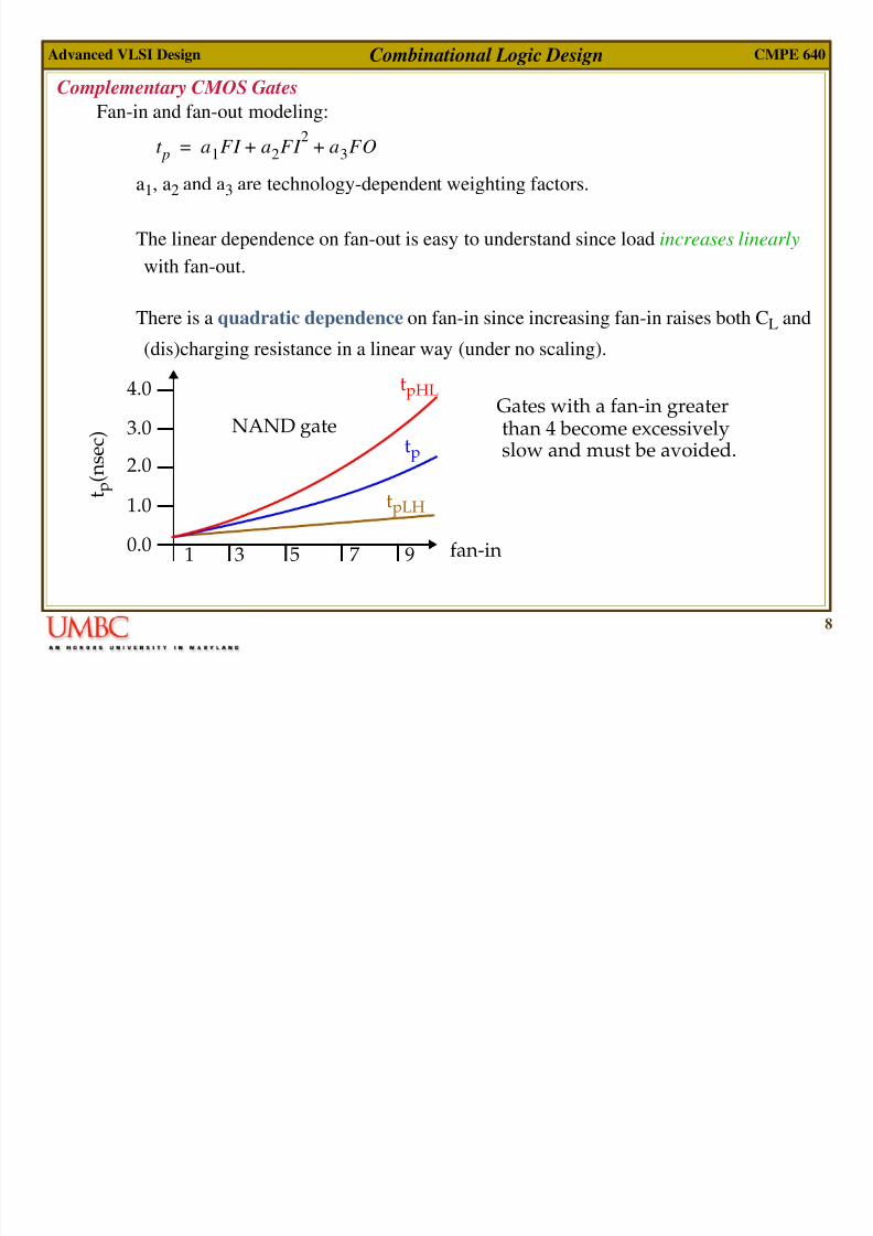
Complementary CMOS Gates
Fan-in and fan-out modeling:
a1, a2 and a3 are technology-dependent weighting factors.
The linear dependence on fan-out is easy to understand since load increases linearly with fan-out.
There is a quadratic dependence on fan-in since increasing fan-in raises both CL and
(dis)charging resistance in a linear way (under no scaling).
t p a1FI a2FI 2
a3FO+ +=
1 3 5 7 90.0
1.0
2.0
3.0
4.0
t p
( n
s e c )
fan-in
tpLH
tp
tpHL
NAND gateGates with a fan-in greaterthan 4 become excessivelyslow and must be avoided.
8/10/2019 Lect14 Combo
http://slidepdf.com/reader/full/lect14-combo 9/12
9
Advanced VLSI Design CMPE 640Combinational Logic Design
Complementary CMOS Gates
Several approaches may be used to alleviate this problem: Transistor sizing
Increasing size decreases the second-order factor in the tp expression.
However, as indicated above, if load is dominated by intrinsic capacitance (self-load-
ing), propagation delay is not improved.
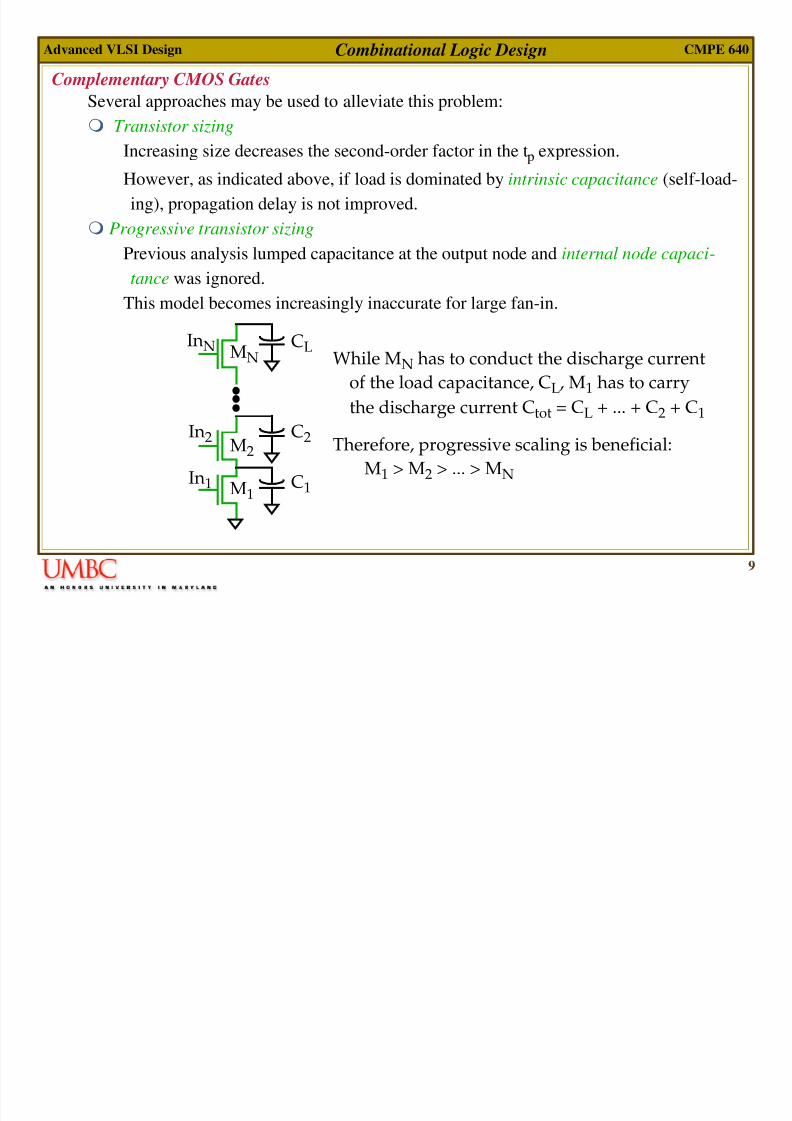
Progressive transistor sizing
Previous analysis lumped capacitance at the output node and internal node capaci-
tance was ignored.
This model becomes increasingly inaccurate for large fan-in.
In1 M1
M1 > M2 > ... > MN
In2
C1
M2
MNInN
C2
CLWhile MN has to conduct the discharge current
of the load capacitance, CL, M1 has to carry
the discharge current Ctot = CL + ... + C2 + C1
Therefore, progressive scaling is beneficial:
8/10/2019 Lect14 Combo
http://slidepdf.com/reader/full/lect14-combo 10/12
10
Advanced VLSI Design CMPE 640Combinational Logic Design
Complementary CMOS Gates
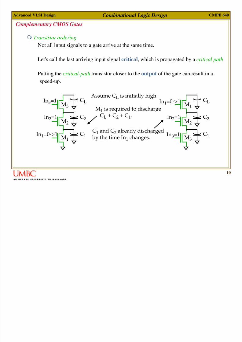
Transistor ordering
Not all input signals to a gate arrive at the same time.
Let's call the last arriving input signal critical, which is propagated by a critical path.
Putting the critical-path transistor closer to the output of the gate can result in a
speed-up.
In1=0->1M1
In2=1
C1
M2
M3In3=1
C2
CL Assume CL is initially high.
M1 is required to dischargeCL + C2 + C1.
M3
In2=1
C1
M2
M1
C2
CL
C1 and C2 already discharged
In1=0->1
In3=1 by the time In1 changes.
8/10/2019 Lect14 Combo
http://slidepdf.com/reader/full/lect14-combo 11/12
11
Advanced VLSI Design CMPE 640Combinational Logic Design
Complementary CMOS Gates
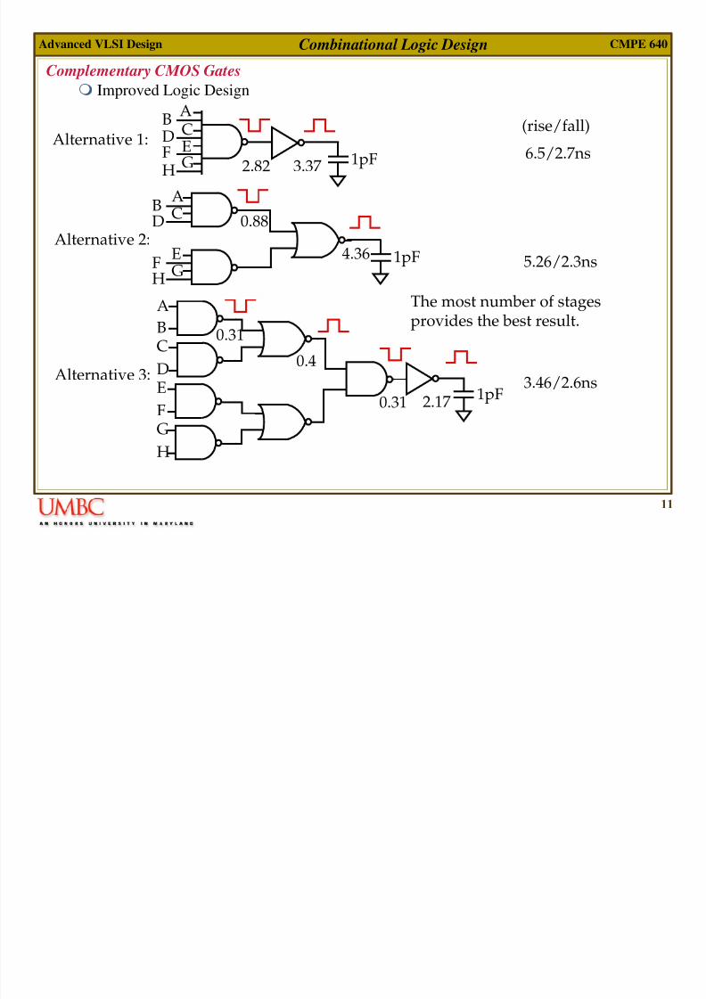
Improved Logic Design
Alternative 1:1pF
(rise/fall)
6.5/2.7ns
ABDFH
CEG
AB CD
EF G
H
1pF 5.26/2.3ns
Alternative 2:
A
BC
DAlternative 3: E
FG
H
1pF 3.46/2.6ns
The most number of stagesprovides the best result.
2.82 3.37
0.88
4.36
0.4
0.31
0.31 2.17
8/10/2019 Lect14 Combo
http://slidepdf.com/reader/full/lect14-combo 12/12
12
Advanced VLSI Design CMPE 640Combinational Logic Design
Complementary CMOS Gates
Use Another Circuit Style
Ratioed
Pass-transitor logic
Plus others to be discussed
These techniques deal with improving performance of gates with large fan-ins.
Often speed is dominated by the fan-out factor.
Scaling the transistors up in complex logic gates to drive large loads is expensive in terms
of area.
Instead, a buffer (an inverter, or sequence of inverters) can be inserted between the complex
gate and the fan-out.
Scaling is applied to the buffer transistors -- the complex gate uses minimum size transis-
tors.