Leakage Power Reduction in 5-Bit Full Adder using Keeper ....pdf · calculate power consumption of...
5
International Journal of Science and Research (IJSR) ISSN (Online): 2319-7064 Impact Factor (2012): 3.358 Volume 3 Issue 8, August 2014 www.ijsr.net Licensed Under Creative Commons Attribution CC BY Leakage Power Reduction in 5-Bit Full Adder using Keeper & Footer Transistor Narendra Yadav 1 , Vipin Kumar Gupta 2 1 Department of Electronics and Communication, Gyan Vihar University, Jaipur, Rajasthan, India 2 Assistant Professor, Department of Electronics and Communication, Gyan Vihar University, Jaipur, Rajasthan, India Abstract: In the present scenario Power consumption plays an imperative role specifically in the field of VLSI. Every designer, either an analog circuit or a digital circuit designer is concerned about the amount of the power a circuit is going to consume in the end. The main objective of this project is to design and implement of the leakage power reduction in 5-bit Full Adder (Domino Logic and Transmission Gate) technology using of footer and Keeper transistor. Keeper and Footer transistor using Transmission gate or Domino Logic are used to cooperate in reduction static power dissipation in 5-Bit Full Adder. There is reduction of 72.18% in power consumption by 5-bit transmission gate full adder with footer transistor as compared to 5-bit full adder on Tanner Tools. Keywords: Domino Logic Style, Keeper transistor, Footer transistor, Transmission Gate, Feedback 1. Introduction ADDITION is one of the fundamental arithmetic operations. It is used extensively in many VLSI systems such as application-specific DSP architectures and microprocessors. In addition to its main task, which is adding binary numbers, it is the nucleus of many other useful operations such as subtraction, Multiplication, division, addresses calculation etc. The adder is one of the most vital circuitry of a processor, as it is extensively used in the Arithmetic Logic Unit (ALU), in the floating-point unit and for address generation in case of cache or memory. Power efficient VLSI circuits are increasing day by day as rising demand of smart phones & Laptops. Extensive variants of full adders have been investigated by the academic and industrial research communities. The usual performance evaluations are speed, power consumption, and area. The demand of Adder is continuously increasing as the fields like microprocessors and digital signal processing chips. This paper deals reduction in power reduction with various adders implemented using CMOS logic style. The choice of logic style to design digital circuits strongly influences the circuit performance. The delay time depends on the size of transistors, the number of transistors per stack, the parasitic capacitance including intrinsic capacitance and capacitance due to intracellular and intercellular routing, and the logic depth (i.e., number of logic gates in the critical path). The dynamic power consumption depends on the switching activity and the number and size of transistors [1]. Among other things, the die area depends on the number and size of transistors and routing complexity. Power consumption is an important factor in CMOS circuit. The advantage of CMOS circuit is that it dissipates/consumes less power than logic families with resistive loads. Due to this reason it is widely used in manufactured integrated circuit. While during designing chips the power consumption of CMOS devices are not the major factor. Speed and area are the design parameters, which are the factor of designing chips. To reduce power consumption, various techniques are used such that domino logic, keeper, footer transistor and transmission gate that are described in section III. 2. Conventional Full Adder A Full Adder is a combinational circuit that has three single binary digits inputs A, B and Cin and has two outputs sum(S) and carry out (Cout) that are obtained by the addition of three single-bit input signals A, B and Cin. A and B are the operands, and Cin is a bit carried in from the next less significant stage (LSB). Boolean Expression: SUM=A x or B x or Cin CARRY=A.B + B Cin + A Cin =A.B + Cin (A + B) Figure 1: Gate Schematic for Conventional Full Adder Table 1: Truth Table of Full Adder A B C in SUM Cout 0 0 0 0 0 0 0 1 1 0 0 1 0 1 0 0 1 1 0 1 1 0 0 1 0 1 0 1 0 1 1 1 0 0 1 1 1 1 1 1 Paper ID: 02015572 1100
Transcript of Leakage Power Reduction in 5-Bit Full Adder using Keeper ....pdf · calculate power consumption of...
International Journal of Science and Research (IJSR) ISSN (Online): 2319-7064
Impact Factor (2012): 3.358
Volume 3 Issue 8, August 2014 www.ijsr.net
Licensed Under Creative Commons Attribution CC BY
Leakage Power Reduction in 5-Bit Full Adder using Keeper & Footer Transistor
Narendra Yadav1, Vipin Kumar Gupta2
1Department of Electronics and Communication, Gyan Vihar University, Jaipur, Rajasthan, India
2Assistant Professor, Department of Electronics and Communication, Gyan Vihar University, Jaipur, Rajasthan, India
Abstract: In the present scenario Power consumption plays an imperative role specifically in the field of VLSI. Every designer, either an analog circuit or a digital circuit designer is concerned about the amount of the power a circuit is going to consume in the end. The main objective of this project is to design and implement of the leakage power reduction in 5-bit Full Adder (Domino Logic and Transmission Gate) technology using of footer and Keeper transistor. Keeper and Footer transistor using Transmission gate or Domino Logic are used to cooperate in reduction static power dissipation in 5-Bit Full Adder. There is reduction of 72.18% in power consumption by 5-bit transmission gate full adder with footer transistor as compared to 5-bit full adder on Tanner Tools. Keywords: Domino Logic Style, Keeper transistor, Footer transistor, Transmission Gate, Feedback 1. Introduction ADDITION is one of the fundamental arithmetic operations. It is used extensively in many VLSI systems such as application-specific DSP architectures and microprocessors. In addition to its main task, which is adding binary numbers, it is the nucleus of many other useful operations such as subtraction, Multiplication, division, addresses calculation etc. The adder is one of the most vital circuitry of a processor, as it is extensively used in the Arithmetic Logic Unit (ALU), in the floating-point unit and for address generation in case of cache or memory. Power efficient VLSI circuits are increasing day by day as rising demand of smart phones & Laptops. Extensive variants of full adders have been investigated by the academic and industrial research communities. The usual performance evaluations are speed, power consumption, and area. The demand of Adder is continuously increasing as the fields like microprocessors and digital signal processing chips. This paper deals reduction in power reduction with various adders implemented using CMOS logic style. The choice of logic style to design digital circuits strongly influences the circuit performance. The delay time depends on the size of transistors, the number of transistors per stack, the parasitic capacitance including intrinsic capacitance and capacitance due to intracellular and intercellular routing, and the logic depth (i.e., number of logic gates in the critical path). The dynamic power consumption depends on the switching activity and the number and size of transistors [1]. Among other things, the die area depends on the number and size of transistors and routing complexity. Power consumption is an important factor in CMOS circuit. The advantage of CMOS circuit is that it dissipates/consumes less power than logic families with resistive loads. Due to this reason it is widely used in manufactured integrated circuit. While during designing chips the power consumption of CMOS devices are not the major factor. Speed and area are the design parameters, which are the factor of designing chips.
To reduce power consumption, various techniques are used such that domino logic, keeper, footer transistor and transmission gate that are described in section III. 2. Conventional Full Adder A Full Adder is a combinational circuit that has three single binary digits inputs A, B and Cin and has two outputs sum(S) and carry out (Cout) that are obtained by the addition of three single-bit input signals A, B and Cin. A and B are the operands, and Cin is a bit carried in from the next less significant stage (LSB). Boolean Expression: SUM=A x or B x or Cin CARRY=A.B + B Cin + A Cin =A.B + Cin (A + B)
Figure 1: Gate Schematic for Conventional Full Adder
Table 1: Truth Table of Full Adder
A B C in SUM Cout 0 0 0 0 0 0 0 1 1 0 0 1 0 1 0 0 1 1 0 1 1 0 0 1 0 1 0 1 0 1 1 1 0 0 1 1 1 1 1 1
Paper ID: 02015572 1100
International Journal of Science and Research (IJSR) ISSN (Online): 2319-7064
Impact Factor (2012): 3.358
Volume 3 Issue 8, August 2014 www.ijsr.net
Licensed Under Creative Commons Attribution CC BY
Figure 2: The Conventional CMOS Full Adder
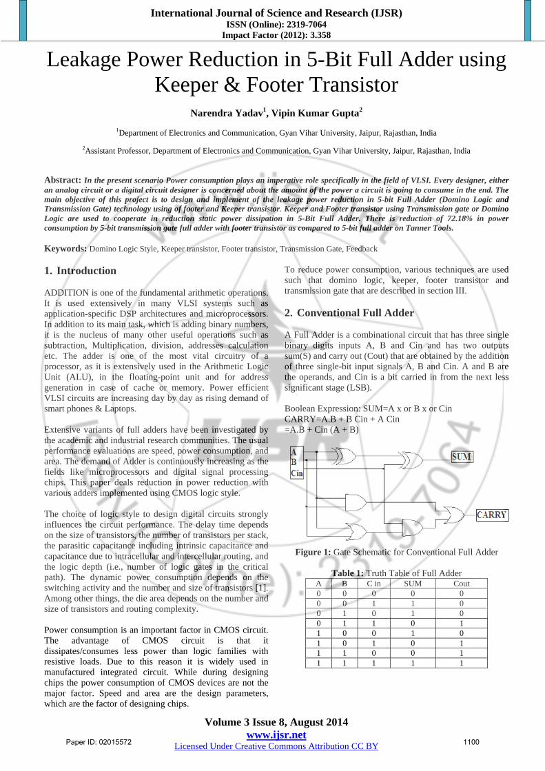
The CMOS full adder [7] has 28 transistors and is based on the regular CMOS structure is shown in figure2. 3. Methods for Reduce Power 3.1 Domino Logic Domino logic is a CMOS-based formation of the dynamic logic techniques based on either PMOS or NMOS transistors. It is also known as dynamic logic (digital electronics).It permits a rail-to-rail logic swing. It was invented for increase speed up of circuits and power consumption. The dynamic logic circuit needs two phases [4]. The first phase: when CLK is low (0), then evaluate N-FET is OFF and precharge P-FET is ON, then output node is precharged to VDD and another nodes precharge to VDD-Vth,n and depends on the value of inputs. The second phase: when CLK is high (1), then evaluate N-FET is ON and precharge P-FET is OFF, then output node is discharged depending on the value of inputs if configuration of inputs are conducting path to Ground, otherwise output node keeps high charged[4].
Figure 3: Basic structure of Domino-Logic circuit
Figure 4: Waveform of the clock needed to operate domino
logic 3.2 Employing Keeper The simplest way to eliminate the power consumption problem of 5-bit full adder the always-on keeper in the evaluation phase of domain gates, is to employ a feedback weak PMOS Keeper [4,5] illustrated in figure 5:
Figure 5: Weak PMOS Keeper to compensate for the
leakage through pull-down network. 3.3 Employing Footer Another method to eliminate the power consumption problem in 5-bit full adder by connecting a NMOS footer transistor to ground [2] illustrated in figure 6:
Figure 6: Basic structure of NMOS Footer Transistor
Paper ID: 02015572 1101
International Journal of Science and Research (IJSR) ISSN (Online): 2319-7064
Impact Factor (2012): 3.358
Volume 3 Issue 8, August 2014 www.ijsr.net
Licensed Under Creative Commons Attribution CC BY
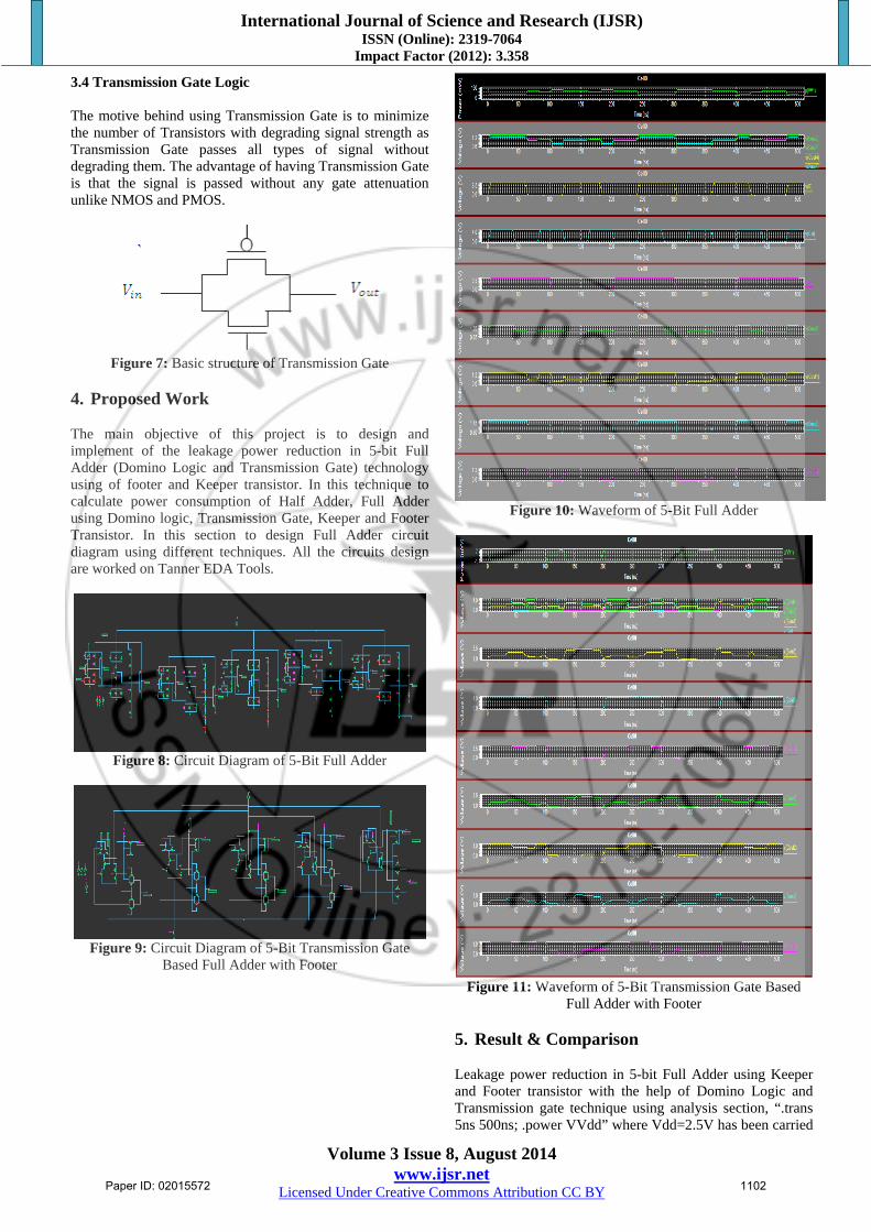
3.4 Transmission Gate Logic The motive behind using Transmission Gate is to minimize the number of Transistors with degrading signal strength as Transmission Gate passes all types of signal without degrading them. The advantage of having Transmission Gate is that the signal is passed without any gate attenuation unlike NMOS and PMOS.
Figure 7: Basic structure of Transmission Gate
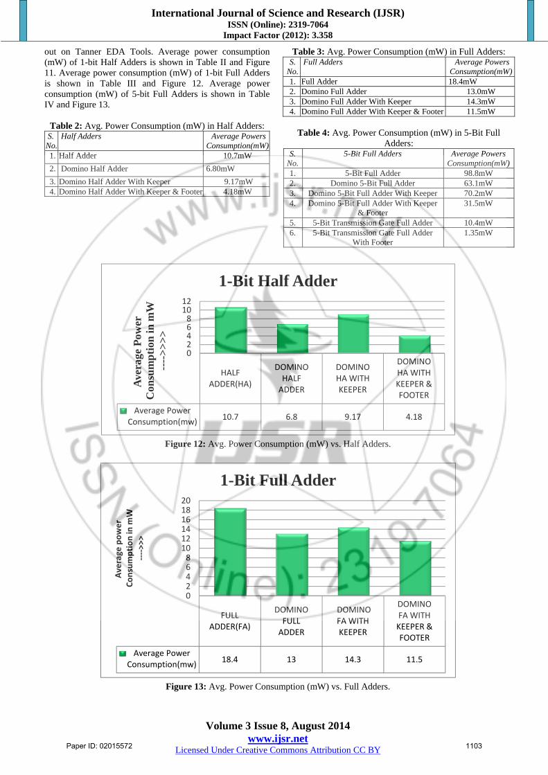
4. Proposed Work The main objective of this project is to design and implement of the leakage power reduction in 5-bit Full Adder (Domino Logic and Transmission Gate) technology using of footer and Keeper transistor. In this technique to calculate power consumption of Half Adder, Full Adder using Domino logic, Transmission Gate, Keeper and Footer Transistor. In this section to design Full Adder circuit diagram using different techniques. All the circuits design are worked on Tanner EDA Tools.
Figure 8: Circuit Diagram of 5-Bit Full Adder
Figure 9: Circuit Diagram of 5-Bit Transmission Gate
Based Full Adder with Footer
Figure 10: Waveform of 5-Bit Full Adder
Figure 11: Waveform of 5-Bit Transmission Gate Based
Full Adder with Footer 5. Result & Comparison Leakage power reduction in 5-bit Full Adder using Keeper and Footer transistor with the help of Domino Logic and Transmission gate technique using analysis section, “.trans 5ns 500ns; .power VVdd” where Vdd=2.5V has been carried
Paper ID: 02015572 1102
International Journal of Science and Research (IJSR) ISSN (Online): 2319-7064
Impact Factor (2012): 3.358
Volume 3 Issue 8, August 2014 www.ijsr.net
Licensed Under Creative Commons Attribution CC BY
out on Tanner EDA Tools. Average power consumption (mW) of 1-bit Half Adders is shown in Table II and Figure 11. Average power consumption (mW) of 1-bit Full Adders is shown in Table III and Figure 12. Average power consumption (mW) of 5-bit Full Adders is shown in Table IV and Figure 13.
Table 2: Avg. Power Consumption (mW) in Half Adders: S. No.
Half Adders Average Powers Consumption(mW)
1. Half Adder 10.7mW
2. Domino Half Adder 6.80mW
3. Domino Half Adder With Keeper 9.17mW 4. Domino Half Adder With Keeper & Footer 4.18mW
Table 3: Avg. Power Consumption (mW) in Full Adders: S.
No. Full Adders Average Powers
Consumption(mW)1. Full Adder 18.4mW 2. Domino Full Adder 13.0mW 3. Domino Full Adder With Keeper 14.3mW 4. Domino Full Adder With Keeper & Footer 11.5mW
Table 4: Avg. Power Consumption (mW) in 5-Bit Full
Adders: S.
No.5-Bit Full Adders Average Powers
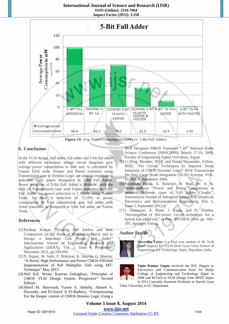
Consumption(mW)1. 5-Bit Full Adder 98.8mW 2. Domino 5-Bit Full Adder 63.1mW 3. Domino 5-Bit Full Adder With Keeper 70.2mW 4. Domino 5-Bit Full Adder With Keeper
& Footer 31.5mW
5. 5-Bit Transmission Gate Full Adder 10.4mW 6. 5-Bit Transmission Gate Full Adder
With Footer 1.35mW
HALF ADDER(HA)
DOMINO HALF ADDER
DOMINO HA WITH KEEPER
DOMINO HA WITH KEEPER & FOOTER
Average Power Consumption(mw)
10.7 6.8 9.17 4.18
024681012
Ave
rage
Pow
er
Con
sum
pti
on in
mW
----
>>
>>
1-Bit Half Adder
Figure 12: Avg. Power Consumption (mW) vs. Half Adders.
FULL ADDER(FA)
DOMINO FULL ADDER
DOMINO FA WITH KEEPER
DOMINO FA WITH KEEPER & FOOTER
Average Power Consumption(mw)
18.4 13 14.3 11.5
02468101214161820
Average
power
Consumption in
mW
‐‐‐‐>>>
1-Bit Full Adder
Figure 13: Avg. Power Consumption (mW) vs. Full Adders.
Paper ID: 02015572 1103
International Journal of Science and Research (IJSR) ISSN (Online): 2319-7064
Impact Factor (2012): 3.358
Volume 3 Issue 8, August 2014 www.ijsr.net
Licensed Under Creative Commons Attribution CC BY
Figure 14: Avg. Power Consumption (mW) vs. 5-Bit Full Adders.
6. Conclusion In the VLSI design, half adder, full adder and 5-bit full adder with different techniques design circuit diagrams give average power consumption in mW unit, is calculated by Tanner EDA tools. Keeper and Footer transistor using Transmission gate or Domino Logic are used to cooperate in reduction static power dissipation in 5-Bit Full Adder. Power reduction of 5-Bit Full Adder is 98.8mW; with the help of Transmission Gate with Footer transistor in 5-Bit Full Adder has power reduction is 1.35mW using Tanner Tools. So there is reduction of 72.18% in power consumption by 5-bit transmission gate full adder with footer transistor as compared to 5-bit full adder on Tanner Tools. References
[1] Pardeep Kumar, “Existing Full Adders and their
Comparison on the Basis of Simulation Result and to Design a Improved Low Power Full Adder” International Journal of Engineering Research and Applications (IJERA), Vol. 2, Issue 6, November- December 2012, pp.599-606.
[2] N. Rajput, M. Sethi, P. Dobriyal, K. Sharma, G. Sharma, “A Novel, High Performance and Power CMOS Efficient Implementation of 8x8 Multiplier Unit using MT- Technique” May 2013.
[3] Neil H.E. Weste, Kamran Eshraghian, “Principles of CMOS VLSI Design System Perspective” Second Edition.
[4] Sherif M. Sharroush, Yasser S. Abdalla, Ahmed A. Dessouki, and EI-Sayed A EI-Badawy, “Compensating For the Keeper current of CMOS Domino Logic Using a
Well Designed NMOS Transistor.” 26th National Radio Science Conference (NRSC2009), March 17-19, 2009, Faculty of Engineering Future University, Egypt.
[5] Li Ding, Member, IEEE, and Pinaki Mazumder, Fellow, IEEE, “On Circuit Techniques to Improve Noise Immunity of CMOS Dynamic Logic” IEEE Transactions On Very Large Scale Integration (VLSI) Systems, VOL. 12, NO. 9, September 2004.
[6] Saradindu Panda, A. Banerjee, B. Maji, Dr. A. K. Mukhopadhyay “Power and Delay Comparison in between Different types of Full Adder Circuits”, International Journal of Advanced Research in Electrical, Electronics and Instrumentation Engineering, Vol. 1, Issue 3, September 2012.0
[7] I. Hassoune, A. Neve, J. Legat, and D. Flandre, “Investigation of low-power circuit techniques for a hybrid full-adder cell,” in Proc. PATMOS 2004, pp. 189–197, Springer-Verlag.
Author Profile
Narendra Yadav is a final year student of M. Tech (Dual Degree) EC+VLSI from Gyan Vihar School of Engineering and Technology Jaipur, Rajasthan, India.
Vipin Kumar Gupta received the B.E. Degree in Electronics and Communication from Sri Balaji College of Engineering and Technology Jaipur in 2008 and M.Tech in VLSI Design from MNIT Jaipur in 2011.Currently Assistant Professor at Suresh Gyan
Vihar University in EC Deparment.
Paper ID: 02015572 1104