Leakage Aware Design for Next Generation's...
23
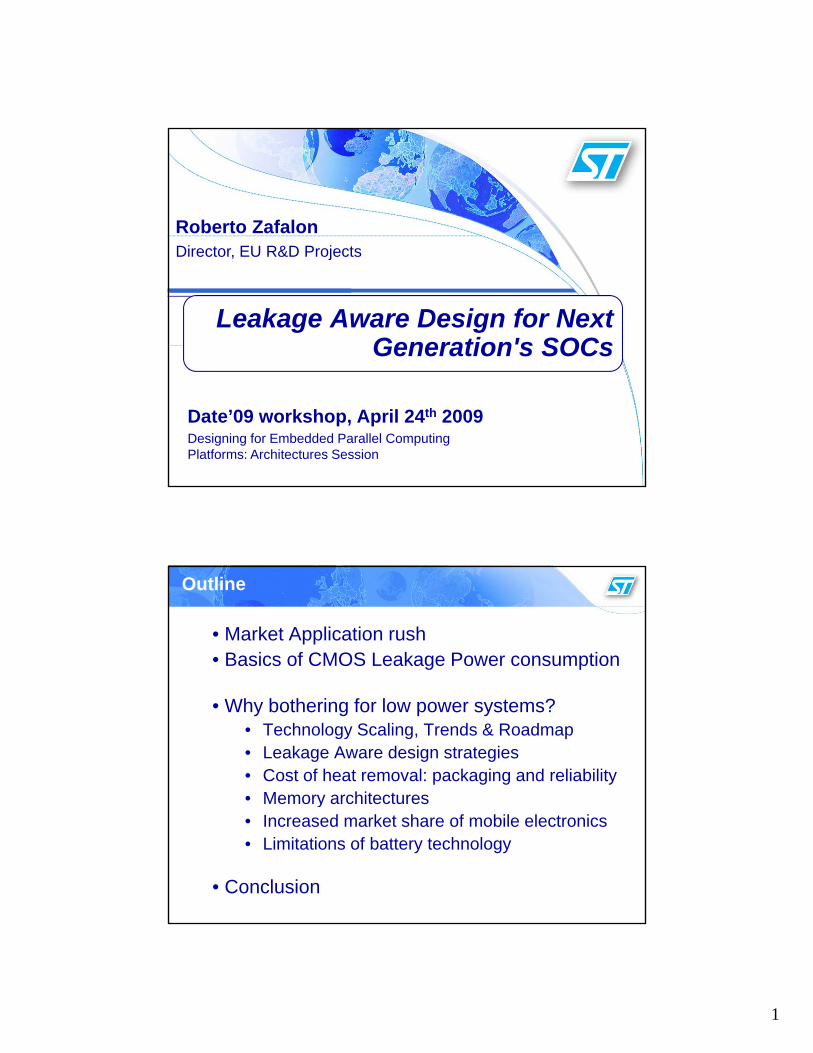
1 Roberto Zafalon Di t EU R&D P j t Leakage Aware Design for Next Generation's SOCs Director, EU R&D Projects Roberto Zafalon European R&D Projects Date’09 workshop, April 24 th 2009 Designing for Embedded Parallel Computing Platforms: Architectures Session Outline • Market Application rush • Basics of CMOS Leakage Power consumption • Why bothering for low power systems? • Technology Scaling, Trends & Roadmap • Leakage Aware design strategies • Cost of heat removal: packaging and reliability • Memory architectures • Increased market share of mobile electronics • Limitations of battery technology • Conclusion
-
Upload
nguyenphuc -
Category
Documents
-
view
215 -
download
0
Transcript of Leakage Aware Design for Next Generation's...
1
Roberto ZafalonDi t EU R&D P j t
Leakage Aware Design for Next Generation's SOCs
Director, EU R&D Projects
Roberto ZafalonEuropean R&D ProjectsDate’09 workshop, April 24th 2009
Designing for Embedded Parallel Computing Platforms: Architectures Session
Outline
• Market Application rush • Basics of CMOS Leakage Power consumption
• Why bothering for low power systems?• Technology Scaling, Trends & Roadmap• Leakage Aware design strategies• Cost of heat removal: packaging and reliability• Memory architecturesy• Increased market share of mobile electronics• Limitations of battery technology
• Conclusion

2
30 Years of Electronics Industry CAGRSemic. Capex:17%
Semic. Market:
ElectronicSystems:8 %
Market:15%
WW GDP: 3,4%
Market Application rush
Autonomous3D projecteddisplay
Ubiquitousnavigation
Structured decoding
3D TV 3D gaming
3D ambientinteraction
1 TOPS/W
100 GOPS/W
5 GOPS/WSign
recognitionA/V
streaming
Adaptiveroute
Collisionavoidance
drivingdisplayHMI by motion
Gesture detection
Gbit radio
UWB
Structured encoding
H264encoding
Image
dictation LanguageEmotionrecognition
Gesturerecognition
Expressionrecognition
Year of Introduction2005 2007 2009 2011 2013 2015
Si Xray802.11n
H264decoding
recognition
Fully recognition(security)
Autopersonalization
MobileBase-band

3
CMOS Roadmap: 3 main showstoppers
Pat Gelsinger, CTO Intel Corp.Quote from DAC’04 Keynote:
Power is the only limiter !!Power is the only limiter !!
CMOS Roadmap: 3 main showstoppers:
1. Subthreshold Leakage Current ( Ioff )
2 Huge Process Variation Spread2. Huge Process Variation Spread
3. Interconnect Performance and Signal Integrity
A further quote, to start with…Roberto Zafalon, Low Power System Design mngr,
STMicroelectronics
CLEAN-IP General Project Manager
Quote from CLEAN Press Release published by EETIMES on Jan 2006:
“Semiconductor industry urges to overcome the technology shortcomings for 65nm and below, and in particular, process variability and unreliability,
as well as leakage currents ”as well as leakage currents,
“Industry needs to decrease power consumption of nanoelectronic devices, increase design
productivity and thus make the raised SoC’s complexity manageable.”
4
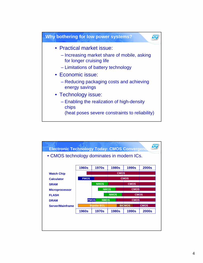
Why bothering for low power systems?
• Practical market issue:– Increasing market share of mobile, asking
for longer cruising lifefor longer cruising life– Limitations of battery technology
• Economic issue:– Reducing packaging costs and achieving
energy savings• Technology issue:
– Enabling the realization of high-density chips (heat poses severe constraints to reliability)
Electronic Technology Today: CMOS Convergence• CMOS technology dominates in modern ICs.
1960s 1970s 1980s 1990s 2000sCMOS
CMOSNMOS
CMOSPMOS
CMOSNMOS
CMOSNMOS
CMOSNMOSPMOS
Watch Chip
Calculator
SRAM
Microprocessor
FLASH
DRAMCMOSBICMOSBipolar ECL
DRAM
Server/Mainframe
1960s 1970s 1980s 1990s 2000s

5
CMOS at core of chip making still for many years
• The theoretical limit for transistor gate length on silicon is around 1.5nm.
– Today’s 65nm CMOS process has a gate length of 42nm: i.e 28X larger than the theoretical limit!
– In 32nm, the gate length is 21nm i.e. 14X above limit
• The gate delay determines the fundamental speed of the logic. The theoretical limit is 0.04ps
– Today’s 65nm logic NAND2 is ~1ps, i.e. 24X slower!• Transistor density, i.e. the number of device which can
be squeezed into a chip reaches the limit around 1 8be squeezed into a chip, reaches the limit around 1.8 billion Tx per cm².
– Today’s 65nm CMOS device is 7.5X larger! (i.e. 750Kgate/mm2 = 2.4M Tx/mm2 = 240M Tx/cm2)
• Performance as measured by clock speed, fell off Moore’s Law during the last decade, thanks to Multi Processors computing architectures.
Source: ITRS, STM, IFX
• Power consumption of a CMOS gate:P = PSW + PSC + PLk
where:• PSW = Switching (or dynamic) power.
Basics of CMOS Power Consumption
PSW Switching (or dynamic) power.• PSC = Short-circuit power.• PLk = Leakage (or stand-by) power.
• In older technologies (0.25um and above), PLk was marginal w.r.t. switching power:– Switching power minimization was the primary objective.
• In deep sub-micron processes, PLk becomes i i lcritical:
– Leakage accounts for around 5-10% of power budget at 180nm;this grows to 20-25% at 130nm and to 35-60% at 65 nm.

6
Leakage Currents in Bulk CMOS
• Isub: Subthreshold current.
• Igs, Igb, Igd: G t id t li
GATEDRAINSOURCE
IDIS
IGIgb IgdIgs
Gate oxide tunneling.
• Ijbs, Ijbd:Junction reverse current.
• IGIDL, IGISL:Gate induced D,S leakage.
• I : Impact ionization current
BULK IB
Iii
IjbdIjbs
Isub
IGIDLIGISL
• Iii: Impact ionization current.
Long Channel (L > 1 um) Very small leakage
Short Channel(L > 180nm, Tox > 30A0)Subthreshold leakage
Very Short Channel(L > 90nm, Tox > 20A0)Subthreshold +Gate leakage
Nano-scaled(L < 90nm, Tox < 20A0)Subthreshold +Gate + Junction leakage
Technology Scaling
• Smaller geometries–Higher device density:
• Smaller gate capacitance, yet many more g p , y ygates/chip
• Higher switched capacitance Higher switching power.
–Higher clock frequencies:• Higher switching power
–Lower supply voltages:• Lower switching power, but also lower speed
Lower threshold voltages Exponential leakage
• Consequence:–Power density increases as technology scales!

7
ITRS Roadmap 2007 vs Moore’s law
Squeezing costs of computing coresARM 9180 nm11.8 mm2
90 nm,
130 nm, 5.2 mm2
65 nm1.4 mm2
2.6 mm2

8
VDD (no more) scaling is increasing the «power crisis»
Evolution of VDD (LSTP)
4 55
Regular Decrease in 10 years
5V plateau
11.5
22.5
33.5
44.5
Volt
Regular Decrease in 10 years
From 5V to 1.2V (x 0.7 per node)
1.2V plateau1V plateau?1.1V
00.5
1989 1992 1995 1998 2000 2002 2004 2007 2010 2015
Year of production (ITRS)
120 90 65 32250350700 45500 180
1000Rocket
Power Trend for microprocessors• Power density in Intel’s microprocessors:
100
Wat
ts/c
m2
P4 @ 1.4GHz, 75W
10
Hot plate
PentiumPro ®
Pentium II ®
Pentium III ®
P4
Nuclear ReactorP5
Rocket Noozle
Sun’s surface
1 1.5μ 1μ 0.7μ 0.5μ 0.35μ 0.25μ 0.18μ 0.13μ 0.1μ 0.07μ 0.05μ
i386i486
Pentium ® PentiumPro ®

9
CMOS Logic Tech Overview
Source: STMicroelectronics
3000
3500
4000
[nW
]
65LP/G45GS
32LP32GP
Gate total power
1000
1500
2000
2500
Tota
l pow
er p
er g
ate
[
F=500Mhz
0
500
1% 5% 10% 20% 50% 90%
Duty Cycle [%] Source: STMicroelectronics
10
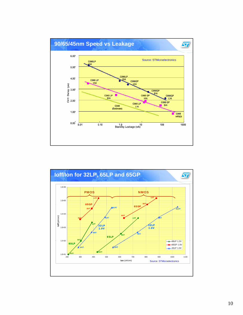
90/65/45nm Speed vs Leakage
Source: STMicroelectronics
Ioff/Ion for 32LP, 65LP and 65GP
1.E+05
1.E+06
65GP65GP
LVTLVT
SVTSVT
LVTLVT
PMOS NMOS
1 E+02
1.E+03
1.E+04
Ioff
(pA
/um
)
65LP 1 2V
65GP65GP
HVTHVT
SVTSVT
HVTHVT
65GP65GP
SVTSVT
LVTLVT
SVTSVT
LVTLVT
65LP65LP
SVTSVT
LVTLVT
32LP 32LP 1.0V1.0V
SLVTSLVT
SVTSVT
LVTLVT
32LP 32LP 1.0V1.0V
SLVTSLVT
1.E+01
1.E+02
200 300 400 500 600 700 800 900 1000 1100
Ion (uA/um)
65LP 1.2V65GP 1.0V32LP 1.0V
HVTHVT
65LP65LP
HVTHVT
HVTHVT HVTHVT
Source: STMicroelectronics

11
Technology Scaling
• Increasing contribution of leakage power:
125150
– Example: ASICs [source: STMicroelectronics]
80%
100%Itanium 2:180nm 1 5V 1 0GHz
– Example: Microprocessors [source: Intel].
0255075
100125
Power Density (Watts/cm2)
250nm 180nm 130nm 90nm 65nm
Leakage Power
Dynamic Power
0%
20%
40%
60%
80%
Itanium 2 Itanium 3
Leakage Power
I/O Power
Dynamic Power
180nm, 1.5V, 1.0GHz, 221MTx (core+cache)
Itanium 3:130nm, 1.3V, 1.5GHz, 410MTx (core+cache)
SoC Requirements for MP platforms (1)
• Processing performance is expected to grow more than 200x in the next 15 years.

12
SoC Requirements for MP platforms (2)
• # PE per chip; Processing Performance; ND2’s max switching frequency (normalized to 2007)
MOS Capacity by Dimensions
1600 0
2000.0
2400.0
k x1
000
>=0.7µ
<0.7µ >=0.4µ
<0.4µ >=0.3µ
<0.3µ >=0.2µ
0.0
400.0
800.0
1200.0
1600.0
Waf
ers/
Wee
k
<0.2µ >=0.16µ
<0.16µ >=0.12µ
<0.12µ
<0.12µ >=0.08µ
<0.08µ
Source: "Semiconductor Industry Association", Statistics Report 2008-Q2
3Q05
4Q05
1Q06
2Q06
3Q06
4Q06
1Q07
2Q07
3Q07
4Q07
1Q08
2Q08
13
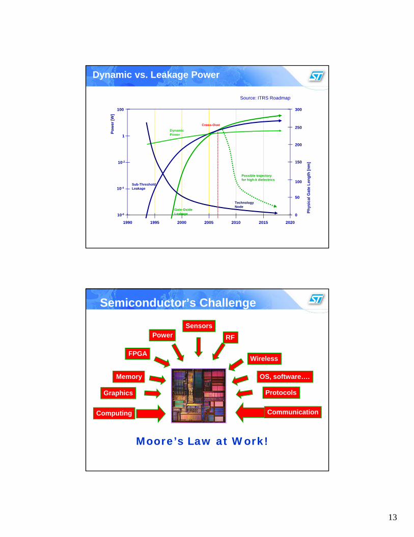
Dynamic vs. Leakage Power
100 300
250wer
[W]
Source: ITRS Roadmap
Cross-Over
10-2
10 4
1
200
150
100
250
Sub-Threshold L k
Dynamic Power
Possible trajectory for high-k dielectrics
Pow
e Le
ngth
[nm
]
1990 1995 2000 2005 2010 2015 2020
10-4
10-6
50
0Gate-Oxide Leakage
Leakage
Technology Node
Phys
ical
Gat
eSemiconductor’s Challenge
PowerSensors
RF
C i ti
Memory
FPGAWireless
OS, software….
ProtocolsGraphics
Computing Communication
Moore’s Law at Work!

14
Leakage crisis: Is it a technology issue only?
• Trends:– nominal Vdd getting stable around 1V
MOS’s Vth linearly scales to keep costant speed– MOS s Vth linearly scales to keep costant speed– But… leakage grows exponentially with Vth reduction
!!– sub-threshold current from 100 to 1000 pA/um– gate leakage to become larger that sub-threshold– total static power from 21E-12 to 60E-12 W/Transistorp
• SOI has major disadvantages w.r.t. sub-threshold reduction!
“Leakage Aware” design strategy includesA. Gate/Circuit-level techniques
Use of multiple Vth• Dual-Vth design.• Mixed-Vth (MVT) CMOS design.• MTCMOS.
Sleep transistor insertion/Voltage islands– Sleep transistor insertion/Voltage islands– State retention FFs
B. Techniques for memory circuitsCell state (stored value) determines exactly which transistors “leak” – State-preserving techniques:
• Only suitable choice for non-cache memories (e.g., scratchpad).– State-destroying techniques:y g
• Suitable for caches (can invalidate values).
C. Architectural techniques– Adaptive Body Biasing (ABB).– Adaptive Voltage Scaling (AVS).– Vth hopping.– Multiple VBB

15
0.0035 8.E-07
Static Power Dissipation (mW/Cell) HP / LSTP
Dynamic Power Consumption Per Cell -(mW/MHz) HP / LSTP
Memory Driver
DynStatic
0.0015
0.002
0.0025
0.003
3.E-07
4.E-07
5.E-07
6.E-07
7.E-07( )
0
0.0005
0.001
2005 2006 2007 2008 2009 2010 2012 2015 20180.E+00
1.E-07
2.E-07
Low Leakage Memory Approaches
• Leakage reduction techniques can be broadly classified in terms of how memory state is managed :– State-preserving techniques:
• Memory cell value is preserved when in low-leakage state.• Suitable choice for non-cache memories (e.g., scratch-pad).
– State-destroying techniques:• Memory cell value is NOT preserved when in low-leakage
state.• Suitable only for caches (can invalidate values).
• Tradeoff between:– Residual leakage paid to preserve the state.– Restoring the lost state from higher levels of the
memory hierarchy.
16
Low Leakage Memory Approaches (cont.)
• Circuit-level techniques:– Modify internal structure of SRAM cells.
• Transistor size, P/N ratio, Vth, body bias.• Additional transistors.• Precharge policy tuning
– May possibly require specialized process (e.g., different Tox, Halo doping, multiple Vth).
• Architectural techniques.Architectural techniques.– Use system level information to determine
conditions to drive portions of memory into low-leakage state.
– Portions of Memory: bit lines, blocks, regions, etc.
Spatio-Temporal-Value Cache
Tag1 Data1CM1
• Partitioned Architecure (Outcome of CLEAN):
Address
Tag DataAddress
g1 1
...
Tagi Datai
...Addressi
Sleepi
1
CMi
...
...
TagN DataNCMN
17
SoC Design Grand Challenges(source: ITRS 2007)
• MANAGEMENT OF OVERALL POWER– Due to the Moore’s law, power management is theDue to the Moore s law, power management is the
primary issue across most application segments. – Needs to be addressed across multiple levels,
especially system, design, and process technology.
• MANAGEMENT OF LEAKAGE POWER– Leakage currents increase by 10x per tech node. – From system design requirements & improvements
in CAD design tools, downto leakage and performance requirements for new architectures.
Subthreshold Leakage vs. Temperature
1,000
10,0000.10 μm
0.13 μm1,000
10,0000.10 μm
0.13 μm
10
100
1,000
Ioff
(nA
/μm
)
0.18 μm
0.25 μm
10
100
1,000
Ioff
(nA
/μm
)
0.18 μm
0.25 μm
1
30 40 50 60 70 80 90 100 110
Temp (C)
1
30 40 50 60 70 80 90 100 110
Temp (C)
18
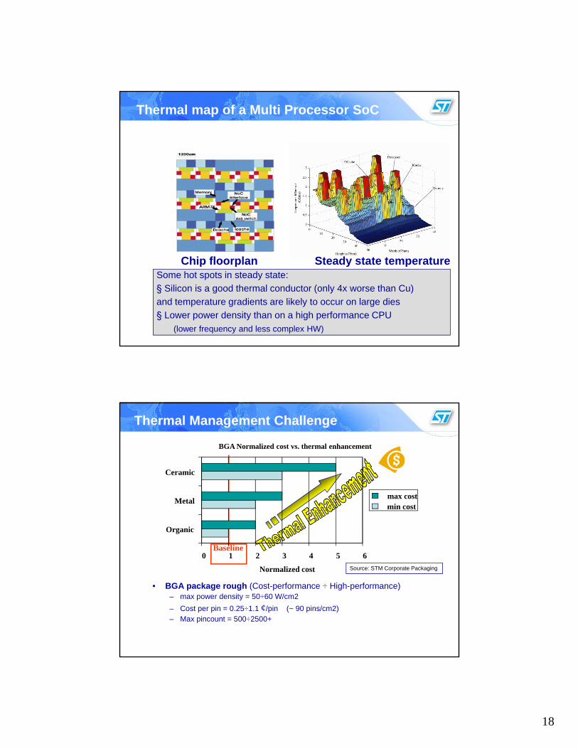
Thermal map of a Multi Processor SoC
Chip floorplan Steady state temperatureChip floorplan Steady state temperatureSome hot spots in steady state:§ Silicon is a good thermal conductor (only 4x worse than Cu) and temperature gradients are likely to occur on large dies§ Lower power density than on a high performance CPU
(lower frequency and less complex HW)
Thermal Management Challenge
BGA Normalized cost vs. thermal enhancement
Ceramic
Baseline
Source: STM Corporate Packaging
0 1 2 3 4 5 6
Organic
Metal
Normalized cost
max costmin cost
• BGA package rough (Cost-performance ÷ High-performance)– max power density = 50÷60 W/cm2– Cost per pin = 0.25÷1.1 ¢/pin (~ 90 pins/cm2)– Max pincount = 500÷2500+
19
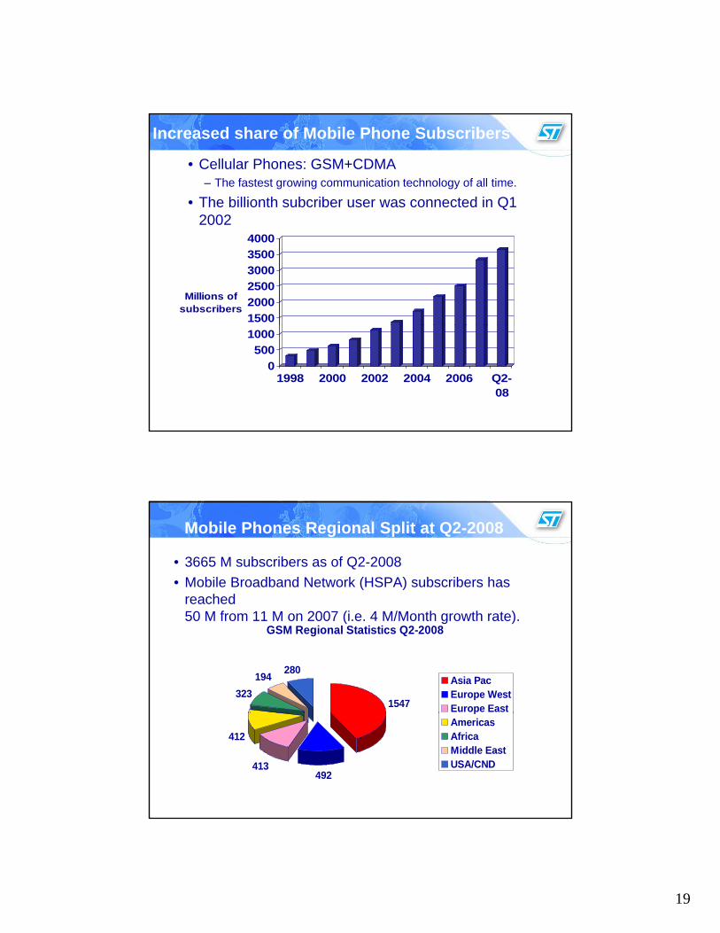
Increased share of Mobile Phone Subscribers
• Cellular Phones: GSM+CDMA– The fastest growing communication technology of all time.
• The billionth subcriber user was connected in Q1 20022002
150020002500300035004000
Millions of subscribers
0500
1000
1998 2000 2002 2004 2006 Q2-08
Mobile Phones Regional Split at Q2-2008
• 3665 M subscribers as of Q2-2008• Mobile Broadband Network (HSPA) subscribers has
reached 50 M from 11 M on 2007 (i.e. 4 M/Month growth rate).
GSM Regional Statistics Q2-2008
1547323
194 280Asia PacEurope WestEurope East
492413
412
pAmericasAfricaMiddle EastUSA/CND

20
Cellular Phone’s standby current
Nomadik™: ST’s example of Mobile Multi-Media driver
Audio Video
21
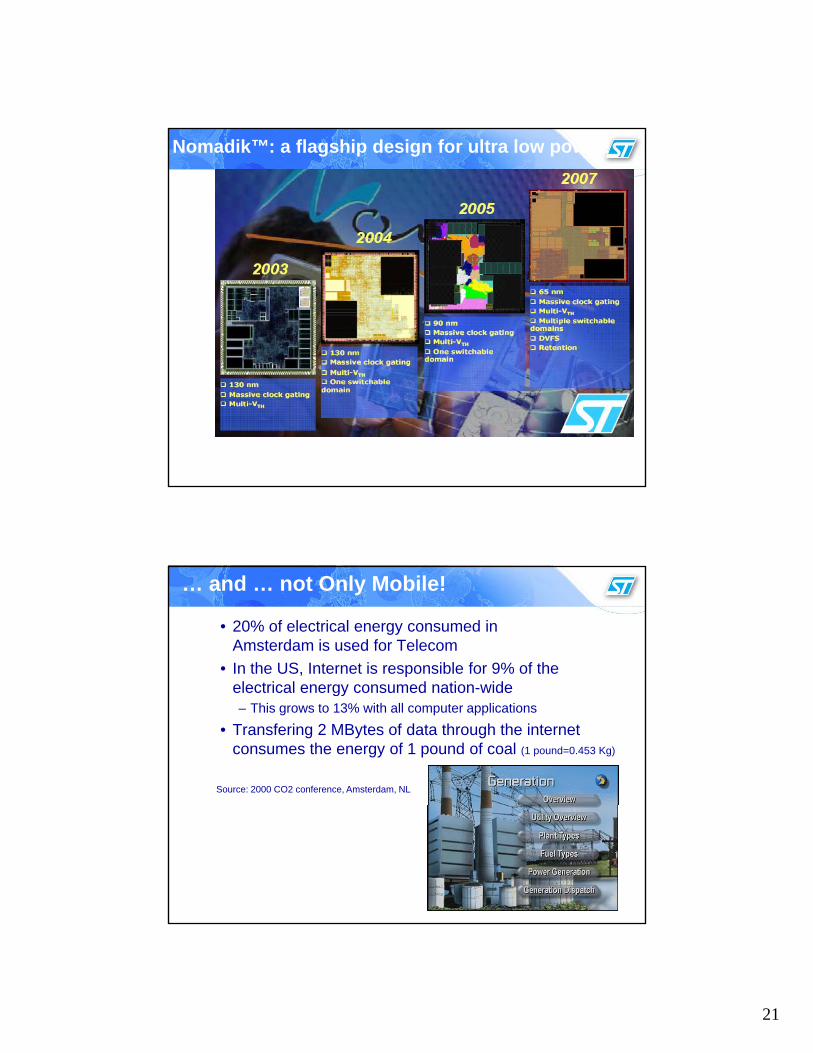
Nomadik™: a flagship design for ultra low power!
… and … not Only Mobile!
• 20% of electrical energy consumed in Amsterdam is used for Telecom
• In the US, Internet is responsible for 9% of the electrical energy consumed nation wideelectrical energy consumed nation-wide– This grows to 13% with all computer applications
• Transfering 2 MBytes of data through the internetconsumes the energy of 1 pound of coal (1 pound=0.453 Kg)
Source: 2000 CO2 conference, Amsterdam, NL

22
Complexity goes non-linear
SOXXSOXXFinanceFinance
integration
Com
plex
ity
- 5 0 %
- 4 0 %
- 3 0 %
- 2 0 %
- 10 %
0 %
10 %
2 0 %
3 0 %
4 0 %
5 0 %
3/12 12/12
LITHO & DFMLITHO & DFM
MarketsMarketsg
Cos
t
LINEARAPPROACH TO
non linear
SWSWcomplexitycomplexity IC DesignIC Design
verificationverification
Complexity
PROBLEMS!
Conclusion
• Semiconductor market is still CMOS dominated:– Switching and leakage power.
• Leakage will become dominant for technology nodes b l 65below 65nm.– Leakage power optimization must be addressed from both
technology and design points of view.
• Many circuit-level techniques have been investigated recently:– Not yet fully supported by commercial EDA tools.
• Higher-level approaches are still in their infancy:– Results are promising.
• The electronics industry calls for a REVOLUTION!

23
• Ultra low power systems• Ultra low power cognitive
Industry’s Needs
p gradio
• Energy scavenging• Micro-Nano systems• System In Package
System On Wafer…
System In Package• System On Wafer • …