
LEAD ATTACHMENT AND ENCAPSULATION TECHNIQUES FOR …
20
o (T 1 r> PH vO o o --t vO H H3 c£ H Q fe EH H P En 00 CO W w ESD-TDR-64-630 ESD RECORD COPY RETURN TO SCIENTIFIC & TECHNICAL INFORMATION DIVISION (ESTI), BUILDING 1211 W-6353 COPY NR. OF COPIES LEAD ATTACHMENT AND ENCAPSULATION TECHNIQUES FOR THIN FILM MICROCIRCUITS TECHNICAL DOCUMENTARY REPORT NO. ESD-TDR-64-630 FEBRUARY 1965 P. N. Everett -^ILPROCESgED ÜDDCTAB D PROJ OFFICE« D ACCESSION MASTER FIL* D D<VT;: Prepared for ESTI CONTJ?OL NR DIRECTORATE OF COMPUTERS cv NR ELECTRONIC SYSTEMS DIVISION AIR FORCE SYSTEMS COMMAND UNITED STATES AER FORCE L. G. Hanscom Field, Bedford, Massachusetts * J* 4493/ OF. I -CY» Project 708. 0 Prepared by THE MITRE CORPORATION Bedford, Massachusetts Contract AF 19(628)-2390 ftbOÜAlrf*'
Transcript of LEAD ATTACHMENT AND ENCAPSULATION TECHNIQUES FOR …

o (T1 r> PH vO o
o --t vO H
H3 c£ H Q fe EH
H P En 00 CO W w
ESD-TDR-64-630
ESD RECORD COPY RETURN TO
SCIENTIFIC & TECHNICAL INFORMATION DIVISION (ESTI), BUILDING 1211 W-6353
COPY NR. OF COPIES
LEAD ATTACHMENT AND ENCAPSULATION TECHNIQUES
FOR THIN FILM MICROCIRCUITS
TECHNICAL DOCUMENTARY REPORT NO. ESD-TDR-64-630
FEBRUARY 1965
P. N. Everett
-^ILPROCESgED
ÜDDCTAB D PROJ OFFICE«
D ACCESSION MASTER FIL*
D
D<VT;:
Prepared for ESTI CONTJ?OL NR
DIRECTORATE OF COMPUTERS cv NR
ELECTRONIC SYSTEMS DIVISION
AIR FORCE SYSTEMS COMMAND
UNITED STATES AER FORCE
L. G. Hanscom Field, Bedford, Massachusetts
* J* 4493/ OF. I -CY»
Project 708. 0
Prepared by
THE MITRE CORPORATION Bedford, Massachusetts
Contract AF 19(628)-2390
ftbOÜAlrf*'

Copies available at Office of Technical Services, Department of Commerce.
Qualified requesters may obtain copies from DDC. Orders will be expedited if placed through the librarian or other person designated to request documents from DOC.
When US Government drawings, specifications, or other data are used for any purpose other than a definitely related government procurement operation, the government thereby incurs no responsibility nor any obligation whatsoever; and the fact that the government may have formulated, furnished, or in any way supplied the said drawings, specifications, or other data is not to be regarded by implication or otherwise, as in any manner licensing the holder or any other person or corporation, or conveying any rights or permission to manufacture, use, or sell any patented invention that may in any way be related thereto.
Do not return this copy. Retain or destroy.

ESD-TDR-64-630 W-6353
LEAD ATTACHMENT AND ENCAPSULATION TECHNIQUES
FOR THIN FILM MICROCIRCUITS
TECHNICAL DOCUMENTARY REPORT NO. ESD-TDR-64-630
FEBRUARY 1965
P. N. Everett
Prepared for
DIRECTORATE OF COMPUTERS
ELECTRONIC SYSTEMS DIVISION
AIR FORCE SYSTEMS COMMAND
UNITED STATES AIR FORCE
L. G. Hanscom Field, Bedford, Massachusetts
Project 708. 0
Prepared by
THE MITRE CORPORATION Bedford, Massachusetts
Contract AF 19(628)-2390


ABSTRACT
The techniques described were developed for encapsulating experimental thin film circuits deposited on 0. 5-inch square glass substrates. The encapsula- tion is epoxy, with final package dimensions of 0. 6-inch square x . 125-inch thick. Up to 32 ribbon leads emerge, on . 050 centers, arranged on the periphery of the package. A factor complicating the encapsulation was the requirement that the leads emerge on the four edges of the unit. A molding process using silicone rubber molds, and a hypodermic filling arrangement was evolved.
REVIEW AND APPROVAL
This technical documentary report has been reviewed and is approved.
SEYMOUR Major, USAF Chief, Computer Division Directorate of Computers
in


SECTION I
INTRODUCTION
This report describes techniques used in lead attachment and encapsulation
for certain experimental thin film circuits being fabricated at The MITRE
Corporation.
The circuits to be encapsulated are formed on 0. 5-inch square glass
micro-sheets with thicknesses between . 008-inch and . 030-inch. The resistors
and conductors are vacuum deposited. The semi-conductor devices are in chip
form, with their connections either bonded or soldered to the deposited con-
ductors. External connection lands are arranged near the four edges of the
glass, on . 050-inch centers. A typical circuit is shown in Fig. 1.
Leads are put on these circuits and the circuits are encapsulated so that
the completed modules can be attached to a multilayer, strip line, printed
circuit board. The encapsulation provides mechanical and a certain amount of
environmental protection. Lead lengths must be kept as short as possible in
view of the high operating frequencies of the circuits.
The form of the multilayer printed circuit board had not been decided
when the packaging program was initiated. However, it was thought that
planar ribbon leads, designed for soldering, would provide a flexible design
for connections to the board, and would also give a relatively simple package.
Earlier work* indicated that the deposited resistors and conductors were
stable under nonhumid conditions, without hermetic sealing. Most of the
♦Bell, J. , Working Paper W-5265, The MITRE Corporation, Sept. 1962
1
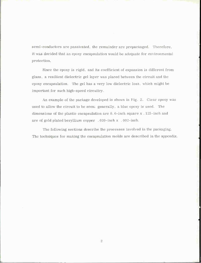
semi-conductors are passivated, the remainder are prepackaged. Therefore,
it was decided that an epoxy encapsulation would be adequate for environmental
protection.
Since the epoxy is rigid, and its coefficient of expansion is different from
glass, a resilient dielectric gel layer was placed between the circuit and the
epoxy encapsulation. The gel has a very low dielectric loss, which might be
important for such high-speed circuitry.
An example of the package developed is shown in Fig. 2. Clear epoxy was
used to allow the circuit to be seen; generally, a blue epoxy is used. The
dimensions of the plastic encapsulation are 0. 6-inch square x . 125-inch and
are of gold plated beryllium copper . 020-inch x . 002-inch.
The following sections describe the processes involved in the packaging.
The techniques for making the encapsulation molds are described in the appendix.

SEMI-CONDUCTOR CHIP
CONDUCTOR
RESISTOR
Fig. 1 . 'OR' Gate Ready for Leads
Fig. 2. Encapsulated Unit
3

SECTION II
TECHNIQUES
LEADS
The leads are etched in a comb pattern from beryllium copper sheet.
The patterns are then gold plated and appear as in Fig. 3. The outer surround-
ing portion of the comb serves to hold the individual leads in the right location,
while the inner ends are soldered to the circuit lands. All combs are made with
a total of 36 leads. For any particular circuit not requiring the full complement
of leads, the excess ones are cut with scissors.
Fig. 3. Lead Comb Ready for Attachment
When the inner ends of the leads have all been soldered to the circuit lands,
the excess material is clipped from the outer ends of the lands so that they
become electrically independent. A special clipping machine has been made to
cut the leads without distorting them or damaging the solder joint to the circuit.
When the leads have been attached, the circuits appear as in Fig. 4.

Fig. 4. 'Univer' Ready for Encapsulation
APPLICATION OF DIELECTRIC GEL
The circuits are supported by their leads on a slab of aluminum which
has a channel cut a little wider than the glass substrate.
Dow Corning Sylgard #51 is mixed according to instructions (a two-part
mix). Four drops of the gel are squeezed from an eye dropper onto each cir-
cuit. The liquid forms a smooth surfaced shallow mound over the circuit.
Surface tension prevents it running over the edges. The gel is cured at 75 C
overnight in an oven. It forms a sticky resilient layer. The gel is transparent,
so the circuit can be visually inspected for damage.

EPOXY ENCAPSULATION
A pair of mold halves is shown in Fig. 5 with a completed unit is one-half
of the mold. Also shown is the master for making the molds.
The middle white area of the mold halves consists of silicone rubber,
which has a certain amount of resilience. This rubber area contains the
molding cavity, the entry and overflow cavities, and the necessary gates between
them. The cavities have slightly raised ridges around their edges to reduce
flash, particularly between the leads.
The circuit, ready for encapsulation, is placed in the central cavity in
one of the mold halves. The circuit is supported by the leads resting on the
cavity edges. The circuit is carefully centered with the aid of a microscope.
The microscope has a grid reticle in the eyepiece. The reticle appears as a
. 050-inch grid superimposed on the mold. The mold is first moved to line up
the cavity sides on the grid, then the circuit is moved to line up the leads on
the correct grid lines. The second half of the mold is laid on the first and the
two clamped together with screws. The mold is then placed vertically in a
vise with the missing corner uppermost.
Stycast 1264 (Emerson and Cuming, Inc.) epoxy is used if transparent
encapsulation is required; otherwise opaque Stycast 2651 MM (Emerson and
Cuming, Inc. ) epoxy is used. While this can be obtained in black or most
colors, sky blue is generally used.
The epoxy is mixed according to the manufacturer's instructions and is
given a vacuum treatment to eliminate air bubbles. A disposable hypodermic
syringe (#18 gauge needle) is filled with the epoxy, then the needle is inserted
into the mold through the hole provided. Epoxy is slowly injected into the mold
until the overflow cavity is half filled. The hypodermic is removed, and a wire
plug inserted in the hypodermic hole.
6

5
c is

The mold is placed on a rack in an oven at 40 C and cured overnight.
When cured, the mold is opened. The superfluous epoxy pieces are easily
broken at the small gate sections. The molded encapsulation is shown in
Fig. 5. The package is lifted out of the mold. Sometimes a very thin flash
forms between the leads, but this flash can be easily removed with a pair of
tweezers. The unit then appears as in Fig. 2.
izkJk ti.e^tt Patrick Everett

APPENDIX
MOLD MAKING
Each half of a mold consists of two machined aluminum pieces (A and B
in Fig. 5). Part A is 1/8-inch thick and is cut in the form of a template.
Part B, 1/2-inch thick, has a 1/4-inch pin inserted and a 1/4-inch reamed
hole. The rubber section of each half-mold is made with the aid of the mold
master (C in Fig. 5).
The master is machined from brass. The two parts (D) which give the
main cavity in the molds are removable inserts. This allows the encapsulation
dimensions to be altered somewhat, if required, and the inserts can be polished
to give high quality molding.
The silicone rubber is Eccosil 4850 (Emerson and Cuming, Inc.). It is
mixed according to instructions and is given a vacuum treatment to remove air
bubbles. If the rubber is required to stick to the plates A and B, Eccosil
Primer 33 (Emerson and Cuming Inc. ), is applied first and allowed to dry.
Two aluminum parts (A) are laid on the master, using the pins and holes
as a guide; parts (E) on the master and the plates (A) then form an 1/8-inch
high wall around the mold details on the master. The silicone rubber is poured
over the mold details until the surface of the rubber is just over the tops of
plates (A). Plates (B) are then pressed down on top and the excess rubber
squeezed out between the plates.
The whole assembly is then cured in an oven at 40 C overnight. When
cured, the half-molds are lifted from the master, the gates are cut in the
rubber with a sharp knife, the two halves are then clamped together, and the
hole (F) for the hypodermic entry is drilled.
9

Before use, the aluminum parts of the mold are painted with a solution
of candle wax in xylene, to prevent any sticking of the epoxy. When a mold
becomes worn out or damage, the rubber is stripped out and the metal parts
are used again.
10
Security Classification
DOCUMENT CONTROL DATA • R&D (Security claaaillcatton ot till», body ot mbatract and indexing annotation muat c» entered whan the overall report ia clai allied)
1 ORIGINATING ACTIVITY (Corporate author) The MITRE Corporation Box 208 Bedford, Massachusetts
2«. REPORT seCURITV C L ASSI lrIC A TlON
Unclassified 2b GROUP
3 REPORT TITLE
Lead Attachment and Encapsulation Techniques for Thin Film Microcircuits
4 DESCRIPTIVE NOTES (Typ* ot report and Indue ive da tee)
N/A 5 AUTHORS (Laa t name, ft rat name, initial)
Everett, Patrick N.
6. REPORT DATE
February 1965 7# TOTAL NO. OP PAOEi
14 7b. NO. OF REPS
1 8«. CONTRACT OR ORANT NO.
AF19(628)-2390 b. PROJECT NO.
708 c
• • ORiaiNATOR't REPORT NUMBERS.)
ESD-TDR-64-630
lb OTHER REPORT NOfS; (A ny othat number* that may be aaalgnad
W-6353 10. AVAILAIILITY/LIMITATION NOTICES
Qualified requestors may obtain from DDC DDC release to OTS authorized.
11. SUPPLEMENTARY NOTES 12. SPONSORING MILITARY ACTIVITY Directorate of Computers L. G. Hanscom Field Bedford, Massachusetts
13. ABSTRACT
The techniques described were developed for encapsulating experi- mental thin film circuits deposited on 0. 5-inch square glass substrates. The encapsulation is epoxy, with final package dimensions of 0. 6-inch square x . 125-inch thick. Up to 32 ribbon leads emerge, on . 050 centers, arranged on the periphery of the package. A factor complica- ting the encapsulation was the requirement that the leads emerge on the four edges of the unit. A molding process using silicone rubber molds, and a hypodermic filling arrangement was evolved.
DD FORM 1 JAN 64 1473
Security Classification

Security Classification u
KEY WORDS LINK A
ROLE WT
LINK B
. HOL*
LINK C
NOLt
Electrical and Electronic Circuits Microcircuits Printed Circuits
Encapsulation Epoxy Plastics Dielectric Gel
INSTRUCTIONS
1. ORK 1NATING ACTIVITY: Enter the name and address of th* ontractor, subcontractor, grantee, Department of De- fense activity or other organization (corporate author) issuing the report.
2a. REPORT SECURITY CLASSIFICATION: Enter the over- all security classificstion of the report. Indicate whether "Restricted Data" is included* Marking is to be in accord- ance with appropriate security regulations.
26. GROUP: Automatic downgrading is specified in DoD Di- rective 5200.10 and Armed Forces Industrial Manual. Enter the group number. Also, when applicable, show that optional markings have been used for Group 3 and Group 4 as author- ized.
3. REPORT TITLE: Enter the complete report title in all capital lettera. Titles in all cases should be unclassified. If a meaningful title cannot be selected without classifica- tion, show title classification in all capitals in parenthesis immedistely following the title.
4. DESCRIPTIVE NOTES: If appropriate, enter the type of report, e.g., interim, progress, summary, annual, or final. Give the incluaive dates when a specific reporting period is covered. 5. AUTHOR(S): Enter the name(s) of authoKs) as shown on or in the report. Entei last name, first name, middle initial. If military, show rank and branch of service. The name of the principal author is an absolute minimum requirement.
6. REPORT DATE; Enter the date of the report as day, month, year; or month, year. If more than one date appears on the report, use date of publication. 7a. TOTAL NUMBER OF PAGES: The total page count should follow normal pagination procedures, Le., enter the number of pages containing information.
76. NUMBER OF REFERENCES: Enter the total number of references cited in the report. 8a. CONTRACT OR GRANT NUMBER: If appropriate, enter the applicable number of the contract or grant under which the report was written. 8b, 8c, & 8o*. PROJECT NUMBER: Enter the appropriate military department identification, such as project number, subproject number, system numbers, task number, etc
9a. ORIGINATOR'S REPORT NUMBER(S): Enter the offi- cial report number by which the document will be identified and controlled by the originating activity. This number must be unique to this report. 96. OTHER REPORT NUMBER(S): If the report has been assigned any other report numbers (either by the originator or by the sponsor), also enter this number^)«
10. AVAILABILITY/LIMITATION NOTICES: Enter any lim- itations on further dissemination of the report, other than those
imposed by security classification, using standard statementa such as:
(1) "Qualified requesters may obtain copies of this report from DDC."
(2) "Foreign announcement and dissemination of this report by DDC is not authorized."
(3) "U. S. Government agencies may obtain copies of this report directly from DDC. Other qualified DDC users shall request through
(4) "U. 8. military agencies may obtain copies of this report directly from DDC Other qualified users shall request through
(5) "All distribution of this report is controlled. Qual- ified DDC users shall request through
If the report has been furnished tc the Office of Technical Services, Department of Commerce, for sale to the public, indi- cate this fact and enter the price, if known.
1L SUPPLEMENTARY NOTES: Use for additional explana- tory notes.
12. SPONSORING MILITARY ACTIVITY: Enter the name of the departmental project office or laboratory sponsoring (pay ing for) the research and development. Include address.
13- ABSTRACT: Enter an abstract giving a brief and factual summary of the document indicative of the report, even though it may also appear elsewhere in the body of the technical re- port. If additional space is required, a continuation sheet shall be attached.
It is highly desirable that the abstract of classified reports be unclassified. Each paragraph of the abstract shall end with an indication of the military security classification of the in- formation in the paragraph, represented as (TS), (S). (C), or (U).
There is no limitation en the length of the abstract. How- ever, the suggested length is from 150 to 225 words.
14. KEY WORDS: Key words are technically meaningful terms or short phrases that characterize a report and may be used aa index entries for cataloging the report. Key words must be selected so that no security classification is required. Identi- fiers, such as equipment model designation, trade name, military project code name, geographic location, may be uaed as key words but will be followed by an indication of technical con- text. The assignment of links, roles, and weights is optional
Security Classification