Lcd samsung sp20 so la20s51b
28
TFT-LCD TV Chassis Model SP20SO LA20S51B Manual SERVICE TFT-LCD TV CONTENTS 1. Precautions 2. Product Specifications 3. Disassembly & Reassembly 4. Alignment & Adjustments 5. Troubleshooting 6. Exploded View & Parts List 7. Electrical Parts List 8. Block Diagram 9. Wiring Diagram 10. PCB Layout 11. Schematic Diagrams 12. Panel Description
-
Upload
soyneo2 -
Category
Technology
-
view
544 -
download
4
Transcript of Lcd samsung sp20 so la20s51b

TFT-LCD TVChassis ModelSP20SO LA20S51B
ManualSERVICETFT-LCD TV CONTENTS
1. Precautions
2. Product Specifications
3. Disassembly & Reassembly
4. Alignment & Adjustments
5. Troubleshooting
6. Exploded View & Parts List
7. Electrical Parts List
8. Block Diagram
9. Wiring Diagram
10. PCB Layout
11. Schematic Diagrams
12. Panel Description
2 Product Specifications
2-2
123456789
101112131415
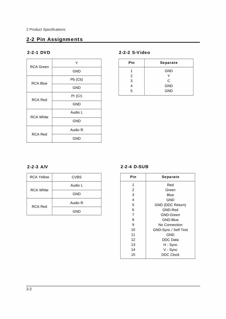
2-2 Pin Assignments
RCA Green
RCA Blue
RCA Red
RCA White
RCA Red
Y
GND
Pb (Cb)
GND
Pr (Cr)
GND
Audio L
GND
Audio R
GND
2-2-1 DVD
RCA White
RCA Red
CVBS
Audio L
GND
Audio R
GND
2-2-3 A/V
RCA Yellow
Pin Separate
12345
GNDYC
GNDGND
2-2-2 S-Video
Pin Separate
RedGreenBlueGND
GND (DDC Return)GND-Red
GND-GreenGND-Blue
No ConnectionGND-Sync / Self Test
GNDDDC DataH - SyncV - Sync
DDC Clock
2-2-4 D-SUB

2 Product Specifications
2-3
Separate Sync
2-3 Timing Chart
This section of the service manual describes the timing that the computer industry recognizes as standard forcomputer-generated video signals.
C D
A O
E
B P
Video
Sync Sync
Video
Q R S
A : Line time total B : Horizontal sync width O : Frame time total P : Vertical sync width
C : Back porch D : Active time Q : Back porch R : Active time
E : Front porch S : Front porch
H/V Composite Sync
Sync-on-Green
79.976
12.504
1.067
1.837
9.481
0.119
75.025
13.329
0.038
0.475
12.804
1280/75Hz,50Hz1280x1024
1024/75Hz1024 x 768
60.023
16.660
1.219
2.235
13.003
0.203
75.029
13.328
0.050
0.466
12.795
0.017
78.750
Positive
Positive
Separate
31.469
31.777
3.813
1.589
26.058
0.318
70.087
14.268
0.064
0.858
13.155
0.191
28.322
Negative
Positive
Separate
µ
µ
µ
µ
µ
IBM
640/75 Hz, 60Hz, 72Hz640 x 480
800/75 Hz, 56Hz,60Hz, 72Hz800 x 600
1024/60Hz1024 x 768
VGA2/70 Hz720 x 400
VGA3/60 Hz640 x 480
Table 2-1 Timing Chart
31.469
31.778
3.813
1.589
26.058
0.318
59.940
16.683
0.064
0.794
15.761
0.064
25.175
Negative
Negative
Separate
37.500
26.667
2.032
3.810
20.317
0.508
75.000
13.333
0.080
0.427
12.800
0.027
31.500
Negative
Negative
Separate
46.875
21.333
1.616
3.232
16.162
0.323
75.000
13.333
0.064
0.448
12.800
0.021
49.500
Positive
Positive
Separate
48.363
20.677
2.092
2.462
15.754
0.369
60.004
16.666
0.124
0.600
15.880
0.062
75.000
Negative
Negative
Separate
Mode VESA
Timing
3 Disassembly and Reassembly
3-1
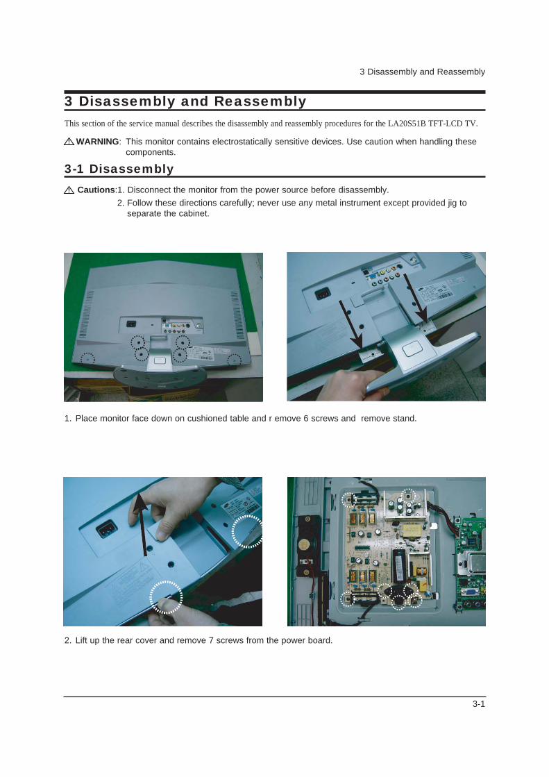
3 Disassembly and ReassemblyThis section of the service manual describes the disassembly and reassembly procedures for the LA20S51B TFT-LCD TV.
WARNING: This monitor contains electrostatically sensitive devices. Use caution when handling thesecomponents.
3-1 DisassemblyCautions:1. Disconnect the monitor from the power source before disassembly.
2. Follow these directions carefully; never use any metal instrument except provided jig toseparate the cabinet.
1. Place monitor face down on cushioned table and r emove 6 screws and remove stand.
2. Lift up the rear cover and remove 7 screws from the power board.

3 Disassembly and Reassembly
3-2
3. Remove 8 screws from the main board and disconnect cables.
4. Lift up the power board and main board.
5. Remove 6 screws from the BRKT and lift up the BRKT.
3 Disassembly and Reassembly
3-3
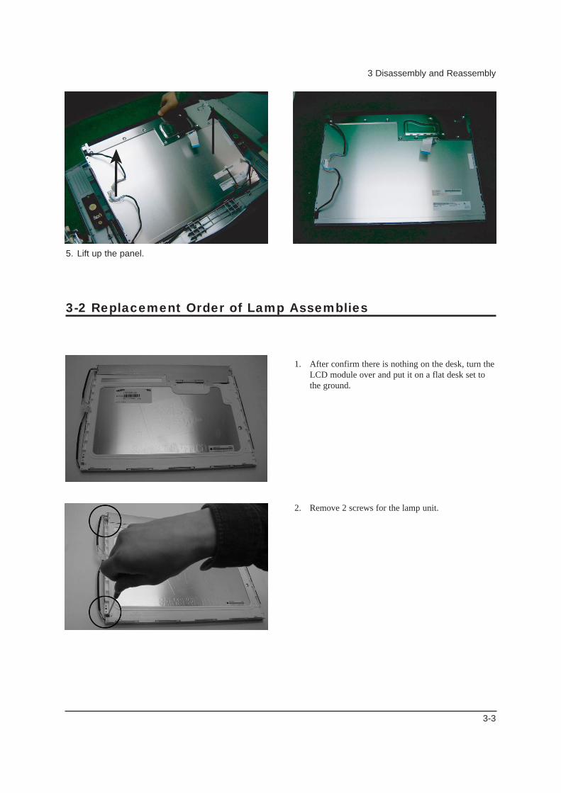
1. After confirm there is nothing on the desk, turn theLCD module over and put it on a flat desk set tothe ground.
2. Remove 2 screws for the lamp unit.
3-2 Replacement Order of Lamp Assemblies
5. Lift up the panel.

3 Disassembly and Reassembly
3-4
3 Disassembly and Reassembly
3-4
3-3 Reassembly
Reassembly procedures are in the reverse order of disassembly procedures.
4. Please fix the new lamp units on the LCD module :opposite process 2 and 3.
3. Slide the lamp unit out. Please take out the lampunit from the LCD module.
Slide the lamp unit out.
Slide the lamp unit out.

4 Alignments and Adjustments
4-1
4 Alignments and Adjustments
4-1 General Alignment Instuction1. Usually, a color LCD TV needs only slight touch-up adjustment upon installation.
Check the basic characteristics such as height, horizontal and vertical sync.
2. Use the specified test equipment or its equivalent.
3. Correct impedance matching is essential.
4. Avoid overload. Excessive signal from a sweep generator might overload the front-end of the TV. When inserting signal markers, do not allow the marker generator to distort test result.
5. Connect the TV only to an DC power source with voltage and frequency as specified on
the backcover nameplate.
6. Do not attempt to connect or disconnect any wire while the TV is turned on. Make sure that the power cord is disconnected before replacing any parts.
7. To protect aganist shock hazard, use an isolation transform.

4-2 Factory Mode Adjustments
4-2-1 Entering Factory Mode1. To enter “Service Mode” Press the remote -control keys in this sequence :
- If you do not have Factory remote - control
- If you have Factory remote - control
4-2-2 Factory Mode Tree
4 Alignments and Adjustments
4-2

4 Alignments and Adjustments
4-3

4 Alignments and Adjustments
4-4
4 Alignments and Adjustments
4-5
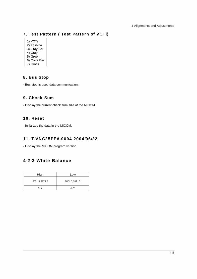
7. Test Pattern ( Test Pattern of VCTi)1) VCTi2) Toshiba3) Gray Bar4) Gray5) Green6) Color Bar7) Cross
8. Bus Stop- Bus stop is used data communication.
9. Chcek Sum- Display the current check sum size of the MICOM.
10. Reset- Initializes the data in the MICOM.
11. T-VNC25PEA-0004 2004/06/22 - Display the MICOM program version.
4-2-3 White Balance
High Low
263 5, 267 5 267 5, 263 5
x, y x, y

4-2-4 Calibration
4 Alignments and Adjustments
4-6

5 Troubleshooting
5-1
5 Troubleshooting
5-1 No Power
Does proper DC 14V/5Vappear at Pin 3. Pin 9 of
CN100?
Check CN803 Pin3, Pin9 in I/PBoard.
Yes
No
No
No
No
No
Does proper DC A5V appear at FT144? Check IC101 and IC105.
Yes
Does proper B3.3V appear at Pin 2 of IC111? Check IC111.
Yes
Does proper DC B1.8V appear at Pin 4 of IC112? Check IC112.
Yes
Does proper DC B8V appear at FT130? Check IC109.
1
2
3
4
5
5 Troubleshooting
5-2
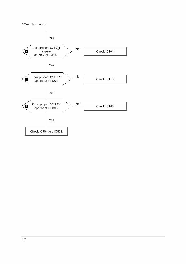
No
No
No
Check IC704 and IC802.
Yes
Does proper DC 5V_Pappear
at Pin 2 of IC104?Check IC104.
Yes
Does proper DC 9V_Sappear at FT127? Check IC110.
Yes
Yes
Does proper DC B5Vappear at FT131? Check IC108.
6
7
8

5 Troubleshooting
5-3
WAVEFORMS
1 2
5
3
644
7 8
5 Troubleshooting
5-4
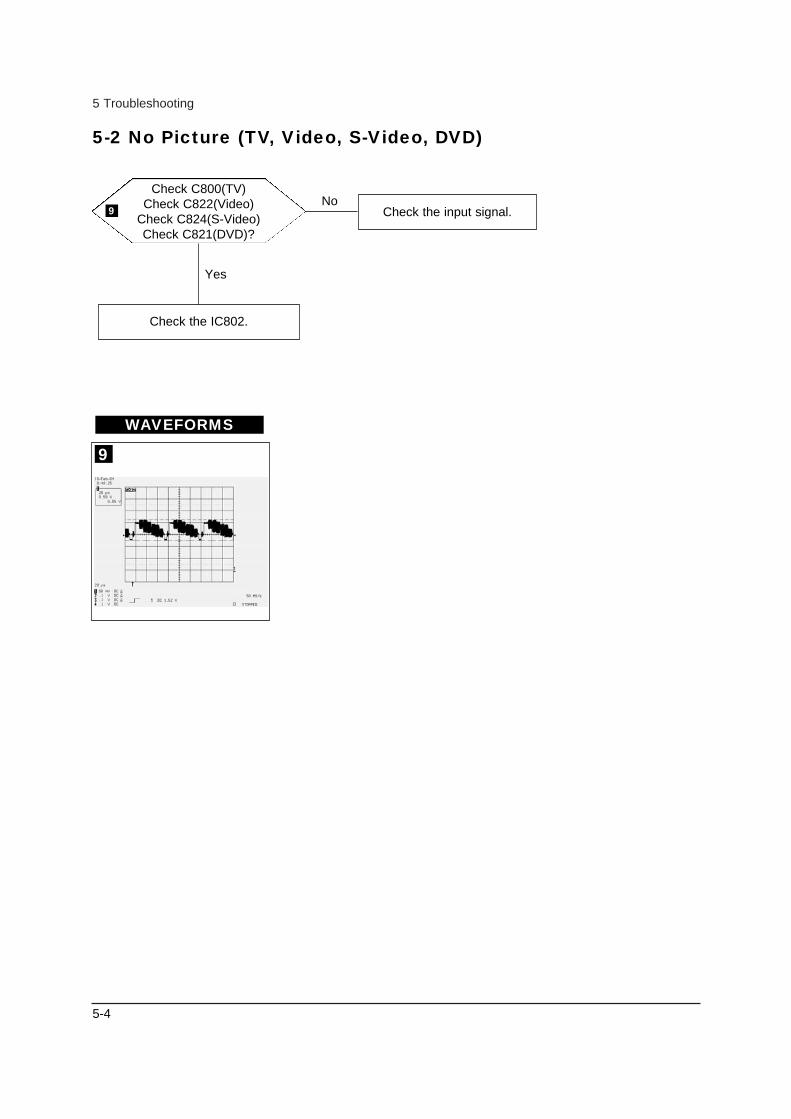
5-2 No Picture (TV, Video, S-Video, DVD)
Check C800(TV)Check C822(Video)
Check C824(S-Video)Check C821(DVD)?
Check the input signal.
Yes
Check the IC802.
WAVEFORMS
9
9No
5 Troubleshooting
5-5
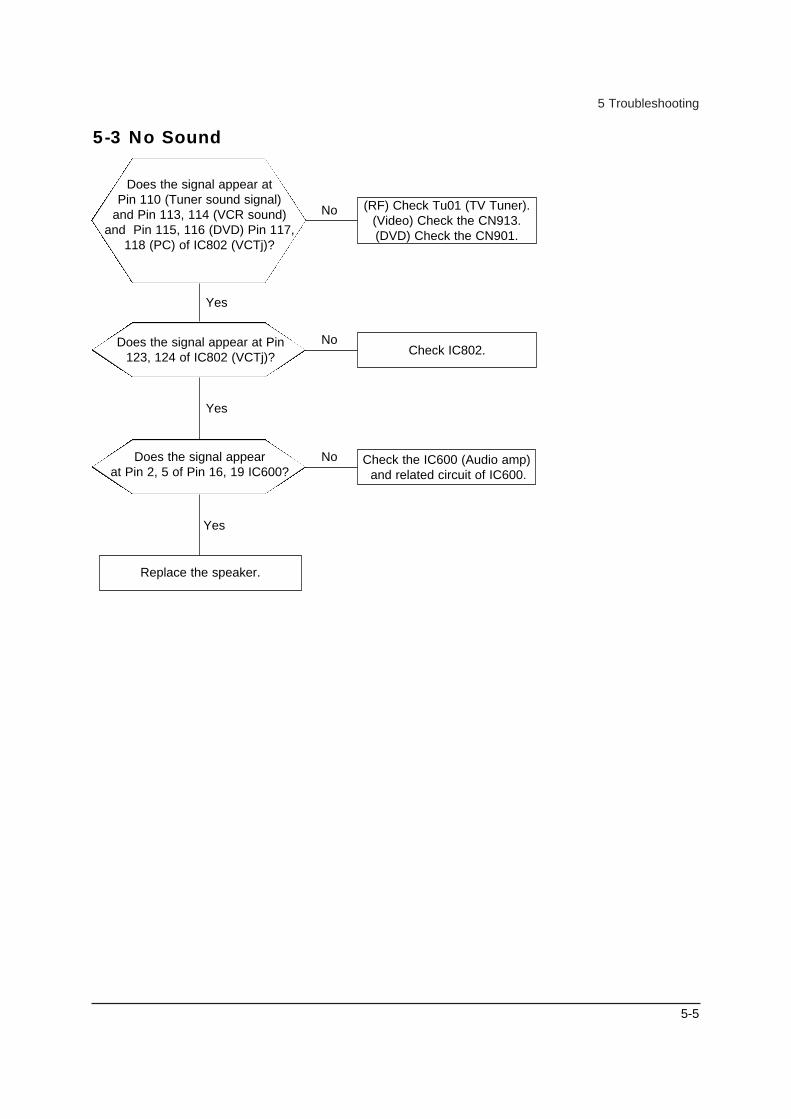
Does the signal appear at Pin 110 (Tuner sound signal)
and Pin 113, 114 (VCR sound) and Pin 115, 116 (DVD) Pin 117,
118 (PC) of IC802 (VCTj)?
(RF) Check Tu01 (TV Tuner).(Video) Check the CN913.(DVD) Check the CN901.
Yes
Does the signal appear at Pin123, 124 of IC802 (VCTj)? Check IC802.
Yes
Does the signal appear at Pin 2, 5 of Pin 16, 19 IC600?
Check the IC600 (Audio amp)and related circuit of IC600.
Yes
Replace the speaker.
5-3 No Sound
No
No
No

8 Block Diagrams
8-1
8 Block Diagram- This Document can not be used without Samsung’s authorization.
8-1 Signal Path Block Diagram
8 Block Diagrams
8-2
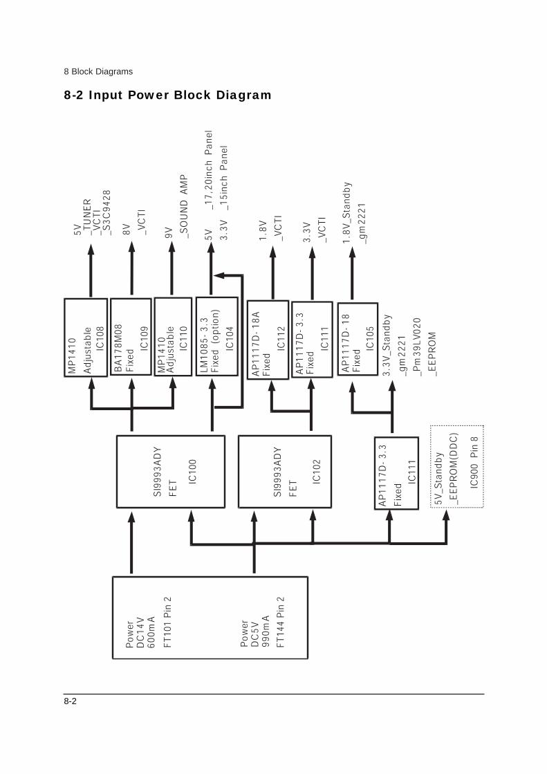
8-2 Input Power Block Diagram

10 PCB Layout
10-1
10 PCB Layout10-1 Main PCB Layout
D601 DIODE-ARRAY 143.6 142.7 D907 DIODE-ARRAY 11.0 22.8 D101 DIODE-RECTIFIER 43.8 117.7 D102 DIODE-RECTIFIER 104.7 140.8 D200 DIODE-SWITCHING 156.3 110.5 D600 DIODE-SWITCHING 124.7 140.2 D701 DIODE-SWITCHING 20.9 88.5 D702 DIODE-SWITCHING 45.4 81.9 D800 DIODE-SWITCHING 66.0 104.5 D908 DIODE-SWITCHING 24.9 45.1 D909 DIODE-SWITCHING 25.5 40.4 D910 DIODE-SWITCHING 31.9 40.4 D912 DIODE-SWITCHING 17.1 22.8 D913 DIODE-SWITCHING 24.6 22.7 D915 DIODE-SWITCHING 149.6 26.3 D948 DIODE-SWITCHING 100.8 33.9 D949 DIODE-SWITCHING 97.6 38.7 D951 DIODE-SWITCHING 4.2 87.9 D952 DIODE-SWITCHING 3.1 83.4 D953 DIODE-SWITCHING 7.3 84.2 D954 DIODE-SWITCHING 3.1 79.0 D955 DIODE-SWITCHING 7.3 75.4 D956 DIODE-SWITCHING 3.1 73.5 D957 DIODE-SWITCHING 6.9 71.1 D602 DIODE-ZENER 149.8 144.8 D904 DIODE-ZENER 51.3 41.5 D916 DIODE-ZENER 149.5 17.7 D917 DIODE-ZENER 3.0 40.2 D918 DIODE-ZENER 16.8 39.9 D919 DIODE-ZENER 8.6 40.2 D920 DIODE-ZENER 149.5 21.9 D928 DIODE-ZENER 2.2 27.6 D950 DIODE-ZENER 153.5 26.0 D201 DIODE-ZENER 141.4 86.4 D603 DIODE-ZENER 155.0 116.3 D604 DIODE-ZENER 148.1 116.2 D900 DIODE-ZENER 106.9 39.0 D901 DIODE-ZENER 110.6 33.5 D902 DIODE-ZENER 59.7 22.2 D903 DIODE-ZENER 82.8 27.0 D905 DIODE-ZENER 55.7 22.1 D906 DIODE-ZENER 78.5 22.2 D911 DIODE-ZENER 6.2 57.9 D914 DIODE-ZENER 13.9 57.9 D921 DIODE-ZENER 73.2 41.4 D922 DIODE-ZENER 73.2 43.7 D923 DIODE-ZENER 73.3 48.5 D924 DIODE-ZENER 73.2 46.2 D925 DIODE-ZENER 55.2 41.5 D926 DIODE-ZENER 111.2 33.7 D927 DIODE-ZENER 103.2 38.3 D930 DIODE-ZENER 71.2 22.2 D932 DIODE-ZENER 82.5 13.6 D934 DIODE-ZENER 82.5 17.9 D936 DIODE-ZENER 67.0 22.1 D940 DIODE-ZENER 31.4 22.3
Loc. No. Description X
D941 DIODE-ZENER 35.5 22.3 D942 DIODE-ZENER 40.8 22.2 D945 DIODE-ZENER 37.7 36.1 D946 DIODE-ZENER 100.7 28.4 D947 DIODE-ZENER 95.3 23.4 D944 DIODE-ZENER 44.9 22.2
IC600 IC-AUDIO AMP 134.7 125.6 IC601 IC-AUDIO AMP 148.8 129.2 IC902 IC-CMOS LOGIC 28.8 51.4 IC903 IC-CMOS LOGIC 28.6 51.2 IC108 IC-DC/DC CONVERTER 42.1 127.8 IC110 IC-DC/DC CONVERTER 107.2 151.3 IC900 IC-EEPROM 4.5 18.0 IC705 IC-EEPROM 32.4 85.7 IC805 IC-EEPROM 72.7 80.7 IC703 IC-FLASH MEMORY 0.0 0.0 IC704 IC-LCD CONTROLLER 25.8 81.3 IC109 IC-POSI.FIXED REG. 53.8 134.9 IC706 IC-REAL TIME CLOCK 4.8 104.4 IC500 IC-VIDEO SWITCH 43.8 49.1 IC501 IC-VIDEO SWITCH 50.4 59.0 IC300 IC-VOL. DETECTOR 105.2 60.6 IC105 IC-VOLTAGE REGULATOR 49.1 108.6 IC112 IC-VOLTAGE REGULATOR 117.4 120.2 IC101 IC-VOLTAGE REGULATOR 114.1 132.7 IC111 IC-VOLTAGE REGULATOR 107.0 118.4
Q200 TR-SMALL SIGNAL 146.5 110.4 Q600 TR-SMALL SIGNAL 156.3 138.1 Q601 TR-SMALL SIGNAL 150.5 140.8 Q602 TR-SMALL SIGNAL 139.5 142.7 Q603 TR-SMALL SIGNAL 129.3 140.2 Q800 TR-SMALL SIGNAL 87.6 62.0 Q902 TR-SMALL SIGNAL 149.7 26.0 Q100 TR-SMALL SIGNAL 14.9 119.9 Q101 TR-SMALL SIGNAL 14.4 128.1 Q104 TR-SMALL SIGNAL 16.6 132.9 Q805 TR-SMALL SIGNAL 62.6 104.5 Q810 TR-SMALL SIGNAL 56.4 83.2 Q900 TR-SMALL SIGNAL 149.6 31.2 Q901 TR-SMALL SIGNAL 145.6 31.2 Q801 TR-SMALL SIGNAL 91.5 62.2 Q802 TR-SMALL SIGNAL 53.1 97.5 Q803 TR-SMALL SIGNAL 53.1 101.4 Q804 TR-SMALL SIGNAL 57.1 106.5 Q809 TR-SMALL SIGNAL 131.7 99.7
TRANSISTOR
IC
Loc. No. Description X
DIODE

9-1
9 Schematic Diagrams
9 Wiring Diagram
11-1
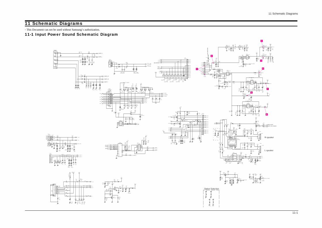
11 Schematic Diagrams
11 Schematic Diagrams- This Document can not be used without Samsung’s authorization.
11-1 Input Power Sound Schematic Diagram

11 Schematic Diagrams
11-2
1 2
5
3
6
4
7 8
11 Schematic Diagrams
9

11-3
11 Schematic Diagrams
- This Document can not be used without Samsung’s authorization.
11-2 Video Decoder Schematic Diagram

11-5
11 Schematic Diagrams
- This Document can not be used without Samsung’s authorization.
11-3 Output Scaler, LVDS Schematic Diagram
11 Schematic Diagrams
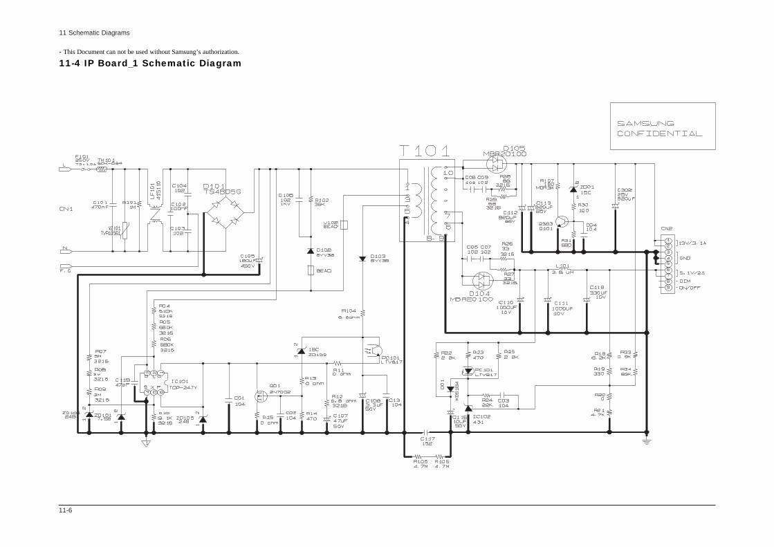
11-6
- This Document can not be used without Samsung’s authorization.
11-4 IP Board_1 Schematic Diagram

11-7
11 Schematic Diagrams
- This Document can not be used without Samsung’s authorization.
11-7 IP Board_2 Schematic Diagram


![SAMSUNG LCD Service Manual Internal] _ ES15U](https://static.fdocuments.us/doc/165x107/551286fc4a7959c4028b49c9/samsung-lcd-service-manual-internal-es15u.jpg)


![Samsung Gtn32se Chassis Le32a43t Lcd [ET]](https://static.fdocuments.us/doc/165x107/547f5644b379595e2b8b582d/samsung-gtn32se-chassis-le32a43t-lcd-et.jpg)