LCD Datasheet By Beyondinfinite · -1-1. Application This data sheet defines the ... SYMBOL...
29
Transcript of LCD Datasheet By Beyondinfinite · -1-1. Application This data sheet defines the ... SYMBOL...


- 1 -
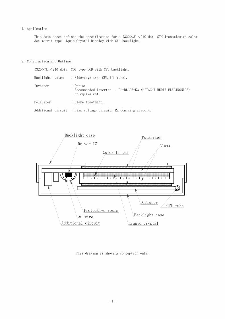
1. Application
This data sheet defines the specification for a (320ѱ3)ѱ240 dot, STN Transmissive colordot matrix type Liquid Crystal Display with CFL backlight.
2. Construction and Outline
(320ѱ3)ѱ240 dots, COB type LCD with CFL backlight.
Backlight system : Side-edge type CFL (ɠ tube).
Inverter : Option.Recommended Inverter ϖ PH-BLC08-K3 (HITACHI MEDIA ELECTRONICS)or equivalent.
Polarizer : Glare treatment.
Additional circuit : Bias voltage circuit, Randomizing circuit.
This drawing is showing conception only.
Protective resin
Color filter
Additional circuit
Au wire
Driver IC
Backlight casePolarizer
Backlight case
DiffuserCFL tube
Liquid crystal
Glass
BGRBGRBGRBGR
- 2 -
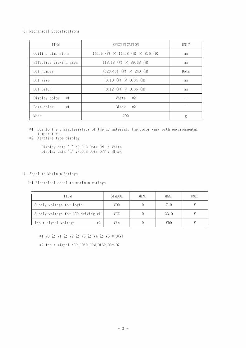
3. Mechanical Specifications
ITEM SPECIFICATION UNIT
Outline dimensions 154.6 (W) ѱ 114.8 (H) ѱ 8.5 (D) mm
Effective viewing area 118.18 (W) ѱ 89.38 (H) mm
Dot number (320ѱ3) (W) ѱ 240 (H) Dots
Dot size 0.10 (W) ѱ 0.34 (H) mm
Dot pitch 0.12 (W) ѱ 0.36 (H) mm
Display color *1 White *2 ҥ
Base color *1 Black *2 ҥ
Mass 200 g
*1 Due to the characteristics of the LC material, the color vary with environmentaltemperature.
*2 Negative-type display
Display data "H" :R,G,B Dots ON : WhiteDisplay data "L" :R,G,B Dots OFF : Black
4. Absolute Maximum Ratings
4-1 Electrical absolute maximum ratings
ITEM SYMBOL MIN. MAX. UNIT
Supply voltage for logic VDD 0 7.0 V
Supply voltage for LCD driving *1 VEE 0 33.0 V
Input signal voltage *2 Vin 0 VDD V
*1 V0 ғ V1 ғ V2 ғ V3 ғ V4 ғ V5 = 0(V)
*2 Input signal :CP,LOAD,FRM,DISP,D0ϡD7

- 3 -
4-2 Environmental absolute maximum ratings
ITEM SYMBOL MIN MAX UNIT
Operating temperature *1 Top 0 60 ѵ
Storage temperature *2 T -20 60 ѵɻɼɷ
Operating humidity *3 Hop 10 *4 %RH
Storage humidity *3 H 10 *4 %RHɻɼɷ
Vibration ҥ *5 *5 ҥ
Shock ҥ *6 *6 ҥ
*1 LCD's display quality shall not be guaranteed at the temperature rangeof : below 0ѵ and upper 40ѵ.
*2 Temp. = -20ѵ Ҧ 48 h , Temp = 60ѵ Ҧ 168 hStore LCD panel at normal temperature/humidity. Keep it free fromvibration and shock. LCD panel that is kept at low or high temperaturefor a long time can be defective due to the other conditions, even ifthe temperature satisfies standard.
*3 Non-condensation.
*4 Temp. Ғ 40ѵ, 85ҡ RH Max.Temp. Ҩ 40ѵ, Absolute Humidity shall be less than 85ҡRH at 40ѵ.
*5Frequency 10ϡ55 Hz Converted to
acceleration value :Vibration width 0.15 mm ϑ0.3ϡ9 m/sϒ2
Interval 10-55-10 Hz 1 minute
2 hours in each direction X/Y/Z (6 hours as total)EIAJ ED-2531
2*6 Acceleration: 490m/sPulse width : 11 ms3 times in each direction : ѰX/ѰY/ѰZ.EIAJ ED-2531

- 4 -
5. Electrical Characteristics
Temp. = 25ѵ, VDD = +5.0V Ѱ 5%
ITEM SYMBOL CONDITION MIN. TYP. MAX. UNIT
Supply voltage for logic VDD ҥ 4.75 5.00 5.25 V
LCD driving voltage *1 Vop= 0 ѵ 25.4 26.4 27.4 V
VEE 25 ѵ 24.4 25.4 26.4 V
60 ѵ 22.6 23.6 24.6 V
Input voltage Vin "H" level 0.8VDD ҥ VDD V
"L" level 0 ҥ 0.2VDD V
Clock frequency ʈcp 2.02 2.16 16.0 MHz
Frame frequency *2 ʈ 70 75 80 Hzɮɺɵ
Current consumption IDD ҥ 3.0 4.5 mAfor logic
Current consumption IEE *3 ҥ 7.5 11.3 mAfor LCD driving
Power consumption Pdisp ҥ 210 325 mW
*1 Maximum contrast ratio is obtained by adjusting the LCD supply voltage( Vop= VEE ) for driving LCD.
*2 In consideration of display quality, it is recommended that frame frequency is set inthe range of 70-80Hz. When you have to use higher frame and clock frequencies, confirmthe LCD's performance and quality prior to finalizing the frequency values: Generally,as frame and clock frequencies become higher current consumption will get bigger anddisplay quality will be degraded.
*3 Display high frequency pattern, ( see below ).VDD = 5.0V , Vop = VEE , ʈ = 75 Hz , fcp = 2.16MHzɮɺɵ
Pattern:
ɠ ɡ ɢ ɣ ɤ ɥ ɨɥɟϑʆʑʖϒ
ӕӖӕӖӕӖӕӖӕӖӕӖӕӖӕӖӕӖӕӖɠ
ӖӕӖӕӖӕӖӕӖӕӖӕӖӕӖӕӖӕӖӕɡ
ӕӖӕӖӕӖӕӖӕӖӕӖӕӖӕӖӕӖӕӖɢ
ӖӕӖӕӖӕӖӕӖӕӖӕӖӕӖӕӖӕӖӕϖ
ӕӖӕӖӕӖӕӖӕӖӕӖӕӖӕӖӕӖӕӖϖ
ӖӕӖӕӖӕӖӕӖӕӖӕӖӕӖӕӖӕӖӕɡɢɨ
ӕӖӕӖӕӖӕӖӕӖӕӖӕӖӕӖӕӖӕӖɡɣɟ
ϑʆʑʖϒ

- 5 -
ɥϔOptical Characteristics
Temp. = 25ѵ
ITEM SYMBOL CONDITION MIN. TYP. MAX. UNIT
Response Rise Tr ==0ѯ ҥ 220 320 mstime
Down Td ==0ѯ ҥ 110 210 ms
Viewing angle range =0Л (-50) ҥ (40) deg.CRғ2
=0Л (-50) ҥ (50) deg.
Contrast ratio CR ==0ѯ 20.0 40.0 ҥ ҥ
2Brightness(IL=5.0mA) L ҥ 140 200 ҥ cd/m
Chromaticity Red x 0.50 0.55 0.60coordinates ==0ѯ
y 0.30 0.35 0.40
Green x 0.26 0.31 0.36==0ѯ
y 0.47 0.52 0.57
Blue x 0.11 0.16 0.21==0ѯ ҥ
y 0.12 0.17 0.22
White x 0.27 0.32 0.37==0ѯ
y 0.30 0.35 0.40
Black x 0.25 0.30 0.35==0ѯ
y 0.26 0.31 0.36
Optimum contrast is obtained by adjusting the LCD driving voltage(Vop)while at the viewing angle of = = 0ѯ.
6-1 Contrast ratio is defined as follows:
Brightness all pixels "White"CR =
Brightness all pixels "Black"
- 6 -
6-2. Definition of Vop
6-3. Definition of response time
VVVVEEEEEEEE ((((VVVV))))VVVVoooopppp
CCCCoooonnnnttttrrrraaaasssstttt
CCCCRRRR mmmmaaaaxxxx
- 7 -
6-4. Definition of viewing angle
6-5. Measuring points
80ѱ3 160ѱ3 240ѱ3 (dot)
1 4
60 ӝ ӝ
3
120 ӝ
2 5
180 ӝ ӝ
(dot)
1) Rating is defined as the average brightness inside the viewing area.
2) 30 minutes after CFL is turned on. (Ambient Temp.=25ѵ)
3) The inverter should meet the eccentric conditions;
-Sine, symmetric waveform without spike in positive and negative.
4) Measuring Inverter : PH-BLC08-K3(HITACHI MEDIA ELECTRONICS)
- 8 -
ɦ. Circuit Block Diagram of LCD
SEGMENTDRIVERIC
(320ѱ3)ѱ240LCD
1/240duty
FRM
VDD,VSS
DISP
LOAD
CP
D0ϡD7
COMMON DRIVER IC
*1 COMIC
SEGIC
VEE
*2
*1Randomizingcircuit
*2Biasvoltagecircuit
- 9 -
7-1. Power supply
TrVEE
VRVop ɳɫɻɟɤɦɹɾɠɩ
+5.0V VDD
VSS
- 10 -
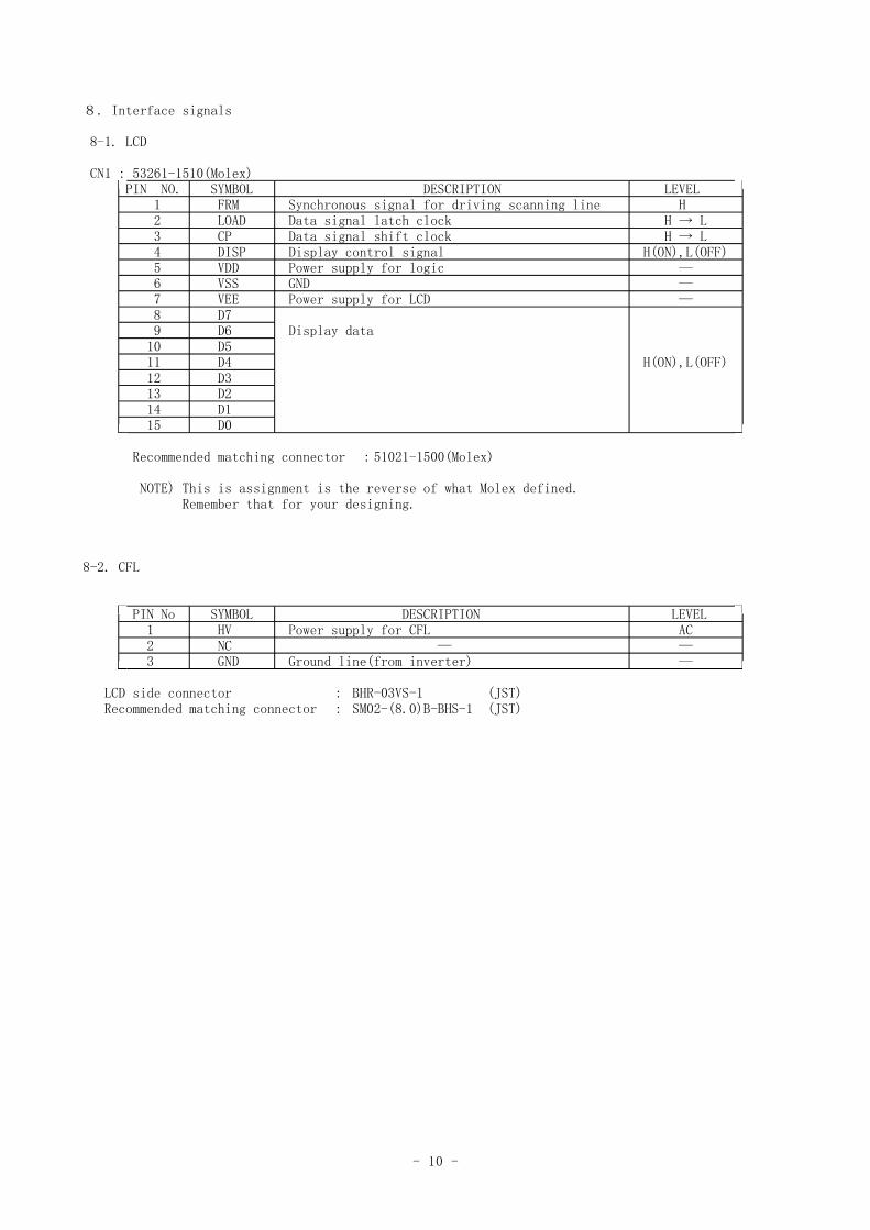
ɧ. Interface signals
8-1. LCD
CN1 : 53261-1510(Molex)PIN NO. SYMBOL DESCRIPTION LEVEL
1 FRM Synchronous signal for driving scanning line H2 LOAD Data signal latch clock H ҳ L3 CP Data signal shift clock H ҳ L4 DISP Display control signal H(ON),L(OFF)5 VDD Power supply for logic ;6 VSS GND ;7 VEE Power supply for LCD ;8 D79 D6 Display data10 D511 D4 H(ON),L(OFF)12 D313 D214 D115 D0
Recommended matching connector ϖ51021-1500(Molex)
NOTE) This is assignment is the reverse of what Molex defined.Remember that for your designing.
8-2. CFL
PIN No SYMBOL DESCRIPTION LEVEL1 HV Power supply for CFL AC2 NC ; ;3 GND Ground line(from inverter) ;
LCD side connector ϖ BHR-03VS-1 (JST)Recommended matching connector ϖ SM02-(8.0)B-BHS-1 (JST)
- 11 -
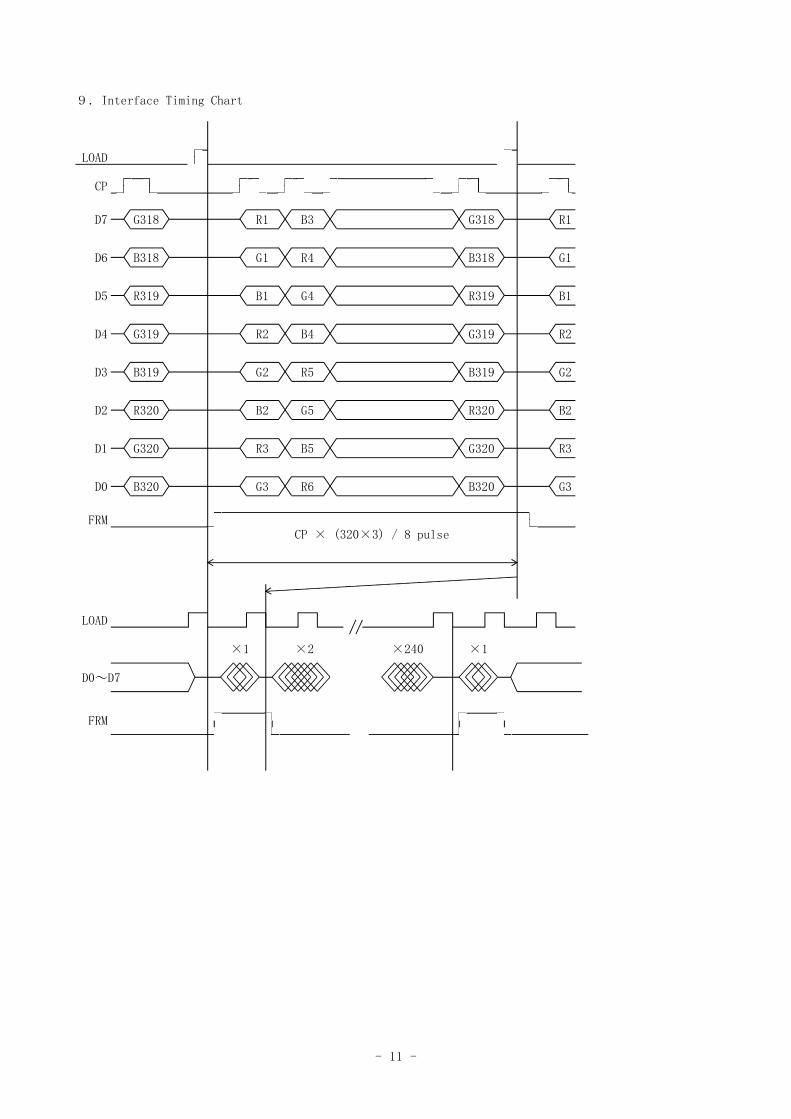
ɨϔInterface Timing Chart
LOAD
CP
D7 G318 R1 B3 G318 R1
D6 B318 G1 R4 B318 G1
D5 R319 B1 G4 R319 B1
D4 G319 R2 B4 G319 R2
D3 B319 G2 R5 B319 G2
D2 R320 B2 G5 R320 B2
D1 G320 R3 B5 G320 R3
D0 B320 G3 R6 B320 G3
FRMCP ѱ (320ѱ3) / 8 pulse
LOAD
ѱ1 ѱ2 ѱ240 ѱ1
D0ϡD7
FRM
- 12 -
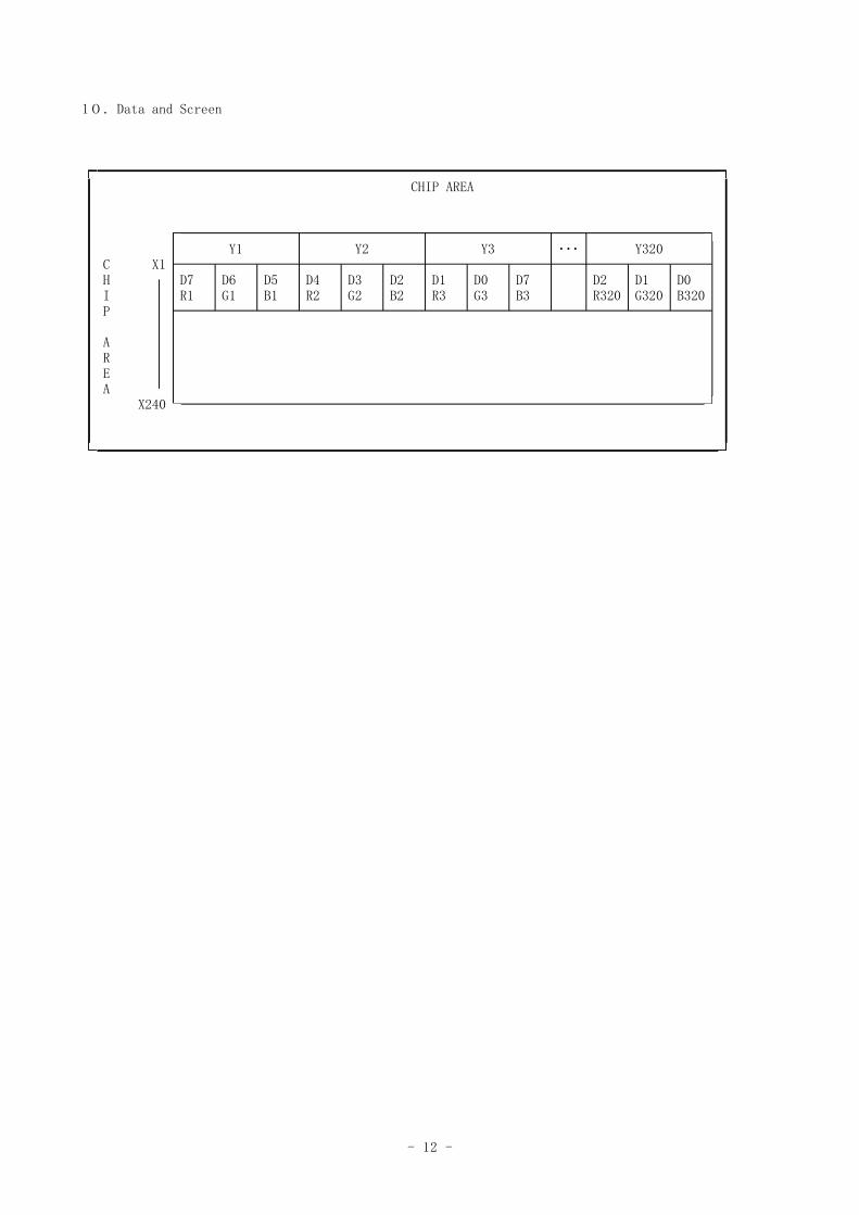
1ɟϔData and Screen
CHIP AREA
Y1 Y2 Y3 ]]] Y320C X1H D7 D6 D5 D4 D3 D2 D1 D0 D7 D2 D1 D0I R1 G1 B1 R2 G2 B2 R3 G3 B3 R320 G320 B320P
AREA
X240

- 13 -
ɠɠ.Input Timing Characteristics of LCD
trCP tfCPtWCLH tWCLL tCCL
ɫɸ
tDS tDHɬɩɼɩ
ɫɸ
last 1st 1sttCL tLC
tWLPHtLCL
ɴɷɩɬ
tWLPLtr tf
tFS tFHɮɺɵ
- 14 -
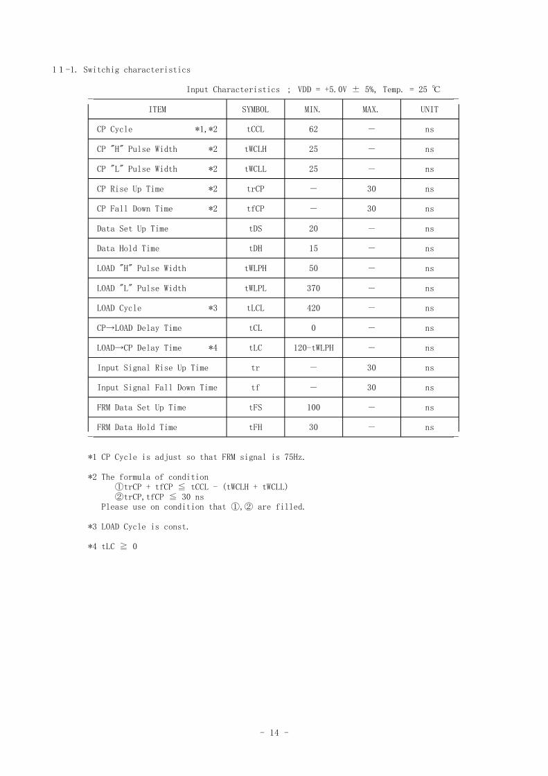
1ɠ-1. Switchig characteristics
Input Characteristics ϗ VDD = +5.0V Ѱ 5%, Temp. = 25 ѵ
ITEM SYMBOL MIN. MAX. UNIT
CP Cycle *1,*2 tCCL 62 ҥ ns
CP "H" Pulse Width *2 tWCLH 25 ҥ ns
CP "L" Pulse Width *2 tWCLL 25 ҥ ns
CP Rise Up Time *2 trCP ҥ 30 ns
CP Fall Down Time *2 tfCP ҥ 30 ns
Data Set Up Time tDS 20 ҥ ns
Data Hold Time tDH 15 ҥ ns
LOAD "H" Pulse Width tWLPH 50 ҥ ns
LOAD "L" Pulse Width tWLPL 370 ҥ ns
LOAD Cycle *3 tLCL 420 ҥ ns
CPҳLOAD Delay Time tCL 0 ҥ ns
LOADҳCP Delay Time *4 tLC 120-tWLPH ҥ ns
Input Signal Rise Up Time tr ҥ 30 ns
Input Signal Fall Down Time tf ҥ 30 ns
FRM Data Set Up Time tFS 100 ҥ ns
FRM Data Hold Time tFH 30 ҥ ns
*1 CP Cycle is adjust so that FRM signal is 75Hz.
*2 The formula of conditionΟtrCP + tfCP Ғ tCCL - (tWCLH + tWCLL)ΠtrCP,tfCP Ғ 30 ns
Please use on condition that Ο,Π are filled.
*3 LOAD Cycle is const.
*4 tLC ғ 0

- 15 -
ɠɡ. Supply Voltage Sequence Condition
DO NOT apply DC voltage to the LCD panel. DC voltage induce irreversibleelectrochemical reactions and reduce LCD life. Always follow the power supplyON/OFF sequence of VDD first, input signal second, VEE third and finally DISP.This will prevent DC driving of the LCD or CMOS LSI latch up as shown below.
1sec. MIN. 1 sec. MIN.
VDD0ϡ50ms
0ϡ50msInput signal
0ϡ100ms 100ms MIN.
VEE
0sec.MIN. 0sec. MIN.
DISP
* The above sequence should be designed as to keep each normal figure on conditionthat liquid crystal module is loaded on your system.
* Control the input signal and VEE to the above ON - OFF timing when you switchON/OFF the display during VDD and DISP are on.and design the circuit as VEE's OFF level become GND level at the some time.
- 16 -
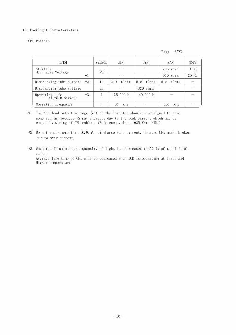
13. Backlight Characteristics
CFL ratings
Temp.= 25ѵ
ITEM SYMBOL MIN. TYP. MAX. NOTE
Starting ҥ ҥ 795 Vrms. 0 ѵdischarge Voltage VS
*1 ҥ ҥ 530 Vrms. 25 ѵ
Discharging tube current *2 IL 2.0 mArms. 5.0 mArms. 6.0 mArms. ҥ
Discharging tube voltage VL ҥ 320 Vrms. ҥ ҥ
Operating life *3 T 25,000 h 40,000 h ҥ ҥ(IL=5.0 mArms.)
Operating frequency F 30 kHz ҥ 100 kHz ҥ
*1 The Non-load output voltage (VS) of the inverter should be designed to have
some margin, because VS may increase due to the leak current which may becaused by wiring of CFL cables. (Reference value: 1035 Vrms MIN.)
*2 Do not apply more than (6.0)mA discharge tube current. Because CFL maybe broken
due to over current.
*3 When the illuminance or quantity of light has decreased to 50 ҡ of the initial
value.Average life time of CFL will be decreased when LCD is operating at lower andHigher temperature.
- 17 -
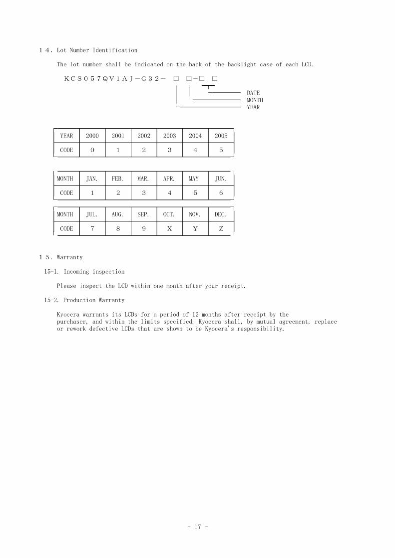
ɠɣϔLot Number Identification
The lot number shall be indicated on the back of the backlight case of each LCD.
ɳɫɻɟɤɦɹɾɠɩɲҥɯɢɡҥ Ӗ ӖҥӖ Ӗ
DATEMONTHYEAR
YEAR 2000 2001 2002 2003 2004 2005
CODE ɟ ɠ ɡ ɢ ɣ ɤ
MONTH JAN. FEB. MAR. APR. MAY JUN.
CODE ɠ ɡ ɢ ɣ ɤ ɥ
MONTH JUL. AUG. SEP. OCT. NOV. DEC.
CODE ɦ ɧ ɨ ʀ ʁ ʂ
ɠɤϔWarranty
15-1. Incoming inspection
Please inspect the LCD within one month after your receipt.
15-2. Production Warranty
Kyocera warrants its LCDs for a period of 12 months after receipt by thepurchaser, and within the limits specified. Kyocera shall, by mutual agreement, replaceor rework defective LCDs that are shown to be Kyocera's responsibility.
- 18 -
ɠɥϔPrecautions for use
16-1. Installation of the LCD
1. Please ground either of the mounting (screw) holes located at each corner of anLCD module, in order to stabilize brightness and display quality.
2. A transparent protection plate shall be added to protect the LCD and its polarizers.
3. The LCD shall be installed so that there is no pressure on the LSI chips.
4. The LCD shall be installed flat, without twisting or bending.
5. The display window size should be the same as the effective viewing area.
6. In case you use outside frame of effective viewing area as outward appearance ofyour product, unevenness of its outward appearance is out of guarantee.
7. Do not pull the CFL lead wires and do not bend the root of the wires. Housingshould be designed to protect CFL lead wires from external stress.
16-2. Static Electricity
1. Since CMOS ICs are mounted directly onto the LCD glass, protection from staticelectricity is required. Operation should wear ground straps.
16-3. LCD Operation
1. The LCD shall be operated within the limits specified. Operation at values outsideof these limits may shorten life, and/or harm display images.
2. Vop must be adjusted to optimize viewing angle and contrast.
3. Operation of the LCD at temperature below the limit specified may cause imagedegradation and/or bubbles. It may also change the characteristics of the liquidcrystal. This phenomenon may not recover. The LCD shall be operated within thetemperature limits specified.
16-4. Storage
1. The LCD shall be stored within the temperature and humidity limits specified.Store in a dark area, and protected the LCD from direct sunlight or fluorescentlight.
2. The LCD should be packaged to prevent damage.
- 19 -
16-5. Screen Surface
1. DO NOT store in a high humidity environment for extended periods. Imagedegradation, bubbles, and/or peeling off of polarizer may result.
2. The front polarizer is easily scratched or damaged. Prevent touching itwith any hard material, and from being pushed or rubbed.
3. The LCD screen may be cleaned with a soft cloth or cotton pad. Methanol, orIsopropyl Alcohol may be used, but insure that all solvent residue is removed.
4. Water may cause damage or discoloration of the polarizer. Clean any condensationor moisture from any source immediately.
5. Always keep the LCD free from condensation during testing. Condensation maypermanently spot or stain the polarizers.
- 20 -
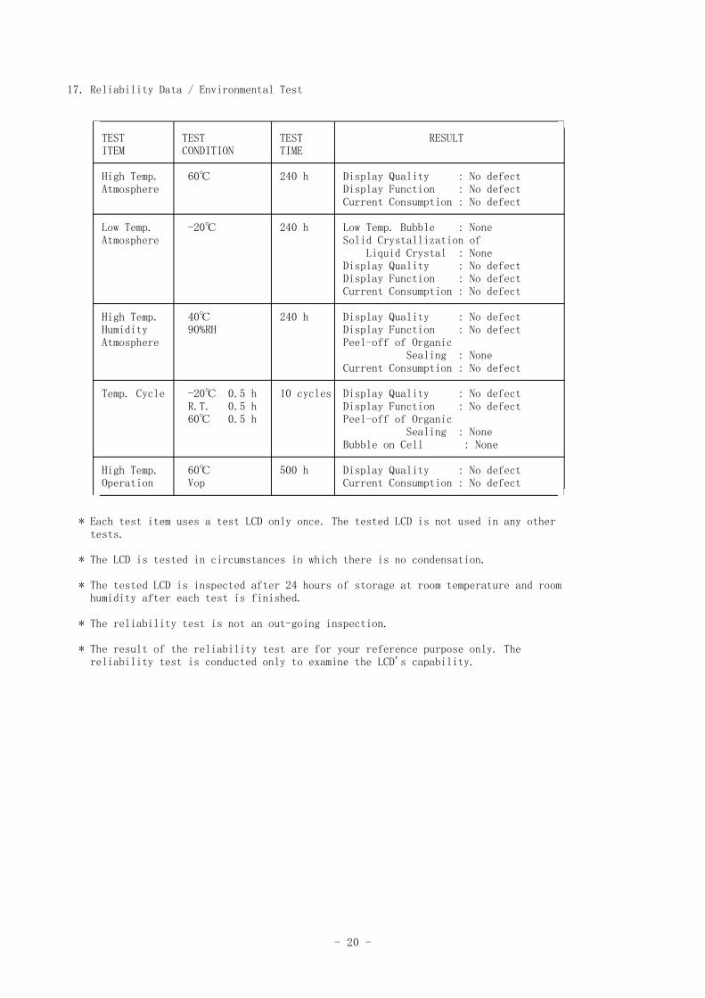
17ϔReliability Data / Environmental Test
TEST TEST TEST RESULTITEM CONDITION TIME
High Temp. 60ѵ 240 h Display Quality : No defectAtmosphere Display Function : No defect
Current Consumption : No defect
Low Temp. -20ѵ 240 h Low Temp. Bubble : NoneAtmosphere Solid Crystallization of
Liquid Crystal : NoneDisplay Quality : No defectDisplay Function : No defectCurrent Consumption : No defect
High Temp. 40ѵ 240 h Display Quality : No defectHumidity 90%RH Display Function : No defectAtmosphere Peel-off of Organic
Sealing : NoneCurrent Consumption : No defect
Temp. Cycle -20ѵ 0.5 h 10 cycles Display Quality : No defectR.T. 0.5 h Display Function : No defect60ѵ 0.5 h Peel-off of Organic
Sealing : NoneBubble on Cell : None
High Temp. 60ѵ 500 h Display Quality : No defectOperation Vop Current Consumption : No defect
* Each test item uses a test LCD only once. The tested LCD is not used in any othertests.
* The LCD is tested in circumstances in which there is no condensation.
* The tested LCD is inspected after 24 hours of storage at room temperature and roomhumidity after each test is finished.
* The reliability test is not an out-going inspection.
* The result of the reliability test are for your reference purpose only. Thereliability test is conducted only to examine the LCD's capability.


Revision Record
Designed by : Engineering Dept. Confirmed by : QA Dept.Date
Prepared Checked Approved Checked Approved
Rev. No. Date Page Descriptions
- 1 -
Visuals specification
1)Note
Item Note
General
1. When defects specified in this Inspection Standards are
inspected, operating voltage(Vop) shall be set at the
level where optimized contrast is available.
Display quality is applied up to effective viewing area.
(Bi-Level INSPECTION)
2. This inspection standard about the image quality shall be
applied to any defect within the effective viewing area
and shall not be applicable to outside of the area.
3. Should any defects which are not specified in this
standard happen, additional standard shall be determined
by mutual agreement between customer and Kyocera.
4. Inspection conditions
Luminance : 500 Lux minimum .
Inspection distance : 300 mm (from the sample)
Temperature : 25 r 5
Direction : right above
Definition of Inspection Pinhole, Bright spot The color of a small area is
item Black spot, Scratch different from the remainder.
Foreign particle The phenomenon dose not change
with voltage.
Contrast variation The color of a small area is
different from the remainder.
The phenomenon changes with
voltage.
Polarizer (Scratch, Scratch, Bubble and Dent in the
Bubble, Dent) polarizer which can be observed
in on / off state.

- 2 -
2)Standard
Inspection item Judgement standard
Pinhole, Bright spotBlack spot,Foreign particle
㨎
a
d = ( a + b ) / 2
Category Size (mm) Acceptable number
A d 0.2 neglected
B 0.2 㧨 d 0.3 5
C 0.3 㧨 d 0.5 3
D 0.5 㧨 d 0
Scratch, Foreign particle
W
L
Width (mm) Length (mm) Acceptable No.
A W 0.03 neglected
B L 2.0 neglected
C 0.03㧨 W 0.1 2.0 㧨 L 4.0 3
D 4.0 㧨 L 0
E 0.1 㧨 W According to' Circular '
Contrast variation
㨎
㨍d = ( a + b ) / 2
Category Size (mm) Acceptable number
A d 0.5 neglected
B 0.5 㧨 d 0.7 3
C 0.7 㧨 d 0

- 3 -
Inspection item Judgement standard
Polarizer (Scratch, (1) Scratch W
Bubble, Dent)
L
Width (mm) Length (mm) Acceptable No.
A W 0.1 neglected
B L 5.0 neglected
0.1 㧨 W 0.3
C 5.0 㧨 L 0
D 0.3 㧨 W 0
(2)Bubble ( dent )
㨎
㨍
d = ( a + b ) / 2
Category Size (mm) Acceptable number
A d 0.2 neglected
B 0.2 㧨 d 0.3 5
C 0.3 㧨 d 0.5 3
D 0.5 㧨 d 0