LAYOUT DATA IN TCAD FRAMEWORKS - TU · PDF fileLAYOUT DATA IN TCAD FRAMEWORKS ... ECAD...
5
LAYOUT DATA IN TCAD FRAMEWORKS R. Martins and S. Selberherr Institute for Microelectronics, TU Vienna Guf3hausstraf3e 27-29 A-1040 Vienna, Austria e-mail: [email protected].at ABSTRACT Today Technology CAD (TCAD) tools are essen- tial to the development of modern Integrated Cir- cuit (IC) fabrication processes. They are as well, required in the design/ optimization of very detailed and critical circuits related to a given IC process, where the usual higher level tools in Electronic De- sign CAD (ECAD) frameworks do not exhibit the precision or the features required. The boundary between TCAD and ECAD is not well established, and the interfacing between the two must be han- dled. This paper describes how ECAD and TCAD are linked inside the Viennese Integrated System for Technology CAD Applications (VISTA). 1 INTRODUCTION Enormous progress has been seen in the design au- tomation of very large integrated circuits, namely at the automatic synthesis and design verification levels. Most of this effort regarded digital inte- grated circuits, and very efficient tools to check the functional correctness of these designs were devel- oped [Pomeranz and Reddy 1993]. As the last generations of integrated circuits in- clude also analog sections (e.g. analog/digital con- verters), or very high performance circuits (e.g. ul- tra high clock speeds) which must be simulated at a detailed level, ECAD frameworks need new ca- pabilities to enable a correct analysis/optimization and verification of designs. Although TCAD frameworks are not intended to be used in the design of a complete integrated circuit, they include some features and tools that can be very useful, covering some lacks encountered in classical ECAD frameworks. In this paper we re- port on the concepts how these features are incor- porated in VISTA [S. Halama et al.1995] to achieve these objectives, and we give some examples. 2 LAYOUT IN VISTA FRAMEWORK As the final result of any ECAD framework is lay- out data, representing the mask artwork of the structures to be fabricated (or simulated), it is ob- vious that this information must be supplied to the TCAD framework. But in generality of such frame- works the tools used to display, print and interac- tively manipulate geometrical data, are a-priori not suitable to handle layout data. They were devel- oped mainly to edit device geometries (vertical de- sign) where there are no polygons overlapping. In addition instead of layer names, material types are defined. In VISTA data is stored in the Profile Inter- change Format (PIF) [F. Fasching et al.1994]. To the PIF EDitor [Rieger 1995] tool, that suffered from the above drawbacks, we added some func- tionality creating a special mode for layout editing. However, in most of the cases the better way is to use converters from CIF or GDS-II [Rubin 1987] layout representations to PIF. The PIF EDitor is used only for the visualization and manipulation
Transcript of LAYOUT DATA IN TCAD FRAMEWORKS - TU · PDF fileLAYOUT DATA IN TCAD FRAMEWORKS ... ECAD...

LAYOUT DATA IN TCAD FRAMEWORKS
R. Martins and S. Selberherr
Institute for Microelectronics, TU Vienna
Guf3hausstraf3e 27-29
A-1040 Vienna, Austria
e-mail: [email protected]
ABSTRACT
Today Technology CAD (TCAD) tools are essen
tial to the development of modern Integrated Cir
cuit (IC) fabrication processes. They are as well,
required in the design/ optimization of very detailed
and critical circuits related to a given IC process,
where the usual higher level tools in Electronic De
sign CAD (ECAD) frameworks do not exhibit the
precision or the features required. The boundary
between TCAD and ECAD is not well established,
and the interfacing between the two must be han
dled. This paper describes how ECAD and TCAD
are linked inside the Viennese Integrated System
for Technology CAD Applications (VISTA).
1 INTRODUCTION
Enormous progress has been seen in the design au
tomation of very large integrated circuits, namely
at the automatic synthesis and design verification
levels. Most of this effort regarded digital inte
grated circuits, and very efficient tools to check the
functional correctness of these designs were devel
oped [Pomeranz and Reddy 1993].
As the last generations of integrated circuits in
clude also analog sections (e.g. analog/digital con
verters), or very high performance circuits (e.g. ul
tra high clock speeds) which must be simulated at
a detailed level, ECAD frameworks need new ca
pabilities to enable a correct analysis/optimization
and verification of designs.
Although TCAD frameworks are not intended
to be used in the design of a complete integrated
circuit, they include some features and tools that
can be very useful, covering some lacks encountered
in classical ECAD frameworks. In this paper we re
port on the concepts how these features are incor
porated in VISTA [S. Halama et al.1995] to achieve
these objectives, and we give some examples.
2 LAYOUT IN VISTA FRAMEWORK
As the final result of any ECAD framework is lay
out data, representing the mask artwork of the
structures to be fabricated (or simulated), it is ob
vious that this information must be supplied to the
TCAD framework. But in generality of such frame
works the tools used to display, print and interac
tively manipulate geometrical data, are a-priori not
suitable to handle layout data. They were devel
oped mainly to edit device geometries (vertical de
sign) where there are no polygons overlapping. In
addition instead of layer names, material types are
defined.
In VISTA data is stored in the Profile Inter
change Format (PIF) [F. Fasching et al.1994]. To
the PIF EDitor [Rieger 1995] tool, that suffered
from the above drawbacks, we added some func
tionality creating a special mode for layout editing.
However, in most of the cases the better way is to
use converters from CIF or GDS-II [Rubin 1987]
layout representations to PIF. The PIF EDitor is
used only for the visualization and manipulation

!!!!J~~~~~~~~ : -13 -10 -:s 10
38
"' "' 30 ... "" ,. Z2
zo
•• '" ,. 1Z
10
q
-z -4
.....
..... -10
fllt!: leatZ~c;R pbf lJOOl'l"t 111H-~
Logical: loglcll.l1 Scop11 : layout
Figure 1: Displaying an imported piece of layout:
A CMOS inverter.
of this data. As the cited formats are extensively
used, the interface with any ECAD framework
is assured. In Figure 1. we present an inverter lay
out imported from the CADENCE DWF-II frame
work.
In general, the simulators inside TCAD frame
works can not handle large pieces of layout. There
fore a tool to interactively select areas of interest
from large layouts was created. In addition tools
to perform boolean operations with masks and to
filter/select given mask names were developed. An
overview diagram is shown in Figure 2.
Since most process and device simulators are
designed for two-dimensional applications, there is
the need to interactively specify the locations where
in the layout, a cut is to be performed. That means
the end points of the cut-line, as shown in Figure
3. have to be given. The tool designed for this task
can also warn the user of some problems associated
with this operation.
An interesting feature is that the result of the
ECAD VISTA
~ h> LAYOUT DATA (in PIF)
~ Area Boolean
Select Operations
Cut-line Select/Filter
Definition Mask Names
' 1 'v u ' v
INTERFACE PRINT DISPLAY
with SFC Data Data
Figure 2: Layout data in VISTA - Block diagram.
cut-line tool is understood by the VISTA Simu
lation Flow Controller(SFC) [Pichler 1993] so the
process simulation (and consequent device simula
tion) can be carried without the user have to explic
itly define etches using the absolute coordinates.
The interface relies in a LISP-like syntax format J
to make it easily compatible with the SFC code '
that it is implemented in LISP. In this way it is
also very flexible and easy to extend with new fea
tures, as required by the integration of the various
process and device simulators. Anyhow, in PIF the
layout data is stored in such a way, that these simu
lators can use it as stand-alone applications directly
without having to perform any further operations.
Another feature is the capability to understand
mask names. The mask names in the CIF file '
or in the technology file accompanying the GDS-
II files change between different technologies ( eg.
the metall layer can be "METALl" or sometimes
"METAL_l"). So some intelligence was added in
such a way that the user can select the desired layer
without knowing exactly its name, which of course
works only with the usual layers in IC technologies.

0 .. r i gina. .tyou t D t a a.
C u t- I i "le E d it
- -" Cut-line
/ '
' " -meta11
' -meto12 -metal1 -rnetal2
- -
Figure 3: Handling layout to perform a capacitance extraction.
3 EXAMPLES
In this section we present some examples how the
layout data can be used in TCAD. These are repre
sentative examples of typical simulation cases found
in critical integrated circuit design.
Figure 3. shows an example of how VISTA
can be used to extract accurate interconnect wire
..,. '
Potential
- 12 -9 -6 - 3 0 x I um
l2
>l. 0
0.9
0. 8
0. 7
0 . 6
o. 5
0. 4
0 . 3
0. 2
0 . 1
<0 . 0
Figure 4: Cut showing potential distribution in
wires.
capacitances. The layout was imported from a
commercial IC design framework that could not
calculate the capacitances between the conductors
in METAL2. First, a piece of layout (where one di
mension is not changing) was selected and then, a
cut performed. The result is then fed to the capac
itance extractor simulator SCAP [M. Mukai 1995].
Although SCAP has three-dimensional capabili
ties, in this example they are not used.
The result of the cut and the potential distri
bution in the wires are displayed in Figure 4. It
is to remark that a ground plane (the substrate)
is always assumed to exist and the material sur
rounding the wires is Si02. In the simulation,
the METALl conductor is at 1 V potential and all
the other conductors (substrate included) at a null
potential. In this situation the calculated capaci
tances are as in Table 1.
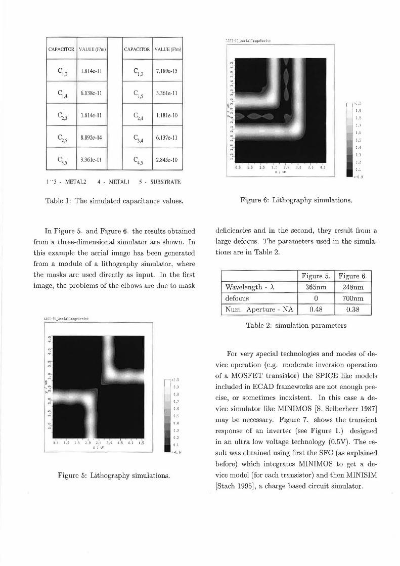
CAPACITOR VALUE(F/m) CAPACITOR VALUE(F/m)
c1.2 l.814e-l I c1 3 7.189e-15
c,,4 6.138e-11 c1 s 3.36le-l I
c2,3 l.814e-ll c2.4 1.18le-!O
c2,s 8.892e-14 c3.4 6.137e-l I
c3,s 3.361e-11 c4.s 2.845e-IO
I "3 - METAL2 4 - METAL! 5 - SUBSTRATE
Table 1: The simulated capacitance values.
In Figure 5. and Figure 6. the results obtained
from a three-dimensional simulator are shown. In
this example the aerial image has been generated
from a module of a lithography simulator, where
the masks are used directly as input . In the first
image, the problems of the elbows are due to mask
LISI -JD_AeriallmageResis t
... ..
2.0 2.5 3.0 x I um
n>l.O
0.9
0.8
0.7
0.6
0. 5
0.4
0.3
0.2
0.1
<-0.0
Figure 5: Lithography simulations.
LISI -3 D_Aerial ImageResist
G.5 l.G l.S 2.0 3.0 3.5 4.0 x I um
n>t.O
0.9
0.8
0. 7
0,6
0.5
0.4
0.3
0.2
0.1
<-0 .0
Figure 6: Lithography simulations.
deficiencies and in the second, they result from a
large defocus. The parameters used in the simula
tions are in Table 2.
Figure 5. Figure 6.
Wavelength - >. 365nm 248nm
defocus 0 700nm
Num. Aperture - NA 0.48 0.38
Table 2: simulation parameters
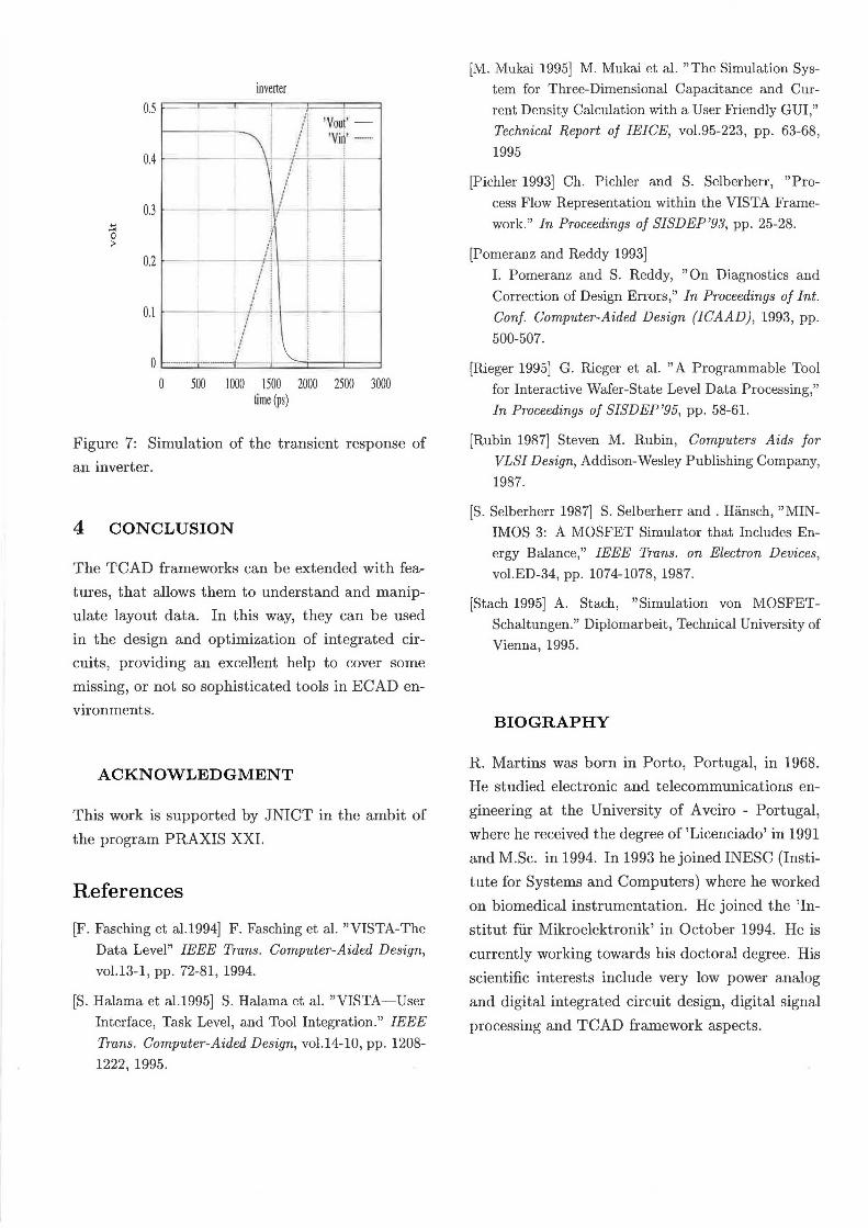
For very special technologies and modes of de
vice operation (e.g. moderate inversion operation
of a MOSFET transistor) the SPICE like models
included in ECAD frameworks are not enough pre
cise, or sometimes inexistent. In this case a de
vice simulator like MINIMOS [S. Selberherr 1987]
may be necessary. Figure 7. shows the transient
response of an inverter (see Figure 1.) designed
in an ultra low voltage t echnology (0.5V). The re
sult was obtained using first the SFC (as explained
before) which integrates MINIMOS to get a de
vice model (for each transistor) and then MINISIM
[Stach 1995], a charge based circuit simulator.
inverter 0.5 J:=:-=ic:=--=i:-----r-----,:::f = ::::::i::=::::i
j l 'V~~: = 0.4 .I
I -l l -+---+--1 l ' j
0.31----
A i l 0·2 1-~~--711-1
. I , ;
0.1 /-1-1-~ .i i I
0 -·-· ·--- _' - - !
0 500 I 000 1500 2000 2500 3000 time(ps)
Figure 7: Simulation of the transient response of
an inverter.
4 CONCLUSION
The TCAD frameworks can be extended with fea
tures, that allows them to understand and manip
ulate layout data. In this way, they can be used
in the design and optimization of integrated cir
cuits, providing an excellent help to cover some
missing, or not so sophisticated tools in ECAD en
vironments.
ACKNOWLEDGMENT
This work is supported by JNICT in the ambit of
the program PRAXIS XXL
References
[F. Fasching et al.1994] F. Fasching et al. "VISTA-The Data Level" IEEE Trans. Computer-Aided Design,
vol.13-1, pp. 72-81, 1994.
[S. Halama et al.1995] S. Halama et al. "VISTA- User Interface, Task Level, and Tool Integration." IEEE
Trans. Computer-Aided Design, vol.14-10, pp. 1208-
1222, 1995.
[M. Mukai 1995] M. Mukai et al. "The Simulation System for Three-Dimensional Capacitance and Current Density Calculation with a User Friendly GUI," Technical Report of IEICE, vol.95-223, pp. 63-68,
1995
[Pichler 1993] Ch. Pichler and S. Selberherr, "Pro
cess Flow Representation within the VISTA Framework." In Proceedings of SISDEP'93, pp. 25-28.
[Pomeranz and Reddy 1993] I. Pomeranz and S. Reddy, "On Diagnostics and Correction of Design Errors," In Proceedings of Int.
Conj. Computer-Aided Design (ICAAD), 1993, pp.
500-507 .
[Rieger 1995] G. Rieger et al. "A Programmable Tool for Interactive Wafer-State Level Data Processing," In Proceedings of SISDEP'95, pp. 58-61.
[Rubin 1987] Steven M. Rubin, Computers Aids for
VLSI Design, Addison-Wesley Publishing Company, 1987.
[S. Selberherr 1987] S. Selberherr and . Hansch, "MINIMOS 3: A MOSFET Simulator that Includes Energy Balance," IEEE Trans. on Electron Devices,
vol.ED-34, pp. 1074-1078, 1987.
[Stach 1995] A. Stach, "Simulation von MOSFETSchaltungen." Diplomarbeit, Technical University of Vienna, 1995.
BIOGRAPHY
R. Martins was born in Porto, Portugal, in 1968.
He studied electronic and telecommunications en
gineering at the University of Aveiro - Portugal,
where he received the degree of 'Licenciado' in 1991
and M.Sc. in 1994. In 1993 he joined INESC (Insti
tute for Systems and Computers) where he worked
on biomedical instrumentation. He joined the 'In
stitut fiir Mikroelektronik' in October 1994. He is
currently working towards his doctoral degree. His
scientific interests include very low power analog
and digital integrated circuit design, digital signal
processing and TCAD framework aspects.