LatticeXP2 Brevia Development Kit - Digi-Keymedia.digikey.com/PDF/Data Sheets/Lattice...
25
June 2010 Revision: EB53_01.1 LatticeXP2 Brevia Development Kit User’s Guide
Transcript of LatticeXP2 Brevia Development Kit - Digi-Keymedia.digikey.com/PDF/Data Sheets/Lattice...

June 2010Revision: EB53_01.1
LatticeXP2 Brevia Development Kit
User’s Guide

2
LatticeXP2 Brevia Development KitLattice Semiconductor User’s Guide
IntroductionThank you for choosing the Lattice Semiconductor LatticeXP2™ Brevia Development Kit!
This user’s guide describes how to start using the LatticeXP2 Brevia Development Kit, an easy-to-use platform for evaluating and designing with LatticeXP2 FPGAs. Along with the evaluation board and accessories, this kit includes a pre-loaded Brevia System-on-Chip (SoC) demonstration design based on the LatticeMico8™ microcon-troller.
Note: Static electricity can severely shorten the life span of electronic components.
FeaturesThe LatticeXP2 Brevia Development Kit includes:
• LatticeXP2 Brevia Evaluation Board – This is a small board (about the size of a business card) with the follow-ing on-board components and circuits:
– LatticeXP2-5E 6TN144C– 2-Mbit SPI Flash memory– 128K by 8-bit SRAM– RS232 DB9 connector– 2x20 expansion header for general I/O– 2x5 expansion header for general I/O– Four general purpose pushbuttons– One reset pushbutton– 4-bit DIP switch – Eight status LEDs
• Pre-loaded Demo – The kit includes a pre-loaded demo design that integrates several Lattice reference designs including the LatticeMico8 microcontroller, SRAM controller, SPI Flash memory controller, and a UART periph-eral.
• One RS232 DB9
• One Parallel Port Download Cable – The parallel port download cable permits reconfiguration of the FPGA. It also permits the use of the Reveal™ analysis tool. See Table 10 on page 17 for connection information.
• One International 6V DC Power Supply
• QuickSTART Guide – Provides information on connecting the LatticeXP2 Brevia Evaluation Board and running the demo.
• LatticeXP2 Brevia Development Kit Web Page — The LatticeXP2 Brevia Development Kit web page on the Lattice web site provides access to the latest documentation, demo designs and drivers for the kit.
The contents of this user’s guide include demo operation, top-level functional descriptions of the various portions of the evaluation board, descriptions of the on-board connectors, switches and a complete set of schematics of the LatticeXP2 Brevia Evaluation Board.

3
LatticeXP2 Brevia Development KitLattice Semiconductor User’s Guide
Figure 1. LatticeXP2 Brevia Evaluation Board, Top Side
RS232
PowerLED
PowerConnector
3.5”
2”
2.5V Expansion Header
JTAG Header20x20 Expansion Header
StatusLEDs
PushButtons
DIPSwitches
RESETButton
LatticeXP2 DeviceThis board features a LatticeXP2 FPGA with a 1.2V core supply. It can accommodate all pin-compatible LatticeXP2 devices in the 144-pin TQFP (20x20 mm) package. A complete description of this device can be found in the LatticeXP2 Family Data Sheet.
Demonstration DesignLattice provides a demo that illustrates key applications of the LatticeXP2 device.
Demo_LatticeXP2_Brevia_SoCThe Demo_LatticeXP2_Brevia_SoC is pre-programmed into the non-volatile Flash memory of the LatticeXP2 FPGA and is operational upon power-up. The design provides the following features:
• Prints the ASCII representation of any characters received by the UART on the eight LEDS (D0-D7).
• Prints the SPI memory ID code on demand.
• Displays the current DIP switch setting on demand.
• Logs Read ID and Read Switch commands, along with their results, into the asynchronous SRAM.
• Stores the contents of the SRAM into the SPI ROM on demand.
• Restores the SRAM contents from the SPI ROM on demand.

4
LatticeXP2 Brevia Development KitLattice Semiconductor User’s Guide
The demo design integrates the following Lattice reference designs:
• LatticeMico8 Microcontroller (RD1026)
• WISHBONE UART (RD1042)
• SPI WISHBONE Controller (RD1044)
• LatticeMico8 to WISHBONE Interface Adapter (RD1043)
Firmware running on the LatticeMico8 demonstrates control logic for the peripherals connected to a shared on-chip WISHBONE bus and communication between the LatticeXP2 Brevia Evaluation Board and a host PC connected to the RS232 cable.
Figure 2. Demo_LatticeXP2_Brevia_SoC Block Diagram
LatticeXP2 Brevia Evaluation Board
LED Bank
UART
SPI SRAM
RS-232PC Host
SPI MemoryController
SRAM MemoryController
SPI 2-MbitFlash Memory
SRAM 1-MbitMemory
LatticeMico8
WISHBONE Bus
Switch Bank
LatticeXP2 FPGA
Set Up a VT100/ANSI Terminal EmulatorThe Demo_LatticeXP2_Brevia_SoC preloaded in the LatticeXP2 Brevia Evaluation Board is operated by interact-ing with a monitor program. The monitor program sends and receives data across the RS232 communications port on the LatticeXP2 Brevia Evaluation Board. It is necessary to start and configure a VT100 or ANSI style terminal emulator program like HyperTerminal (Windows) or Minicom (Linux).
The RS232 port on the LatticeXP2 Brevia Evaluation Board is configured to operate at 115.2Kbps, 8 data bits, 1 stop bit, and no parity, and no flow control. Once the terminal emulator is running on the host computer, and the RS232 cable is attached between the host computer and the LatticeXP2 Brevia Evaluation Board you will see the following banner displayed when the board is powered, or following a RESET button assertion.
5
LatticeXP2 Brevia Development KitLattice Semiconductor User’s Guide
=========================================================================
Welcome to the LatticeXP2 Brevia Development KitSoC Demonstration Rev 1.0, April 2010
Main Menu------------------------------------------------------------ 0: Re-display Main Menu 1: Read SPI Flash Memory IDCode 2: Read DIP Switch Bank 3: Read Data History from SRAM 4: Copy Data History from SRAM to SPI Flash Memory 5: Read Data History from SPI Flash Memory 6: Write Data to SRAM (Specified Address and Data) 7: Read Data from SRAM (Specified Address) 8: Write Data to SPI (Specified Address and Data) 9: Read Data from SPI (Specified Address) a: SRAM Auto-Test b: SPI Auto-Test
Press 0-b to select an option.=========================================================================
SoC Command Monitor FeaturesThe LatticeXP2 Brevia Evaluation Board, after it powers up or is reset, begins running a command interpreter mon-itor under the control of the LatticeMico8 microcontroller. The monitor code waits for a keypress and immediately performs the requested function.
When the Read ID and Read Switch Bank commands are executed the ASCII output from the command is stored into the SRAM. The LatticeMico8 stores the next address to write in three of its general purpose registers. After power up the registers are cleared to 0x000000. Commands that have their results logged to the SRAM print out the address of the next available SRAM location.
Read SPI Flash Memory IDCode CommandThe SPI ROM device on the LatticeXP2 Brevia Evaluation Board can be queried and will return the ID code imple-mented by the ROM manufacturer. The LatticeMico8 initiates memory transactions using the SPI Memory control-ler to acquire the data.
To scan the SPI Flash Memory IDCode:
1. From the terminal Main Menu, press 1.
The LatticeMico8 performs the manufacturer specific SPI memory transactions to acquire the ID code. The ID number is returned as a hex value. This command logs the result to the SRAM.
Example:
ID:0x44 (SRAM ADDR:0x00006)
Note: The ID for your board may differ.

6
LatticeXP2 Brevia Development KitLattice Semiconductor User’s Guide
Read DIP Switch BankThe LatticeMico8 has the ability to read the state of switches 1-4 on the DIP switch bank. The pushbutton switches are can also be read. Each pushbutton press toggles the internal state of a register in the FPGA. The current state of the register is displayed on the high nibble of the output. The hexadecimal representation of the switches is printed and logged to the SRAM. A DIP switch that is set ON has a '0' value, and one that is OFF has a value of '1'.
To read the DIP switch:
1. From the terminal window press 2.
Example:
SW:0x00 (SRAM ADDR:0x0000C)
Read Data History from SRAMUse the Read Data History from SRAM command to see the results from each command that is logged to the SRAM memory. The output from this command does not get written into the SRAM.
To read data history from SRAM:
1. From the terminal window press 3. The transaction log is listed.
Example:
SRAM: 0x44 0x00
Copy Data History from SRAM to SPI Flash MemoryThis command erases a portion of the SPI ROM, and stores the command results logged in the SRAM. The LatticeMico8 starts writing from SRAM address 0x000000 and continues writing values into the SPI ROM until it reaches the last valid entry in the SRAM.
To copy data history from SRAM to SPI Flash memory:
1. From the terminal window press 4. The data log is transferred and the terminal indicates “Done”.
Example:
SRAM => SPI: 0x44 0x00Done.

7
LatticeXP2 Brevia Development KitLattice Semiconductor User’s Guide
Read Data History From SPI Flash MemoryThis command copies the Data History from the SPI ROM into the SRAM. After power is supplied, or RESET asserted the SRAM Data History log information is no longer available. Running this command permits the history to be restored from the non-volatile SPI ROM.
To read data history from the SPI ROM into SRAM:
1. From the terminal window press 5. The transaction log is listed.
Example:
SPI Flash: 0x44 0x00
Write Data to SRAM (Specified Address and Data)This command allows you to write a single data value to any location in the SRAM memory space.
1. From the terminal window press 6.Example:Please Enter the Address(17 bits,Hex), eg: 1f26a, no Spaces, then Press ENTER:10000Please Enter the Data(8 bits,Hex), eg: b7, no Spaces, then Press ENTER:93SRAM Write Done.
Read Data from SRAM (Specified Address)This command allows you to read the data value from any address in the SRAM.
1. From the terminal window press 7.Example:Please Enter the Address(17 bits,Hex), eg: 1f26a, no Spaces, then Press ENTER:10000Read Data: 93SRAM Read Done.
Write Data to SPI (Specified Address and Data)This command allows you to write a single data value to any location in the SPI memory space.
1. From the terminal window press 8.Example:Please Enter the Address(18 bits,Hex), eg: 1f26a, no Spaces, then Press ENTER:10000Please Enter the Data(8 bits,Hex), eg: b7, no Spaces, then Press ENTER:93SPI Write Done.
8
LatticeXP2 Brevia Development KitLattice Semiconductor User’s Guide
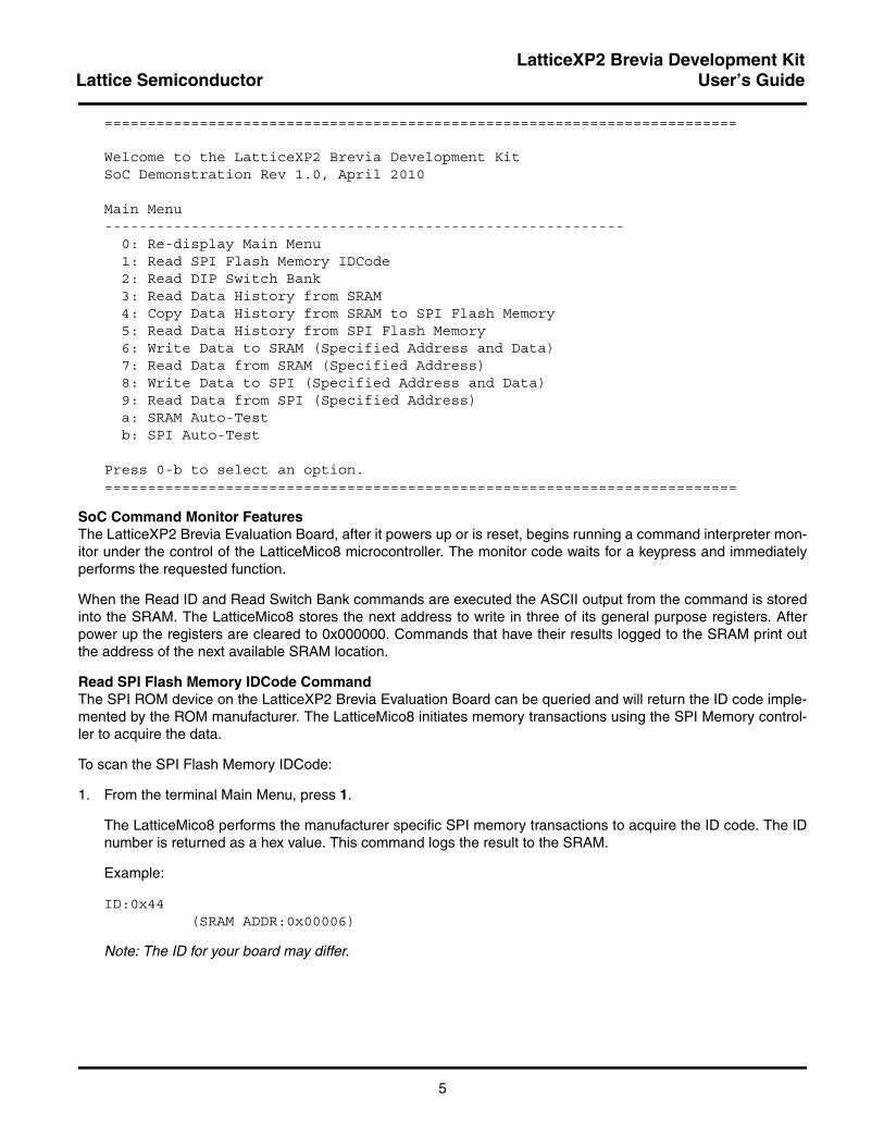
Read Data from SPI (Specified Address)This command allows you to read the data value from any address in the SPI.
1. From the terminal window press 9.Example:Please Enter the Address(18 bits,Hex), eg: 1f26a, no Spaces, then Press ENTER:10000Read Data: 93SPI Read Done.
Perform SRAM Auto-testThis command automatically tests SRAM.
1. From the terminal window press a.Example:> aStarting SRAM Auto-Test................................................................................................................................SRAM Test Done: Successful.
Perform SPI Auto-testThis command automatically tests SPI.
1. From the terminal window press b.Example:>bStarting SPI Auto-Test................................................................................................................................SPI Test Done: Successful.
Download Demo DesignsLattice distributes source and programming files for a variety of demonstration designs compatible with the LatticeXP2 Brevia Evaluation Board.
To download demo designs:
1. Browse to the LatticeXP2 Brevia Development Kit web page of the Lattice web site. Select the Demo Applica-tions download and save the file.

9
LatticeXP2 Brevia Development KitLattice Semiconductor User’s Guide
2. Extract the contents of Demo_LatticeXP2_Brevia_Soc_vhdl.zip and Demo_LatticeXP2_Brevia_Soc_verilog.zip to an accessible location on your hard drive. One or more designs will be extracted and each will follow the following basic form.
Demo Directories
Demo1 Demo1 .\project .\source .\LatticeMico8_Vx_y_Verilog .\RD1042 .\project .\source .\RD1043 .\project .\source .\RD1044 .\project .\source .\RD1046 .\project .\source
Where:
• \project – ispLEVER project (.syn), preferences (.lpf), and programming file (.jed). This directory may contain intermediate results of the ispLEVER build process.
• \source – HDL source for the ispLEVER project.
• .\LatticeMico8_Vx_y_Verilog – LatticeMico8 Microcontroller Reference Design (RD1026).
• .\RDxxxx – Reference Designs integrated by the demo.
10
LatticeXP2 Brevia Development KitLattice Semiconductor User’s Guide
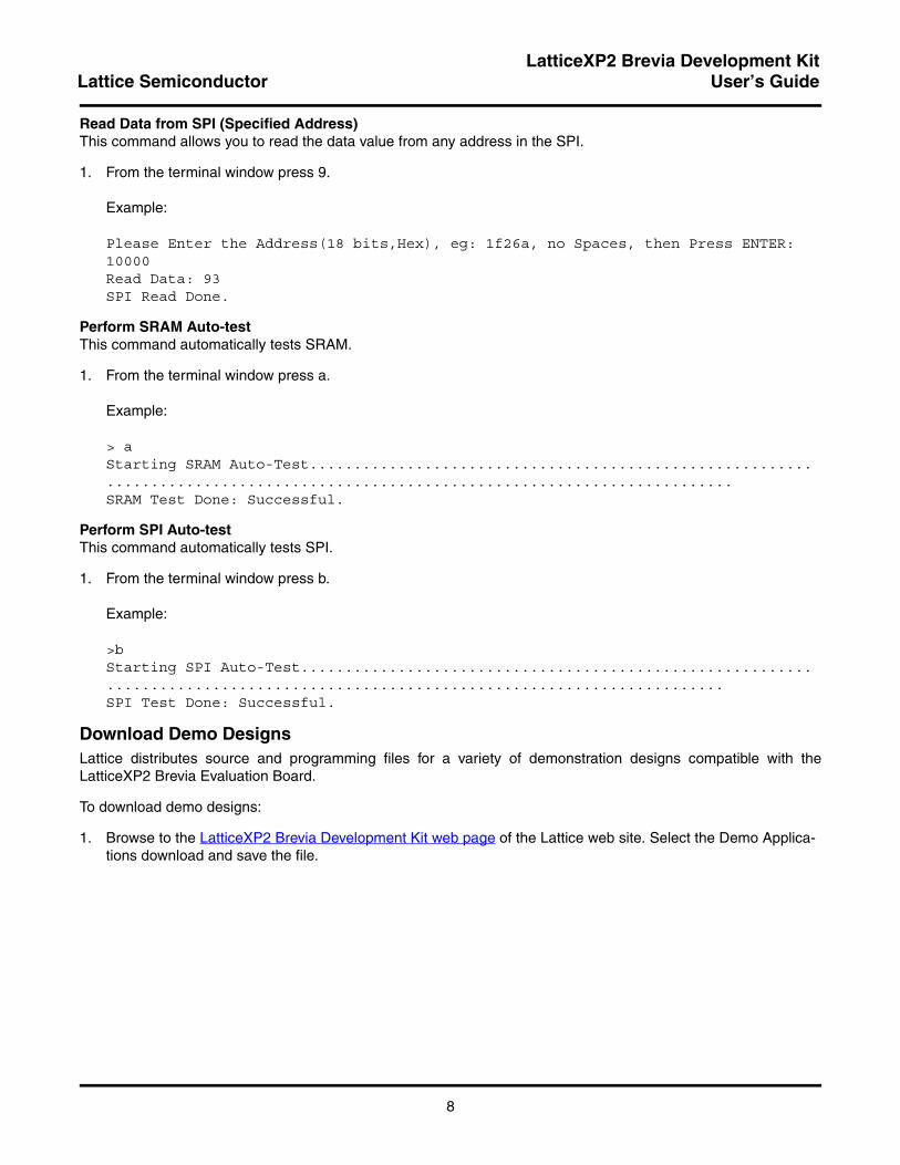
Programming Demo Design with ispVMDemo_LatticeXP2_Brevia_SoC is pre-programmed into the LatticeXP2 Brevia Evaluation Board by Lattice. To restore a LatticeXP2 Brevia Evaluation Board to factory settings, use the procedure described in this section.
To program a demo programming file:
1. Power off the LatticeXP2 Brevia Evaluation Board.
2. Connect the Parallel Port download cable to the PC
3. Connect opposite end of the Parallel Port download cable as shown in Table 9, leaving Pin 2 unconnected.
4. Apply power to the LatticeXP2 Brevia Evaluation Board.
5. Attach the download cable to Pin 2.
6. From the Start menu run ispVM System.
7. Choose Options > Cable and IO Port Setup... in order to configure the download cable.
8. Click Auto Detect. ispVM will detect Cable Type Lattice and Port Setting 0x0378.
9. Click OK.
10. Choose ispTools > Scan Chain. The New Scan Configuration Setup window appears. The LatticeXP2 appears in the device list as LFXP2-5E.
11. Right-click the LFXP2-5E entry and choose Edit Device... The Device Information dialog appears.
12. From the Data File section, click the Browse button. The Open Data File dialog appears.

11
LatticeXP2 Brevia Development KitLattice Semiconductor User’s Guide
13. Browse to the <Demo Dir>\project folder, select <Demo>.jed, and click Open. From the Operation list choose Flash Erase, Program, Verify and click OK.
14. Choose Project > Download. ispVM reprograms the LatticeXP2 Brevia Evaluation Board.
A progress bar with a small timer window will appear to show elapsed programming time. At the end of pro-gramming, the configuration setup window’s “Status” column will display “PASS” upon a successful program-ming sequence.
Rebuilding the Demo Project with ispLEVERYou can rebuild the Lattice-supplied demo. Follow the process outlined here:
1. Install and license ispLEVER software
2. Install the ispVM System software. The ispVM System software is bundled with ispLEVER, so this step is typi-cally unnecessary to perform independently.
3. Download the demo source files from the LatticeXP2 Brevia Development Kit web page.
4. Run the ispLEVER Project Navigator.
5. Use File -> Open Project and open the ispLEVER <demo>.syn.
6. Right-click on the Generate Data File (JEDEC) process and select Force.
7. Wait for the JED file to be rebuilt. Use ispVM System, as described above, to download the newly rebuilt bit-stream.

12
LatticeXP2 Brevia Development KitLattice Semiconductor User’s Guide
Reassembling the Demo LatticeMico8 FirmwareUse this procedure to reassemble and download changes to the LatticeMico8 microcontroller firmware.
1. Install the LatticeMico8 Tool Code.
Note: The LatticeMico8 tool executables are also provided in the . \Demo_LatticeXP2_Brevia_SoC\LatticeMico8_Vx_y_Verilog\utils directory and. \Demo_LatticeXP2_Brevia_SoC\LatticeMico8_Vx_y_VHDL\utils directory
2. The C source code for the LatticeMico8 Assembler and Simulator is included in the tools package.An optional step you can perform is to compile this source instead of using the pre-compiled versions supplied by Lattice.
3. Modify the Assembly source (.s) file, if desired, and recompile to a memory image (.hex). Source for Demo_LatticeXP2_Brevia_SoC is provided as Demo_LatticeXP2_Brevia_SoC.s. The assembler and simulator are command line applications. The tools display their invocation syntax if they are started without command line parameters.
4. Once the assembly code has been recompiled it is necessary to update the LatticeMico8 PROM contents. The fastest way to update the PROM contents is to use the ispLEVER Memory Initialization tool from Project Navi-gator. The tool updates the PROM contents without modifying the connectivity of the design.
Launch the Memory Initialization tool, and select the isp8_prom component, choose the new memory initializa-tion file, click on the Apply Changes button, and save the new NCD file.
5. Run the Generate Data File (JEDEC) process.
6. Download the new JED file to the FPGA. You will see the effects of your assembly code changes.
LatticeXP2 Brevia Evaluation BoardThis section describes the features of the LatticeXP2 Brevia Evaluation Board in detail.
OverviewThe LatticeXP2 Brevia Evaluation Board is a complete development platform for the LatticeXP2 FPGA. The board includes on-board SRAM and SPI Flash memory, and SPI microcontroller communication interfaces, a RS232 port, and an expansion header to support test connections.
Figure 3. LatticeXP2 Brevia Evaluation Board Block Diagram
LatticeXP2LFXP2-5E-6TN144C
2x20Header
2x5Header
2x5Header
SPI FlashSPI
1 MbitSRAM
Push-button (x4)
Push-button
8 LEDs
4-Bit DIP Switch
50 MHzCrystal
JTAGProgramming
28
4
8
31
DB9 RS232 Serial
SerialCommunication
8
4
GPIO
GSRN/IO

13
LatticeXP2 Brevia Development KitLattice Semiconductor User’s Guide
I/O Mapping DetailsUART InterfaceThe UART is used to communicate with the PC. U3 does the level translation between the LVCMOS I/Os and the RS232 port. The connector is a 9-pin D-type female. The interface details are included in Table 1.
Table 1. RS232 Interface
RS232 Connector
Pin Number
RS232 ConnectorPin Name
U3 Pin Number
to J1
U3 Pin Number
to U4FPGA
Pin NumberFPGA
Pin NamePin
Functionality
RS232 Connector J1A, Bank 1
1 NC NC NC NC NC NC
2 RS232_Rx_EIA32 13 12 110 RS232_Rx_TTL Receive
3 RS232_Tx_EIA32 14 11 109 RS232_Tx_TTL Transmit
4 NC NC NC NC NC NC
5 Ground Ground Ground Ground Ground Ground
6 NC NC NC NC NC NC
7 NC NC NC NC NC NC
8 NC NC NC NC NC NC
9 NC NC NC NC NC NC
Expansion Header 1 InterfaceAccess to 40 I/Os are available to the user via the expansion headers J2 and J4. The connector type is a 2x20 0.100" center-to-center Berg stick, male. The interface details are included in Table 2.
Table 2. Expansion Header 1 Interface
Expansion ConnectorPin Number
Expansion Connector/FPGAPin Name
FPGAPin Number Pin Functionality
Expansion Connector J4, Banks 2 and 3
1 3.3V Power
2 3.3V Power
3 EXP_IO15 103 I/O
4 EXP_IO31 69 I/O
5 EXP_IO14 102 I/O
6 EXP_IO30 66 I/O
7 EXP_IO13 101 I/O
8 EXP_IO29 65 I/O
9 EXP_IO12 100 I/O
10 EXP_IO28 62 I/O
11 EXP_IO11 99 I/O
12 EXP_IO27 61 I/O
13 GND Ground
14 GND Ground
15 EXP_IO10 98 I/O

14
LatticeXP2 Brevia Development KitLattice Semiconductor User’s Guide
Expansion Header 2 InterfaceThe connector is a 10-pin dual-row Berg stick, male. The interface details are included in Table .
Table 3.
Expansion ConnectorPin Number
Expansion Connector Pin Name
FPGA Pin Number Pin Functionality
Expansion Connector J2, Bank 2 and 3 (Labeled as J24 on Silk Screen)
1 EXP_IO36 31 I/O
2 3.3V Power
3 EXP_IO37 32
4 EXP_IO32 27
5 EXP_IO38 35
6 EXP_IO33 28
7 EXP_IO39 36
8 EXP_IO34 29
9 GND Ground
10 EXP_IO35 30
Expansion Header 2 Interface
Expansion Connector J4, Bank 2 and 3
16 EXP_IO26 116 I/O
17 EXP_IO9 96 I/O
18 EXP_IO25 115 I/O
19 EXP_IO8 94 I/O
20 EXP_IO24 114 I/O
21 EXP_IO7 93 I/O
22 EXP_IO23 113 I/O
23 EXP_IO6 92 I/O
24 EXP_IO22 78 I/O
25 GND Ground
26 GND Ground
27 EXP_IO5 91 I/O
28 EXP_IO21 77 I/O
29 EXP_IO4 90 I/O
30 EXP_IO20 74 I/O
31 EXP_IO3 89 I/O
32 EXP_IO19 73 I/O
33 EXP_IO2 88 I/O
34 EXP_IO18 108 I/O
35 EXP_IO1 87 I/O
36 EXP_IO17 107 I/O
37 GND Ground
38 GND Ground
39 XP2_RESET 19 Reset
40 EXP_IO16 104 I/O
Table 2. Expansion Header 1 Interface (Continued)
Expansion ConnectorPin Number
Expansion Connector/FPGAPin Name
FPGAPin Number Pin Functionality

15
LatticeXP2 Brevia Development KitLattice Semiconductor User’s Guide
LEDs and SwitchesEight LEDs, four pushbutton switches and one DIP (4) switch are provided.
Table 4.
LED FPGA Pin Number
D1 46
D2 45
D3 44
D4 43
D5 40
D6 39
D7 38
D8 37
LED Interface
Table 5.
Switch FPGA Pin Number
SW1A 58
SW1B 57
SW1C 56
SW1D 55
SW3 54
SW4 53
SW5 52
SW6 50
Switch Interface
Flash InterfaceThe LatticeXP2 Brevia Evaluation Board provides 4Mbits of non-volatile flash memory. The Flash uses the four-wire SPI communication interface.
Table 6.
Flash Signal Name FPGA Pin Number
FPGA Flash 2 Mbit (U1)
XP2_SPI_CS0 11
XP2_SPI_CLK 13
XP2_SPI_IN 15
XP2_SPI_OUT 16
FLASH_RST~ 17
FLASH_W~ 18
Flash Interface

16
LatticeXP2 Brevia Development KitLattice Semiconductor User’s Guide
SRAM InterfaceThe LatticeXP2 Brevia Evaluation Board provides 1Mbit of asynchronous SRAM memory in a 128K x 8-bit configu-ration.
Table 7.
SRAM Signal NameFPGA Pin Number
FPGA SRAM 1 Mbit (U2)
Data_0 1
Data_1 2
Data_2 5
Data_3 6
Data_4 7
Data_5 8
Data_6 9
Data_7 10
Addr_0 119
Addr_1 120
Addr_2 121
Addr_3 122
Addr_4 123
Addr_5 124
Addr_6 125
Addr_7 127
Addr_8 129
Addr_9 130
Addr_10 131
Addr_11 132
Addr_12 133
Addr_13 134
Addr_14 137
Addr_15 138
Addr_16 141
SRAM_CSb 142
SRAM_Oeb 143
SRAM_Web 144
SRAM Interface
Configuration InterfaceJumper 5 controls the XP2 CFG0 input control pin.
Table 8. Configuration Interface
CFG0Jumper Position
1 1-2
0 2-3
The factory default setting on J5 is to leave it unshunted. CFG0 has a weak pullup resistor.
17
LatticeXP2 Brevia Development KitLattice Semiconductor User’s Guide
Table 9. JTAG Programming Interface
JTAG ConnectorPin Number
JTAG ConnectorPin Name
FPGAPin Number
FPGAPin Name Pin Functionality
JTAG Connector J3
1 JTAG_TDO 82 JTAG_TDO TDO
2 3.3V — — VCC
3 JTAG_TDI 80 JTAG_TDI TDI
4 GND — — GND
5 JTAG_TMS 79 JTAG_TMS TMS
6 GND — — GND
7 JTAG_TCK 81 JTAG_TCK TCK
8 GND — — GND
9 GND — — GND
10 GND — — GND
FPGAThe Lattice XP2 Brevia board is based on the Lattice Semiconductor LatticeXP2 non-volatile FPGA. The board is populated with a 5K LUT device in a 144 TQFP package. A complete description of the device can be found in the LatticeXP2 Family Data Sheet and on the LatticeXP2 web page.
JTAG Cable Color Coding Table 10. JTAG Cable Color Coding
Color J3 Pin Number Association
Violet 1 TDO
Blue 2 VCC
Green 3 TDI
Yellow 4 GND
Orange 5 TMS
Red 6 GND
Brown 7 TCK
Black 8 GND
- 9 GND
- 10 GND
Software RequirementsYou should install the following software before you begin developing designs for the evaluation board:
• ispLEVER Starter or ispLEVER 7.2 SP2 or later
• ispVM System 17.3.3
Mechanical SpecificationsDimensions: 3-1/4 in. [L] x 2 in. [W] x 3/4 in. [H]
Environmental RequirementsThe evaluation board must be stored between -40° C and 100° C. The recommended operating temperature is between 0° C and 55° C.

18
LatticeXP2 Brevia Development KitLattice Semiconductor User’s Guide
The evaluation board can be damaged without proper anti-static handling.
GlossaryDIP: Dual In-line Package
FPGA: Field-Programmable Gate Array
LED: Light Emitting Diode
LUT: Look-Up Table
PCB: Printed Circuit Board
RoHS: Restriction of Hazardous Substances Directive
PLL: Phase Locked Loop
SPI: Serial Peripheral Interface
SRAM: Static Random Access Memory
UART: Universal Asynchronous Receiver/Transmitter
WDT: Watchdog Timer
TroubleshootingThe LatticeXP2 Brevia Evaluation Board is not responsive.
• Verify the DC power supply is providing 6V DC.
• Remove any jumper on J5.
• Verify the LatticeXP2 is programmed.
The functionality displayed by the board does not match the demo features described.It is possible the LatticeXP2 Brevia Evaluation Board has been reprogrammed. You can either reprogram the FPGA with the demonstration bitstream, or read the checksum of the bitstream loaded in the FPGA. To restore the LatticeXP2 Brevia Evaluation Board to the factory default, see the Download Demo Designs section of this docu-ment for details on downloading and reprogramming the device.
You can use ispVM System to read the checksum of the bitstream programmed into the FPGA. This value can be compared against the checksum stored in the JEDEC file. The JEDEC file checksum value is the last line in the file. This may allow you to determine the contents of the FPGA.
A final option is to use ispVM System to read the current bitstream in the FPGA, and then to reprogram the FPGA with your desired bitstream.
Ordering Information
Description Ordering Part NumberChina RoHS Environment-Friendly
Use Period (EFUP)
LatticeXP2 Brevia Development Kit LFXP2-5E-B-EVN

19
LatticeXP2 Brevia Development KitLattice Semiconductor User’s Guide
Technical Support AssistanceHotline: 1-800-LATTICE (North America)
+1-503-268-8001 (Outside North America)e-mail: [email protected]: www.latticesemi.com
Revision HistoryDate Version Change Summary
June 2010 01.0 Initial release.
June 2010 01.1 Updated zip file names in the “Download Demo Designs” text section.
Updated directory names in the “Reassembling the Demo LatticeMico8 Firmware” text section.
(c) 2010 Lattice Semiconductor Corp. All Lattice trademarks, registered trademarks, patents, and disclaimers are as listed at www.latticesemi.com/legal. All other brand or product names are trademarks or registered trademarks of their respective holders. The speci• cations and information herein are subject to change without notice.

20
LatticeXP2 Brevia Development KitLattice Semiconductor User’s Guide
Appendix A. SchematicsFigure 4. LatticeXP2 Brevia Evaluation Board Block Diagram
21
LatticeXP2 Brevia Development KitLattice Semiconductor User’s Guide
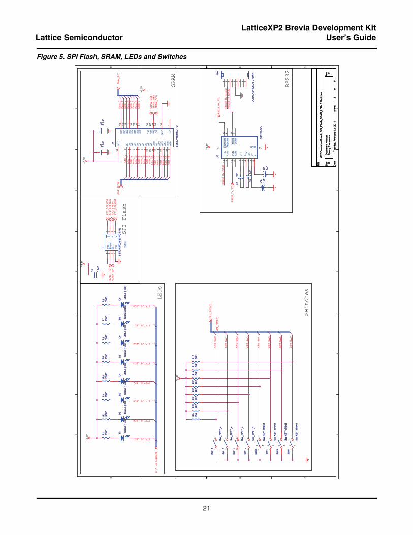
Figure 5. SPI Flash, SRAM, LEDs and Switches

22
LatticeXP2 Brevia Development KitLattice Semiconductor User’s Guide
Figure 6. Banks 6 and 7

23
LatticeXP2 Brevia Development KitLattice Semiconductor User’s Guide
Figure 7. Banks 0-5

24
LatticeXP2 Brevia Development KitLattice Semiconductor User’s Guide
Figure 8. Power

25
LatticeXP2 Brevia Development KitLattice Semiconductor User’s Guide
Appendix B. Bill of MaterialsTable 11. Bill of Materials
Item Quantity Reference Part PCB Footprint
1 19C1,C2,C3,C10,C11,C16,C17,C19,C20,C21,C23,C28,C29,C30,C31,C39,C40,C41,C42
0.1uF CC0402
2 6 C4,C5,C6,C7,C27,C38 1uF CC0402
3 1 C8 15pF CC0402
4 5 C9,C32,C43,C44,C45 0.01uF CC0402
5 6 C12,C13,C14,C15,C18,C22 10nF CC0402
6 4 C24,C26,C33,C37 10uF CC3528
7 2 C25,C34 100uF CC3528
8 8 D1,D2,D3,D4,D5,D6,D7,D8 Status (Green) LED0805
9 1 D10 Power ON (Red) LED0805
10 1 J1 CONN ASY DSUB 9-R/9-R CON_DSUBRT_9FM
11 2 J2,J3 CONN PCB 5x2 BERG_2X5
12 1 J4 CONN PCB 20x2 BERG_2X20
13 1 J5 JUMPER BERG_1X3
14 1 J6 PHONEJACK CON_DC006_PWRJACK
15 9 R1,R2,R3,R4,R5,R6,R7,R8,R30 330E RC0402
16 8 R9,R10,R11,R12,R13,R14,R15, R16 2k2 RC0402
17 1 R18 0 RC0402
18 3 R19,R25,R26 10K RC0402
19 2 R20,R22 0E RC0402
20 1 R21 121E RC0402
21 1 R23 240E RC0402
22 1 R24 390E RC0402
23 1 SW1 SW_SPST_4 SW_DIP8
24 4 SW3,SW4,SW5,SW6 SW KEY-YM061 SW_B3FS-1000P
25 1 S1 XP2 Reset SW_B3FS-1000P
26 1 U1 SST25VF020-20-4C-SAE SOIC127P600_8
27 1 U2 BS62LV1027SC-70 SOIC127P1400_32
28 1 U3 ST3232/SO SOIC127P780_16
29 1 U4 LFXP2-5E-T144/TN144 TQFP50P2200X2200_144
30 2 U5,U6 LM1117A SOT223
31 1 X1 3SWO50.00 7 X 5 crystal oscillator


![From Lattice Boltzmann Method to Lattice Boltzmann Flux … · From Lattice Boltzmann Method to Lattice Boltzmann Flux Solver Yan Wang 1, ... flows [8,13–15], compressible flows](https://static.fdocuments.us/doc/165x107/5cadf91b88c9938f4d8c0cd6/from-lattice-boltzmann-method-to-lattice-boltzmann-flux-from-lattice-boltzmann.jpg)