LABORATORY MANUAL - Weebly
46
CHENDU COLLEGE OF ENGINEERING AND TECHNOLOGY MADURANTAKAM. KANCHEEPURAM-603311. EC 6411 CIRCUITS AND SIMULATION INTEGRATED LABORATORY LABORATORY MANUAL Prepared by C.KRITHIKA, ASSISTANT PROFESSOR Faculty of Electronics & Communication Engineering Downloaded from www.Rejinpaul.com Get Unique study materials from www.rejinpaul.com
Transcript of LABORATORY MANUAL - Weebly

1
CHENDU
COLLEGE OF ENGINEERING AND TECHNOLOGY
MADURANTAKAM.
KANCHEEPURAM-603311.
EC 6411
CIRCUITS AND SIMULATION INTEGRATED
LABORATORY
LABORATORY MANUAL
Prepared by
C.KRITHIKA, ASSISTANT PROFESSOR
Faculty of Electronics & Communication Engineering
Downloaded from www.Rejinpaul.com
Get Unique study materials from www.rejinpaul.com

2
INDEX
EXPT.NO NAME OF THE EXPERIMENT PAGE NO
1 HALF WAVE AND FULL WAVE RECTIFIER
3
2 FIXED BIAS AMPLIFIER CIRCUIT USING BJT
9
3 BJT AMPLIFIER USING VOLTAGE DIVIDER BIAS
CE-CONFIGURATION
12
4 DIFFERENTIAL AMPLIFIER USING BJT 15
5 DARLINGTON AMPLIFIER USING BJT
18
6 SOURCE FOLLOWER WITH BOOTSTRAPPED CIRCUIT 21
7 CLASS - A POWER AMPLIFIER 24
8 CLASS – B COMPLEMENTARY SYMMETRY POWER
AMPLIFIER
27
9 FREQUENCY RESPONSE OF CE AMPLIFIER WITH EMITTER
RESISTANCE AMPLIFIER
32
10 DC RESPONSE OF CS AMPLIFIER
36
11 FREQUENCY RESPONSE OF CASCODE
AMPLIFIER
38
12 TRANSFER CHARACTERISTICS OF CLASS-B POWER
AMPLIFIER
40
13 DESIGN OF A DC POWER SUPPLY USING RECTIFIER
43
Downloaded from www.Rejinpaul.com
Get Unique study materials from www.rejinpaul.com

3
EXP.NO : 1 DATE:
HALF WAVE RECTIFIER:
AIM: To construct a half wave rectifier with simple capacitor filter and to measure its
ripple factor from the output waveforms.
APPARATUS REQUIRED:
S NO APPARATUS RANGE QUANTITY
1 RESISTOR 1K 1
2 CAPACITOR 470 μf 1
3 DIODE IN4007 1
4 STEP DOWN
TRANSFORMER
1
5 BREAD BOARD 1
6 CONNECTING
WIRES
FEW
7 CRO 1
CIRCUIT DIAGRAM:
Half wave rectifier with filter
HALF WAVE AND FULL WAVE RECTIFIER
Downloaded from www.Rejinpaul.com
Get Unique study materials from www.rejinpaul.com

4
MODEL GRAPH:
THEORY:
A Half wave rectifier is a device which converts ac voltage to pulsating dcvoltage using one
PN junction diode.The ac voltage (230 V, 50 HZ) is connected to the primary of the transformer.
Thetransformer steps down the ac voltage. Thus, with suitable turns ratio we get desired ac
secondary voltage. The rectifier circuit converts this ac voltage in to a pulsating dcvoltage. Half
wave rectifier conducts during positive half cycle and gives output in the form of positive
sinusoidal pulses. Hence the output is called pulsating dc. A pulsating dc voltage containing large
varying component called ripple in it. The capacitor filter is used after rectifier circuit, which
reduces the ripple content in the pulsating dc. Thus filter converts pulsating dc in to pure dc.
Ripple Factor:
The output of the rectifier is of pulsating dc type. The amount of ac content in theoutput can be
mathematically expressed by a factor called ripple factor.
Downloaded from www.Rejinpaul.com
Get Unique study materials from www.rejinpaul.com
5
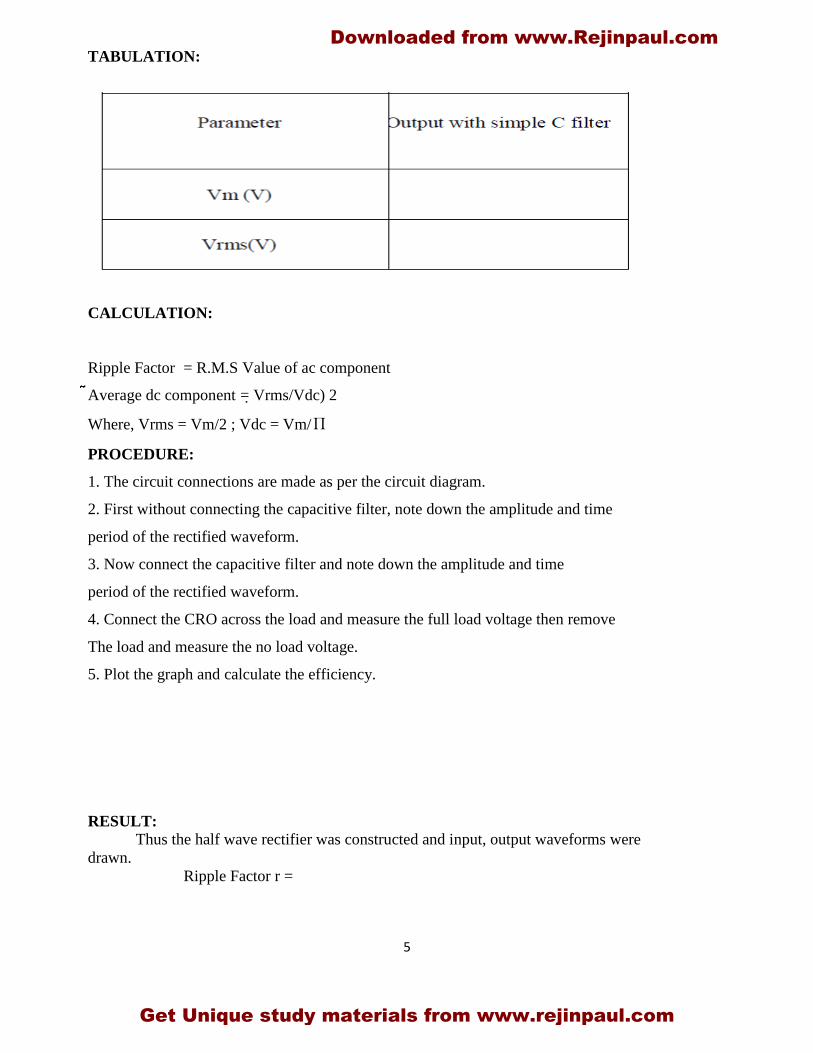
TABULATION:
CALCULATION:
Ripple Factor = R.M.S Value of ac component
Average dc component = Vrms/Vdc) 2
Where, Vrms = Vm/2 ; Vdc = Vm/Π
PROCEDURE:
1. The circuit connections are made as per the circuit diagram.
2. First without connecting the capacitive filter, note down the amplitude and time
period of the rectified waveform.
3. Now connect the capacitive filter and note down the amplitude and time
period of the rectified waveform.
4. Connect the CRO across the load and measure the full load voltage then remove
The load and measure the no load voltage.
5. Plot the graph and calculate the efficiency.
RESULT:
Thus the half wave rectifier was constructed and input, output waveforms were
drawn.
Ripple Factor r =
Downloaded from www.Rejinpaul.com
Get Unique study materials from www.rejinpaul.com

6
FULL WAVE RECTIFIER
AIM:
To construct a full wave rectifier with simple capacitor filter and to measure its ripple
factor from the output waveforms
APPARATUS REQUIRED:
S NO APPARATUS RANGE QUANTITY
1 RESISTOR 1K 2
2 CAPACITOR 100 μf 1
3 DIODE IN4007 2
4 STEP DOWN
TRANSFORMER
1
5 BREAD BOARD 1
6 CONNECTING
WIRES
FEW
7 CRO 1
CIRCUIT DIAGRAM:
Full wave rectifier with filter:
Downloaded from www.Rejinpaul.com
Get Unique study materials from www.rejinpaul.com

7
MODEL GRAPH:
THEORY:
A full wave rectifier is a device which converts ac voltage to pulsating dc voltage using two
PN junction diode.The ac voltage (230 V, 50 HZ) is connected to the primary of the
transformer.The transformer steps down the ac voltage. Thus, with suitable turns ratio we get
desiredac secondary voltage. The rectifier circuit converts this ac voltage in to a pulsating dc
voltage. Full wave rectifier conducts during both positive and negative half cycle of input ac
supply. Because two diodes are used in this cir circuit .It gives output in the form of positive
sinusoidal pulses. Hence the output is called pulsating dc. A pulsating dc voltage containing large
varying component called ripple in it.The capacitor filter is used after rectifier circuit, which
reduces the ripplecontent in the pulsating dc. Thus filter converts pulsating dc in to pure dc.
TABULATION:
Downloaded from www.Rejinpaul.com
Get Unique study materials from www.rejinpaul.com

8
CALCULATION:
Ripple Factor:
The output of the rectifier is of pulsating dc type. The amount of ac content in the
output can be mathematically expressed by a factor called ripple factor.
Ripple Factor = R.M.S Value of ac component
Average dc component = Vrms/Vdc) 2
Where, Vrms = Vm/√2 ; Vdc = 2Vm/Π
PROCEDURE:
1. The circuit connections are made as per the circuit diagram.
2. First without connecting the capacitive filter, note down the amplitude and time
period of the rectified waveform.
3. Now connect the capacitive filter and note down the amplitude and time
period of the rectified waveform.
4. Connect the CRO across the load and measure the full load voltage then remove
theload and measure the no load voltage.
5. Plot the graph and calculate the efficiency.
RESULT:
Thus the full wave rectifier was constructed and input, output waveforms were drawn.
Ripple Factor with filter =
Downloaded from www.Rejinpaul.com
Get Unique study materials from www.rejinpaul.com

9
EXP.NO : 2 DATE:
AIM: To construct a fixed bias amplifier circuit and to plot the frequency response characteristics.
APPARATUS REQUIRED:
S.No. Name Range Quantity 1. Transistor BC107 1 2. Resistor 10 kΩ,100 kΩ,680 Ω 1,1,1 3. Regulated power supply (0-30)V 1 4. Signal Generator (0-3)MHz 1 5. CRO 30 MHz 1
6. Bread Board 1 7. Capacitor 47µ F 2
CIRCUIT DIAGRAM :
FIXED BIAS AMPLIFIER CIRCUIT USING BJT
Downloaded from www.Rejinpaul.com
Get Unique study materials from www.rejinpaul.com

10
MODEL GRAPH :
f 1 f2 f (Hz)
FREQUENCY RESPONSE OF FIXED BIAS AMPLIFIER: Keep the input voltage constant (Vin) =
Frequency (in Hz) Output Voltage (in volts)
Gain = 20 log (Vo / Vin) (in dB)
Downloaded from www.Rejinpaul.com
Get Unique study materials from www.rejinpaul.com

11
FORMULA:
a) R2 / (R1+R2) = voltage at which Class A, Class B or
Class C operation takes place b) hfe = Ic / Ib
THEORY: In order to operate the transistor in the desired region, we have to apply an external dc
voltage of correct polarity and magnitude to the two junctions of the transistor. This is called
biasing of the transistor.
When we bias a transistor, we establish certain current and voltage conditions for the
transistor. These conditions are called operating conditions or dc operating point or quiescent
point. This point must be stable for proper operation of transistor. An important and common
type of biasing is called Fixed Biasing. The circuit is very simple and uses only few components.
But the circuit does not check the collector current which increases with the rise in temperature.
PROCEDURE :
o Connections are made as per the circuit diagram.
o The waveforms at the input and output are observed for Class A, Class B and Class C
operations by varying the input voltages.
o The biasing resistances needed to locate the Q-point are determined.
o Set the input voltage as 1V and by varying the frequency, note the output voltage.
o Calculate gain=20 log (Vo / Vin)
o A graph is plotted between frequency and gain.
CALCULATIONS: a) To determine the value of bias resistace R2 / (R1+ R2)
b) hfe =∆ IC/∆IB RESULT:
Thus, the Fixed bias amplifier was constructed and the frequency response curve is plotted.
ThGain Bandwidth Product is found to be = ______________ .
Downloaded from www.Rejinpaul.com
Get Unique study materials from www.rejinpaul.com

12
EXP.NO : 3 DATE:
AIM:
To constant a voltage divider bias amplifier and measure input resistance and gain and also to plot
the dc collector current as a function of collector resistance.
APPARATUS REQUIRED:
S.No. Name Range Quantity
1. Transistor BC 107 1
2. Resistor 56k ,12k ,2.2k ,470 1,1,1,1
3. Capacitor 0.1µ F, 47µ F 2, 1
4. Function Generator (0-3)MHz 1
5. CRO 30MHz 1
6. Regulated power supply (0-30)V 1
7. Bread Board 1
CIRCUIT DIAGRAM:
BJT AMPLIFIER USING VOLTAGE DIVIDER BIAS
CE-CONFIGURATION
Downloaded from www.Rejinpaul.com
Get Unique study materials from www.rejinpaul.com

13
MODEL GRAPH :
f 1 FIG..2 f2 f (Hz)
Keep the input voltage constant, Vin =
Frequency (in Hz)
Output Voltage (in volts)
Gain= 20 log(Vo/Vin) (in dB)
FORMULA:
Downloaded from www.Rejinpaul.com
Get Unique study materials from www.rejinpaul.com

14
a) Rin = β * Re b) Gain = β * Re/Rin
THEORY:
This type of biasing is otherwise called Emitter Biasing. The necessary biasing is provided using 3
resistors: R1, R2 and Re. The resistors R1 and R2 act as a potential divider and give a fixed voltage to the
base. If the collector current increases due to change in temperature or change in β, the emitter current Ie
also increases and the voltage drop across Re increases, reducing the voltage difference between the base
and the emitter. Due to reduction in Vbe, base current Ib and hence collector current Ic also reduces. This
reduction in Vbe, base current Ib and hence collector current Ic also reduces. This reduction in the collector
current compensates for the original change in Ic.
The stability factor S= (1+β) * ((1/ (1+β)). To have better stability, we must keep Rb/Re as small
as possible. Hence the value of R1 R2 must be small. If the ratio Rb/Re is kept fixed, S increases with β.
PROCEDURE: 1.Connections are given as per the circuit diagram.
2.Measure the input resistance as Rin=Vin/Iin (with output open) and gain by plotting the frequency
response.
3.Compare the theoretical values with the practical values.
4.Plot the dc collector current as a function of the collector resistance (ie) plot of Vcc and Ic for various
values of Re.
RESULT: Thus the voltage divider bias amplifier was constructed and input resistance and gain were determined. The Gain Bandwidth Product is found to be = ____________
Downloaded from www.Rejinpaul.com
Get Unique study materials from www.rejinpaul.com

15
EXP.NO : 4. DATE:
AIM:
To construct a differential amplifier using BJT and to determine the dc collector current of
individual transistors and also to calculate the CMRR.
APPARATUS REQUIRED:
S.No. Name Range Quantity 1. Transistor BC107 2 2. Resistor 4.7kΩ, 10kΩ 2,1 3. Regulated power supply (0-30)V 1 4. Function Generator (0-3) MHz 2 5. CRO 30 MHz 1
6. Bread Board 1 CIRCUIT DIAGRAM:
DIFFERENTIAL AMPLIFIER USING BJT
Downloaded from www.Rejinpaul.com
Get Unique study materials from www.rejinpaul.com

16
OBSERVATION:
VIN =VO =AC = VO / VIN
FORMULA:
Common mode Gain (Ac) = VO / VIN
Differential mode Gain (Ad) = V0 / VIN
Where VIN = V1 – V2
Common Mode Rejection Ratio (CMRR) = Ad/Ac
Where, Ad is the differential mode gain
Ac is the common mode gain.
THEORY:
The differential amplifier is a basic stage of an integrated operational amplifier. It is used to
amplify the difference between 2 signals. It has excellent stability, high versatility and immunity to noise.
In a practical differential amplifier, the output depends not only upon the difference of the 2 signals but
also depends upon the common mode signal.
Transistor Q1 and Q2 have matched characteristics. The values of RC1 and RC2 are equal. Re1 and
Re2 are also equal and this differential amplifier is called emitter coupled differential amplifier. The output
is taken between the two output terminals.
Downloaded from www.Rejinpaul.com
Get Unique study materials from www.rejinpaul.com

17
OBSERVATION:
VIN = V1 – V2
V0 =
Ad = V0/ VIN
For the differential mode operation the input is taken from two different sources and the common
mode operation the applied signals are taken from the same source
Common Mode Rejection Ratio (CMRR) is an important parameter of the differential amplifier.
CMRR is defined as the ratio of the differential mode gain, Ad to the common mode gain, Ac.
CMRR = Ad / Ac In ideal cases, the value of CMRR is very high.
PROCEDURE: 1.Connections are given as per the circuit diagram.
2.To determine the common mode gain, we set input signal with voltage Vin=2V
and determine Vo at the collector terminals. Calculate common mode gain, Ac=Vo/Vin.
3.To determine the differential mode gain, we set input signals with voltages V1 and V2. Compute Vin=V1-
V2 and find Vo at the collector terminals. Calculate differential mode gain, Ad=Vo/Vin.
4.Calculate the CMRR=Ad/Ac.
5.Measure the dc collector current for the individual transistors.
RESULT:
Thus, the Differential amplifier was constructed and dc collector current for the individual
transistors is determined. The CMRR is calculated as _______________
Downloaded from www.Rejinpaul.com
Get Unique study materials from www.rejinpaul.com
18
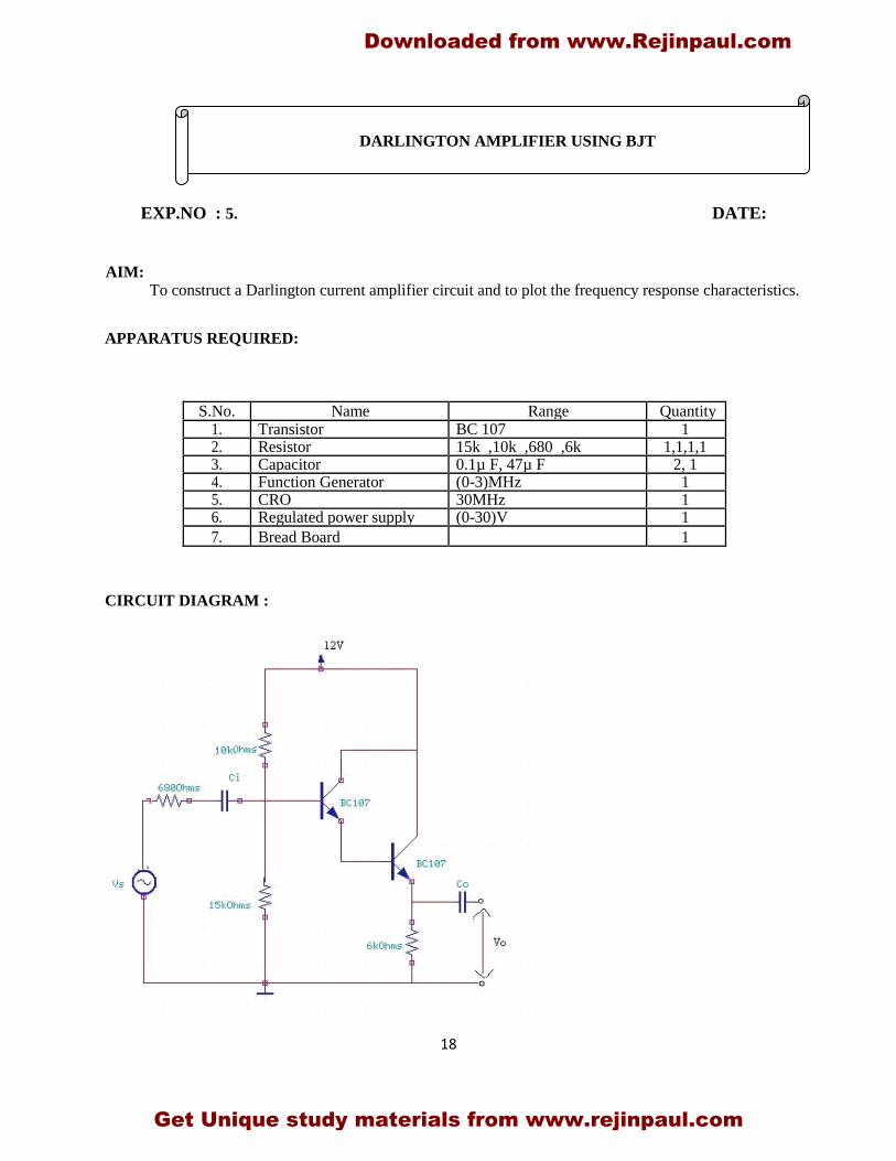
EXP.NO : 5. DATE:
AIM: To construct a Darlington current amplifier circuit and to plot the frequency response characteristics.
APPARATUS REQUIRED:
S.No. Name Range Quantity 1. Transistor BC 107 1 2. Resistor 15k ,10k ,680 ,6k 1,1,1,1 3. Capacitor 0.1µ F, 47µ F 2, 1 4. Function Generator (0-3)MHz 1 5. CRO 30MHz 1 6. Regulated power supply (0-30)V 1
7. Bread Board 1 CIRCUIT DIAGRAM :
DARLINGTON AMPLIFIER USING BJT
Downloaded from www.Rejinpaul.com
Get Unique study materials from www.rejinpaul.com
19
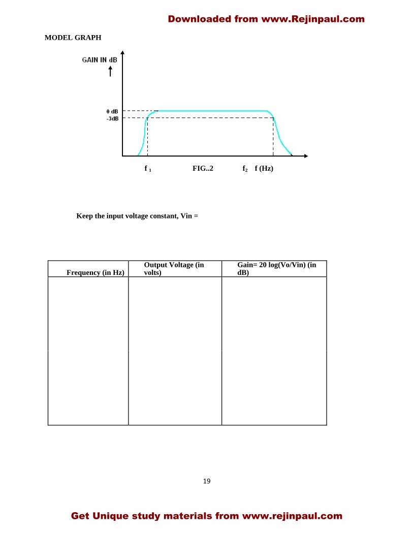
MODEL GRAPH
f 1 FIG..2 f2 f (Hz)
Keep the input voltage constant, Vin =
Frequency (in Hz) Output Voltage (in volts)
Gain= 20 log(Vo/Vin) (in dB)
Downloaded from www.Rejinpaul.com
Get Unique study materials from www.rejinpaul.com

20
THEORY:
In Darlington connection of transistors, emitter of the first transistor is directly connected to the
base of the second transistor .Because of direct coupling dc output current of the first stage is (1+hfe )Ib1.If
Darlington connection for n transitor is considered, then due to direct coupling the dc output current foe
last stage is (1+hfe ) n times Ib1 .Due to very large amplification factor even two stage Darlington
connection has large output current and output stage may have to be a power stage. As the power
amplifiers are not used in the amplifier circuits it is not possible to use more than two transistors in the
Darlington connection.
In Darlington transistor connection, the leakage current of the first transistor is amplified by the
second transistor and overall leakage current may be high, Which is not desired.
PROCEDURE:
1. Connect the circuit as per the circuit diagram.
2. Set Vi =50 mv, using the signal generator.
3. Keeping the input voltage constant, vary the frequency from 0 Hz to 1M Hz in regular steps and note down the corresponding output voltage.
4. Plot the graph; Gain (dB) vs Frequency(Hz).
5. Calculate the bandwidth from the graph.
RESULT:
Thus, the Darlington current amplifier was constructed and the frequency response curve is
plotted. . The Gain Bandwidth Product is found to be = _________________.
Downloaded from www.Rejinpaul.com
Get Unique study materials from www.rejinpaul.com

21
EXP.NO : 6. DATE:
AIM:
To construct a source follower with bootstrapped gate resistance amplifier and plot its frequency response characteristics.
APPARATUS REQUIRED:
S.No. Name Range Quantity
1. Transistor BC107 2
2. Resistor 1kΩ,11 kΩ,1M kΩ 1,1,1
3. Regulated power supply (0-30)V 1
4. Signal Generator (0-3)MHz 1
5. CRO 30 MHz 1
6. Bread Board 1
7. Capacitor 0.01µF 2
SOURCE FOLLOWER WITH BOOTSTRAPPED CIRCUIT
Downloaded from www.Rejinpaul.com
Get Unique study materials from www.rejinpaul.com

22
MODEL GRAPH
f 1 f2 f (Hz)
Keep the input voltage constant (Vin) =
Gain = 20 log (Vo / Vin) (in dB)
frequency (in Hz) Output Voltage (in volts)
Downloaded from www.Rejinpaul.com
Get Unique study materials from www.rejinpaul.com

23
THEORY:
Source follower is similar to the emitter follower( the output source voltage follow the gate input
voltage),the circuit has a voltage gain of less than unity, no phase reversal, high input impedance, low
output impedance. Here the Bootstrapping is used to increase the input resistance by connecting a
resistance in between gate and source terminals. The resister RA is required to develop the necessary bias
for the gate.
PROCEDURE:
1. Connections are made as per the circuit diagram.
2. The waveforms at the input and output are observed for cascode operations by
varying the input frequency.
3. The biasing resistances needed to locate the Q-point are determined.
4. Set the input voltage as 1V and by varying the frequency, note the output voltage.
5. Calculate gain=20 log (Vo / Vin.)
6. A graph is plotted between frequency and gain.
RESULT: Thus, the Source follower with Bootstrapped gate resistance was constructed and the gain was determined.
Downloaded from www.Rejinpaul.com
Get Unique study materials from www.rejinpaul.com

24
EXP NO: 7 DATE :
AIM: To construct a Class A power amplifier and observe the waveform and to compute maximum
output power and efficiency.
APPARATUS REQUIRED:
S.No. Name Range Quantity 1. Transistor CL100, BC558 1,1 2. Resistor 47k ,33 ,220Ω, 2,1 3. Capacitor 47 µ F 2 4. Signal Generator (0-3)MHz 1 5. CRO 30MHz 1 6. Regulated power supply (0-30)V 1
7. Bread Board 1
CIRCUIT DIAGRAM
CLASS - A POWER AMPLIFIER
Downloaded from www.Rejinpaul.com
Get Unique study materials from www.rejinpaul.com

25
TABULATION
Keep the input voltage constant, Vin =
Frequency (in Hz) Output Voltage (in volts) Gain= 20 log(Vo/Vin) (in dB)
FORMULA
Maximum power transfer =Po,max=V
2/R
o L
Effeciency,η = Po,max/Pc
THEORY:
The power amplifier is said to be Class A amplifier if the Q point and the input signal are selected such
that the output signal is obtained for a full input signal cycle.
For all values of input signal, the transistor remains in the active region and never enters into saturation
region. When an a.c signal is applied, the collector voltage varies sinusoidally hence the collector current
also varies sinusoidally.The collector current flows for 3600 (full cycle) of the input signal. i e the angle of
the collector current flow is 3600 .
Downloaded from www.Rejinpaul.com
Get Unique study materials from www.rejinpaul.com

26
PROCEDURE:
1. Connect the circuit as per the circuit diagram.
2. Set Vi =50 mv, using the signal generator.
3. Keeping the input voltage constant, vary the frequency from 10 Hz to 1M Hz in regular steps and note down the corresponding output voltage.
4. Plot the graph; Gain (dB) vs Frequency(Hz).
RESULT:
Thus the Class A power amplifier was constructed. The following parameters were calculated:
a) Maximum output power= ` b) Efficiency=
Downloaded from www.Rejinpaul.com
Get Unique study materials from www.rejinpaul.com
27
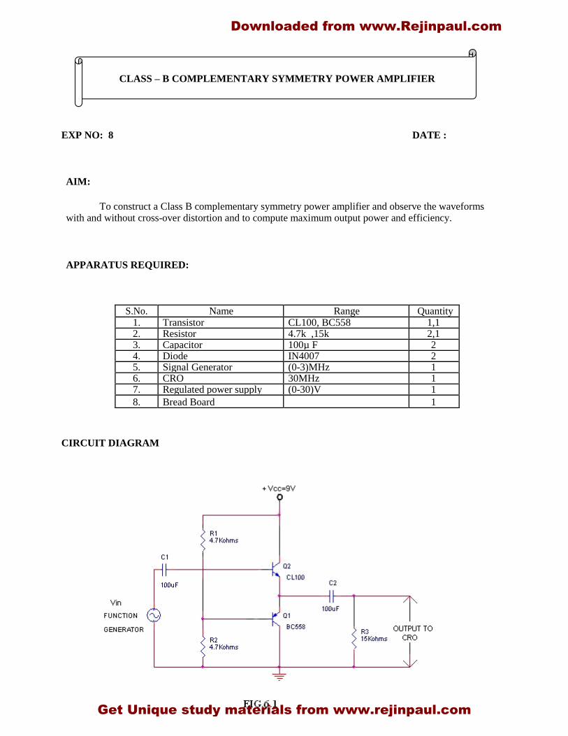
EXP NO: 8 DATE :
AIM:
To construct a Class B complementary symmetry power amplifier and observe the waveforms with and without cross-over distortion and to compute maximum output power and efficiency.
APPARATUS REQUIRED:
S.No. Name Range Quantity 1. Transistor CL100, BC558 1,1 2. Resistor 4.7k ,15k 2,1 3. Capacitor 100µ F 2 4. Diode IN4007 2 5. Signal Generator (0-3)MHz 1 6. CRO 30MHz 1 7. Regulated power supply (0-30)V 1
8. Bread Board 1 CIRCUIT DIAGRAM
CLASS – B COMPLEMENTARY SYMMETRY POWER AMPLIFIER
Downloaded from www.Rejinpaul.com
Get Unique study materials from www.rejinpaul.com

28
FORMULA:
Input power, Pin=2VccIm/П
Output power, Pout=VmIm/2
Power Gain or efficiency, η=л/4(Vm/Vcc) 100 THEORY:
A power amplifier is said to be Class B amplifier if the Q-point and the input signal are selected
such that the output signal is obtained only for one half cycle for a full input cycle. The Q-point is selected
on the X-axis. Hence, the transistor remains in the active region only for the positive half of the input
signal.
There are two types of Class B power amplifiers: Push Pull amplifier and complementary symmetry
amplifier. In the complementary symmetry amplifier, one n-p-n and another p-n-p transistor is used. The
matched pair of transistor are used in the common collector configuration. In the positive half cycle of the
input signal, the n-p-n transistor is driven into active region and starts conducting and in negative half
cycle, the p-n-p transistor is driven into conduction. However there is a period between the crossing of the
half cycles of the input signals, for which none of the transistor is active and output, is zero
CIRCUIT DIAGRAM
FIG.6.2
Downloaded from www.Rejinpaul.com
Get Unique study materials from www.rejinpaul.com

29
OBSERVATION
OUTPUT SIGNAL
AMPLITUDE :
TIME PERIOD :
CALCULATION
POWER, PIN = 2VCC Im/л
OUTPUT POWER,
POUT = VmIm/2
EFFICIENCY, η = ( л/4)( Vm/ VCC) x 100
MODEL GRAPH
Downloaded from www.Rejinpaul.com
Get Unique study materials from www.rejinpaul.com

30
PROCEDURE: 1. Connections are given as per the circuit diagram without diodes.
2. Observe the waveforms and note the amplitude and time period of the input signal and distorted waveforms.
3. Connections are made with diodes. 4. Observe the waveforms and note the amplitude and time period of the input signal and output
signal. 5. Draw the waveforms for the readings.
6. Calculate the maximum output power and efficiency. Hence the nature of the output signal gets distorted and no longer remains the same as the input.
This distortion is called cross-over distortion. Due to this distortion, each transistor conducts for less than
half cycle rather than the complete half cycle. To overcome this distortion, we add 2 diodes to provide a
fixed bias and eliminate cross-over distortion.
RESULT:
Thus the Class B complementary symmetry power amplifier was constructed to observe cross-
over distortion and the circuit was modified to avoid the distortion. The following parameters were
calculated:
a)Maximum output power= b)Efficiency=
Downloaded from www.Rejinpaul.com
Get Unique study materials from www.rejinpaul.com

31
Downloaded from www.Rejinpaul.com
Get Unique study materials from www.rejinpaul.com
32
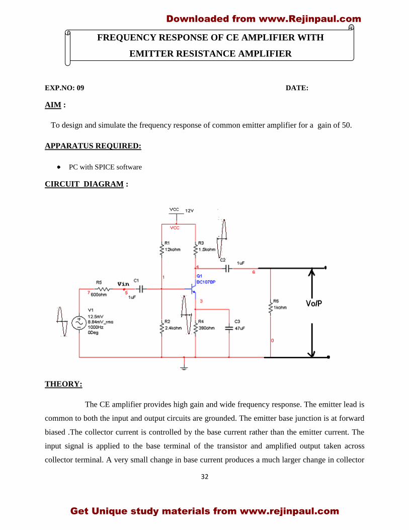
EXP.NO: 09 DATE:
AIM :
To design and simulate the frequency response of common emitter amplifier for a gain of 50.
APPARATUS REQUIRED:
PC with SPICE software
CIRCUIT DIAGRAM :
THEORY:
The CE amplifier provides high gain and wide frequency response. The emitter lead is
common to both the input and output circuits are grounded. The emitter base junction is at forward
biased .The collector current is controlled by the base current rather than the emitter current. The
input signal is applied to the base terminal of the transistor and amplified output taken across
collector terminal. A very small change in base current produces a much larger change in collector
FREQUENCY RESPONSE OF CE AMPLIFIER WITH
EMITTER RESISTANCE AMPLIFIER
Downloaded from www.Rejinpaul.com
Get Unique study materials from www.rejinpaul.com

33
current. When the positive is fed to input circuit it opposes forward bias of the circuit which cause
the collector current to decrease, it decreases the more negative. Thus when input cycle varies
through a negative half cycle, increases the forward bias of the circuit, which causes the collector
current increases .Thus the output signal in CE is out of phase with the input signal.
PROCEDURE
1. Select different components and place them in the grid.
2. For calculating the voltage gain the input voltage of 25mv (p-p) amplitude and 1KHz
frequency is applied, then the circuit is simulated and output voltage is noted.
3. The voltage gain is calculated by using the expression
Av = Vo/Vi
4. For plotting frequency response, the input voltage is kept constant at 25mv(p-p) and
frequency is varied.
5. Note down the output voltage for each frequency.
6. All readings are tabulated and Av in db is calculated using the formula
20 Log Vo/Vi.
7. A graph is drawn by taking frequency on X-axis and gain in dB on Y-axis on a Semi log
graph sheet.
SPICE FILE :
VIN 1 4 SIN(0 1.5V 2KHZ)
VB 4 0 2.3V
RL 3 0 15K
V1 2 0 15V
Q1 2 1 3 MOD1
.MODEL MOD1 NPN
.TRAN 0.02MS 0.78MS
.PROBE
.END
Downloaded from www.Rejinpaul.com
Get Unique study materials from www.rejinpaul.com

34
THEORITICAL CALCULATIONS :
To calculate Av, Zin(base) and Z in :
Downloaded from www.Rejinpaul.com
Get Unique study materials from www.rejinpaul.com

35
PRACTICAL CALCULATIONS :
INPUT WAVE FORM :
OUT PUT WAVE FORM :
RESULT:
Thus the simulation of class-B amplifier using PSPICE was simulated
successfully.
Downloaded from www.Rejinpaul.com
Get Unique study materials from www.rejinpaul.com

36
EXP.NO: 10 DATE:
AIM:
To find the DC response of CS amplifier.
APPARATUS REQUIRED:
PC with SPICE software
CIRCUIT DIAGRAM:
THEORY:
In electronics, a common-source amplifier is one of three basic single-stage field-effect transistor
(FET) amplifier topologies, typically used as a voltage or transconductance amplifier. The easiest
way to tell if a FET is common source, common drain, or common gate is to examine where the
signal enters and leaves. The remaining terminal is what is known as "common". In this example,
the signal enters the gate, and exits the drain. The only terminal remaining is the source. This is a
common-source FET circuit. The analogous bipolar junction transistor circuit is the common-
emitter amplifier.
The common-source (CS) amplifier may be viewed as a transconductance amplifier or as a voltage
amplifier. (See classification of amplifiers). As a transconductance amplifier, the input voltage is
seen as modulating the current going to the load. As a voltage amplifier, input voltage modulates
the amount of current flowing through the FET, changing the voltage across the output resistance
DC RESPONSE OF CS AMPLIFIER
Downloaded from www.Rejinpaul.com
Get Unique study materials from www.rejinpaul.com

37
according to Ohm's law. However, the FET device's output resistance typically is not high enough
for a reasonable transconductance amplifier (ideally infinite), nor low enough for a decent voltage
amplifier (ideally zero). Another major drawback is the amplifier's limited high-frequency
response. Therefore, in practice the output often is routed through either a voltage follower
(common-drain or CD stage), or a current follower (common-gate or CG stage), to obtain more
favorable output and frequency characteristics. The CS–CG combination is called a cascode
amplifier.
PROCEDURE:
1.Measure the DC operating point of each transistor and compare your results with the calculated
values.
2.At a frequency of 5 KHz, measure the voltage gain, the input and the output resistance and
compare your results withthe theoretical values. Calculate the power gain from both experimental
and theoretical values.
3.Find the maximum peak-to-peak output voltage swing (i.e. the maximum swing without
distortion).
4.Measure the frequency response of the circuit and comment on the change observed in
comparison with a single stage common-emitter amplifier.
5.Simulate the circuit using Pspice. Compare the Pspice results with those obtained in the previous
parts.
OUTPUT WAVEFORM:
RESULT:
Thus the simulation of DC response of CS amplifier was simulatdd successfully.
Downloaded from www.Rejinpaul.com
Get Unique study materials from www.rejinpaul.com

38
EXP.NO: 11 DATE:
AIM:
To determine the frequency response of Cascode Amplifier.
APPARATUS REQUIRED:
PC with SPICE software
CIRCUIT DIAGRAM:
THEORY:
Cascode amplifier is a two stage circuit consisting of a transconductance amplifier followed by a
buffer amplifier. The word “cascode” was originated from the phrase “cascade to cathode”. This
circuit have a lot of advantages over the single stage amplifier like, better input output isolation,
better gain, improved bandwidth, higher input impedance, higher output impedance, better
stability, higher slew rate etc. The reason behind the increase in bandwidth is the reduction of
FREQUENCY RESPONSE OF CASCODE AMPLIFIER
Downloaded from www.Rejinpaul.com
Get Unique study materials from www.rejinpaul.com

39
Miller effect. Cascode amplifier is generally constructed using FET ( field effect transistor) or BJT
( bipolar junction transistor). One stage will be usually wired in common source/common emitter
mode and the other stage will be wired in common base/ common emitter mode.
Miller effect.
Miller effect is actually the multiplication of the drain to source stray capacitance by the voltage
gain. The drain to source stray capacitance always reduces the bandwidth and when it gets
multiplied by the voltage gain the situation is made further worse. Mulitiplication of stray
capacitance increases the effective input capacitance and as we know, for an amplifier, the increase
in input capacitance increases the lower cut of frequency and that means reduced bandwidth.
Miller effect can be reduced by adding a current buffer stage at the output of the amplifier or by
adding a voltage buffer stage before the input.
PROCEDURE:
1.Measure the DC operating point of each transistor and compare your results with the calculated
values.
2.At a frequency of 5 KHz, measure the voltage gain, the input and the output resistance and
compare your results withthe theoretical values. Calculate the power gain from both experimental
and theoretical values.
3.Find the maximum peak-to-peak output voltage swing (i.e. the maximum swing without
distortion).
4.Measure the frequency response of the circuit and comment on the change observed in
comparison with a single stage common-emitter amplifier.
5.Simulate the circuit using Pspice. Compare the Pspice results with those obtained in the previous
parts.
MODEL GRAPH
RESULT:
Thus she simulation of frequency response of Cascode Amplifier was simulated.
Downloaded from www.Rejinpaul.com
Get Unique study materials from www.rejinpaul.com

40
EXP.NO: 12 DATE:
AIM:
To simulate the Class-B amplifier by using PSICE.
APPARATUS REQUIRED:
PC with SPICE software
CIRCUIT DIAGRAM:
Class B Amplifier
THEORY:
Class-B amplifiers improve the efficiency of the output stage by eliminating quiescent
power dissipation by operating at zero quiescent current. This is implemented in Figure 2. As the
input voltage V swings positive, M1 turns on when V exceeds the threshold voltage , and the
output voltage follows the input on the positive swing. When the input voltage swings negative,
M2 turns on when is less than threshold voltage , and the output voltage follows the input on the
negative swing. There is a “dead zone” in the class-B voltage transfer characteristic, where both
transistors are not conducting.
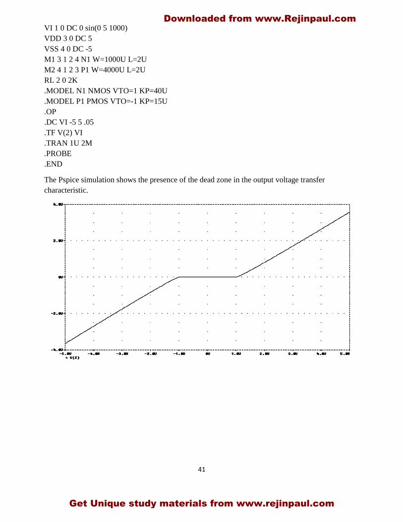
The class-B amplifier is simulated the netlist is shown below:
* Class B Amplifier
*Filename=”classb.cir”
TRANSFER CHARACTERISTICS OF CLASS-B POWER AMPLIFIER
Downloaded from www.Rejinpaul.com
Get Unique study materials from www.rejinpaul.com
41
VI 1 0 DC 0 sin(0 5 1000)
VDD 3 0 DC 5
VSS 4 0 DC -5
M1 3 1 2 4 N1 W=1000U L=2U
M2 4 1 2 3 P1 W=4000U L=2U
RL 2 0 2K
.MODEL N1 NMOS VTO=1 KP=40U
.MODEL P1 PMOS VTO=-1 KP=15U
.OP
.DC VI -5 5 .05
.TF V(2) VI
.TRAN 1U 2M
.PROBE
.END
The Pspice simulation shows the presence of the dead zone in the output voltage transfer
characteristic.
Downloaded from www.Rejinpaul.com
Get Unique study materials from www.rejinpaul.com

42
The current in each transistor conducts for less than half cycle. M1 conducts in the positive
half cycle and M2 in the negative half cycle.
The transient analysis shows that the dead zone causes a distortion in the output waveform.
RESULT:
Thus the simulation of class-B amplifier using PSPICE was simulated successfully.
Downloaded from www.Rejinpaul.com
Get Unique study materials from www.rejinpaul.com

43
EXP.NO: 13 DATE:
AIM:
To simulate the design of DC power supply using by using PSICE.
APPARATUS REQUIRED:
PC with SPICE software
CIRCUIT DIAGRAM:
HALF WAVE RECTIFIER:
THEORY:
In half wave rectification, either the positive or negative half of the AC wave is passed,
while the other half is blocked. Because only one half of the input waveform reaches the output, it
is very inefficient if used for power transfer. Half-wave rectification can be achieved with a single
diode in a one-phase supply, or with three diodes in a three-phase supply. Half wave rectifiers yield
a unidirectional but pulsating direct current.
SPICE FILE :
V1 1 0 SIN(0 10V 100HZ)
R 1 2 1K
DA 0 2 D1
.MODEL D1 D
.TRAN 0.01MS 20MS
.PROBE
.END
DESIGN OF A DC POWER SUPPLY USING RECTIFIER
Downloaded from www.Rejinpaul.com
Get Unique study materials from www.rejinpaul.com
44
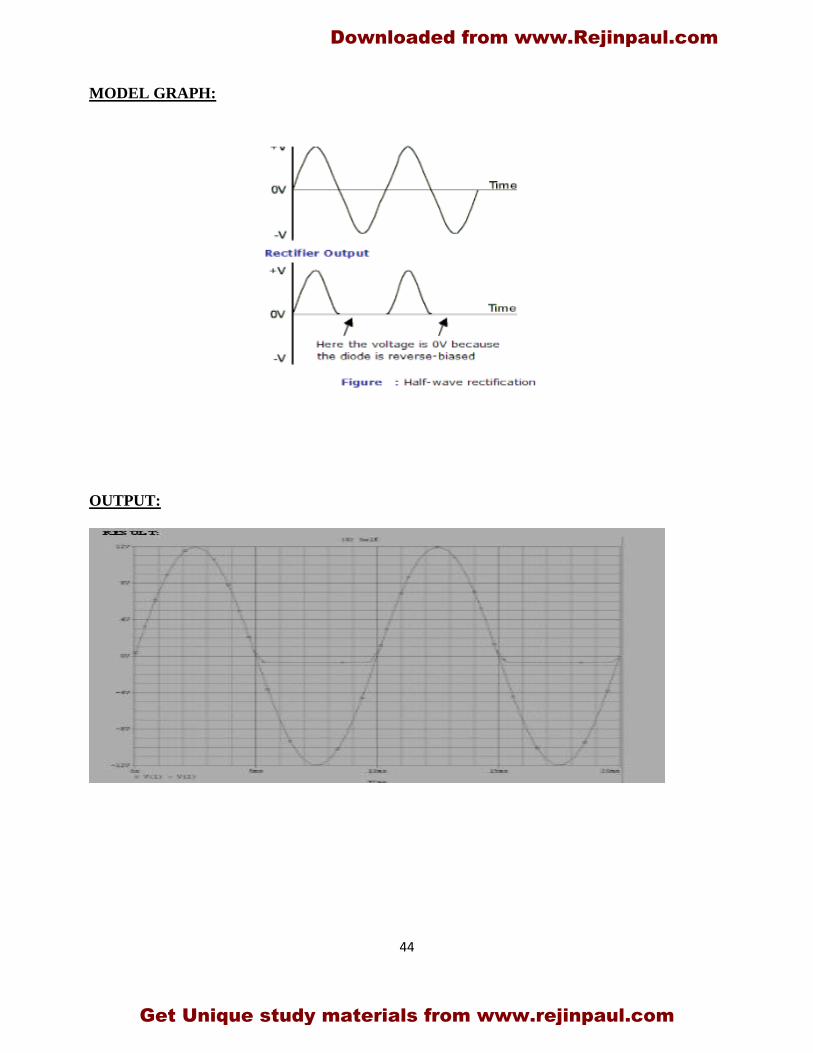
MODEL GRAPH:
OUTPUT:
Downloaded from www.Rejinpaul.com
Get Unique study materials from www.rejinpaul.com

45
FULLWAVE RECTIFIER:
CIRCUIT DIAGRAM:
THEORY:
A full-wave rectifier converts the whole of the input waveform to one of constant polarity
(positive or negative) at its output. Full-wave rectification converts both polarities of the input
waveform to DC (direct current), and is more efficient.
SPICE FILE :
V1 1 0 SIN(0 10V 100HZ)
R 2 3 1K
C 2 3 1N
D1 1 2 MOD1
D2 0 2 MOD1
.MODEL MOD1 D
.TRAN 0.01MS 20MS
PROBE
.END
Downloaded from www.Rejinpaul.com
Get Unique study materials from www.rejinpaul.com

46
GRAPH:
OUTPUT:
RESULT:
Thus the simulation of design of a DC power supply using Rectifier was simulated.
Downloaded from www.Rejinpaul.com
Get Unique study materials from www.rejinpaul.com