LAB EXERCISE 7.1 UP/DOWN Counters Objectives Materials ...
13
18. What is a universal shift register? In this lab exercise we will study ripple counters. We implement up and down counters using discrete flip-flop ICs. will LAB EXERCISE 7.1 UP/DOWN Counters Objectives LD-2 Logic Designer Materials 74LS76 Dual J-K Flip-flops with Preset and Clear Jumper Wires TIL Da ta Book 1. In this portion of the laboratory, we will construct an up- counter using J-K flip-flops. Procedure 2. Wire the circuit shown in Figure 7-16. Use extra caution wiring the power and ground connections. Vee L1 L2 FIGURE 7-'6 . Up Counter. 7 s 4 Qt--OolII:......... 9 - PB2 .s-L 2I274LS76 143
Transcript of LAB EXERCISE 7.1 UP/DOWN Counters Objectives Materials ...

18. What is a universal shift register?
In this lab exercise we will study ripple counters. We implement up and down counters using discrete flip-flop ICs.
will LAB EXERCISE 7.1 UP/DOWN Counters Objectives
LD-2 Logic Designer Materials
74LS76 Dual J-K Flip-flops with Preset and Clear
Jumper Wires
TIL Da ta Book
1. In this portion of the laboratory, we will construct an upcounter using J-K flip-flops.
Procedure
2. Wire the circuit shown in Figure 7-16. Use extra caution wiring the power and ground connections.
Vee L1 L2 FIGURE 7-'6. Up Counter.
7 s
4 Qt--OolII:......... 9
- PB2 .s-L ----4-~C ~-+-~C
PB'lJ'--------~~----------~ 2I274LS76
143

3. Tum-on power to the LD-2. Push PBI. All lights except for 01 should be off.
4. Use PB2 as the clock input, Ll and L2 as the 1 and 2 outputs. Record your observations of the circuit operation.
'.' " " . : ~:. ' " ,, :,' '~ · '; f it ~ :"!,, "!' . ~~ .. .. ... . .... :.' .... . . . , .. . .. ,.. .• · :." '. 5. UsePB2t6 placea ·;courtt ,of two on Ll andt.2~ Press PBI .
;~. and record your observation.
6. Tum off power to the LO-2. Remove the wires from pin 15 of the 74LS76 and place them on pm 14.
7. Remove the wire from pin 11 of the 74L576 and place it on pin 10.
8. Tum-on power to the circuit. Push PBI. Ll, L2 and 01 should light.
9. Use PB2 as the clock input and Ll and L2 as the 1 and 2 . outputs. Notice that the Ll and L20utputs will now be LO true so that the count when both lights are ON is zero. Record your observations of the circuit operation.
Questions 1. What is .the modulus of each of . the counters in this laboratory ?

2. How can the down counter be converted to display a HI true output?
In this lab exercise we will study synchronous counters. We will implement simple synchronous counters using flip-flop ICs. We will study both up and down counters.
LD-2 Logic Designer
74LS76 Dual J-K Flip-flops with Preset and Clear
Jumper Wires
TIL Data Book
Procedure
1. Place a 74LS76 on the LD-2 breadboard and wire the circuit shown in Figure 7-17.
L1 L2
Vee
~..,i
1
J..§..
12 S
J a 15
C -
K a ~ R .... 3
17 S
9 J a
6 ~C
Jl. K a RTs
t-1l.
~
F~' 1.S PB2 JL
LAB EXERCISE 7.2 Synchronous Counters
Objectives
Materials
Procedure
FIGURE 7-17. Synchronous Up Counter.
145

2. Tum · on power to the LD-2 and push PBl. Only D1 should be lit.
3. Use PB2 as the count input and L1 and L2 as the count outputs. Record your observations of the operation of this circui t.
4. Remove power from the LD-2. Remove the wires from pin 15 of the 74LS76 and wire them to pin 14.
5. Remove the wire from pin 11 of the 74LS76 and place the wire to pin 10.
6. Tum on power to the LD-2. Push PB1. Ll, L2 and Dl should light.
7. Use PB2 as (he count input and record your observations of the circuit operation. Again, notice that the Ll and L2 outputs are LO true.
Questions 1. Fully describe both counter circuits in this laboratory.
LAB EXERCISE 7.3 IC Counters In this lab exercise we will study !C_ counters. The two types of
counters studied will be the 74l59O decade counter and the 74193 Objectives synchronous 4-bit binary up/down counter.
Materials LD-2 Logic Designer
74LS90 Decade Counter 146

74114j3 -4-lJIT Binary twlDOWN COlll'De£
jwm:,1f!' Wires .
TTl. Data Book
1. The irst counter IC wWed will be the 74LS90. This ciirc:Jit contains sepwmadelfivide by two and divide by five sedlimts. To fomI ~ decade CQWltel we will intemnnect the; ~ tt the divide by two section to the mput of the cfivnd'e !Joy five section. This choice is acl!Jttrary and the aIll!emative method will also form a decade counter.
2. Wmre the circuit silown in Egure 7-18. Notice t.IJ:JOltlventional arr.il!ng£ililll!!lt of the power pins. Wft 052 DE to +5 VDC.
T.490
Vee ...-_ P81.Il...
D S
P82Il...2 A
3. Tum on power to the iD-2. Push PB1. Dl should light
and 052 should display il zero.
4. Use PB2 as the colImt mput and 052 as the output. Rerotd your obse~ of the operation of this counter circuit.
the Also,
Procedure
FIGURE 7·18. Decade Counter.
147

5. Set the counter to some non-zero count and press PSI. '--
Record your observations.
6. Remove power from the LD-2 apd re~ove the 74LS90 and it's circuitry.
7.Wir~the circuit shown ip Figure 7-19 usmg the 74193 Ie counter.
PBilSFIGURE 7·19. 4·Bit Binary
. :1 . PB2 Up/Down Counter.
--
8. Set 55' to La and 54 to HI. These are the CLEAR and LOAD inputs . res~vely. Tum on ' power to the LD-2. Place 55 from LO ..to,tilthenback toLD. Only 01 should be lit.
9. This circuit reqUireS'some,explariatiC:)ll. so-S4 are data inputs which are loaded as presets to the counter under command of theLOADcontrollme(54). UsePB1 &PS2 to count up or down respectively. Another way to observe the operation of this counter is by changing SO-SS from HI to La. Record the difference ofthe twooperations..
74193
148

10. Remove power from the LD-2 and answer the questions below.
1. Will the counter count with,Ute load input active? Questions
2. Can the counter be loaded with the dear input active?
3. What is the modulus of this counter?
4. How could you make a counter of modulus 7 using the 74193 ?
In this lab exercise you will study two types of shift registers. You will use the 74174 IC to construct both parallel-in/parallelout and serial-in/ serial-out shift registers.
LD-2 Logic Designer
74174 Hex D Flip-flops with Clear IC
74LS08 Quadruple 2 Input Positive AND Gate
74LS32 Quadruple 2 Input Positive OR Gate
Jumper Wires
TIL Data Book
LAB EXERCISE 7.4 Shift Registers
Objectives
Materials
1.
2.
You will study the SISQ configuration of the 74174 first. Wire the circuit shown in Figure 7-20. Tum on power and push PBl. D1 should light.
Procedure
149

--
(3)
FIGURE 7·20. SISO Shift Register.
60
0 a .1- to.. CK
I""
Clear
(2)10 0 Q f--4~ 10
S1 .... CK... I""
Clear
V (4) (5)
20 1 0 0 -4~20
--~CK Clear y
3D (6) 1 (7)
Q0 -30L3-.... ~CK
Clear y
(11 ) (10) 4D ~40
y
(13) 0 Q
~CK
Clear
(12) -5050
~
14) (15)( 0 0
"~CK (9)
Clear
sa
Gates 4,5,6 Not Used
Clock PB2J1.
(1 ) _IClear PB1U
~

3. Use Sl as the input bit, PB2 as the clock pulse and L3 as the output. Record your observation of the operation of this circuit.
4. Press PB1. Place Sl to HI and press PB2 until L3 lights. Now press PB1. Record your observations.
5. Some additional circuitry will be required to allow us to use the 74174 as a parallel loading shift register. Wire the circuit shown in Figure 7-21.
----"""'"'l.._...1
74LS32
6 0
FIGURE 7-21. 74174 PIPO S, ______~
t-"3~_ ___'3""1D 0.,:2.....__ L1 Shift Register. PB1Jl----------~2~
CK 74LS08112
1/4 CLR
PB2U_______"'"4
3 4 0 0~5""__L2 PBdL____"'"'1
S2---~'_I
PB2 U
PB1 fl-----:.Kot 0 r:-7----L3 53 ---.:..::~
2/4 CK
PB2 n---.::9-4 CLR
S4-.....:....t
74LS08111 74174 414 316

6. Place all 51-54 to off. Turn on power. D1 should light.
7. Use 51-53 as the parallel inputs, 54 as the clear input, PB1 . as the load enable input, PB2 as the clock input and L1'-L3 as the parallel outputs. Observe the operation of this circuit and record your observations. Notice that to load the parallel data you must hold the enable pushbutton down.
Questions 1. Explain the operation of the gating between flip-flops in Figure 7-21.
circuits appearing
2. Do you have to reset the 74174 in step seven to load '--parallel data ?
3. Could you make a PIPO shift register using only the 74174 and the two OR gates? What would be the operational restrictions on such a circuit?
LAB EXERCISE 7.5 The 74165 In this lab exercise you will study the 74165 Ie. You will
implement a PISO shift register using the 74165 and observe it's Objectives use as a 5150.
Materials LD-2 Logic Designer
74165 Parallel Load Eight-bit 5hift Register
152

-- -
Jumper Wires
TTL Data Book
1. Install a 74165 Ie on the LD-2 breadboard and wire the Procedure circuit shown in Figure 7-22.
r---PB2Jl
GND OH H G
FIGURE 7·22. 74165 PISO Shift Register.
-
2. Place all logic switches to off. Turn on power. D1 should light.
3. Use PBl as the load input, PB2 as the clock input, SO-57 as the data input and LO as the output. Record your
observations about the operation of this circuit.
4. Tum off power and remove th", wire connecting pin 10 to ground. Place all logic switches to off. Again observe the circuit operation and record your observations.
153
Questions 1. How does the 74165 determine which input tQ receive it's data from. Describe how each data input is activated .
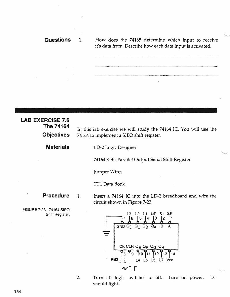
LAB EXERCISE 7.6 The 74164
Objectives
Materials
Procedure
FIGURE 7·23. 74164 SIPO Shift Register.
In this lab exercise we will study the 74164 IC You will use the 74164 to implement a SIEO shift register.
LD-2 Logic Designer
74164 8-Bit Parallel Output Serial Shift Register
Jumper Wires
TIL Data Book
1. Insert a 74164 Ie into the LD-2 breadboard and wire the circuit shown in Figure 7-23.
14
L4 L5 L6 L7 Vee
PS1U
2. Turn all logic switches to off. Turn on power. D1 should light.
154
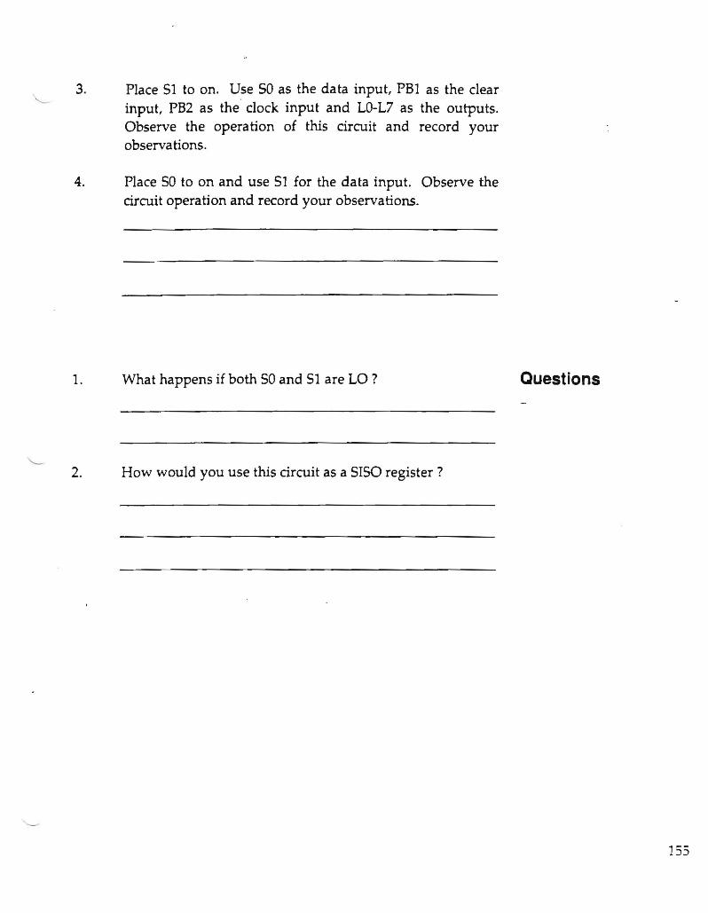
3. Place 51 to on. Use SO as the data input, PBl as the clear input, PB2 as the clock input and LO-L7 as the outputs. Observe the operation of this circuit and record your observa tions.
4. Place 50 to on and use 51 for the data input. Observe the circuit operation and record your observations.
1. What happens if both 50 and 51 are LO? Questions
2. How would you use this circuit as a 5ISO register?
153