Lab 10. Speed Control of a D.C. motor
32
Lab 10. Speed Control of a D.C. motor Speed Measurement: Tach Amplitude Method References: STM32L100 Data Sheet (pin definitions) STM32L100 Ref. Manual (ADC, GPIO, Clocks)
Transcript of Lab 10. Speed Control of a D.C. motor

Lab 10. Speed Control of a D.C. motor
Speed Measurement:Tach Amplitude MethodReferences: STM32L100 Data Sheet (pin definitions)
STM32L100 Ref. Manual (ADC, GPIO, Clocks)

Motor Speed Control Project1. Generate PWM waveform2. Amplify the waveform to drive the motor3. Measure motor speed4. Measure motor parameters5. Control speed with a PID controller
ComputerSystem
12v dcMotor Tachometer
Frequency toVoltage
Analog toDigital
Amplifier9 v
PowerSupply
ac-to-dc
Lab 10

Typical analog input subsystem
inputtransducer
signalconditioning
sample& hold
Analog todigital conv.
Property1
Digital value
mux
inputtransducer
signalconditioning
Property2
inputtransducer
signalconditioning
PropertyN
select channel
…
STM32L1xx---------------16 channels,12-bit ADC
convert “property” to electrical voltage/current
produce convenient voltage/current levels over range of interest
hold value during conversion
convert analog value to digital #

Signal conditioning
Produce noise-free signal over A/D converter input range Convert AC signal to DC form
Needed in this lab to measure tachometer signal amplitude
Amplify/attenuate voltage/current levels Tachometer voltage might be > max ADC input range
Bias (shift levels to desired range) Filter to remove noise Common mode rejection for differential signals Isolation/protection (optical/transformer)
STM32L100-Discovery : [0v to 3v]
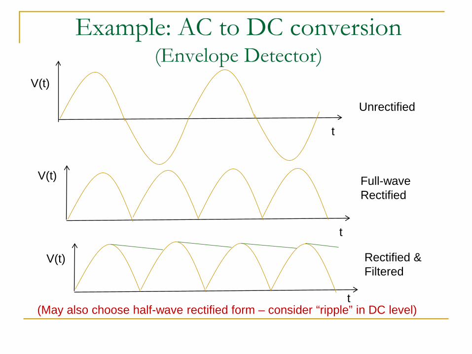
Example: AC to DC conversion(Envelope Detector)
V(t)
t
V(t)
t
V(t)
t
Unrectified
Full-waveRectified
Rectified &Filtered
(May also choose half-wave rectified form – consider “ripple” in DC level)

V(t)
t
V(t)
t
V(t)
t
Unrectified
Half-waveRectified
Rectified &Filtered
larger RC
smaller RC
Example: AC to DC conversion(Envelope Detector)

Tach signal
RectifiedRectified signal:Is output “ripple” acceptable?
Is the DC level acceptable?
Rectifier FilterTachsignal
Signal conditioningto measure tach signal amplitude
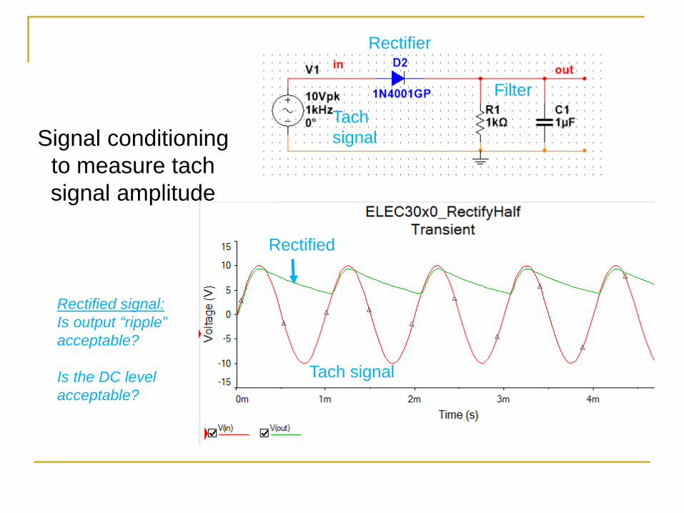
Tach signal
Rectified
Rectified signal:Is output “ripple” acceptable?
Is the DC level acceptable?
Rectifier
FilterTachsignalSignal conditioning
to measure tachsignal amplitude

Analog to digital conversion
Given: continuous-time electrical signal v(t), t >=0
Desired: sequence of discrete numeric values that represent the signal at selected sampling times :
v(0), v(T), v(2T),…v(nT) v(nT) = v(t) value measured at the nth sample time
Quantized to one of 2k discrete levels Produces a k-bit number
T = “sampling time” v(t) is “sampled” every T seconds Sampling frequency Fsample = 1/T

A/D conversion processv(t)
t
T 2T 3T 4T 5T 6T 7T 1 2 3 4 5 6 7
v(t*)
t* n
v(nT)
Input signal
Sampled signal(3/4)Vref
Sampled & Quantized
Sampled data sequence:n= 1 2 3 4 5 6 7d=10, 10, 10, 10, 11, 11, 11
binary datav(nT) = (d/4)Vref
(2/4)Vref
(1/4)Vref
(0/4)Vref
1
2
3
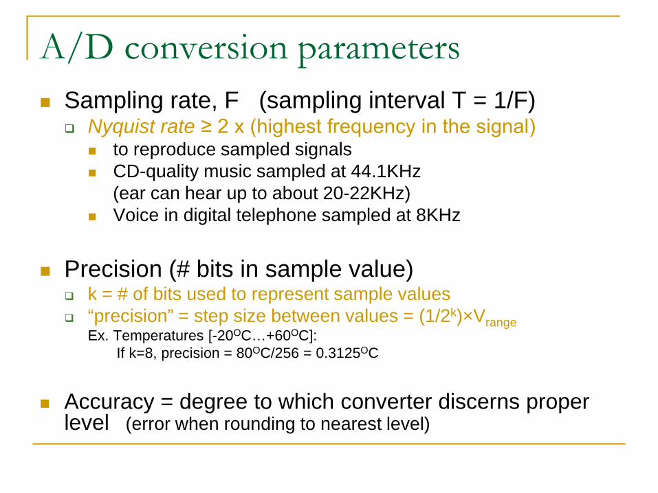
A/D conversion parameters Sampling rate, F (sampling interval T = 1/F)
Nyquist rate ≥ 2 x (highest frequency in the signal) to reproduce sampled signals CD-quality music sampled at 44.1KHz
(ear can hear up to about 20-22KHz) Voice in digital telephone sampled at 8KHz
Precision (# bits in sample value) k = # of bits used to represent sample values “precision” = step size between values = (1/2k)×Vrange
Ex. Temperatures [-20OC…+60OC]: If k=8, precision = 80OC/256 = 0.3125OC
Accuracy = degree to which converter discerns proper level (error when rounding to nearest level)
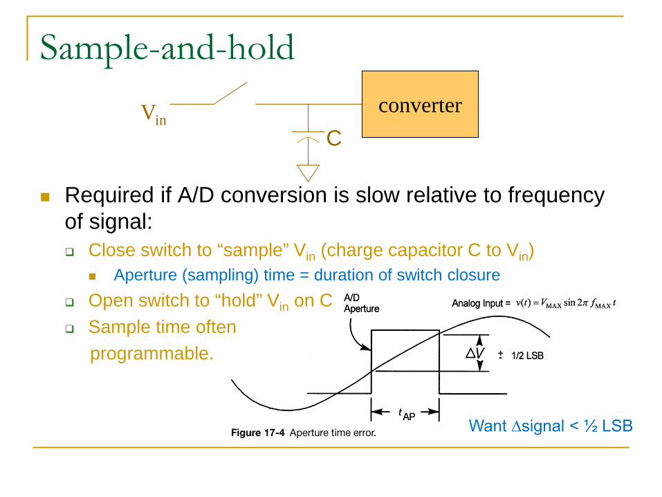
Sample-and-hold
Required if A/D conversion is slow relative to frequency of signal: Close switch to “sample” Vin (charge capacitor C to Vin)
Aperture (sampling) time = duration of switch closure Open switch to “hold” Vin on C Sample time often
programmable.
converterVinC
Want ∆signal < ½ LSB
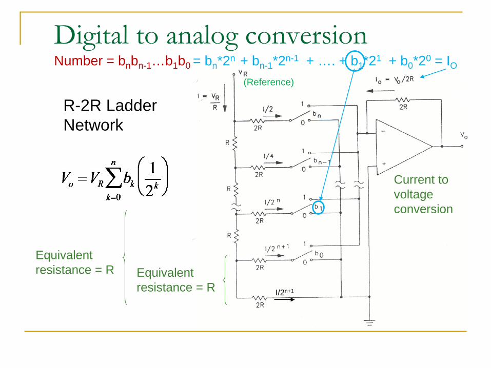
Digital to analog conversion
R-2R Ladder Network
(Reference)
Equivalent resistance = R I/2n+1
Equivalent resistance = R
Current tovoltageconversion
Number = bnbn-1…b1b0 = bn*2n + bn-1*2n-1 + …. + b1*21 + b0*20 = IO

Successive approximation analog to digital converter (ADC)
1. Successive Approximation Register (SAR) sets DN-1 = 1
2. SAR outputs DN-1 … D0, convertedby DAC to analog VDAC
3. VDAC is compared to VIN4. Comparator output resets DN-1 to 0
in SAR if VDAC < VIN5. Repeat 1-4 for DN-2 … D0
(one clock period per bit)
• Final SAR value DN-1 … D0 is digital representation of VIN
End of conversion
VIN captured in S/H
VDAC
• Determine one bit at a time, from MSB to LSBUsed in most microcontrollers (low cost)
VIN
Output

STM32L100RC Analog to Digital Converter Successive approximation ADC Input range: VREF- ≤ VIN ≤ VREF+ (3.6 v max)
Discovery Board: VREF+ = VDDA pin, hard-wired to VDD (+3v)VREF- = VSSA pin, hard-wired to GND ( 0v)
Selectable resolution: 12, 10, 8, or 6 bits (default=12) TCONVERT = 12, 11, 9, 7 clock cycles, respectively
Programmable sampling time TSAMPLE = 4 to 384 clock cycles Minimum conversion time 1µs (TSAMPLE + TCONVERT ) 22 input channels
GPIO pins: ADC_IN[0:15], ADC_IN[18:21] - on designated GPIO pins Temperature sensor & voltage reference: ADC_IN[16:17]
Single or continuous conversions Scan mode for conversion of multiple channels Interrupt at end of conversion or end of sequence Trigger conversions with software or hardware (timers/EXTI)

ADC System Components
Analoginputs
ADC
Clock
Data register
Referencevoltage
Channelselection Trigger
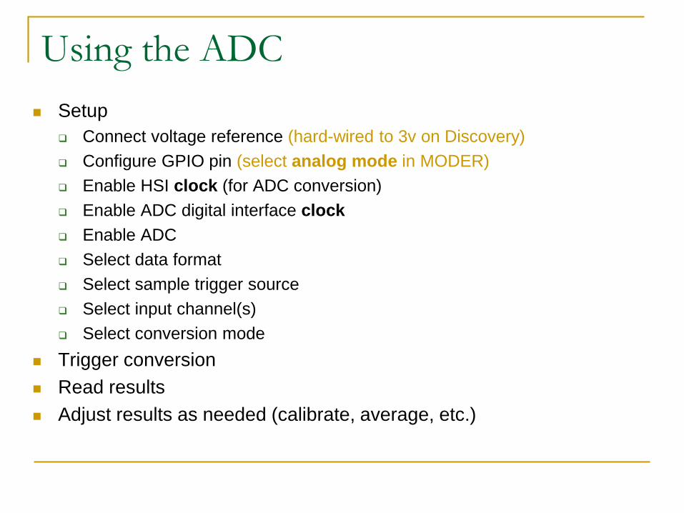
Using the ADC Setup
Connect voltage reference (hard-wired to 3v on Discovery) Configure GPIO pin (select analog mode in MODER) Enable HSI clock (for ADC conversion) Enable ADC digital interface clock Enable ADC Select data format Select sample trigger source Select input channel(s) Select conversion mode
Trigger conversion Read results Adjust results as needed (calibrate, average, etc.)

ADC initialization Configure GPIO pin(s) as analog signals
Refer to Pin Definition Table in STM32L100 data sheet to determine which GPIO pins correspond to ADC_IN0..ADC_IN21 Example: GPIOA pins PA0 - PA7 = ADC_IN0 - ADC_IN7, respectively
Enable GPIOx clock in RCC->AHB1ENR Select analog mode in GPIOx->MODER (disables pull-up/down resistors)
Enable HSI clock in RCC->CR, which runs ADC conversions RCC->CR |= RCC_CR_HSION; //HSION = bit 0 of RCC->CR
Enable ADC1 clock in RCC->APB2ENR (for ADC digital interface) Power up the ADC
Set ADON bit in ADC1->CR2 (control register 2) Wait until ADONS = 1 in ADC1->SR (takes 3.5 - 4 µsec) For power efficiency, shut off the ADC when not used
Configure ADC options (data format, conversion mode, etc.)
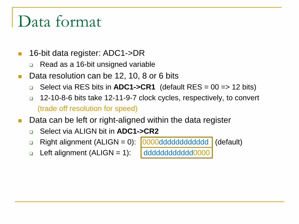
Data format
16-bit data register: ADC1->DR Read as a 16-bit unsigned variable
Data resolution can be 12, 10, 8 or 6 bits Select via RES bits in ADC1->CR1 (default RES = 00 => 12 bits) 12-10-8-6 bits take 12-11-9-7 clock cycles, respectively, to convert
(trade off resolution for speed) Data can be left or right-aligned within the data register
Select via ALIGN bit in ADC1->CR2 Right alignment (ALIGN = 0): 0000dddddddddddd (default) Left alignment (ALIGN = 1): dddddddddddd0000
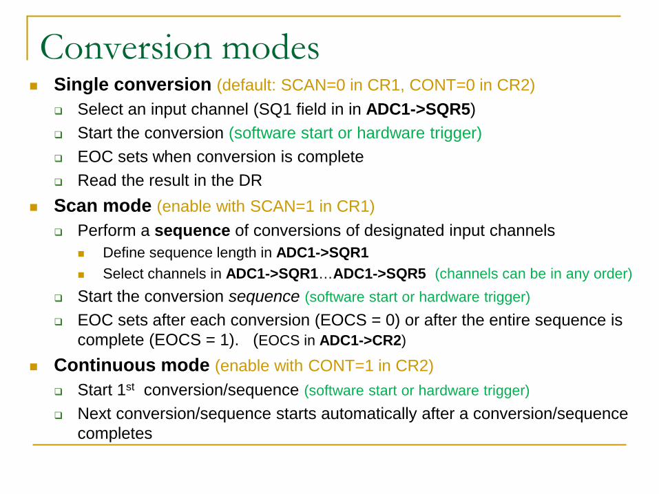
Conversion modes Single conversion (default: SCAN=0 in CR1, CONT=0 in CR2)
Select an input channel (SQ1 field in in ADC1->SQR5) Start the conversion (software start or hardware trigger) EOC sets when conversion is complete Read the result in the DR
Scan mode (enable with SCAN=1 in CR1) Perform a sequence of conversions of designated input channels
Define sequence length in ADC1->SQR1 Select channels in ADC1->SQR1…ADC1->SQR5 (channels can be in any order)
Start the conversion sequence (software start or hardware trigger) EOC sets after each conversion (EOCS = 0) or after the entire sequence is
complete (EOCS = 1). (EOCS in ADC1->CR2)
Continuous mode (enable with CONT=1 in CR2) Start 1st conversion/sequence (software start or hardware trigger) Next conversion/sequence starts automatically after a conversion/sequence
completes

ADC timing
ADC stabilizes
sample + convert End conversion,DR ready
Set in CR2
Turn on ADC in CR2
In SR: ADC ready
Poweron
Datasample

ADC conversion time
Total conversion time = Tsampling + Tconversion Tconversion = 12/11/9/7 cycles for 12/10/8/6 bit resolution Tsampling = sampling time, specified for each channel
Options: 4, 9, 16, 24, 48, 96, 192, 384 clock cycles 3-bit value SMPn[2:0] sets sample time for channel n
ADC1->SMPR3 configures channels 9-0 ADC1->SMPR2 configures channels 19-10 ADC1->SMPR1 configures channels 29-20
Example: Fastest conversion rate for 12-bit datafADCCLK = 16MHz; min Tsampling = 4; max res. = 12 bitsTtotal = (4 + 12)/16MHz = 1us (1 Msamples/sec)

Example: Set Tsampling = 24 clock cycles for ADC_IN8
ADC1->SMPR3 (reset value = 0x00000000)
SMPx[2:0]: Channel x Sample time selection (# clock cycles)000: 4 cycles, 010: 16 cycles, 100: 48 cycles, 110: 192 cycles010: 9 cycles, 011: 24 cycles, 101: 96 cycles, 111: 384 cycles
Default is 4 cycles for each channel
// Set sample time for ADC_IN8 to 24 cyclesADC1->SMPR3 &= ~ADC_SMPR3_SMP8; //Clear SMP8 bits* ADC1->SMPR3 |= 0x03000000; //SMP8 = 3
*ADC_SMPR3_SMP8 = 0x03000000

ADC control register 1 (ADC1->CR1)
RES[1:0]: resolution00: 12-bit, TCONV = 12 cycles01: 10-bit, TCONV = 11 cycles10: 8-bit, TCONV = 9 cycles11: 6-bit, TCONV = 7 cycles
EOCIE: end of conversioninterrupt enable:
0: disable the interrupt1: enable ADC interrupt
when EOC sets
Reset value = 0x0000 0000 (bold values below)
SCAN: enable scan mode0: disable Scan mode1: enable Scan mode
(convert inputs selected in ADC_SQRx)
Default setup:• 12-bit sample• single channel (no scan)• no interrupt

ADC control register 2 (ADC1->CR2)
ADON: Turn ADC on/off0: Disable ADC1: Enable ADC
CONT: 0: single conversion mode1: continuous conversion mode
SWSTART: Software “start” signalWrite 1 to start conversionResets when conversion starts
ALIGN: Data alignment in 16-bit result register0: Right alignment (upper bits = 0)1: Left alignment (lower bits = 0)
EOCS: End of conversion selection0: EOC bit set at end of conversion sequence1: EOC bit set at end of each conversion
Reset value = 0x0000 0000
//Turn on ADCADC1->CR2 |= 1;
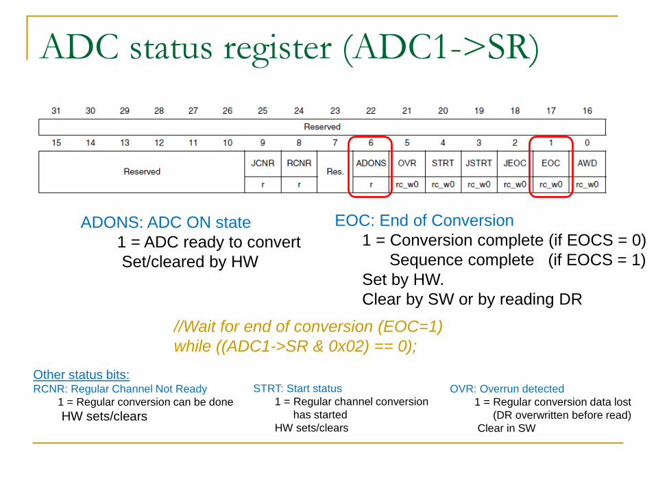
ADC status register (ADC1->SR)
Other status bits:RCNR: Regular Channel Not Ready
1 = Regular conversion can be doneHW sets/clears
EOC: End of Conversion1 = Conversion complete (if EOCS = 0)
Sequence complete (if EOCS = 1)Set by HW. Clear by SW or by reading DR
//Wait for end of conversion (EOC=1)while ((ADC1->SR & 0x02) == 0);
ADONS: ADC ON state1 = ADC ready to convertSet/cleared by HW
STRT: Start status1 = Regular channel conversion
has startedHW sets/clears
OVR: Overrun detected1 = Regular conversion data lost
(DR overwritten before read)Clear in SW
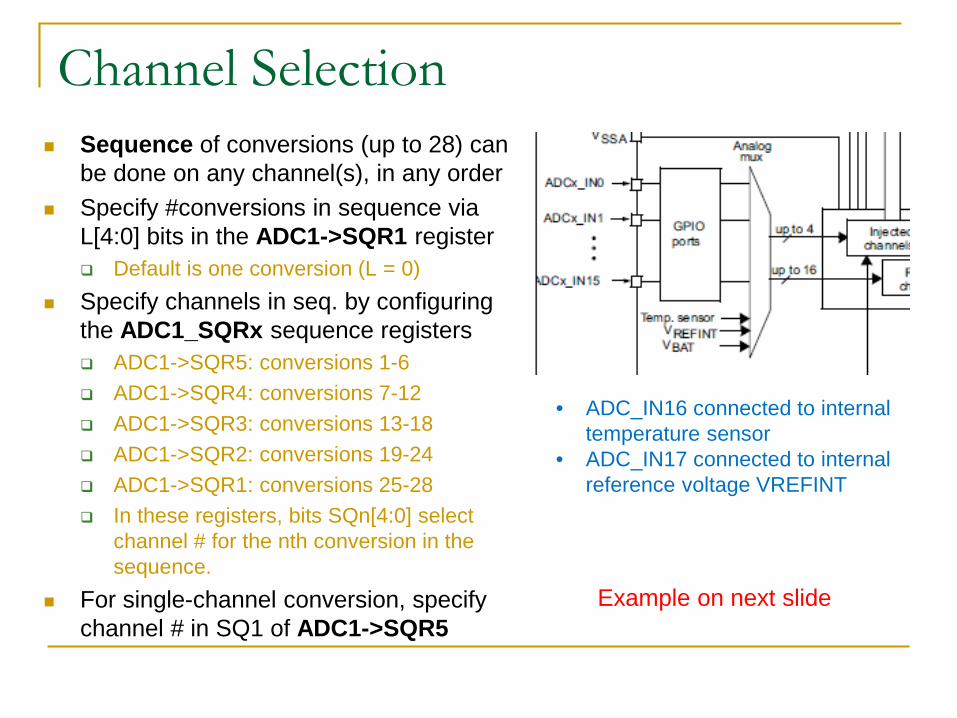
Channel Selection Sequence of conversions (up to 28) can
be done on any channel(s), in any order Specify #conversions in sequence via
L[4:0] bits in the ADC1->SQR1 register Default is one conversion (L = 0)
Specify channels in seq. by configuring the ADC1_SQRx sequence registers ADC1->SQR5: conversions 1-6 ADC1->SQR4: conversions 7-12 ADC1->SQR3: conversions 13-18 ADC1->SQR2: conversions 19-24 ADC1->SQR1: conversions 25-28 In these registers, bits SQn[4:0] select
channel # for the nth conversion in the sequence.
For single-channel conversion, specify channel # in SQ1 of ADC1->SQR5
• ADC_IN16 connected to internal temperature sensor
• ADC_IN17 connected to internal reference voltage VREFINT
Example on next slide
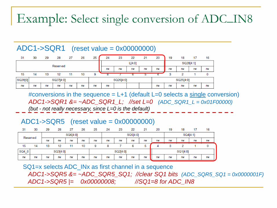
Example: Select single conversion of ADC_IN8
ADC1->SQR1 (reset value = 0x00000000)
#conversions in the sequence = L+1 (default L=0 selects a single conversion)ADC1->SQR1 &= ~ADC_SQR1_L; //set L=0 (ADC_SQR1_L = 0x01F00000)(but - not really necessary, since L=0 is the default)
ADC1->SQR5 (reset value = 0x00000000)
SQ1=x selects ADC_INx as first channel in a sequenceADC1->SQR5 &= ~ADC_SQR5_SQ1; //clear SQ1 bits (ADC_SQR5_SQ1 = 0x0000001F)ADC1->SQR5 |= 0x00000008; //SQ1=8 for ADC_IN8
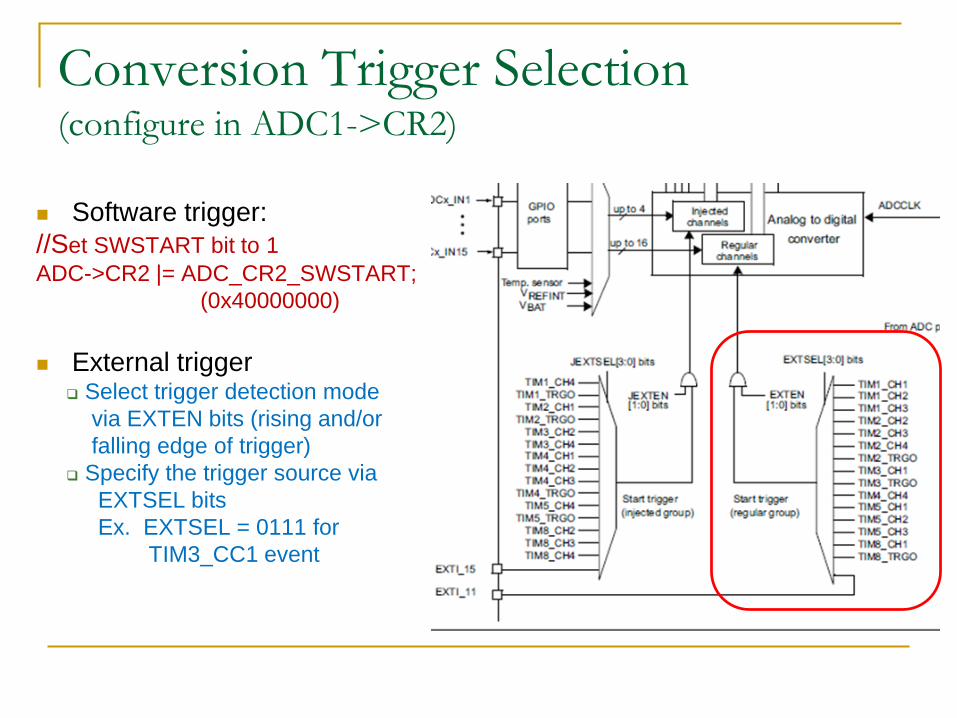
Conversion Trigger Selection(configure in ADC1->CR2)
Software trigger: //Set SWSTART bit to 1ADC->CR2 |= ADC_CR2_SWSTART;
(0x40000000)
External trigger Select trigger detection mode
via EXTEN bits (rising and/or falling edge of trigger)
Specify the trigger source via EXTSEL bitsEx. EXTSEL = 0111 for
TIM3_CC1 event

Using the ADC (summary) Setup
Connect voltage reference (hard-wired to 3v on Discovery) Configure GPIO pin (select analog mode in MODER, turn on GPIO clk) Enable HSI clock for ADC conversion (RCC->CR) Enable ADC digital interface clock (RCC-<APB2ENR) Power on ADC (CR2) Select data format (CR1,CR2) Select conversion mode (CR1,CR2) Select sample time (SMPR3) Select input channel(s) (SQR1,SQR5)
Trigger conversion (Software: CR2, or External: CR2) Read results (DR) Adjust results as needed (calibrate, average, etc.)

Working with ADC data samples
𝐴𝐴𝐴𝐴𝐴𝐴𝐴 → 𝐴𝐴𝐷𝐷 =𝑉𝑉𝑉𝑉𝑉𝑉𝑉𝑉𝑉𝑉𝑉𝑉𝑉𝑉
× 2#𝑏𝑏𝑏𝑏𝑏𝑏𝑏𝑏
Several conversions may be needed Average several samples of N to filter out noise Compute approximate input voltage Vin from N For a sensor, use sensor’s transfer function to compute the physical
parameter value (e.g. pressure) from Vin Do additional computations based on this physical parameter (e.g. compute
depth based on pressure) Convert data to some other form (eg. ASCII characters, to send to a display)
Numeric considerations Consider resolution of measured data (eg. 12 bits) vs resolution of other data
involved in calculations Consider measurement errors in the ADC Some program data may be in floating-point format

Lab Procedure Design and incorporate a rectifier & filter into your circuit to
convert the tachometer output to a DC voltage level Model in PSPICE to verify design. Measure tachometer signal and rectifier/filter output with o’scope. EEBoard waveform generator can be used to test the circuit without
the motor.
Modify software to add ADC initialization function and ADC input function (trigger conversion, wait for EOC, read result) Consider averaging some # of samples EEBoard waveform generator can be used to test the circuit without
the motor.
Measure: tachometer signal amplitude, rectifier/filter voltage output & ADC value for each of the 10 speed settings
Plot: ADC value vs tachometer output amplitude ADC value vs. ATD input voltage (rectifier/filter output) ADC value vs. PWM signal duty cycle