L4: Sequential Building Blocks (Flip-flops, Latches and...
26
L4: 6.111 Spring 2004 1 Introductory Digital Systems Laboratory L4: Sequential Building Blocks L4: Sequential Building Blocks (Flip (Flip - - flops, Latches and Registers) flops, Latches and Registers) (Most) Lecture material derived from R. Katz, “Contemporary Logic Design”, Addison Wesley Publishing Company, Reading, MA, 1993. Some material from J. Rabaey, A. Chandrakasan, B. Nikolic, “Digital Integrated Circuits: A Design Perspective” Prentice Hall, 2003.
Transcript of L4: Sequential Building Blocks (Flip-flops, Latches and...

L4: 6.111 Spring 2004 1Introductory Digital Systems Laboratory
L4: Sequential Building BlocksL4: Sequential Building Blocks
(Flip(Flip--flops, Latches and Registers)flops, Latches and Registers)
(Most) Lecture material derived from R. Katz, “Contemporary Logic Design”, Addison Wesley Publishing Company, Reading, MA, 1993. Some material from J. Rabaey, A. Chandrakasan, B. Nikolic, “Digital Integrated Circuits: A Design Perspective” Prentice Hall, 2003.
L4: 6.111 Spring 2004 2Introductory Digital Systems Laboratory
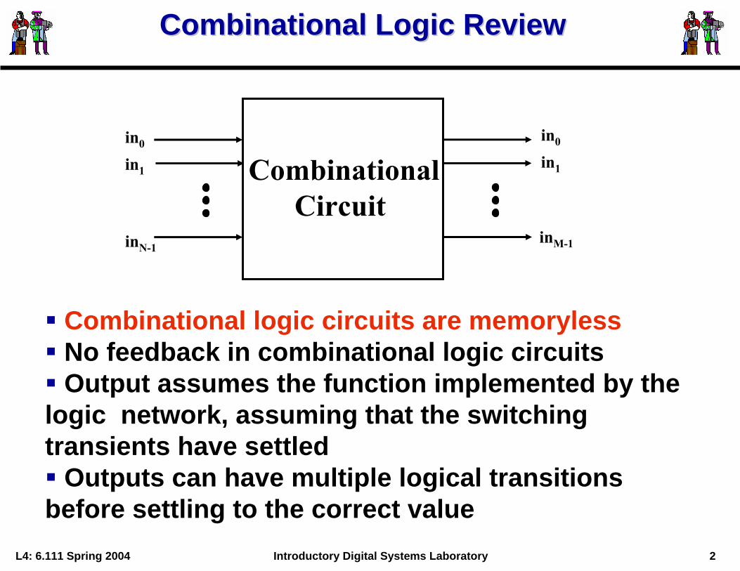
Combinational Logic ReviewCombinational Logic Review
Combinational logic circuits are memorylessNo feedback in combinational logic circuits Output assumes the function implemented by the
logic network, assuming that the switching transients have settled
Outputs can have multiple logical transitions before settling to the correct value
CombinationalCircuit
in0
in1
inN-1
in0
in1
inM-1
L4: 6.111 Spring 2004 3Introductory Digital Systems Laboratory
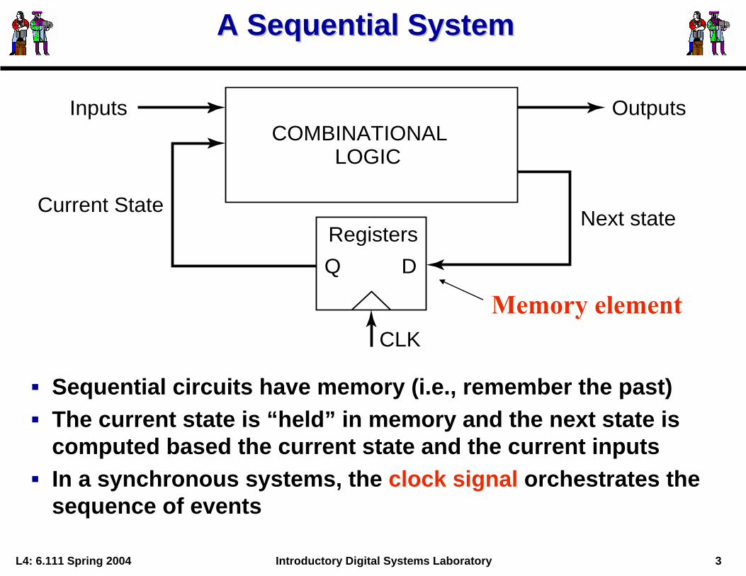
A Sequential SystemA Sequential System
Sequential circuits have memory (i.e., remember the past)The current state is “held” in memory and the next state is computed based the current state and the current inputsIn a synchronous systems, the clock signal orchestrates the sequence of events
COMBINATIONALLOGIC
Registers
Outputs
Next state
CLK
Q D
Current State
Inputs
Memory element
L4: 6.111 Spring 2004 4Introductory Digital Systems Laboratory
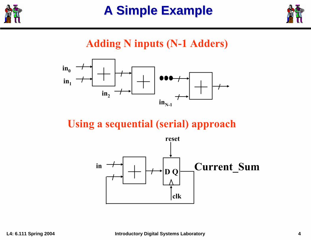
A Simple ExampleA Simple Example
in0
in1
in2inN-1
Adding N inputs (N-1 Adders)
inD Q
reset
clk
Current_Sum
Using a sequential (serial) approach
L4: 6.111 Spring 2004 5Introductory Digital Systems Laboratory
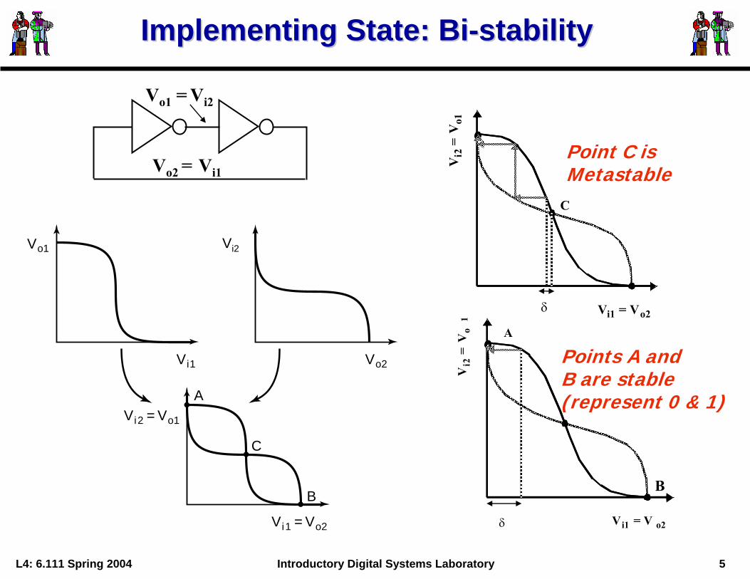
Implementing State: BiImplementing State: Bi--stabilitystability
Vi1
A
C
B
Vo2
Vi1 = Vo2
Vo1 Vi2
Vi2 = Vo1
Vo1 = Vi2
Vo2 = Vi1Point C is Metastable
Vi2
=V
o
Vi1 = V o2
A
δ
Vi2
=V
o 1
Vi1 = Vo2
C
δ
1
Points A andB are stable(represent 0 & 1)
B
L4: 6.111 Spring 2004 6Introductory Digital Systems Laboratory
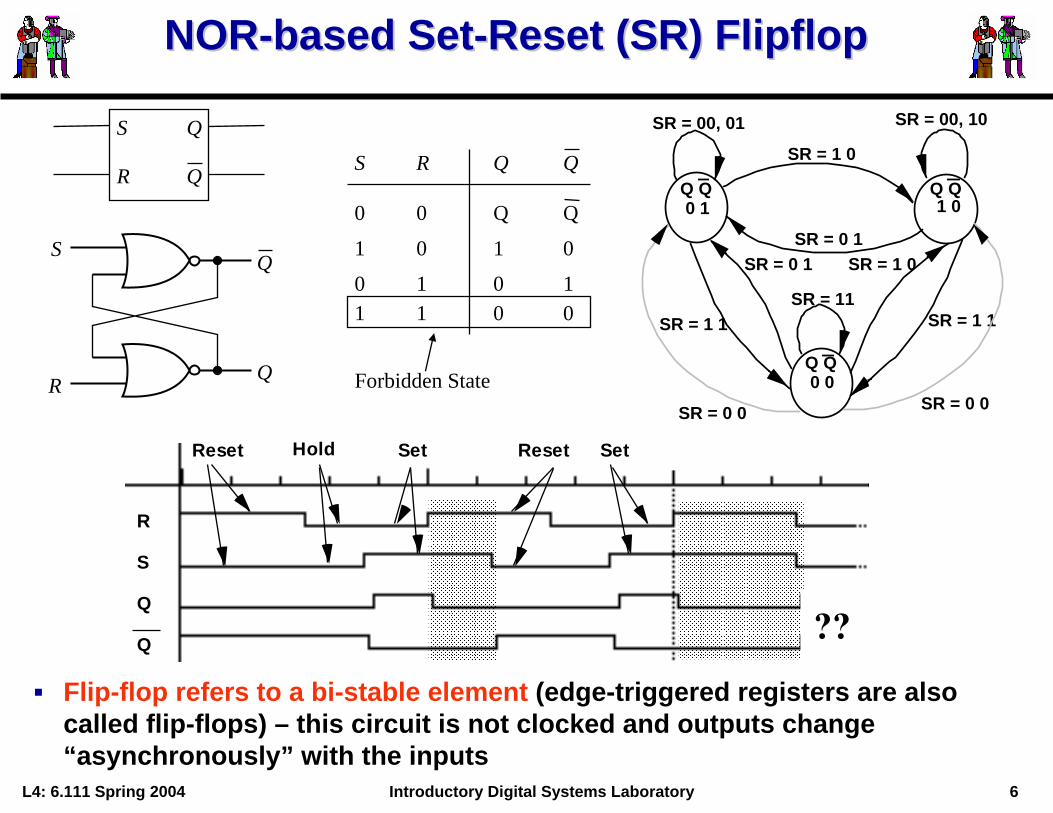
NORNOR--based Setbased Set--Reset (SR) Reset (SR) FlipflopFlipflop
Flip-flop refers to a bi-stable element (edge-triggered registers are also called flip-flops) – this circuit is not clocked and outputs change “asynchronously” with the inputs
Q Q Q Q
Q Q
0 1 1 0
0 0
SR = 1 0
SR = 0 1SR = 0 1
SR = 1 1
SR = 1 0
SR = 1 1
SR = 00, 01 SR = 00, 10
SR = 0 0
SR = 11
SR = 0 0Forbidden State
S
S
R
Q
Q
Q QRS Q
Q00 Q
101 0
010 1011 0
R Q
Reset Hold Set SetReset
R
S
Q
Q??
L4: 6.111 Spring 2004 7Introductory Digital Systems Laboratory
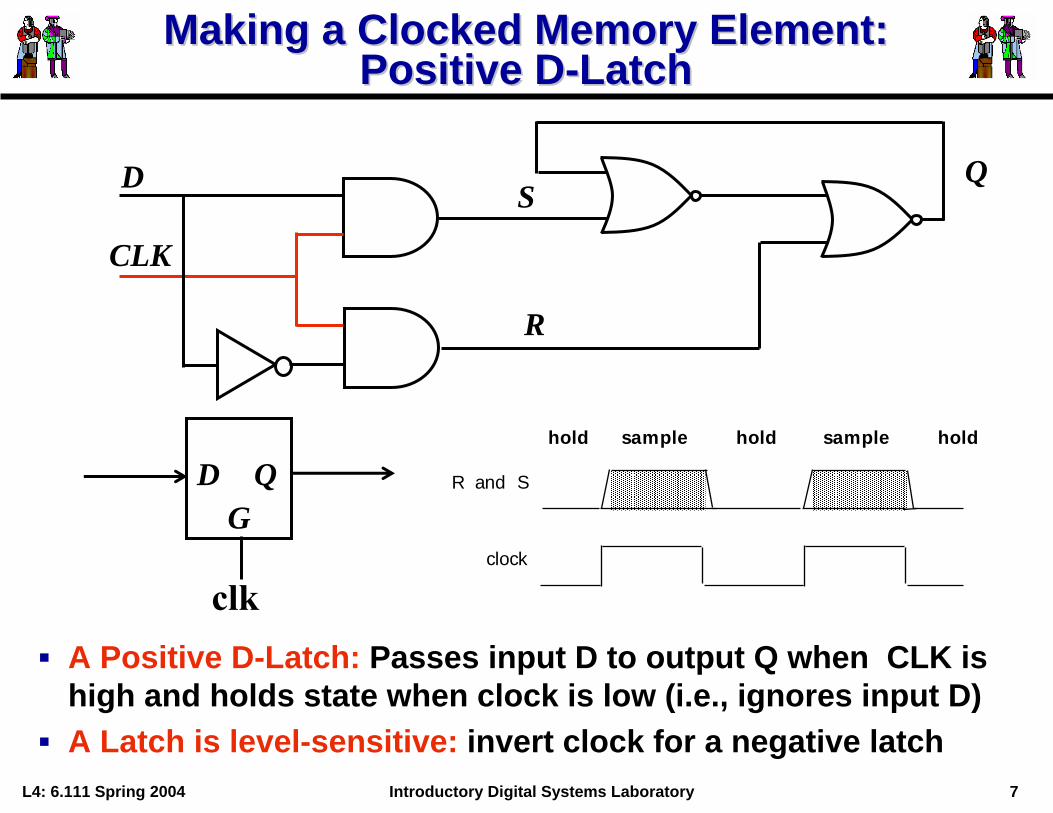
Making a Clocked Memory Element:Making a Clocked Memory Element:Positive DPositive D--LatchLatch
CLK
D Q
D Q
clkA Positive D-Latch: Passes input D to output Q when CLK is high and holds state when clock is low (i.e., ignores input D)A Latch is level-sensitive: invert clock for a negative latch
S
R
clock
R and S
sample hold sample holdhold
G
L4: 6.111 Spring 2004 8Introductory Digital Systems Laboratory
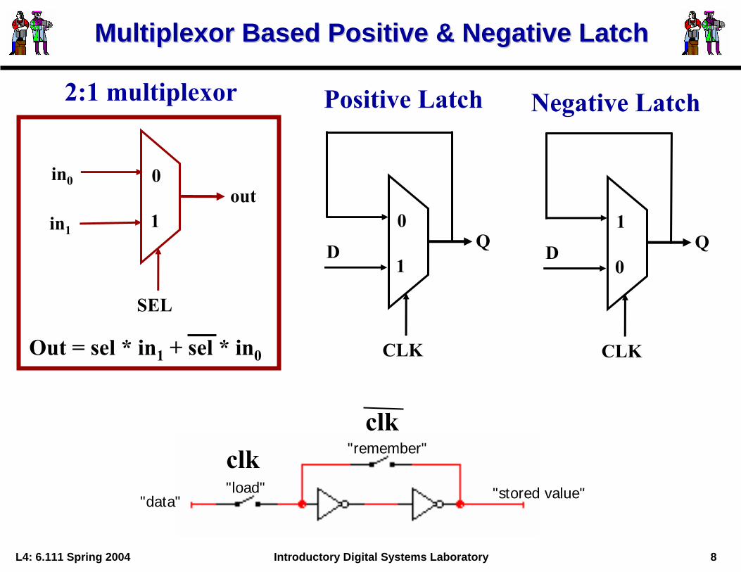
MultiplexorMultiplexor Based Positive & Negative LatchBased Positive & Negative Latch
1
0in0
in1
out
SEL
Out = sel * in1 + sel * in0
2:1 multiplexor
1
0
D Q
CLK
Positive Latch
0
1
D Q
CLK
Negative Latch
"remember"
"load""data" "stored value"
clkclk
L4: 6.111 Spring 2004 9Introductory Digital Systems Laboratory
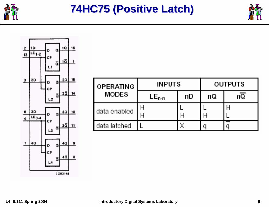
74HC75 (Positive Latch)74HC75 (Positive Latch)
L4: 6.111 Spring 2004 10Introductory Digital Systems Laboratory
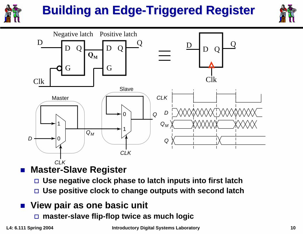
Building an EdgeBuilding an Edge--Triggered RegisterTriggered Register
Master-Slave RegisterUse negative clock phase to latch inputs into first latchUse positive clock to change outputs with second latch
View pair as one basic unitmaster-slave flip-flop twice as much logic
D
G
Q D
G
Q
Clk
DNegative latch Positive latch
1
0D
CLK
QM
Master
0
1
CLK
Q
Slave
QM
Q
D
CLK
QD
Clk
QQD
QM

L4: 6.111 Spring 2004 11Introductory Digital Systems Laboratory
Latches vs. EdgeLatches vs. Edge--Triggered Register Triggered Register
Edge triggered device sample inputs on the event edge
Transparent latches sample inputs as long as the clock is asserted
Timing Diagram:
Behavior the same unless input changes while the clock is high
7474
7475
Bubble herefor negative
edge triggeredregister
Positive edge-triggered register
Level-sensitive latch
D Q
D Q
C
Clk
Clk
D
Clk
Q
Q
7474
7475
L4: 6.111 Spring 2004 12Introductory Digital Systems Laboratory
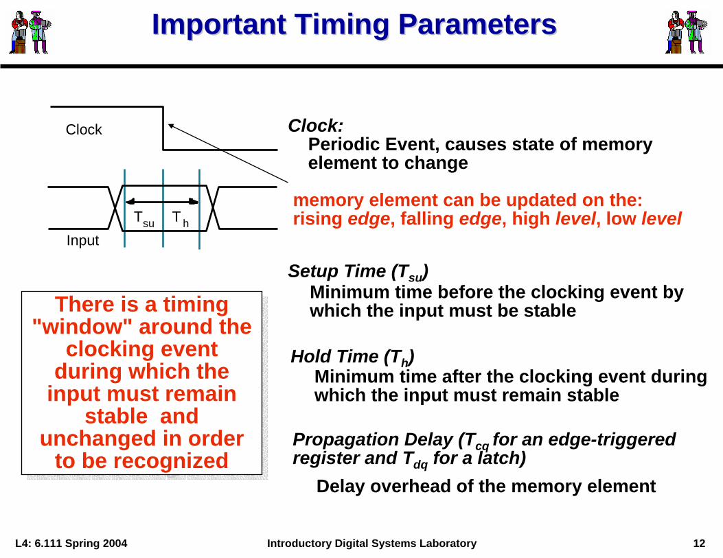
Important Timing ParametersImportant Timing Parameters
Setup Time (Tsu)
Clock: Periodic Event, causes state of memoryelement to change
memory element can be updated on the: rising edge, falling edge, high level, low level
There is a timing "window" around the
clocking event during which the
input must remain stable and
unchanged in order to be recognized
There is a timing "window" around the
clocking event during which the
input must remain stable and
unchanged in order to be recognized
Minimum time before the clocking event by which the input must be stable
Hold Time (Th)Minimum time after the clocking event during which the input must remain stable
Input
Clock
T su T h
Propagation Delay (Tcq for an edge-triggered register and Tdq for a latch)
Delay overhead of the memory element
L4: 6.111 Spring 2004 13Introductory Digital Systems Laboratory
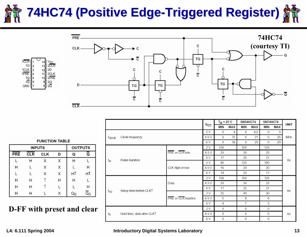
74HC74 (Positive Edge74HC74 (Positive Edge--Triggered Register)Triggered Register)
74HC74(courtesy TI)
D-FF with preset and clear

L4: 6.111 Spring 2004 14Introductory Digital Systems Laboratory
The JThe J--K FlipK Flip--FlopFlop
S
R
Q
Q
J
K
Eliminate the forbidden state of the SR Flip-flopUse output feedback to guarantee that R and S are never both one
1
0
1
0
K
Q
1
0
Q
Q+ Q+J
Q0
10
Q1
01J
K
Q
\ Q
100
L4: 6.111 Spring 2004 15Introductory Digital Systems Laboratory
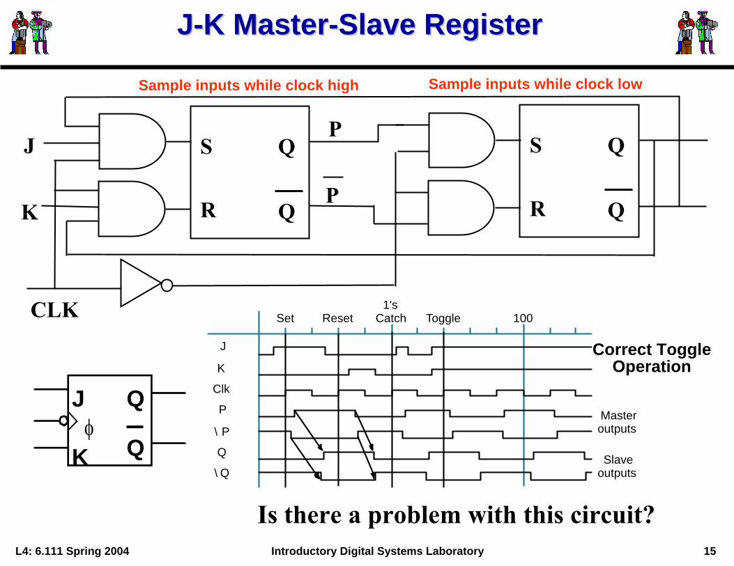
JJ--K MasterK Master--Slave RegisterSlave Register
S
R
Q
Q
J
K
S
R
Q
Q
CLK
Sample inputs while clock high Sample inputs while clock low
Correct ToggleOperation
Master outputs
Slave outputs
Set Reset T oggle 1's
Catch 100
J
K
Clk
P
\ P
Q
\ Q
P
P
J
K
Q
Qφ
Is there a problem with this circuit?
L4: 6.111 Spring 2004 16Introductory Digital Systems Laboratory
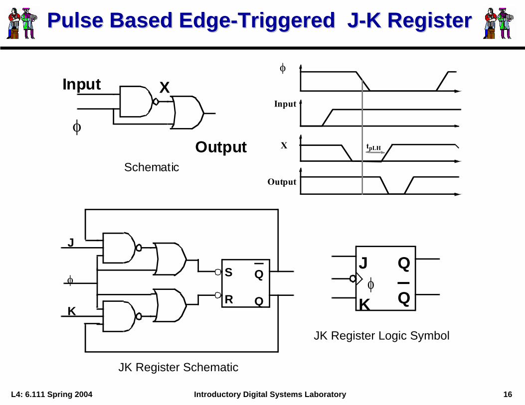
Pulse Based EdgePulse Based Edge--Triggered JTriggered J--K RegisterK Register
S
R
Q
Q
J
K
φJ
K
Q
Qφ
JK Register Schematic
JK Register Logic Symbol
Input
φOutput
Input
X
Output
tpLH
Xφ
Schematic
L4: 6.111 Spring 2004 17Introductory Digital Systems Laboratory
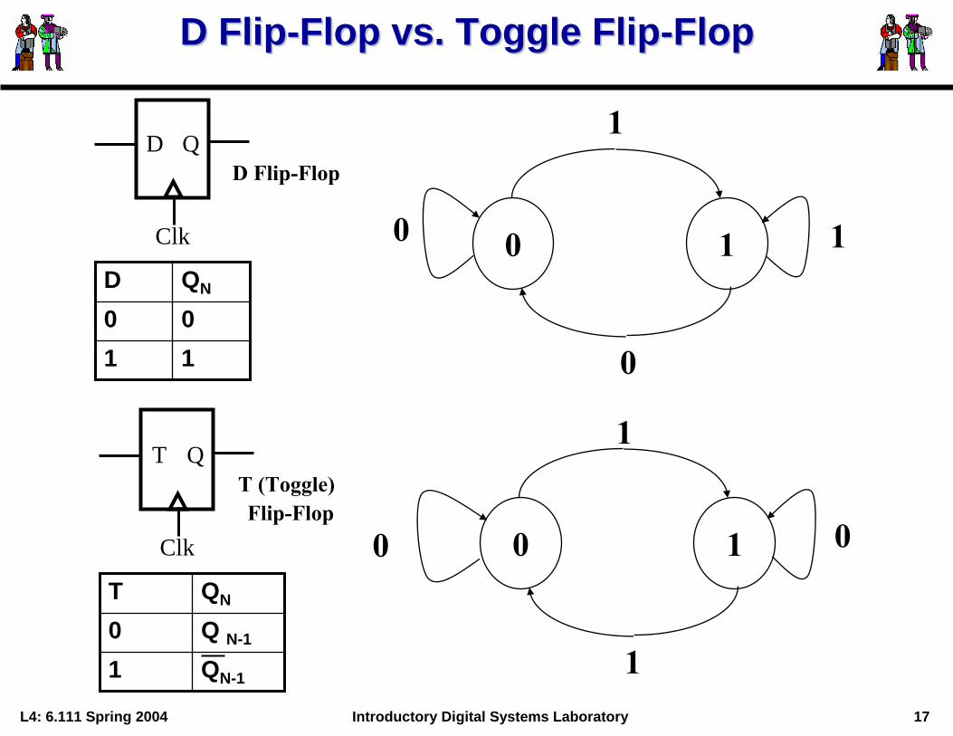
D FlipD Flip--Flop vs. Toggle FlipFlop vs. Toggle Flip--Flop Flop
T
Clk
QT (Toggle)Flip-Flop
0 1
1
1
0
QN-11Q N-10QNT
0
D
Clk
QD Flip-Flop
0 1
0
1
0
1100QND
1

L4: 6.111 Spring 2004 18Introductory Digital Systems Laboratory
Realizing different types of memory elementsRealizing different types of memory elements
Characteristic Equations
D:
J-K:
T:
Q+ = D
Q+ = J Q + K Q
Q+ = T Q + T Q
E.g., J=K=0, then Q+ = QJ=1, K=0, then Q+ = 1J=0, K=1, then Q+ = 0J=1, K=1, then Q+ = Q
Implementing One FF in Terms of Another
D implemented with J-K J-K implemented with D
D J
K J
K C
Q
Q C
D Q
Q
Q

L4: 6.111 Spring 2004 19Introductory Digital Systems Laboratory
Design ProcedureDesign Procedure
Excitation Tables: What are the necessary inputs to cause a particular kind of change in state?
Implementing D FF with a J-K FF:1) Start with K-map of Q+ = ƒ(D, Q)
2) Create K-maps for J and K with same inputs (D, Q)
3) Fill in K-maps with appropriate values for J and K to cause the same state changes as in the original K-map
E.g., D = Q= 0, Q+ = 0then J = 0, K = X
D
0 1
0 1
Q + = D
0 1
0
1
Q
D
X X
1 0
K = D
0 1
0
1
Q D
0 1
X X
J = D
0 1
0
1
Q
D 0 1 0 1
T 0 1 1 0
Q +
0 1 0 1
Q 0 0 1 1
K X X 1 0
J 0 1 X X

L4: 6.111 Spring 2004 20Introductory Digital Systems Laboratory
Design Procedure (cont.)Design Procedure (cont.)
Implementing J-K FF with a D FF:1) K-Map of Q+ = F(J, K, Q)
2,3) Revised K-map using D's excitation tableits the same! that is why design procedure with D FF is simple!
Resulting equation is the combinational logic input to D to cause same behavior as J-K FF. Of course it is identicalto the characteristic equation for a J-K FF.
0 0 1 1
1 0 0 1
00 01 11 10 J
K
JK Q
Q + = D = JQ + KQ
0
1
L4: 6.111 Spring 2004 21Introductory Digital Systems Laboratory
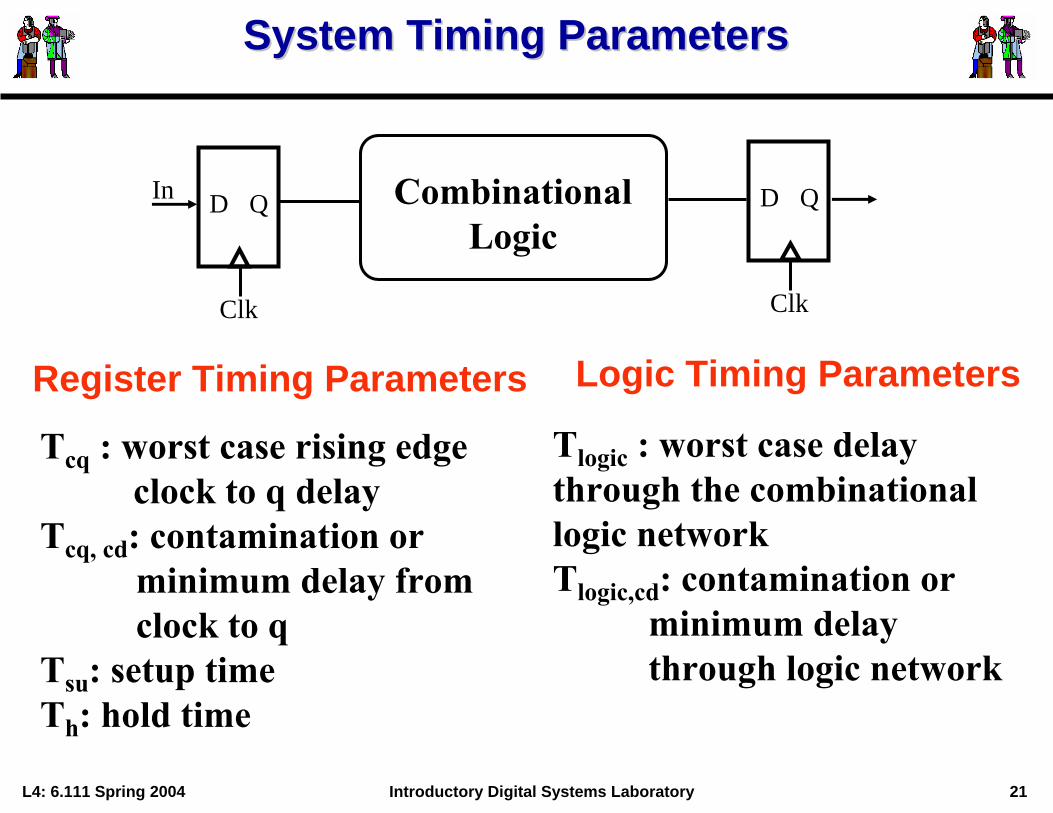
System Timing ParametersSystem Timing Parameters
D
Clk
QIn CombinationalLogic
D
Clk
Q
Register Timing Parameters
Tcq : worst case rising edge clock to q delay
Tcq, cd: contamination or minimum delay from clock to q
Tsu: setup timeTh: hold time
Logic Timing Parameters
Tlogic : worst case delay through the combinational logic networkTlogic,cd: contamination or
minimum delay through logic network
L4: 6.111 Spring 2004 22Introductory Digital Systems Laboratory
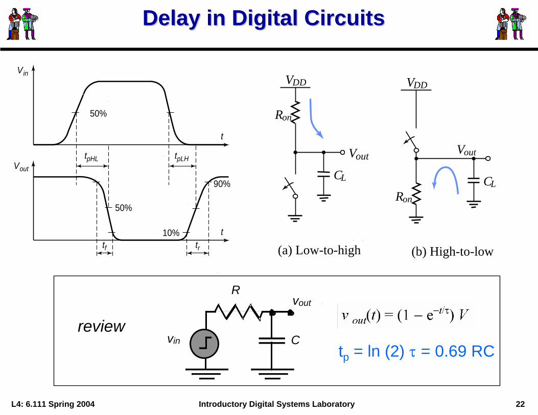
Delay in Digital CircuitsDelay in Digital Circuits
Vout
tf
tpHL tpLH
trt
Vin
t
90%
10%
50%
50%
VoutVout
Ron
Ron
VDDVDD
(a) Low-to-high (b) High-to-low
CLCL
vout
vin C
R
tp = ln (2) τ = 0.69 RCreview

L4: 6.111 Spring 2004 23Introductory Digital Systems Laboratory
System Timing (I): Minimum PeriodSystem Timing (I): Minimum Period
D
Clk
QInCL D
Clk
Q
CLK
Tsu
Th
Tsu
Th
Tcq
Tcq,cd
Tcq
Tcq,cd
FF1
IN
CLoutTl,cd
Tsu2
Tlogic
T > Tcq + Tlogic + Tsu

L4: 6.111 Spring 2004 24Introductory Digital Systems Laboratory
System Timing (II): Minimum DelaySystem Timing (II): Minimum Delay
D
Clk
QIn CombinationalLogic
D
Clk
Q
CLK
Tsu
Th Th
Tcq,cd
FF1
IN
CLoutTl,cd
Tcq,cd + Tlogic,cd > Thold
CLout

L4: 6.111 Spring 2004 25Introductory Digital Systems Laboratory
ShiftShift--RegisterRegister
all measurements are made from the clocking event that is,
the rising edge of the clock
Typical parameters for Positive edge-triggered D Register
Th5ns
Tw 25ns
Tplh25ns13ns
Tphl40ns25ns
Tsu20ns
D
CLK
Q
Tsu20ns
Th5ns
IN
Q0
Q1
CLK
100
CLK
INQ0 Q1
DQ DQ OUT
Shift-register

L4: 6.111 Spring 2004 26Introductory Digital Systems Laboratory
Clocks are not perfect: Clocks are not perfect: Clock SkewClock Skew
D
Clk
QIn CombinationalLogic
D
ClkD
Q
Wire delay
CLK
CLKD
δ>0
CLout
Tcq + Tlogic + Tsu - δT >
Tcq,cd + Tlogic,cd > Thold + δ