KS8993 Jan05 - ww1.microchip.com
35
April 2009 1 KS8993 KS8993 Micrel KS8993 3-Port 10/100 Integrated Switch with PHY and Frame Buffer Rev. 2.06 General Description The KS8993 contains three 10/100 physical layer transceiv- ers, three MAC (Media Access Control) units with an inte- grated layer 2 switch. The device runs in two modes. The first mode is a three port integrated switch and the second is as a three port switch with the third port decoupled from the physical port. In this mode access to the third MAC is provided using a reverse or forward MII (Media Independent Interface) such that an external MAC can be directly connected to the KS8993. This interface also supports the 7-wire (serial net- work interface) as used by some routing devices. Useful configurations include a stand alone three port switch as well as a two port switch with a routing element connected to the extra MII port. The additional port is also useful for public network interfacing. Micrel, Inc. • 2180 Fortune Drive • San Jose, CA 95131 • USA • tel + 1 (408) 944-0800 • fax + 1 (408) 474-1000 • http://www.micrel.com Functional Diagram Look-Up Engine (1K Entries) SRAM Buffers (16Kx32) MII / SNI (exclusive) External Interface FIFO and Flow Control Queue Management Buffer Management LED and Programming Interface MRXD[3:0] MRXDV MCOL MTXD[3:0] MTXEN MTXER Physical Transceiver 1 MAC 1 RXP[1], RXM[1] TXP[1], TXM[1] Physical Transceiver 2 MAC 2 RXP[2], RXM[2] TXP[2], TXM[2] Physical Transceiver 3 MAC 3 RXP[3], RXM[3] TXP[3], TXM[3] LED[1][3:0] LED[2][3:0] LED[3][3:0] MRXD[0] MRXDV MCOL MTXD[0] MTXEN S N I M I I MTXCLK MRXCLK MTXCLK MCOLIN MCRS MRXCLK The KS8993 has rich features such as VLAN and priority queuing and is designed to reside in an unmanaged design not requiring processor intervention. This is achieved through I/O strapping at system reset time. On the media side, the KS8993 supports 10BaseT, 100BaseTX and 100BaseFX as specified by the IEEE 802.3 committee. Physical signal transmission and reception are enhanced through use of analog circuitry that makes the design more efficient and allows for lower power consumption and smaller chip die size. Data sheets and support documentation can be found on Micrel’s web site at www.micrel.com.
Transcript of KS8993 Jan05 - ww1.microchip.com

April 2009 1 KS8993
KS8993 Micrel
KS89933-Port 10/100 Integrated Switch with PHY and Frame Buffer
Rev. 2.06
General DescriptionThe KS8993 contains three 10/100 physical layer transceiv-ers, three MAC (Media Access Control) units with an inte-grated layer 2 switch. The device runs in two modes. The firstmode is a three port integrated switch and the second is asa three port switch with the third port decoupled from thephysical port. In this mode access to the third MAC is providedusing a reverse or forward MII (Media Independent Interface)such that an external MAC can be directly connected to theKS8993. This interface also supports the 7-wire (serial net-work interface) as used by some routing devices.
Useful configurations include a stand alone three port switchas well as a two port switch with a routing element connectedto the extra MII port. The additional port is also useful forpublic network interfacing.
Micrel, Inc. • 2180 Fortune Drive • San Jose, CA 95131 • USA • tel + 1 (408) 944-0800 • fax + 1 (408) 474-1000 • http://www.micrel.com
Functional Diagram
Look-UpEngine
(1K Entries)
SRAMBuffers
(16Kx32)
MII / SNI(exclusive)ExternalInterface
FIFO and Flow Control
QueueManagement
BufferManagement
LEDand
ProgrammingInterface
MRXD[3:0]MRXDVMCOL
MTXD[3:0]MTXENMTXER
PhysicalTransceiver
1
MAC1
RX
P[1]
, RX
M[1
]
TX
P[1]
, TX
M[1
]
PhysicalTransceiver
2
MAC2
RX
P[2]
, RX
M[2
]
TX
P[2]
, TX
M[2
]
PhysicalTransceiver
3
MAC3
RX
P[3]
, RX
M[3
]
TX
P[3]
, TX
M[3
]
LED[1][3:0]LED[2][3:0]LED[3][3:0]
MRXD[0]MRXDVMCOL
MTXD[0]MTXEN
SNI
MII
MTXCLK
MRXCLK
MTXCLKMCOLIN
MCRSMRXCLK
The KS8993 has rich features such as VLAN and priorityqueuing and is designed to reside in an unmanaged designnot requiring processor intervention. This is achieved throughI/O strapping at system reset time.
On the media side, the KS8993 supports 10BaseT,100BaseTX and 100BaseFX as specified by the IEEE 802.3committee.
Physical signal transmission and reception are enhancedthrough use of analog circuitry that makes the design moreefficient and allows for lower power consumption and smallerchip die size.
Data sheets and support documentation can be found onMicrel’s web site at www.micrel.com.

KS8993 Micrel
KS8993 2 April 2009
Ordering Information
Part Number TemperatureStandard Pb-Free Range Package
KS8993 KSZ8993 0°C to +70°C 128-Pin PQFP
Features• 3-port 10/100 integrated switch with physical layer
transceivers• 64k Byte of SRAM on chip for frame buffering• 1.0Gbps high performance memory bandwidth• 10BaseT, 100BaseTX and 100BaseFX modes of
operation• Support for UTP or fiber installations• Superior analog technology for reduced power and die
size• Supports port based VLAN• QoS feature!! Supports 802.1p based priority or port-
based priority• Indicators for link, activity, full/half-duplex and speed• Unmanaged operation via strapping at system reset
time• Hardware based 10/100, full/half, flow control and auto-
negotiation• Individual port forced modes (full-duplex, 100BaseTX)
when auto-negotiation is disabled• Wire speed reception and transmission• On chip integrated address look-up engine, supports 1K
absolute MAC addresses• Automatic address learning, address aging and address
migration• Full-duplex IEEE 802.3x flow control (Pause) with force
mode option• Half-duplex back pressure flow control• Comprehensive LED support• External MAC interface (MII or SNI 7-wire ) for router
applications• 300mA (0.75W) including physical transmit drivers• Commercial temperature range: 0°C to +70°C• Available in 128-pin PQFP with single 2.5V power
supply

April 2009 3 KS8993
KS8993 Micrel
Revision HistoryRevision Date Summary of Changes
1.00 04/13/00 Document origination
1.01 05/31/00 Miscellaneous changes
1.02 06/08/00 Index repair
1.03 09/20/00 MII forward correction.MRXD[3:1] correction.
1.04 10/30/00 Update voltage ratings.
1.05 10/31/00 Correct I/O descriptions.
1.06 11/08/00 Correct mode operation for LED[1:3][0]Add timing information
1.07 12/21/00 Correct pin information
1.08 03/23/01 Correct VLAN description.
1.09 03/26/01 Update MODESEL descriptions for packet size extensions
1.10 04/19/01 Update electrical characteristics; Correct I/O information.
1.11 04/20/01 Correct timing information
1.12 05/10/01 Update I/O descriptions
1.13 06/08/01 Define control for LED[3][3]
1.14 06/26/01 Revise definition for LED[3][3]
1.15 08/1/01 Update timing information and power dissipationAdd power up timing description; Correct DISAN3 default mode.
1.16 08/9/01 Correct LED [1] [1] to float configurationAdd Reverse and Forward MII timing
2.00 4/8/02 Correct reserve buffer from 128 to 96 for PRSV pin.Add max. current.Add force flow control Option as follows:Change pin 50 from reserved to FFLOW1# for force flow control on port 1.)Change pin 46 from reserved to FFLOW2# for force flow control on port 2.Modify LED[1][2] for force flow control on port 3.
2.01 5/6/02 Add TX Disable for Port 1 and port 2, Power down for port 3 and Far end Fault Disable features usingMUX[1:2] and TEST[1:2] pins.
2.02 7/2/02 Recommend pull-down on LED[3][3]
2.03 8/29/03 Convert to new format.
2.04 1/24/05 Added reset circuit recommendation.
2.05 5/12/05 Added lead-free part number

KS8993 Micrel
KS8993 4 April 2009
Table of ContentsSystem Level Applications .............................................................................................................................................................. 5
Pin Description .............................................................................................................................................................................. 6
I/O Grouping .............................................................................................................................................................................. 9
I/O Descriptions ............................................................................................................................................................................ 10
Pin Configuration ........................................................................................................................................................................... 15
Functional Overview: Physical Layer Transceiver ..................................................................................................................... 16
100BaseTX Transmit ............................................................................................................................................................... 16
100BaseTX Receive ................................................................................................................................................................ 16
PLL Clock Synthesizer ............................................................................................................................................................ 16
Scrambler/De-scrambler (100BaseTX only) ............................................................................................................................ 16
100BaseFX operation .............................................................................................................................................................. 16
100BaseFX Signal Detection ................................................................................................................................................... 16
100BaseFX Far End Fault ....................................................................................................................................................... 16
10BaseT Transmit ................................................................................................................................................................... 16
10BaseT Receive .................................................................................................................................................................... 16
Power Management ................................................................................................................................................................ 17
LED Mode Selection ................................................................................................................................................................ 17
Auto-Negotiation ...................................................................................................................................................................... 17
Functional Overview: Switch Core ............................................................................................................................................... 18
Address Look Up ..................................................................................................................................................................... 18
Learning .......................................................................................................................................................................... 18
Migration ......................................................................................................................................................................... 18
Aging ............................................................................................................................................................................ 18
Forwarding ...................................................................................................................................................................... 18
Switching Engine ..................................................................................................................................................................... 18
MAC (Media Access Controller) Operation ............................................................................................................................. 18
Inter Packet Group .......................................................................................................................................................... 18
Back off Algorithm ........................................................................................................................................................... 18
Late Collision .................................................................................................................................................................. 18
Illegal Frame ................................................................................................................................................................... 18
Flow Control .................................................................................................................................................................... 18
Full-Duplex Flow Control ................................................................................................................................................. 18
Half-Duplex Back Pressure ............................................................................................................................................. 18
VLAN Support .......................................................................................................................................................................... 19
QoS Priority Support ................................................................................................................................................................ 20
MII Interface Operation .................................................................................................................................................................. 21
SNI Interface (7-wire) Operation ................................................................................................................................................... 22
Absolute Maximum Ratings .......................................................................................................................................................... 23
Operating Ratings .......................................................................................................................................................................... 23
Electrical Characteristics .............................................................................................................................................................. 23
Timing Diagrams ............................................................................................................................................................................ 24
Reference Circuit ........................................................................................................................................................................... 29
4B/5B Coding ............................................................................................................................................................................ 31
MLT Coding ............................................................................................................................................................................ 32
802.1q VLAN and 802.1p Priority Frame ...................................................................................................................................... 33
Selection of Isolation Transformers ............................................................................................................................................. 34
Selection of Reference Crystals ................................................................................................................................................... 34
Package Outline and Dimensions ................................................................................................................................................ 35

April 2009 5 KS8993
KS8993 Micrel
System Level ApplicationsThe KS8993 can be configured to fit either in a three port 10/100 application or as a two port 10/100 network interface withan extra MII or SNI port. This MII/SNI port can be connectedto an external processor and used for routing purposes or
public network access. The major benefits of using theKS8993 are the lower power consumption, unmanaged op-eration, flexible configuration and built in frame buffering.Two such applications are depicted below.
KS89933-PortSwitch
withPHY
KS89933-PortSwitchwithPHY
RoutingEngine
3XTransformer
or FiberInterface
2XTransformer
or FiberInterface
PublicNetworkAccess
3-Port Stand Alone 2-Port with PublicNetwork InterfaceOr
Figure 1. KS8993 Applications

KS8993 Micrel
KS8993 6 April 2009
Pin DescriptionPin Number Pin Name Type(Note 1) Port Pin Function
1 GND_ANA GND Analog ground
2 MUX[2] I Factory test pin
3 MUX[1] I Factory test pin
4 GND_RX[1] GND 1 Ground for receiver
5 RXP[1] I 1 Physical receive signal + (differential)
6 RXM[1] I 1 Physical receive signal - (differential)
7 VDD_RX[1] Pwr 1 2.5V for receiver
8 VREF[1] O 1 Reference voltage for transmit transformer center tap
9 TXP[1] O 1 Physical transmit signal + (differential)
10 TXM[1] O 1 Physical transmit signal - (differential)
11 GND_TX[1] GND 1 Ground for transmit circuitry
12 VDD_TX[1] Pwr 1 2.5V for transmit circuitry
13 VDD_BG Pwr 2.5V for analog circuitry
14 ISET O Set physical transmit output current
15 GND_BG GND Ground for analog circuitry
16 GND_PLL GND Ground for phase locked loop circuitry
17 VDD_PLL Pwr 2.5V for phase locked loop circuitry
18 GND_RX[2] GND 2 Ground for receiver
19 RXP[2] I 2 Physical receive signal + (differential)
20 RXM[2] I 2 Physical receive signal - (differential)
21 VDD_RX[2] Pwr 2 2.5V for receiver
22 VREF[2] O 2 Reference voltage for transmit transformer center tap
23 TXP[2] O 2 Physical transmit signal + (differential)
24 TXM[2] O 2 Physical transmit signal - (differential)
25 GND_TX[2] GND 2 Ground for transmit circuitry
26 VDD_TX[2] Pwr 2 2.5V for transmit circuitry
27 VDD_TX[3] Pwr 3 2.5V for transmit circuitry
28 GND_TX[3] GND 3 Ground for transmit circuitry
29 TXP[3] O 3 Physical transmit signal + (differential)
30 TXM[3] O 3 Physical transmit signal - (differential)
31 VREF[3] O 3 Reference voltage for transmit transformer center tap
32 VDD_RX[3] Pwr 3 2.5V for receiver
33 RXP[3] I 3 Physical receive signal + (differential)
34 RXM[3] I 3 Physical receive signal - (differential)
35 GND_RX[3] GND 3 Ground for receiver
36 FXSD[2] I 2 Fiber signal detect
37 FXSD[3] I 3 Fiber signal detect
38 GND_ANA GND Analog ground
Note 1. Pwr = power supply
GND = ground
I = input
O = output
I/O = bi-directional

April 2009 7 KS8993
KS8993 Micrel
Pin Number Pin Name Type(Note 1) Port Pin Function
39 TEST[1] I Factory test pin
40 TEST[2] I Factory test pin
41 GND_RCV[2] GND 2 Ground for clock recovery circuitry
42 VDD_RCV[2] Pwr 2 2.5V for clock recovery circuitry
43 GND_RCV[3] GND 3 Ground for clock recovery circuitry
44 VDD_RCV[3] P 3 2.5V for clock recovery circuitry
45 VMDIS I DIScard VLAN Mismatch packets
46 FFLOW2# I 2 Force flow control on port 2
47 PV32 I 3 Port 3 VLAN Port mask bit 1
48 PV31 I 3 Port 3 VLAN Port mask bit 0
49 PV23 I 2 Port 2 VLAN Port mask bit 2
50 FFLOW1# I 1 Force flow control on port 1
51 PV21 I 2 Port 2 VLAN Port mask bit 0
52 PV13 I 1 Port 1 VLAN Port mask bit 2
53 PV12 I 1 Port 1 VLAN Port mask bit 1
54 DISAN3 I 3 Port 3 auto-negotiation disable (pull this down to enable port 3 autonegotiation)
55 VDD Pwr 2.5V for core digital circuitry
56 GND GND Ground for digital circuitry
57 MTXEN I 3 MII transmit enable
58 MTXD[3] I 3 MII transmit bit 3
59 MTXD[2] I 3 MII transmit bit 2
60 MTXD[1] I 3 MII transmit bit 1
61 MTXD[0] I 3 MII transmit bit 0
62 MTXER I 3 MII transmit error
63 MTXCLK I/O 3 MII output clock
64 MRXDV O 3 MII receive data valid
65 MRXD[3] O 3 MII receive bit 3
66 MRXD[2] O 3 MII receive bit 2
67 MRXD[1] O 3 MII receive bit 1
68 MRXD[0] O 3 MII receive bit 0
69 VDD_IO Pwr 2.5V or 3.3V for MII interface, LEDs and other digital I/O
70 GND GND Ground for digital circuitry
71 MRXCLK I/O 3 MII input clock
72 MCOL O 3 MII collision detect output
73 MCRS I/O 3 MII carrier sense
74 MCOLIN I 3 MII collision detect input
75 MIIS[1] I 3 MII mode select bit 1
76 MIIS[0] I 3 MII mode select bit 0
Note 1. Pwr = power supply
GND = ground
I = input
O = output
I/O = bi-directional

KS8993 Micrel
KS8993 8 April 2009
Pin Number Pin Name Type(Note 1) Port Pin Function
77 MODESEL[3] I Selects LED and test modes
78 MODESEL[2] I Selects LED and test modes
79 MODESEL[1] I Selects LED and test modes
80 MODESEL[0] I Selects LED and test modes
81 TESTEN I Factory test pin - tie low for normal operation
82 SCANEN I Factory test pin - tie low for normal operation
83 RST# I Reset
84 VDD Pwr 2.5V for core digital circuitry
85 GND GND Ground for digital circuitry
86 LED[1][3] O 1 Port 1 LED indicator 3
87 LED[1][2] O 1 Port 1 LED indicator 2
88 LED[1][1] O 1 Port 1 LED indicator 1
89 LED[1][0] O 1 Port 1 LED indicator 0
90 LED[2][3] O 2 Port 2 LED indicator 3
91 LED[2][2] O 2 Port 2 LED indicator 2
92 LED[2][1] O 2 Port 2 LED indicator 1
93 LED[2][0] O 2 Port 2 LED indicator 0
94 VDD_IO Pwr 2.5V or 3.3V for MII interface, LEDs and other digital I/O
95 GND GND Ground for digital circuitry
96 LED[3][3] O 3 Port 3 LED indicator 3
97 LED[3][2] O 3 Port 3 LED indicator 2
98 LED[3][1] O 3 Port 3 LED indicator 1
99 LED[3][0] O 3 Port 3 LED indicator 0
100 PRSV I Priority queue buffer reserve
101 PRSEL[1] I Priority scheme select bit 1
102 PRSEL[0] I Priority scheme select bit 0
103 PBASE2 I Priority base value bit 2
104 PBASE1 I Priority base value bit 1
105 PBASE0 I Priority base value bit 0
106 P3_1PEN I 3 Port 3 802.1p receive priority classification enable
107 P2_1PEN I 2 Port 2 802.1p receive priority classification enable
108 P1_1PEN I 1 Port 1 802.1p receive priority classification enable
109 P3_TXQ2 I 3 Port 3 transmit queue split, priority queueing enable
110 P2_TXQ2 I 2 Port 2 transmit queue split, priority queueing enable
111 P1_TXQ2 I 1 Port 1 transmit queue split, priority queueing enable
112 GND GND Ground for digital circuitry
113 VDD Pwr 2.5V for core digital circuitry
114 P3_PP I 3 Port 3 receive port based priority classification
115 P2_PP I 2 Port 2 receive port based priority classification
Note 1. Pwr = power supply
GND = ground
I = input
O = output
I/O = bi-directional
April 2009 9 KS8993
KS8993 Micrel
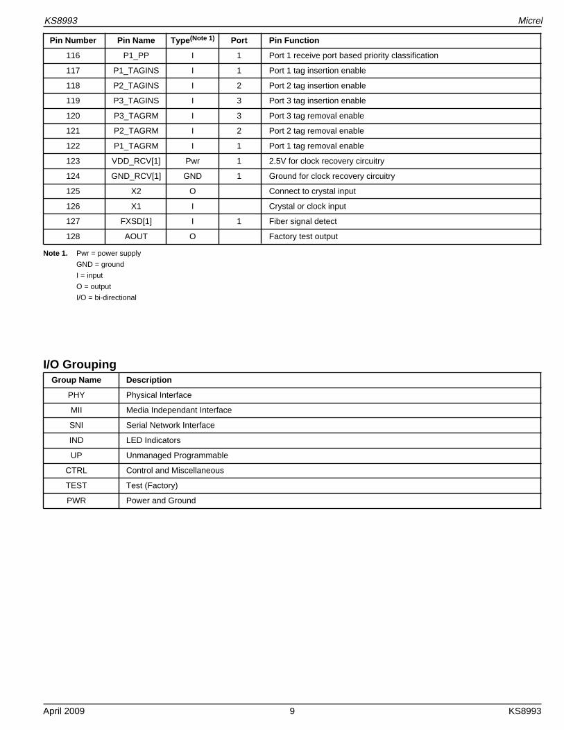
Pin Number Pin Name Type(Note 1) Port Pin Function
116 P1_PP I 1 Port 1 receive port based priority classification
117 P1_TAGINS I 1 Port 1 tag insertion enable
118 P2_TAGINS I 2 Port 2 tag insertion enable
119 P3_TAGINS I 3 Port 3 tag insertion enable
120 P3_TAGRM I 3 Port 3 tag removal enable
121 P2_TAGRM I 2 Port 2 tag removal enable
122 P1_TAGRM I 1 Port 1 tag removal enable
123 VDD_RCV[1] Pwr 1 2.5V for clock recovery circuitry
124 GND_RCV[1] GND 1 Ground for clock recovery circuitry
125 X2 O Connect to crystal input
126 X1 I Crystal or clock input
127 FXSD[1] I 1 Fiber signal detect
128 AOUT O Factory test output
Note 1. Pwr = power supply
GND = ground
I = input
O = output
I/O = bi-directional
I/O GroupingGroup Name Description
PHY Physical Interface
MII Media Independant Interface
SNI Serial Network Interface
IND LED Indicators
UP Unmanaged Programmable
CTRL Control and Miscellaneous
TEST Test (Factory)
PWR Power and Ground

KS8993 Micrel
KS8993 10 April 2009
I/O DescriptionsGroup I/O Names Active Status Description
PHY RXP[1:3] Analog Differential inputs (receive) for connection to media (transformer or fiber module).RXM[1:3]
TXP[1:3] Analog Differential outputs (transmit) for connection to media (transformer or fiber module).TXM[1:3]
FXSD[1:3] H Fiber signal detect - connect to fiber signal detect output on fiber module. Tie lowfor 100TX mode.
VREF[1:3] Analog Center tap transformer reference for transmit data.
ISET Analog Transmit Current Set. Connecting an external reference resistor to set transmitteroutput current. This pin connects a 1% 3kΩ resistor if a transformer of turns ratio of1:1 is used.
MII See “Table 2, MII Interconnect” for forward and reverse signal usage.
MRXD[0:3] H Four bit wide data bus for receiving MAC frames.
MRXDV H Receive data valid.
MCRS H Receive carrier sense.
MCOL H Receive collision detection.
MCOLIN H Collision in (for forward operation only).
MRXCLK Clock Receive clock.
MTXD[0:3] H Four bit wide data bus for transmitting MAC frames.
MTXEN H Transmit enable.
MTXER H Transmit error.
MTXCLK Clock Transmit clock.
SNI MTXD[0] H Serial transmit data.
MTXEN H Transmit enable.
MTXCLK Clock Transmit clock.
MRXD[0] H Serial receive data.
MRXDV H Receive carrier sense/data valid.
MCOL H Collision detection.
MRXCLK Clock Receive clock.
IND LED[1:3][0] L Output (after reset).Mode 0: Speed (low = 100/high = 10).Mode 1: Reserved.Mode 2: Collision (toggle = collision during receiving , high = no collision).Mode 3: Speed (low = 100/high = 10).
LED[1:3][1] L Output (after reset).Mode 0: Duplex (low = full/high = half).Mode 1: Duplex (low = full/high = half).Mode 2: Duplex (low = full/high = half).Mode 3: Reserved.
LED[1:3][2] L Output (after reset).Mode 0: Collision (toggle = collision during receiving , high = no collision).Mode 1: Transmit Activity (toggle during transmission, high = idle).Mode 2: 10/link/act (constant low = link, toggle = act, constant high = no link).Mode 3: Full-Duplex + Collision (constant low = full-duplex, toggle = collision in half.duplex, constant high = half-duplex with no collision).

April 2009 11 KS8993
KS8993 Micrel
Group I/O Names Active Status Description
LED[1:3][3] L Output (after reset).Mode 0: Link + Activity (toggle = receiving or transmitting, constant low = link,constant high = no link).Mode 1: Receive Activity (toggle during receiving / high = no receiving activity).Mode 2: 100/link/act (constant low = link, toggle = act, constant high = no link).Mode 3: Mode 3: Link + Activity (toggle = receiving or transmitting, constant low =link, constant high = no link).Note: Mode is set by MODESEL[3:0] ; please see description in UP “UnmanagedProgramming” section.
UP MODESEL[3:0] H Mode select at reset time. LED mode is selected by using the table below. MODESELalso controls the maximum frame length accepted.
MODESEL
3 2 1 0 LED mode Max Length (no tag/tag)
0 0 0 0 LED mode 0 1518/1522
0 0 0 1 LED mode 1 1518/1522
0 0 1 0 LED mode 2 1518/1522
0 0 1 1 LED mode 3 1518/1522
0 1 0 0 Factory testing Not applicable
0 1 0 1 Factory testing Not applicable
0 1 1 0 Factory testing Not applicable
0 1 1 1 Factory testing Not applicable
1 0 0 0 Factory testing Not applicable
1 0 0 1 Factory testing Not applicable
1 0 1 0 Factory testing Not applicable
1 0 1 1 LED mode 3 1536/1536
1 1 0 0 LED mode 0 1536/1536
1 1 0 1 Factory testing Not applicable
1 1 1 0 LED mode 2 1536 / 1536
1 1 1 1 Factory testing Not applicable
FFLOW1# L Enable force flow control feature on port 1.Pulled up = no force flow control feature on port 1 (default).Flow control feature is enabled and disabled by auto-negotiation.Pulled down = enable force flow control feature on port 1 regardless of auto-negotia-tion result.
FFLOW2# L Program force flow control feature on port 2.Pulled up = no force flow control feature on port 2 (default).Flow control feature is enabled and disabled by auto-negotiation.Pulled down = enable force flow control feature on port 2 regardless of auto-negotia-tion result.
LED[1][3] Program advertise flow control feature for 10/100BaseTX ports during auto-negotia-tion at reset time.Pulled low = no advertise flow control during auto-negotiation.Pulled high = advertise flow control during auto-negotiation (default).
LED[1][2] Programs force flow control feature on port 3, incuding MII port at reset time.Pulled low = no force flow control feature on port 3, including MII port (default).Flow control feature is enabled/disabled by auto-negotiation result.Pulled high = enable force flow control feature on port 3, including MII port regardlessof auto-negotiation result.
LED[1][1] Reserved - use float configuration.

KS8993 Micrel
KS8993 12 April 2009
Group I/O Names Active Status Description
LED[1][0] Programs buffer allocation per port at reset time. Use the following table to select theoption.Pulled low = 170 buffers (default).Pulled high = adaptive mode.
LED[2][3] Programs MAC address aging in the address look-up table at reset time. Agingeliminates old entries from the table.Pulled high = 5 minute aging (default).Pulled low = disable.
LED[2][2] Programs back pressure enable at reset time.Pulled high = enable (default).Pulled low = disable.
LED[2][1] Programs aggressive back off in half-duplex at reset time.Pulled high = enable (default).Pulled low = disable.
LED[2][0] Programs no excessive collision drop at reset time.Pulled high = enable (default).Pulled low = disable.
LED[3][3] RESERVED.Use external pulldown resistor if VDD_IO is 3.3V and LED[3][3] is being used. IfVDD_IO is not 3.3V or this LED is not used, then no pull-down is required ( floating).
LED[3][2:0] Programs force 100BaseTX mode at reset time. Use the table below to set this modeon the appropriate port. Assuming the corresponding port auto-negotiation is disabled.
Signal Port Force 10BaseTX Force 100BaseTX
LED[3][2] 3 Pulled low Pulled high (default)
LED[3][1] 2 Pulled low Pulled high (default)
LED[3][0] 1 Pulled low Pulled high (default)
MRXD[3:1] Programs force full-duplex mode at reset time. Use the table below to set this modeon the appropriate port. Assuming the corresponding port auto-negotiation is disabled.
Signal Port Force Half-Duplex Force Full-Duplex
MRXD[3] 3 Pulled low (default) Pulled high
MRXD[2] 2 Pulled low (default) Pulled high
MRXD[1] 1 Pulled low (default) Pulled high
MRXD0 Programs “port 1 auto-negotiation disable” at reset time.Pulled high = auto-negotiation disable.Pulled low = auto-negotiation enable (default).
MCOL Programs “port 2 auto-negotiation disable” at reset time.Pulled high = auto-negotiation disable.Pulled low = auto-negotiation enable (default).
DISAN3 Programs “port 3 auto-negotiation disable” at reset time.Pulled high = auto-negotiation disable (default)Pulled low = auto-negotiation enable
MIIS[1:0] H Selects external MII port operation mode. Use the table below to select the externalport mode.
MIIS
1 0 Selection
L L External MII disable (default)
L H MII reverse mode
H L MII forward mode
H H 7-wire (SNI) mode

April 2009 13 KS8993
KS8993 Micrel
Group I/O Names Active Status Description
VMDIS H VLAN Mismatch Discard control.Pulled low = Constrict multicast and broadcast packets to VLAN.Pulled high = Constrict all packets to VLAN (default).
PRSV H Reserve priority buffers.Pulled low = No buffers reserved (default).Pulled high = Reserve 96 buffers per port for high priority queue.
PBASE[2:0] H Priority base value used to compare with priority tag in 802.1p tag. When a packet isreceived that has a 802.1p tag and 802.1p processing is enabled (Px_1PEN=H), thePBASE value is compared to the tag priority field. If the packet tag is greater than orequal to the PBASE value, the packet is sent to the higher priority transmit queuewhile tags less than PBASE are sent to the lower priority queue. (default = 100).
PV12 H VLAN mask bits. Used to select which ports are seen from any particular port. UsePV13 the table below to select VLAN operation.PV21 P1_V defined as (PV13, PV12, 1)PV23 P2_V defined as (PV23, 1 , PV21)PV31 P3_V defined as (1 , PV32, PV31)PV32
P[3:1]_VPort 2 1 0 VLAN State
1 0 1 1 Ports 1 and 2 in VLAN1 0 1 Ports 1 and 3 in VLAN1 1 1 Ports 1, 2 and 3 in VLAN (default)
2 0 1 1 Ports 1 and 2 in VLAN1 1 0 Ports 2 and 3 in VLAN1 1 1 Ports 1, 2 and 3 in VLAN (default)
3 1 0 1 Ports 1 and 3 in VLAN1 1 0 Ports 2 and 3 in VLAN1 1 1 Ports 1, 2 and 3 in VLAN (default)
Note that a minimum of 2 ports are required for each VLAN. The VLAN configurationis viewed from the receiver perspective. All states not listed above are invalid.
P[3:1]_1PEN H Enables 802.1p prioritizing on a per port basis. The enable is from the receiveperspective. If the 802.1p processing is disabled or there is no tag, priority is dete-mined by the P[3:1]_PP bit.Pulled low = Disable 802.1p prioritizing (default).Pulled high = Enable 802.1p prioritizing.
P[3:1]_PP H Selects port receive priority in the absence of 802.1p handling.Pulled low = Low priority (default).Pulled high = High priority.
P[3:1]_TAGINS H Inserts 802.1p tag in received packets if not already existent. The priority field is setbased on the port P[3:1]_PP bit. For the P[3:1]_PP bit tied low, the priority field is setto 000 and for the P[3:1]_PP bit tied high, the priority field is set to 111.Pulled low = No change to received packet (default).Pulled high = Insert 802.1p tag.
Note that if P[3:1]_TAGINS and P[3:1]_TAGRM are both set for the same port, thereis no change to the packet.
P[3:1]_TAGRM H Removes 802.1p tag in received packets if they exist.Pulled low = No change to received packet (default).Pulled high = Remove 802.1p tag.
Note that if P[3:1]_TAGINS and P[3:1]_TAGRM are both set for the same port, thereis no change to the packet.
P[3:1]_TXQ2 H Selects transmit queue split on a per port basis. The split sets up high and low priorityqueues.Pulled low = Single transmit queue (default)Pulled high = Separate high and low transmit queues

KS8993 Micrel
KS8993 14 April 2009
Group I/O Names Active Status Description
PRSEL[1:0] H Selects queue servicing if using split transmit queues. Use the table below to selectdesired servicing. Note that this selection effects all split transmit queue ports in thesame way.
PRSEL1 0 Priority Selection
L L Transmit all high priority before low priority (default)
L H Transmit high priority at 10:1 ratio
H L Transmit high priority at 5:1 ratio
H H Transmit high priority at 2:1 ratio
CTRL X1 Clock External crystal or clock input
X2 Clock Used when other polarity of crystal is needed. This is unused for a normal clock input.
RST# L System reset
TEST TESTEN H Factory test input - pull low
SCANEN H Factory test input - pull low
AOUT H Factory test output - leave open
MUX[1:2] H Mux[1] Mux[2]
Float Float Default for factory test purpose
1 Float TX Disable Port 1
0 Float TX Disable Port 2
Float 1 Power Down Port 3
Special note: all other combinations are not allowed
TEST[1:2] H Test[1] Test[2]
Float Float Default for factory test purpose
Float 0 Far End Fault Disable
Special note: all other combinations are not allowed .
PWR VDD_RX[1:3] 2.5V for receiver
GND_RX[1:3] Ground for receiver
VDD_TX[1:3] 2.5V for transmit circuitry
GND_TX[1:3] Ground for transmit circuitry
VDD_RCV[1:3] 2.5V for clock recovery circuitry
GND_RCV[1:3] Ground for clock recovery
VDD_PLL 2.5V for phase locked loop circuitry
GND_PLL Ground for phase locked loop circuitry
GND_ANA Analog ground
GND_BG Analog ground
VDD_BG 2.5V for analog circuits
VDD 2.5V for core digital circuitry
VDD_IO 2.5V or 3.3V for MII interface, LEDs and other digital I/O
GND Ground for digital circuitry

April 2009 15 KS8993
KS8993 Micrel
Pin Configuration
65
391
103
PR
SE
L[0]
PR
SE
L[1]
PR
SV
LED
[3][0
]LE
D[3
][1]
LED
[3][2
]LE
D[3
][3]
GN
DV
DD
_IO
LED
[2][0
]LE
D[2
][1]
LED
[2][2
]LE
D[2
][3]
LED
[1][0
]LE
D[1
][1]
LED
[1][2
]LE
D[1
][3]
GN
DV
DD
RS
T#
SC
AN
EN
TE
ST
EN
MO
DE
SE
L[0]
MO
DE
SE
L[1]
MO
DE
SE
L[2]
MO
DE
SE
L[3]
MIIS
[0]
MIIS
[1]
MC
OLI
NM
CR
SM
CO
LM
RX
CLK
GN
DV
DD
_IO
MR
XD
[0]
MR
XD
[1]
MR
XD
[2]
MR
XD
[3]
GN
D_A
NA
MU
X[2
]M
UX
[1]
GN
D_R
X[1
]R
XP
[1]
RX
M[1
]V
DD
_RX
[1]
VR
EF
[1]
TX
P[1
]T
XM
[1]
GN
D_T
X[1
]V
DD
_TX
[1]
VD
D_B
GIS
ET
GN
D_B
GG
ND
_PLL
VD
D_P
LLG
ND
_RX
[2]
RX
P[2
]R
XM
[2]
VD
D_R
X[2
]V
RE
F[2
]T
XP
[2]
TX
M[2
]G
ND
_TX
[2]
VD
D_T
X[2
]V
DD
_TX
[3]
VD
D_T
X[3
]T
XP
[3]
TX
M[3
]V
RE
F[3
]V
DD
_RX
[3]
RX
P[3
]R
XM
[3]
GN
D_R
X[3
]F
XS
D[2
]F
XS
D[3
]G
ND
_AN
A
MRXDVMTXCLKMTXERMTXD[0]MTXD[1]MTXD[2]MTXD[3]MTXENGNDVDDDISAN3PV12PV13PV21FFLOW1#PV23PV31PV32FFLOW2#VMDISVDD_RCV[3]GND_RCV[3]VDD_RCV[2]GND_RCV[2]TEST[2]TEST[1]
PBASE2PBASE1PBASE0
P3_1PENP2_1PENP1_1PENP3_TXQ2P2_TXQ2P1_TXQ2
GNDVDD
P3_PPP2_PPP1_PP
P1_TAGINSP2_TAGINSP3_TAGINSP3_TAGRMP2_TAGRMP1_TAGRM
VDD_RCV[1]GND_RCV[1]
X2X1
FXSD[1]AOUT
128-Pin PQFP (PQ)

KS8993 Micrel
KS8993 16 April 2009
Functional Overview: Physical Layer Transceiver100BaseTX TransmitThe 100BaseTX transmit function performs parallel to serial conversion, 4B/5B coding, scrambling, NRZ to NRZI conversion,MLT3 encoding and transmission. The circuit starts with a parallel to serial conversion, which converts the data from the MACinto a 125MHz serial bit stream. The data and control stream is then converted into 4B/5B coding followed by a scrambler. Theserialized data is further converted from NRZ to NRZI format, then transmitted in MLT3 current output. The output current isset by an external 1% 3.01kΩ resistor for the 1:1 transformer ratio. It has a typical rise/fall time of 4ns and complies to the ANSITP-PMD standard regarding amplitude balance, overshoot and timing jitters.
100BaseTX ReceiveThe 100BaseTX receiver function performs adaptive equalization, DC restoration, MLT3 to NRZI conversion, data and clockrecovery, NRZI to NRZ conversion, de-scrambling, 4B/5B decoding and serial to parallel conversion. The receiving side startswith the equalization filter to compensate inter-symbol interference (ISI) over the twisted pair cable. Since the amplitude lossand phase distortion is a function of the length of the cable, the equalizer has to adjust its characteristics to optimize theperformance. In this design, the variable equalizer will make an initial estimation based on comparisons of incoming signalstrength against some known cable characteristics, then tunes itself for optimization. This is an ongoing process and can selfadjust against the environmental changes such as temperature variations.
The equalized signal then goes through a DC restoration and data conversion block. The DC restoration circuit is used tocompensate for the effect of base line wander and improve the dynamic range. The differential data conversion circuit convertsthe MLT3 format back to NRZI. The slicing threshold is also adaptive.
The clock recovery circuit extracts the 125MHz clock from the edges of the NRZI signal. This recovered clock is then used toconvert the NRZI signal into the NRZ format. The signal is then sent through the de-scrambler followed by the 4B/5B decoder.Finally, the NRZ serial data is provided as the input data to the MAC.
PLL Clock SynthesizerThe KS8993 generates clocks for the external MII and SNI interface based on the interface type selected.
Scrambler/De-scrambler (100BaseTX only)The purpose of the scrambler is to spread the power spectrum of the signal in order to reduce EMI and baseline wander. Thedata is scrambled by the use of an 11-bit wide linear feedback shift register (LFSR). This can generate a 2047-bit non-repetitivesequence. The receiver will then de-scramble the incoming data stream with the same sequence at the transmitter.
100BaseFX Operation100BaseFX operation is very similar to 100BaseTX operation with the differences being that the scrambler/de-scrambler andMLT3 encoder/decoder are bypassed on transmission and reception. In this mode the auto-negotiation feature is bypassedsince there is no standard that supports fiber auto-negotiation.
100BaseFX Signal DetectionThe physical port runs in 100BaseFX mode if FXSDx >.6V. This signal is referenced to VREFx which is set at 1/2 Vdd but canbe overridden by an external level. VREFx can be connected to the “minus” signal of a differential pair coming from the fibermodule (“plus connects to FXSDx) used to convey signal detect. When FXSDx is below .6V then 100BaseFX mode is disabled.
100BaseFX Far End FaultFar end fault occurs when the signal detection is logically false from the receive fiber module. When this occurs, thetransmission side signals the other end of the link by sending 84 1’s followed by a zero in the idle period between frames.
Far End Fault can be disabled by setting external hardware pin TEST[2]=0 and TEST[1] = float. See “I/O Description” for pindescription.
10BaseT TransmitThe output 10BaseT driver is incorporated into the 100BaseT driver to allow transmission with the same magnetic. They areinternally wave-shaped and pre-emphasized into outputs with a typical 2.2V amplitude. The harmonic contents are at least27dB below the fundamental when driven by an all-ones Manchester-encoded signal.
Special note for 10BaseT operation: With an operating voltage of 2.5V, the KS8993 does not always achieve the specifiedtransmit voltage swing greater than or equal to 2.2V as specified by IEEE 802.3. The important factor however is that theKS8993 does adhere to the specified receive signal voltages using the IEEE twisted pair model with a 100Ω load. The transmitvoltage swing can be increased to 2.2V or above by increasing the supply voltage to 2.65V if so desired.
10BaseT ReceiveOn the receive side, input buffer and level detecting squelch circuits are employed. A differential input receiver circuit and aPLL perform the decoding function. The Manchester-encoded data stream is separated into clock signal and NRZ data. A

April 2009 17 KS8993
KS8993 Micrel
squelch circuit rejects signals with levels less than 400mV or with short pulse widths in order to prevent noises at the RXP orRXM input from falsely triggering the decoder. When the input exceeds the squelch limit, the PLL locks onto the incoming signaland the KS8993 decodes a data frame. The receiver clock is maintained active during idle periods in between data reception.
Power ManagementPower Save ModeThe KS8993 will turn off everything except for the Energy Detect and PLL circuits when the cable is not installed on an individualport basis. In other words, the KS8993 will shutdown most of the internal circuits to save power if there is no link.
An additional features are available:
Transmit Disable for Port 1 set external pin MUX[1] = 1 and MUX[2] = Float
Transmit Disable for Port 2 set external pin MUX[1] = 0 and MUX[2] = Float
Power Down on Port 3 set external pin MUX[1] = float and MUX[2] = 1
See “I/O Description” section for pin description.
LED Mode SelectionUse the following table as a quick reference for setting the LED mode. See MODESEL “I/O Description” section forMODESEL[3:2] usage.
MODESEL[1:0] LED[1:3]3 LED[1:3]2 LED[1:3]1 LED[1:3]0
00 Link + Act Collision FDX Speed
01 RX Act TX Act FDX Reserved
10 100 / Link / Act 10 / Link / Act FDX Collision
11 Link + Act FDX + Collision Reserved Speed
Table 1. LED Mode Selection
Auto-NegotiationThe KS8993 conforms to the auto-negotiation protocol as described by the 802.3 committee. Auto-negotiation allows UTP(Unshielded Twisted Pair) link partners to select the best common mode of operation. In auto-negotiation the link partnersadvertise capabilities across the link to each other. If auto-negotiation is not supported or the link partner to the KS8993 is forcedto bypass auto-negotiation, then the mode is set by observing the signal at the receiver. This is known as parallel mode becausewhile the transmitter is sending auto-negotiation advertisements, the receiver is listening for advertisements or a fixed signalprotocol.
The flow for the link set up is depicted below.
StartAuto-Negotiation
Force Link Setting
Listen for10BaseT Link
Pulses
Listen for 100BaseTX
Idles
Attempt Auto-Negotiation
Link Mode Set
BypassAuto-Negotiation
and Set Link Mode
Link Mode Set ?
ParallelOperation
Join Flow
No
Yes
Yes
No
Figure 2. Auto-Negotiation

KS8993 Micrel
KS8993 18 April 2009
Functional Overview: Switch CoreAddress Look-UpThe internal look-up table stores MAC addresses and their associated information. It contains 1K full CAM with 48-bit addressplus switching information. The KS8993 is guaranteed to learn 1K addresses and distinguishes itself from hash-based look-up tables which, depending on the operating environment and probabilities, may not guarantee the absolute number ofaddresses it can learn.
LearningThe internal look-up engine will update its table with a new entry if the following conditions are met:
• The received packet’s SA does not exist in the look-up table.
• The received packet is good; the packet has no receiving errors, and is of legal length.
The look-up engine will insert the qualified SA into the table, along with the port number, time stamp. If the table is full, thelast entry of the table will be deleted first to make room for the new entry.
MigrationThe internal look-up engine also monitors whether a station is moved. If it happens, it will update the table accordingly.Migration happens when the following conditions are met:
• The received packet’s SA is in the table but the associated source port information is different.
• The received packet is good; the packet has no receiving errors, and is of legal length.
The look-up engine will update the existing record in the table with the new source port information.
AgingThe look-up engine will update time stamp information of a record whenever the corresponding SA appears. The time stampis used in the aging process. If a record is not updated for a period of time, the look-up engine will then remove the record fromthe table. The look-up engine constantly performs the aging process and will continuously remove aging records. The agingperiod is approximately 300 seconds ±75 sec. This feature can be enabled or disabled by external pull-up or pull-down resistors.If aging is disabled and look-up table is full, KS8993 will remove the largest address in the table which has been sorted bythe binary search.
ForwardingThe KS8993 will forward packets as follows:
• If the DA look-up results is a “match”, the KS8993 will use the destination port information to determine where thepacket goes.
• If the DA look-up result is a “miss”, the KS8993 will forward the packet to all other ports except the port that receivedthe packet.
• All the multicast and broadcast packets will be forwarded to all other ports except the source port.
The KS8993 will not forward the following packets:
• Error packets. These include framing errors, FCS errors, alignment errors, and illegal size packet errors.
• 802.3x pause frames. The KS8993 will intercept these packets and do the appropriate actions.
• “Local” packets. Based on destination address (DA) look-up. If the destination port from the look-up table matchesthe port where the packet was from, the packet is defined as “local”.
Switching EngineThe KS8993 has a very high performance switching engine to move data to and from the MAC’s, packet buffers. It operatesin store and forward mode, while the efficient switching mechanism reduces overall latency.
The KS8993 has an internal buffer for frames that is 16kx32 (64kB). This resource is shared between the three ports. Buffersizing per port can be programmed at system reset time by using the unmanaged program mode (I/O strapping).
Each buffer is sized at 128B and therefore there are a total of 512 buffers available. A per port maximum can be set at 170buffers (equal allocation). There is also an adaptive mode that reacts to port traffic. In the adaptive mode any given port mayuse up to 256 buffers provided that the other ports are lightly loaded. In the event of heavier loading on other ports the limitis 170 buffers.
MAC (Media Access Controller) OperationThe KS8993 strictly abides by IEEE 802.3 standard to maximize compatibility and interoperability with other vendors.
Inter Packet Gap (IPG)If a frame is successfully transmitted, the 96 bit time IPG is measured between the two consecutive MTXEN. If the currentpacket is experiencing collision, the 96 bit time IPG is measured from MCRS and the next MTXEN.

April 2009 19 KS8993
KS8993 Micrel
Back off AlgorithmThe KS8993 implements the IEEE Std 802.3 binary exponential back-off algorithm, and optional “aggressive mode” back off.After 16 collisions, the packet will be optionally dropped depending on the chip configuration.
Late CollisionIf a transmit packet experiences collisions after 512-bit times of the transmission, the packet will be dropped.
Illegal FramesThe KS8993 will discard illegal size frames defined by the IEEE Std 802.3u, including short frames (less than 64 bytes), longframes (greater than 1522 bytes), and FCS error frames. The KS8993 treats VLAN tagged frames as regular frames and doesnot perform any VLAN related functions. Switches built with the KS8993’s should be treated as a single VLAN domain. KS8993will drop VLAN frames if the size is larger than 1522 bytes and drop non-VLAN frames if the size is larger than 1518 bytes.
Note that in a special mode, frame lengths of up to 1536 bytes are accepted. This is controlled by MODESEL[3:0]. See “I/ODescriptions” section for more details.
Flow ControlKS8993 supports standard 802.3x flow control frames for full-duplex mode and back-pressure for half-duplex.
Full-Duplex Flow Control (IEEE 802.3x standard)The flow control capabilities of the KS8993 are enabled based upon the results of the auto-negotiation. During the auto-negotiation, 10/100BaseTX port of KS8993 will advertise this feature to the Link Partner. KS8993 will only establish flow controlif the Link Partner has the flow control capability. Since 100BaseFX does not support auto-negotiation, 100BaseFX port willnot advertise flow control to the Link Partner.
On the receive side, if the KS8993 receives a pause control frame, the KS8993 will not transmit the next normal frame untilthe timer, specified in the pause control frame, expires. If another pause frame is received before the current timer expires,the timer will be updated with the new value in the second pause frame. During this period (being flow controlled), only flowcontrol packets from the KS8993 will be transmitted.
On the transmit side, the KS8993 has intelligent and efficient ways to determine when to invoke flow control. The flow controlis based on availability of the system resources, including available buffers, available transmit queues and available receivequeues.
The KS8993 will flow control a port, which just received a packet, if the destination port resource is being used up. The KS8993will issue a flow control frame (XOFF), containing the maximum pause time defined in IEEE standard 802.3x. Once theresource is freed up, the KS8993 will send out the other flow control frame (XON) with zero pause time to turn off the flow control(turn on transmission to the port). A hysterisis feature is provided to prevent flow control mechanism from being activated anddeactivated too many times.
The KS8993 will flow control all ports if the receive queue becomes full.
Take a special note that flow control for 100BaseFX or 10/100BaseTX full-duplex can be forced regardless of auto-negotiationresult. This force flow control feature on port 1, 2 or 3 can be enabled and disabled via external pin FFLOW#1, FFLOW#2and LED[1][2] respectively.
Half-Duplex Back PressureHalf-duplex Back Pressure option (Note: not in 802.3 standards) is also provided. The activation and deactivation conditionsare the same as the above in full-duplex mode. If back pressure is required, the KS8993 will send preambles to defer otherstations’ transmission (carrier sense deference). To avoid jabber and excessive deference defined in 802.3 standard, after acertain time it will discontinue the carrier sense but it will raise the carrier sense quickly. This short silent time (no carrier sense)is to prevent other stations from sending out packets and keeps other stations in carrier sense deferred state. If the port haspackets to send during a back pressure situation, the carrier sense type back pressure will be interrupted and those packetswill be transmitted instead. If there are no more packets to send, carrier sense type back pressure will be active again untilswitch resources free up. If a collision occurs, the binary exponential back-off algorithm is skipped and carrier sense isgenerated immediately, reducing the chance of further colliding and maintaining carrier sense to prevent reception of packets.This scheme is better than collision based back pressure.
VLAN SupportEach port is associated with a 3-bit Port VLAN mask register (PV) (P1_V: (PV13, PV12, 1), P2_V: (PV23, 1, PV21), P3_V: (1,PV32, PV31)). Based on the receiving port’s PV, a broadcast packet will be sent to all the ports that have their mask bit setto one, excluding the source port. In other words, broadcast packets will be confined in the VLAN specified in the PV. A unicastpacket, which is destined to a port not specified in the PV, could be optionally filtered (depends on the strapped in value duringpower up, VLAN Mismatch DIScard). The following is a typical set up for a router/switch combo application, in which port 3is a router port:

KS8993 Micrel
KS8993 20 April 2009
P1_V : (1,0,1)
P2_V : (1,1,0)
P3_V : (1,1,1)
In the above setting, there are two VLANs. VLAN 1 includes ports 1,3 and VLAN 2 includes ports 2, 3. Port 3 belongs to bothVLANs. If vmdis = 1, port 1 can never talk to port 2. Port 3 has to route all the traffic across the two VLANs. If vmdis = 0 andthere are unicast packets, all ports can talk to all others. If vmdis = 0 and there are multicast packets, those packets are confinedin the same VLAN. The router can take advantage of the “vmdis = 0” feature, acting as an agent to handle broadcast/multicastprotocol, while leaving unicast switching task to KS8993. For example, port 1 sends an “ARP” for the port 2 MAC address. Sinceport 2 cannot receive the ARP, the attached router on port 3 will act as an agent and report the MAC address of port 2 to port1. Then all the unicast traffic between port 1 and port 2 could be switched by KS8993, instead of by the router port. Thisapplication could enable “wire speed” switching/routing. This feature is sometimes called “leaky VLAN”. This leaky VLAN doesimprove the system performance by separating broadcast domains. Note KS8993 does not support “duplicated MACaddresses” in different VLANs to save MAC table size.
QoS Priority SupportThis feature provides QoS for applications such as VOIP, video conferencing, and mission critical applications. The KS8993per port transmit queue could be split into two priority queues, high priority and low priority queues. The splitting feature couldbe optionally per port enabled (using pin Px_TXQ2). If a port is split, high priority packets will be put in the high priority queue.If a port’s transmit queue is not split, high priority and low priority packets will be treated equally. There are four priority schemes(selected by pins PRSEL1 and PRSEL0): (1), transmit high priority packets always before low priority packets, i.e. A low prioritypacket could be transmitted only when the high priority queue is empty. (2), 10/1 ratio, transmit a low priority after every 10high priority packets transmitted if both queues are busy. (3), 5/1 ratio, (4) 2/1 ratio. Incoming packet priority could be classifiedin two ways, port-based or 802.1p.
Port based priority: Each port could be individually specified as a high priority receiving port (using pin Px_PP). All the packetsreceived at the high priority receiving port will be marked high priority and sent to the high priority transmit queue if thecorresponding queue is split.
802.1p based priority: 802.1p based priority could be enabled by pins Px_1PEN. KS8993 will examine incoming packets todetermine whether they are tagged and retrieve the corresponding priority information. The priority field in the VLAN tag is 3bits wide and is compared against “priority base value specified by pins (PBASE[2:0]). If a received packet has an equal orlarger priority value than the “priority base” value, the packet will be put in the high priority transmit queue if the correspondingqueue is split. KS8993 can optionally remove or insert priority tagged frame’s header (2 bytes of tag protocol identifier 0x8100and 2 bytes of tag control information). If a transmitting port has its corresponding Px_TAGINS set (meaning tag insertion),the transmitting logic will automatically insert “priority tag” for untagged packets with NULL VLAN ID and its priority value (7for high priority and 0 for low priority). For already tagged packets, KS8993 will pass the original packet without changing itstag content. If a transmitting port has its corresponding Px_TAGRM set (meaning tag removal), the transmitting logic willautomatically remove “802.1q tag”. For untagged packets, KS8993 will pass the original packet without changing any content.Either tag insertion or removal will cause CRC recalculation.

April 2009 21 KS8993
KS8993 Micrel
MII Interface OperationThe MII (Media Independent Interface) operates in either a forward or reverse mode. In the forward mode, the KS8993 MII actslike a MAC and in the reverse mode, it acts like a PHY device. This interface is specified by the IEEE 802.3 committee andprovides a common interface between physical layer and MAC layer devices. There are two distinct groups, one being fortransmission and the other for receiving. The table below describes the signals used in this interface in forward and reversemodes.
This interface is a nibble wide data interface and therefore runs at 1/4 the network bit rate (not encoded). Additional signalson the transmit side indicate when data is valid or when an error occurs during transmission. Likewise, the receive side hasindicators that convey when the data is valid and without physical layer errors.
For half-duplex operation there is a signal that indicates a collision has occurred during transmission.
Note that the signal MRXER is not provided on the MII interface for the KS8993 for reverse operation and MTXER is notrepresented for forward mode. Normally this would indicate a receive / transmit error coming from the physical layer /MACdevice, but is not appropriate for this configuration. If the connecting device has a MRXER pin, this should be tied low on theother device for reverse or if it has a MTXER pin in the forward mode it should also be tied low on the other device.
Reverse MII Mode Connection Forward MII Mode Connection
External MAC KS8993 Signal Description External PHY KS8993 Signal
MTXEN MTXEN Transmit enable MTXEN MRXDV
MTXER MTXER Transmit error MTXER Not used
MTXD3 MTXD[3] Transmit data bit 3 MTXD3 MRXD[3]
MTXD2 MTXD[2] Transmit data bit 2 MTXD2 MRXD[2]
MTXD1 MTXD[1] Transmit data bit 1 MTXD1 MRXD[1]
MTXD0 MTXD[0] Transmit data bit 0 MTXD0 MRXD[0]
MTXC MTXCLK Transmit clock MTXC MTXCLK
MCOL MCOL Collision detection MCOL MCOLIN
MCRS MCRS Carrier sense MCRS MCRS
MRXDV MRXDV Receive data valid MRXDV MTXEN
MRXER Not used Receive error MRXER MTXER
MRXD3 MRXD[3] Receive data bit 3 MRXD3 MTXD[3]
MRXD2 MRXD[2] Receive data bit 2 MRXD2 MTXD[2]
MRXD1 MRXD[1] Receive data bit 1 MRXD1 MTXD[1]
MRXD0 MRXD[0] Receive data bit 0 MRXD0 MTXD[0]
MRXC MRXCLK Receive clock MRXC MRXCLK
Table 2. MII Interconnect

KS8993 Micrel
KS8993 22 April 2009
SNI Interface (7-wire) OperationThe SNI (Serial Network Interface) is intended to interface with some controllers used for network layer protocol processing.KS8993 acts like a PHY device to external controllers. This interface can be directly connected to these type of devices. Thesignals are divided into two groups, one being for transmission and the other being the receive side. The signals involved aredescribed in the table below.
This interface is a bit wide data interface and therefore runs at the network bit rate (not encoded). An additional signal on thetransmit side indicates when data is valid. Likewise, the receive side has an indicator that conveys when the data is valid.
For half-duplex operation there is a signal that indicates a collision has occurred during transmission.
SNI Signal Description KS8993 SNI Signal KS8993 Input/Output
TXEN Transmit enable MTXEN Input
TXD Serial transmit data MTXD[0] Input
TXC Transmit clock MTXCLK Output
COL Collision detection MCOL Output
CRS Carrier sense MRXDV Output
RXD Serial receive data MRXD[0] Output
RXC Receive clock MRXCLK Output
Table 3. SNI Signal

April 2009 23 KS8993
KS8993 Micrel
Absolute Maximum Ratings (Note 1)
Supply Voltage(VDD_RX, VDD_TX, VDD_BG, VDD_PLL,VDD_RCV, VDD) ........................................ –0.5V to +3.0V(VDD_IO) ................................................... –0.5V to +4.0V
Input Voltage (All Inputs) ............................. –0.5V to +4.0VOutput Voltage (All Outputs) ....................... –0.5V to +4.0VLead Temperature (soldering, 10 sec.) ..................... 270°CStorage Temperature (TS) ....................... –55°C to +150°C
Operating Ratings (Note 2)
Supply Voltage(VDD_RX, VDD_TX, VDD_BG, VDD_PLL,VDD_RCV, VDD) .................................... +2.35V to +2.75V(VDD_IO) .................. +2.35V to +2.75V or +3.0V to +3.6V
Ambient Temperature (TA) ........................... –0°C to +70°CPackage Thermal Resistance (Note 3)
PQFP (θJA) No Air Flow ................................. 42.91°C/W
Electrical Characteristics (Note 4)
VDD = 2.5V to 2.75V; TA = 0°C to +70°C; unless noted, bold values indicate –40°C ≤ TA ≤ +85°C; unless noted.
Symbol Parameter Condition Min Typ Max Units
Total Supply Current (including TX output driver current)
IDD1 Normal 100BaseTX 300 330 mA
IDD2 Normal 10BaseT 200 230 mA
TTL Inputs (VDDIO = 3.3V or 2.5V)
VIH Input High Voltage VDD (I/O)–0.8 V
VIL Input Low Voltage 0.8 V
TTL Outputs (VDDIO = 3.3V or 2.5V)
VOH Output High Voltage IOH = –4mA VDD (I/O)–0.4 V
VOL Output Low Voltage IOL = 4mA 0.4 V
100BaseTX Receive
Error Rate 1.0 1E-8
100BaseTX Transmit (measured differentially after 1:1 transformer)
VO Peak Differential Output Voltage 50Ω from each output to VDD 0.95 1.05 V
VIMB Output Voltage Imbalance 50Ω from each output to VDD 1.5 %
tr, tt Rise/Fall Time 3 5 ns
100BaseTX Transmit (measured differentially after 1:1 transformer)
VSET Reference Voltage of ISET 0.75 ns
Output Jitters Peak-to-peak 0.7 1.4 ns
10BaseTX Transmit (measured differentially after 1:1 transformer)
Near End Normal Link Pulse VDD = 2.6V 2.2 V
Far End Normal Link Pulse After 100 meters Cat-3 cable 0.5 V
Far End Output Jitters After 100 meters Cat-3 cable –8 8 ns
Note 1. Exceeding the absolute maximum rating may damage the device.
Note 2. The device is not guaranteed to function outside its operating rating. Unused inputs must always be tied to an appropriate logic voltage level(Ground to VDD).
Note 3. No HS (heat spreader) in package.
Note 4. Specification for packaged product only.

KS8993 Micrel
KS8993 24 April 2009
Timing Diagrams
ts th
tcyc
MTXCLK
MTXD[0],
MTXEN
Figure 3. SNI (7-Wire) Input Timing
Symbol Parameter Min Typ Max Units
tCYC Clock Cycle 100 ns
tS Set-Up Time 10 ns
tH Hold Time 0 ns
Table 4. SNI (7-Wire) Input Timing Parameters
tcyc
MRXCLK
MRXD[0],
MRXDV,
MCOL
tov
Figure 4. SNI (7-Wire) Output Timing
Symbol Parameter Min Typ Max Units
tCYC Clock Cycle 100 ns
tOV Output Valid 0 3 6 ns
Table 5. SNI (7-Wire) Output Timing Parameters

April 2009 25 KS8993
KS8993 Micrel
Uplink
Module
MAC
KS8993’s
Port 3
Acting
Like a
PHY
MTXCLK
MTXD[3:0]
MTXEN
MTXER
ts th
tcyc
MTXCLK
MTXD[3:0]
MTXEN
MTXER
Figure 5. Reverse MII Timing–Receive Data from MII
Symbol Parameter Min Typ Max Units
tCYC Clock Cycle (100BaseT) 40 ns(10BaseT) 400
tS Set-Up Time 10 ns
tH Hold Time 0 ns
Table 6. Reverse MII Timing–Receive Data from MII Parameters

KS8993 Micrel
KS8993 26 April 2009
Uplink
Module
MAC
KS8993’s
Port 3
Acting
Like a
PHY
MRXCLK
MRXD[3:0]
MRXDV
tcyc
MRXCLK
MRXD[3:0]
MRXDV
tov
Figure 6. Reverse MII Timing–Transmit Data to MII
Symbol Parameter Min Typ Max Units
tCYC Clock Cycle (100BaseT) 40 ns(10BaseT) 400
tOV Output Valid 18 25 28 ns
Table 7. Reverse MII Timing–Transmit Data to MII Parameters

April 2009 27 KS8993
KS8993 Micrel
KS8993’s
Port 3
Acting
Like a
MAC
External
PHY
MRXCLK
MTXD[3:0]
MTXEN
MTXER
ts th
tcyc
MRXCLK
MTXD[3:0]
MTXEN
MTXER
Figure 7. Forward MII Timing–Receive Data from MII
Symbol Parameter Min Typ Max Units
tCYC Clock Cycle (100BaseT) 40 ns(10BaseT) 400 ns
tS Set-Up Time 10 ns
tH Hold Time 5 ns
Table 8. Forward MII Timing–Receive Data from MII Parameters

KS8993 Micrel
KS8993 28 April 2009
KS8993’s
Port 3
Acting
Like a
MAC
External
PHY
MTXCLK
MRXD[3:0]
MRXDV
tcyc
MTXCLK
MRXD[3:0]
MRXDV
tov
Figure 8. Forward MII Timing–Transmit Data to MII
Symbol Parameter Min Typ Max Units
tCYC Clock Cycle (100BaseT) 40 ns(10BaseT) 400 ns
tOV Output Valid 7 11 16 ns
Table 9. Forward MII Timing–Transmit Data to MII

April 2009 29 KS8993
KS8993 Micrel
Reference CircuitSee “I/O Description” section for pull-up/pull-down and float information.
KS8993
LED pin
2.5 V
Reference circuits for unmanaged programming through LED ports
KS8993
LED pin
2.5 V
Pull Down
KS8993
LED pin
2.5 V
Float
220Ω
220Ω
220Ω
1kΩ
10kΩ
Pull-down
Pull-Up
Reset Circuit DiagramMicrel recommendeds the following discrete reset circuit as shown in Figure 9 when powering up the KS8993 device. For theapplication where the reset circuit signal comes from another device (e.g., CPU, FPGA, etc), we recommend the reset circuitas shown in Figure 10.
VCC
R10k
D2C10µF
D1CPU/FPGA
RST_OUT_n
KS8993
RST
D1, D2: 1N4148
Figure 9. Recommended Reset Circuit.

KS8993 Micrel
KS8993 30 April 2009
VCC
R10k
C10µF
D1KS8993
RST
D1: 1N4148
Figure 10. Recommended Circuit for Interfacing with CPU/FPGA Reset
At power-on-reset, R, C, and D1 provide the necessary ramp rise time to reset the Micrel device. The reset out from CPU/FPGAprovides warm reset after power up. It is also recommended to power up the VDD core voltage earlier than VDDIO voltage.At worst case, the both VDD core and VDDIO voltages should come up at the same time.

April 2009 31 KS8993
KS8993 Micrel
4B/5B CodingIn 100BaseTX and 100BaseFX the data and frame control are encoded in the transmitter (and decoded in the receiver) usinga 4B/5B code. The extra code space is required to encode extra control (frame delineation) points. It is also used to reducerun length as well as supply sufficient transitions for clock recovery. The table below provides the translation for the 4B/5Bcoding.
Code Type 4B Code 5B Code Value
Data 0000 11110 Data value 0
0001 01001 Data value 1
0010 10100 Data value 2
0011 10101 Data value 3
0100 01010 Data value 4
0101 01011 Data value 5
0110 01110 Data value 6
0111 01111 Data value 7
1000 10010 Data value 8
1001 10011 Data value 9
1010 10110 Data value A
1011 10111 Data value B
1100 11010 Data value C
1101 11011 Data value D
1110 11100 Data value E
1111 11101 Data value F
Control Not defined 11111 Idle
0101 11000 Start delimiter part 1
0101 10001 Start delimiter part 2
Not defined 01101 End delimiter part 1
Not defined 00111 End delimiter part 2
Not defined 00100 Transmit error
Invalid Not defined 00000 Invalid code
Not defined 00001 Invalid code
Not defined 00010 Invalid code
Not defined 00011 Invalid code
Not defined 00101 Invalid code
Not defined 00110 Invalid code
Not defined 01000 Invalid code
Not defined 01100 Invalid code
Not defined 10000 Invalid code
Not defined 11001 Invalid code
Table 10. 4B/5B Coding

KS8993 Micrel
KS8993 32 April 2009
MLT3 CodingFor 100BaseTX operation the NRZI (Non-Return to Zero Invert on ones) signal is line coded as MLT3. The net result of usingMLT3 is to reduce the EMI (Electro Magnetic Interference) of the signal over twisted pair media. In NRZI coding, the levelchanges from high to low or low to high for every “1” bit. For a “0” bit there is no transition. MLT3 line coding transitions throughthree distinct levels. For every transition of the NRZI signal the MLT3 signal either increments or decrements depending onthe current state of the signal. For instance if the MLT3 level is at its lowest point the next two NRZI transitions will change theMLT3 signal initially to the middle level followed by the highest level (second NRZI transition). On the next NRZI change, theMLT3 level will decrease to the middle level. On the following transition of the NRZI signal the MLT3 level will move to the lowestlevel where the cycle repeats. The diagram below describes the level changes. Note that in the actual 100BaseTX circuit thereis a scrambling circuit and that scrambling is not shown in this diagram.
A 3 8 E 9 4 T3 R3 I1 I1
1010 0011 1000 1110 1001 0100 UUUU UUUU UUUU UUUU
10110101011001011100100110101001101001111111111111
Hex Value
Binary 4B
Binary 5B
NRZ
NRZI
MLT3
Figure 11. MLT3 coding
Field Octect Length Description
Preamble/SFD 8 Preamble and Start of Frame Delimiter
DA 6 48-bit Destination MAC Address
SA 6 48-bit Source MAC Address
802.1p tag 4 VLAN and priority tag (optional)
Length 2 Frame Length
Protocol/Data 46 to 1500 Higher Layer Protocol and Frame Data
Frame CRC 4 32-bit Cyclical Redundancy Check
ESD 1 End of Stream Delimiter
Idle Variable Inter Frame Idles
Table 11. MAC Frame for 802.3
The MAC (Media Access Control) fields are described in the table below.

April 2009 33 KS8993
KS8993 Micrel
802.1q VLAN and 802.1p Priority FrameThe 3-bit of 802.1p priority is embedded into the 802.1q VLAN frame as described below:
DA SA Type Data FCS
6 6 2 46-1500 4
VLAN ID Tag
Control
2 2
(bit)
Protocol ID Priority CFI
VLAN Identifier
16 3 1 12
802.1Q VLAN
802.1P Priority
Figure 12. 802.1p and 802.1q Frame Format

KS8993 Micrel
KS8993 34 April 2009
Selection of Isolation Transformer(Note 1)
One simple 1:1 isolation transformer is needed at the line interface. An isolation transformer with integrated common-modechoke is recommended for exceeding FCC requirements. The following table gives recommended transformer characteristics.
Characteristics Name Value Test Condition
Turns Ratio 1 CT : 1 CT
Open-Circuit Inductance (min.) 350µH 100mV, 100 KHz, 8mA
Leakage Inductance (max.) 0.4µH 1MHz (min.)
Inter-Winding Capacitance (max.) 12pF
D.C. Resistance (max.) 0.9Ω
Insertion Loss (max.) 1.0dB 0MHz to 65MHz
HIPOT (min.) 1500Vrms
Note 1. The IEEE 802.3u standard for 100BaseTX assumes a transformer loss of 0.5 dB. For the transmit line transformer, insertion loss of up to1.3dB can be compensated by increasing the line drive current by means of reducing the ISET resistor value.
Selection of Reference CrystalAn oscillator or crystal with the following typical characteristics is recommended.
Characteristics Name Value Units
Frequency 25.00000 MHz
Frequency Tolerance (max.) ±100 ppm
The following transformer vendors provide pin-to-pin compatible parts for Micrel’s device:
Type Quad SingleVendor Part Vendor Part
Transformer only Pulse H1060 Pulse H1012
YCL PH406080 YCL 20PMT04
Trans-Power HB826-10 Trans-Power HB614-1-LP
Integrated RJ45 and Transformer Trans-Power RJG4-754-C-NL Trans-Power RJ754-C-NL
Table 12. Qualified Transformer Lists

April 2009 35 KS8993
KS8993 Micrel
Package Information
128-Pin PQFP (PQ)
MICREL, INC. 2180 FORTUNE DRIVE SAN JOSE, CA 95131 USATEL + 1 (408) 944-0800 FAX + 1 (408) 474-1000 WEB http://www.micrel.com
The information furnished by Micrel in this datasheet is believed to be accurate and reliable. However, no responsibility is assumed by Micrel for its use.Micrel reserves the right to change circuitry and specifications at any time without notification to the customer.
Micrel Products are not designed or authorized for use as components in life support appliances, devices or systems where malfunction of a product canreasonably be expected to result in personal injury. Life support devices or systems are devices or systems that (a) are intended for surgical implant intothe body or (b) support or sustain life, and whose failure to perform can be reasonably expected to result in a significant injury to the user. A Purchaser’suse or sale of Micrel Products for use in life support appliances, devices or systems is at Purchaser’s own risk and Purchaser agrees to fully indemnify
Micrel for any damages resulting from such use or sale.
© 2005 Micrel, Incorporated.