Kintex UltraScale FPGA KCU1250 Characterization … IBERT Getting Started Guide 8 UG1061 (v2015.3)...
39
Kintex UltraScale FPGA KCU1250 Characterization Kit IBERT Getting Started Guide Vivado Design Suite UG1061 (v2015.3) October 7, 2015
Transcript of Kintex UltraScale FPGA KCU1250 Characterization … IBERT Getting Started Guide 8 UG1061 (v2015.3)...

Kintex UltraScale FPGA KCU1250 Characterization Kit IBERT
Getting Started Guide
Vivado Design Suite
UG1061 (v2015.3) October 7, 2015
KCU1250 IBERT Getting Started Guide www.xilinx.com 2UG1061 (v2015.3) October 7, 2015
Revision HistoryThe following table shows the revision history for this document.
Date Version Revision
10/07/2015 2015.3 Updated for Vivado Design Suite 2015.3. Design f ile rdf0352-kcu1250-ibert-2015-2.zip changed to rdf0352-kcu1250-ibert-2015-3.zip. A step 7 was added to Starting the SuperClock-2 Module. Updated Figure 1-12, Figure 2-2, and Figure 2-5 through Figure 2-8.
06/30/2015 2015.2 Updated for Vivado Design Suite 2015.2. Design f ile rdf0352-kcu1250-ibert-2015-1.zip changed to rdf0352-kcu1250-ibert-2015-2.zip. Board power on was added to step 3, page 13. Updated Figure 2-2, Figure 2-4, and Figure 2-8.
04/27/2015 2015.1 Initial Xilinx release.
KCU1250 IBERT Getting Started Guide www.xilinx.com 3UG1061 (v2015.3) October 7, 2015
Table of ContentsRevision History . . . . . . . . . . . . . . . . . . . . . . . . . . . . . . . . . . . . . . . . . . . . . . . . . . . . . . . . . . . . . . . . . . . . 2
Chapter 1: KCU1250 IBERT Getting Started GuideOverview . . . . . . . . . . . . . . . . . . . . . . . . . . . . . . . . . . . . . . . . . . . . . . . . . . . . . . . . . . . . . . . . . . . . . . . . 4Requirements . . . . . . . . . . . . . . . . . . . . . . . . . . . . . . . . . . . . . . . . . . . . . . . . . . . . . . . . . . . . . . . . . . . . . 5Setting Up the KCU1250 Board . . . . . . . . . . . . . . . . . . . . . . . . . . . . . . . . . . . . . . . . . . . . . . . . . . . . . . . 5Extracting the Project Files . . . . . . . . . . . . . . . . . . . . . . . . . . . . . . . . . . . . . . . . . . . . . . . . . . . . . . . . . . 6Running the GTH IBERT Demonstration . . . . . . . . . . . . . . . . . . . . . . . . . . . . . . . . . . . . . . . . . . . . . . . . 7
Chapter 2: Creating the GTH IBERT Core
Appendix A: Additional Resources and Legal NoticesXilinx Resources . . . . . . . . . . . . . . . . . . . . . . . . . . . . . . . . . . . . . . . . . . . . . . . . . . . . . . . . . . . . . . . . . . 37Solution Centers. . . . . . . . . . . . . . . . . . . . . . . . . . . . . . . . . . . . . . . . . . . . . . . . . . . . . . . . . . . . . . . . . . 37References . . . . . . . . . . . . . . . . . . . . . . . . . . . . . . . . . . . . . . . . . . . . . . . . . . . . . . . . . . . . . . . . . . . . . . 37Please Read: Important Legal Notices . . . . . . . . . . . . . . . . . . . . . . . . . . . . . . . . . . . . . . . . . . . . . . . . 38
Appendix B: Warranty
Send Feedback
Chapter 1
KCU1250 IBERT Getting Started Guide
OverviewThis document describes setting up the Kintex® UltraScale™ FPGA KCU1250 GTH Transceiver Characterization Board to run the Integrated Bit Error Ratio Test (IBERT) demonstration using the Vivado® Design Suite. The designs required to run the IBERT demonstration are stored in a Secure Digital (SD) memory card provided with the KCU1250 board. The demonstration shows the capabilities of the Kintex UltraScale XCKU040-FFVA1156 FPGA GTH transceiver.
The KCU1250 board is described in detail in the KCU1250 Board User Guide (UG1057) [Ref 1].
The IBERT demonstration operates one GTH Quad. The procedure consists of:
1. Setting Up the KCU1250 Board, page 5
2. Extracting the Project Files, page 6
3. Connecting the GTH Transceivers and Reference Clocks, page 7
4. Starting the SuperClock-2 Module, page 12
5. Configuring the FPGA, page 15
6. Setting Up the Vivado Design Suite, page 17
7. Viewing GTH Transceiver Operation, page 23
8. Closing the IBERT Demonstration, page 24
KCU1250 IBERT Getting Started Guide www.xilinx.com 4UG1061 (v2015.3) October 7, 2015
Send Feedback
Chapter 1: KCU1250 IBERT Getting Started Guide
RequirementsThe hardware and software required to run the GTH IBERT demonstrations are:
• Kintex UltraScale FPGA KCU1250 GTH Transceiver Characterization Board, including:
° One SD card containing the IBERT demonstration designs
° One Samtec BullsEye cable
° Eight SMA female-to-female (F-F) adapters
° Six 50-Ω SMA terminators
° UltraScale transceiver power supply module (installed)
° SuperClock-2 module, Rev 1.0 (installed)
° Active BGA heat sink (installed)
° 12V DC power adapter
° Two USB cables, standard-A plug to micro-B plug
• Host PC with:
° SD card reader
° USB ports
• Xilinx® Vivado Design Suite 2015.3
The hardware and software required to rebuild the IBERT demonstration designs are:
• Xilinx Vivado Design Suite 2015.3
• PC with a version of the Windows operating system supported by Xilinx Vivado Design Suite
Setting Up the KCU1250 BoardThis section describes how to set up the KCU1250 board.
CAUTION! The KC7U1250 board can be damaged by electrostatic discharge (ESD). Follow standard ESD prevention measures when handling the board, such as using a grounding strap and static dissipative mat.
When the KCU1250 board ships from the factory, it is configured for the GTH IBERT demonstrations described in this document. If the board has been re-configured, it must be returned to the default setup before running the IBERT demonstrations.
KCU1250 IBERT Getting Started Guide www.xilinx.com 5UG1061 (v2015.3) October 7, 2015
Send Feedback
Chapter 1: KCU1250 IBERT Getting Started Guide
1. Move all jumpers and switches to their default positions. The default jumper and switch positions are listed in the KCU1250 Board User Guide (UG1057) [Ref 1].
2. Install the UltraScale transceiver power module by plugging it into connectors J124 and J46.
3. Install the SuperClock-2 module:
a. Align the three metal standoffs on the bottom side of the module with the three mounting holes in the SUPERCLOCK-2 MODULE interface of the KCU1250 board.
b. Using three 4-40 x 0.25 inch screws, f irmly screw down the module from the bottom of the KCU1250 board.
c. On the SuperClock-2 module, place a jumper across pins 2–3 (2V5) of the CONTROL VOLTAGE header, J18, and place another jumper across Si570 INH header J11.
d. Screw down a 50Ω SMA terminator onto each of the six unused Si5368 clock output SMA connectors: J7, J8, J12, J15, J16 and J17.
Extracting the Project FilesThe Vivado Design Suite BIT f iles required to run the IBERT demonstrations are located in rdf0352-kcu1250-ibert-2015-3.zip on the SD card provided with the KCU1250 board. The BIT files are also available online at the Kintex UltraScale FPGA KCU1250 Characterization Kit documentation website.
The ZIP f ile contains these BIT f iles:
• kcu1250_ibert_q224_125.bit
• kcu1250_ibert_q225_125.bit
• kcu1250_ibert_q226_125.bit
• kcu1250_ibert_q227_125.bit
• kcu1250_ibert_q228_125.bit
To copy the files from the SD card:
1. Connect the SD card to the host computer.
2. Locate the f ile rdf0352-kcu1250-ibert-2015-3.zip on the SD card.
3. Unzip the f iles to a working directory on the host computer.
KCU1250 IBERT Getting Started Guide www.xilinx.com 6UG1061 (v2015.3) October 7, 2015
Send Feedback
Chapter 1: KCU1250 IBERT Getting Started Guide
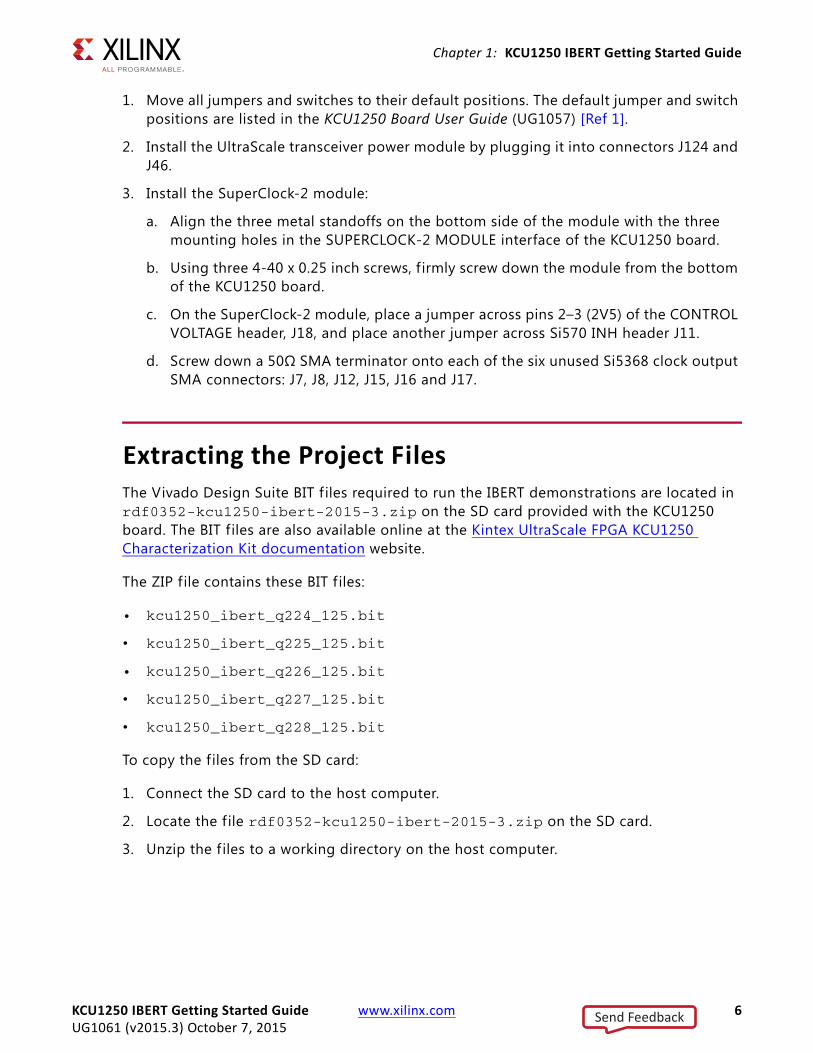
Running the GTH IBERT DemonstrationThe GTH IBERT demonstration operates one GTH Quad at a time. This section describes how to test GTH Quad 224. The remaining GTH Quads can be tested following a similar series of steps.
Connecting the GTH Transceivers and Reference ClocksFigure 1-1 shows the locations for GTH transceiver Quads 224, 225, 226, 227, and 228 on the KCU1250 board.
Figure 1-1 is for reference only and might not reflect the current revision of the board.
Note: QUAD 131 and QUAD 132 are not available on the XCKU040 device.X-Ref Target - Figure 1-1
Figure 1-1: GTH Quad Locations
KCU1250 IBERT Getting Started Guide www.xilinx.com 7UG1061 (v2015.3) October 7, 2015
Send Feedback
Chapter 1: KCU1250 IBERT Getting Started Guide
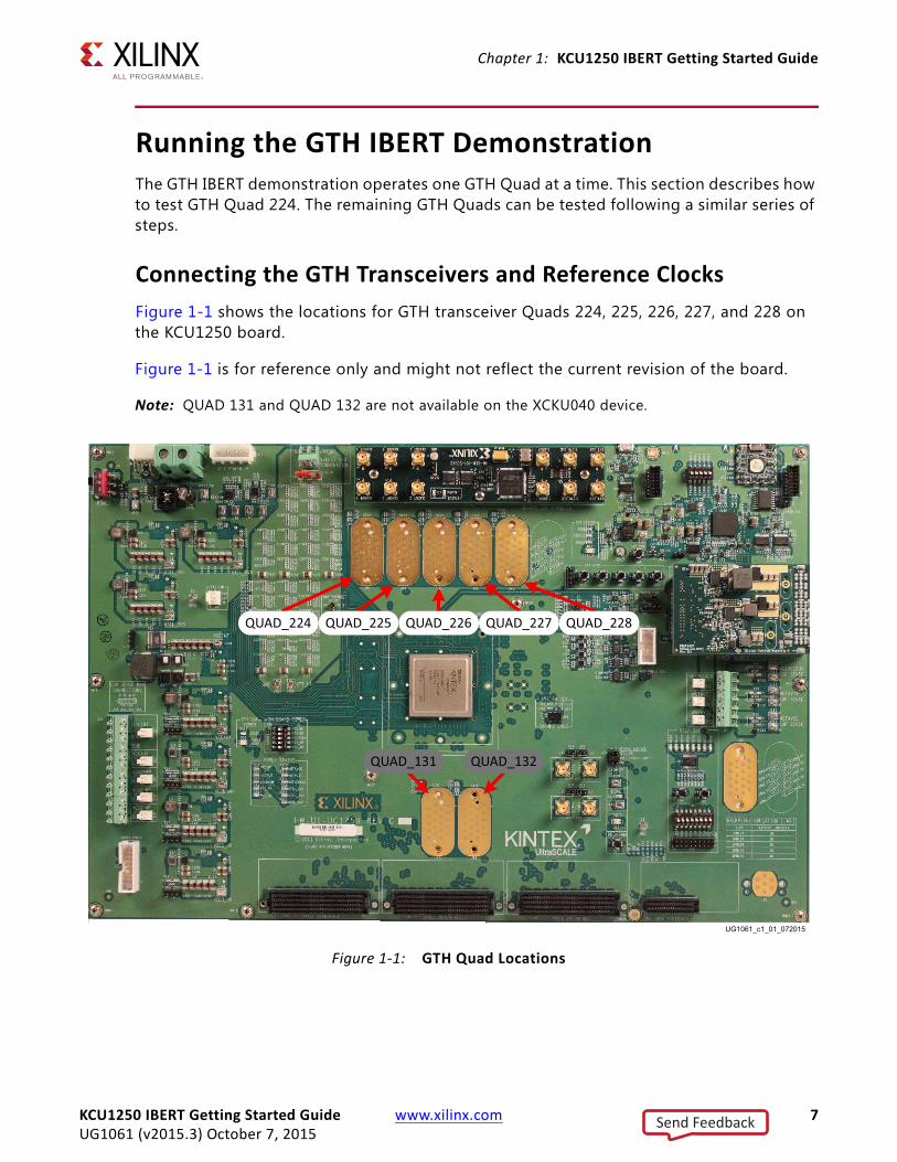
All GTH transceiver pins and reference clock pins are routed from the FPGA to a connector pad that interfaces with Samtec BullsEye connectors. Figure 1-2 A shows the connector pad. Figure 1-2 B shows the connector pinout.
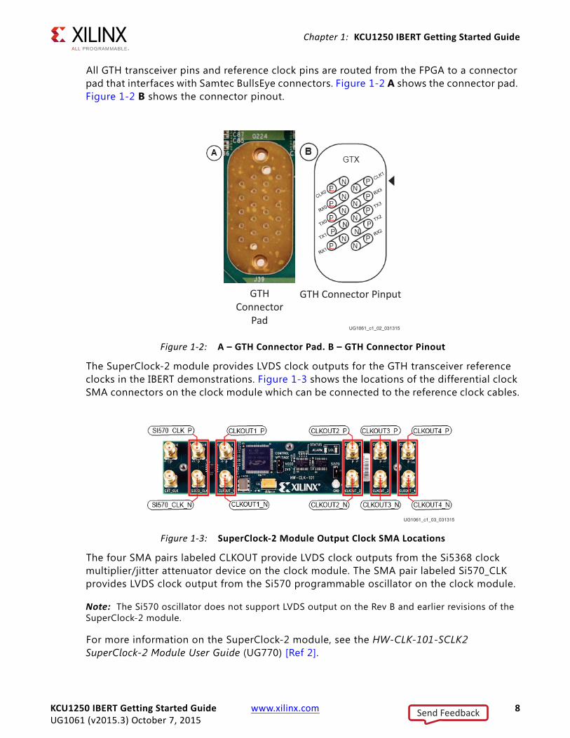
The SuperClock-2 module provides LVDS clock outputs for the GTH transceiver reference clocks in the IBERT demonstrations. Figure 1-3 shows the locations of the differential clock SMA connectors on the clock module which can be connected to the reference clock cables.
The four SMA pairs labeled CLKOUT provide LVDS clock outputs from the Si5368 clock multiplier/jitter attenuator device on the clock module. The SMA pair labeled Si570_CLK provides LVDS clock output from the Si570 programmable oscillator on the clock module.
Note: The Si570 oscillator does not support LVDS output on the Rev B and earlier revisions of the SuperClock-2 module.
For more information on the SuperClock-2 module, see the HW-CLK-101-SCLK2 SuperClock-2 Module User Guide (UG770) [Ref 2].
X-Ref Target - Figure 1-2
Figure 1-2: A – GTH Connector Pad. B – GTH Connector Pinout
X-Ref Target - Figure 1-3
Figure 1-3: SuperClock-2 Module Output Clock SMA Locations
KCU1250 IBERT Getting Started Guide www.xilinx.com 8UG1061 (v2015.3) October 7, 2015
Send Feedback
Chapter 1: KCU1250 IBERT Getting Started Guide
Attach the GTH Quad Connector
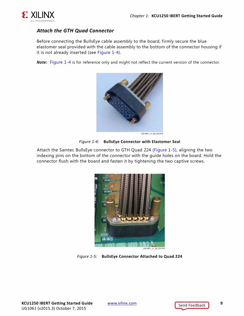
Before connecting the BullsEye cable assembly to the board, f irmly secure the blue elastomer seal provided with the cable assembly to the bottom of the connector housing if it is not already inserted (see Figure 1-4).
Note: Figure 1-4 is for reference only and might not reflect the current version of the connector.
Attach the Samtec BullsEye connector to GTH Quad 224 (Figure 1-5), aligning the two indexing pins on the bottom of the connector with the guide holes on the board. Hold the connector flush with the board and fasten it by tightening the two captive screws.
X-Ref Target - Figure 1-4
Figure 1-4: BullsEye Connector with Elastomer Seal
X-Ref Target - Figure 1-5
Figure 1-5: BullsEye Connector Attached to Quad 224
KCU1250 IBERT Getting Started Guide www.xilinx.com 9UG1061 (v2015.3) October 7, 2015
Send Feedback
Chapter 1: KCU1250 IBERT Getting Started Guide
GTH Transceiver Clock Connections
See Figure 1-2 to identify the P and N coax cables that are connected to the CLK0 reference clock inputs. Connect these cables to the SuperClock-2 module as follows:
• CLK0_P coax cable → SMA connector J7 (CLKOUT1_P) on the SuperClock-2 module
• CLK0_N coax cable → SMA connector J8 (CLKOUT1_N) on the SuperClock-2 module
Note: Any one of the f ive differential outputs from the SuperClock-2 module can be used to source the GTH reference clock. CLKOUT1_P and CLKOUT1_N are used here as an example.
GTH TX/RX Loopback Connections
See Figure 1-2 to identify the P and N coax cables that are connected to the four receivers (RX0, RX1, RX2, and RX3) and the four transmitters (TX0, TX1, TX2, and TX3). Use eight SMA female-to-female (F-F) adapters (Figure 1-6) to connect the transmit and receive cables as shown in Figure 1-7:
• TX0_P → SMA F-F Adapter → RX0_P
• TX0_N → SMA F-F Adapter → RX0_N
• TX1_P → SMA F-F Adapter → RX1_P
• TX1_N → SMA F-F Adapter → RX1_N
• TX2_P → SMA F-F Adapter → RX2_P
• TX2_N → SMA F-F Adapter → RX2_N
• TX3_P → SMA F-F Adapter → RX3_P
• TX3_N → SMA F-F Adapter → RX3_N
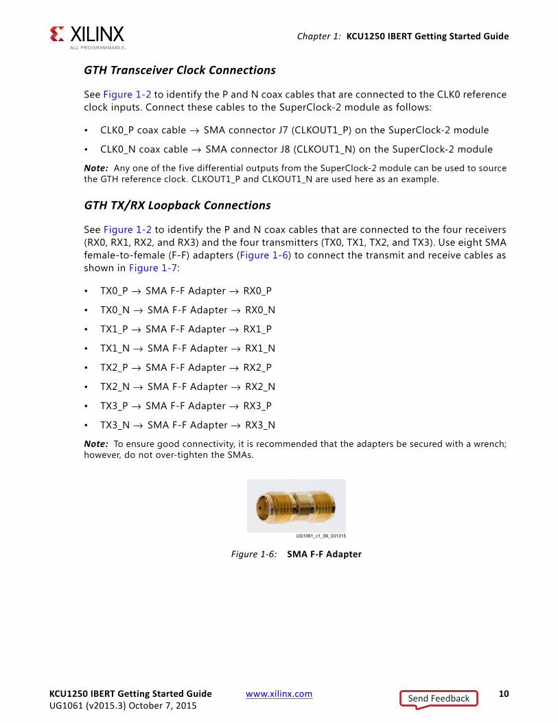
Note: To ensure good connectivity, it is recommended that the adapters be secured with a wrench; however, do not over-tighten the SMAs.X-Ref Target - Figure 1-6
Figure 1-6: SMA F-F Adapter
KCU1250 IBERT Getting Started Guide www.xilinx.com 10UG1061 (v2015.3) October 7, 2015
Send Feedback
Chapter 1: KCU1250 IBERT Getting Started Guide
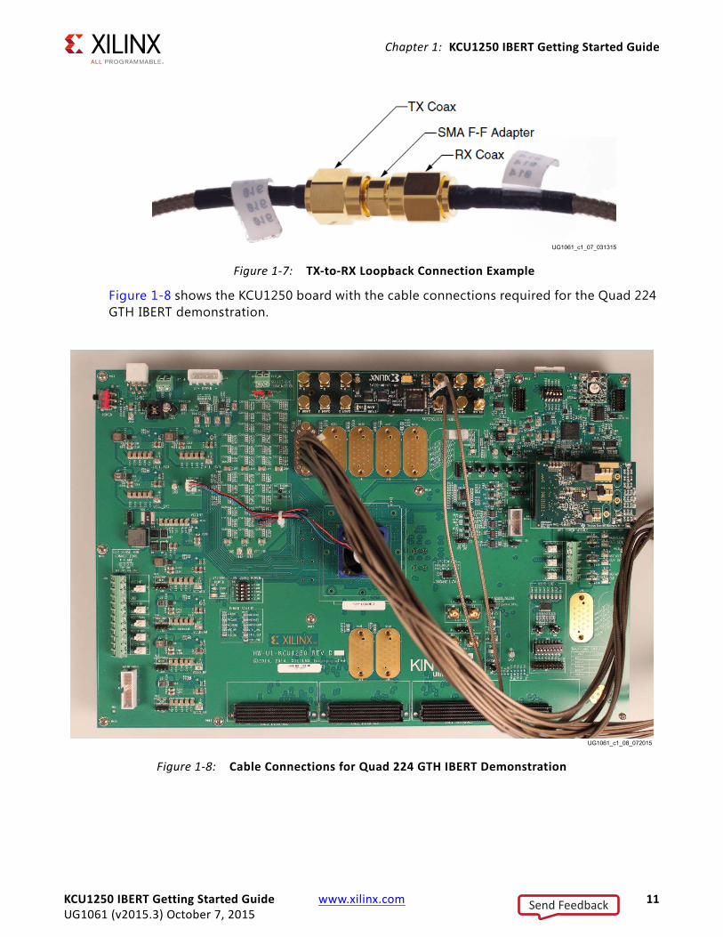
Figure 1-8 shows the KCU1250 board with the cable connections required for the Quad 224 GTH IBERT demonstration.
X-Ref Target - Figure 1-7
Figure 1-7: TX-to-RX Loopback Connection Example
X-Ref Target - Figure 1-8
Figure 1-8: Cable Connections for Quad 224 GTH IBERT Demonstration
KCU1250 IBERT Getting Started Guide www.xilinx.com 11UG1061 (v2015.3) October 7, 2015
Send Feedback
Chapter 1: KCU1250 IBERT Getting Started Guide
Starting the SuperClock-2 ModuleThe SuperClock-2 module features two clock-source components:
• Always-on Si570 crystal oscillator
• Si5368 jitter-attenuating clock multiplier
Outputs from either source can be used to drive the transceiver reference clocks.
To start the SuperClock-2 module:
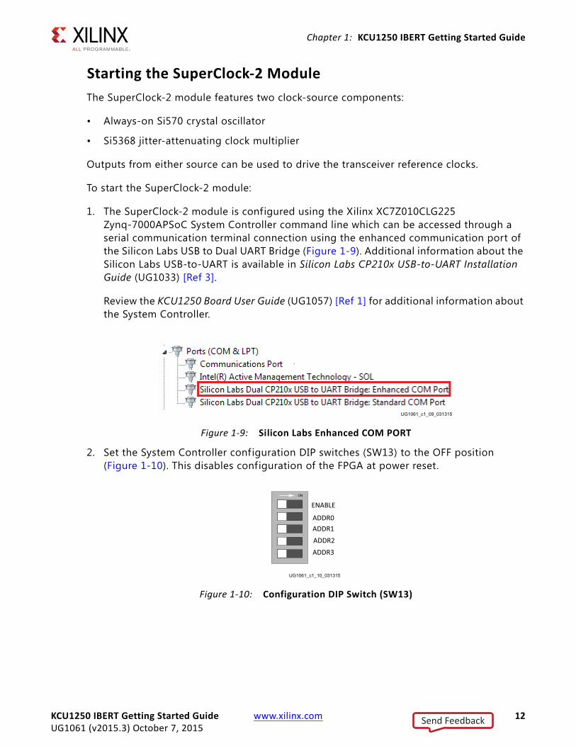
1. The SuperClock-2 module is configured using the Xilinx XC7Z010CLG225 Zynq-7000APSoC System Controller command line which can be accessed through a serial communication terminal connection using the enhanced communication port of the Silicon Labs USB to Dual UART Bridge (Figure 1-9). Additional information about the Silicon Labs USB-to-UART is available in Silicon Labs CP210x USB-to-UART Installation Guide (UG1033) [Ref 3].
Review the KCU1250 Board User Guide (UG1057) [Ref 1] for additional information about the System Controller.
2. Set the System Controller configuration DIP switches (SW13) to the OFF position (Figure 1-10). This disables configuration of the FPGA at power reset.
X-Ref Target - Figure 1-9
Figure 1-9: Silicon Labs Enhanced COM PORT
X-Ref Target - Figure 1-10
Figure 1-10: Configuration DIP Switch (SW13)
KCU1250 IBERT Getting Started Guide www.xilinx.com 12UG1061 (v2015.3) October 7, 2015
Send Feedback
Chapter 1: KCU1250 IBERT Getting Started Guide
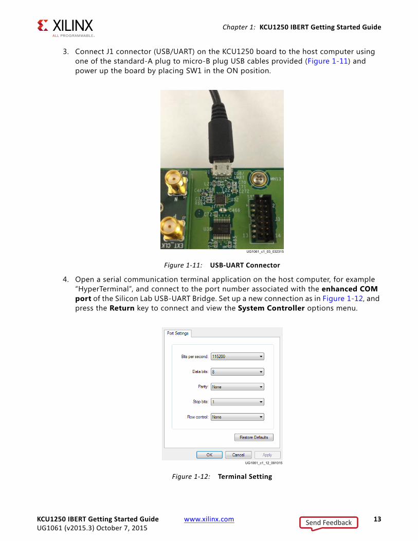
3. Connect J1 connector (USB/UART) on the KCU1250 board to the host computer using one of the standard-A plug to micro-B plug USB cables provided (Figure 1-11) and power up the board by placing SW1 in the ON position.
4. Open a serial communication terminal application on the host computer, for example “HyperTerminal”, and connect to the port number associated with the enhanced COM port of the Silicon Lab USB-UART Bridge. Set up a new connection as in Figure 1-12, and press the Return key to connect and view the System Controller options menu.
X-Ref Target - Figure 1-11
Figure 1-11: USB-UART Connector
X-Ref Target - Figure 1-12
Figure 1-12: Terminal Setting
KCU1250 IBERT Getting Started Guide www.xilinx.com 13UG1061 (v2015.3) October 7, 2015
Send Feedback
Chapter 1: KCU1250 IBERT Getting Started Guide
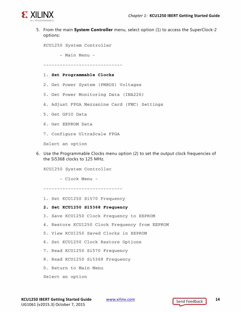
5. From the main System Controller menu, select option (1) to access the SuperClock-2 options:
KCU1250 System Controller
- Main Menu -
-----------------------------
1. Set Programmable Clocks
2. Get Power System (PMBUS) Voltages
3. Get Power Monitoring Data (INA226)
4. Adjust FPGA Mezzanine Card (FMC) Settings
5. Get GPIO Data
6. Get EEPROM Data
7. Configure UltraScale FPGA
Select an option
6. Use the Programmable Clocks menu option (2) to set the output clock frequencies of the Si5368 clocks to 125 MHz.
KCU1250 System Controller
- Clock Menu -
-----------------------------
1. Set KCU1250 Si570 Frequency
2. Set KCU1250 Si5368 Frequency
3. Save KCU1250 Clock Frequency to EEPROM
4. Restore KCU1250 Clock Frequency from EEPROM
5. View KCU1250 Saved Clocks in EEPROM
6. Set KCU1250 Clock Restore Options
7. Read KCU1250 Si570 Frequency
8. Read KCU1250 Si5368 Frequency
0. Return to Main Menu
Select an option
KCU1250 IBERT Getting Started Guide www.xilinx.com 14UG1061 (v2015.3) October 7, 2015
Send Feedback
Chapter 1: KCU1250 IBERT Getting Started Guide
7. Select option 2 (Free-Run crystal) operating mode when prompted.
Choose si5368 operating mode:
1 - Auto-Select
2 - Free-Run using XA-XB crystal
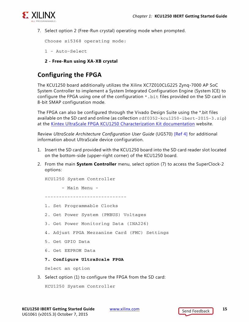
Configuring the FPGAThe KCU1250 board additionally utilizes the Xilinx XC7Z010CLG225 Zynq-7000 AP SoC System Controller to implement a System Integrated Configuration Engine (System ICE) to configure the FPGA using one of the configuration *.bit f iles provided on the SD card in 8-bit SMAP configuration mode.
The FPGA can also be configured through the Vivado Design Suite using the *.bit f iles available on the SD card and online (as collection rdf0352-kcu1250-ibert-2015-3.zip) at the Kintex UltraScale FPGA KCU1250 Characterization Kit documentation website.
Review UltraScale Architecture Configuration User Guide (UG570) [Ref 4] for additional information about UltraScale device configuration.
1. Insert the SD card provided with the KCU1250 board into the SD card reader slot located on the bottom-side (upper-right corner) of the KCU1250 board.
2. From the main System Controller menu, select option (7) to access the SuperClock-2 options:
KCU1250 System Controller
- Main Menu -
-----------------------------
1. Set Programmable Clocks
2. Get Power System (PMBUS) Voltages
3. Get Power Monitoring Data (INA226)
4. Adjust FPGA Mezzanine Card (FMC) Settings
5. Get GPIO Data
6. Get EEPROM Data
7. Configure UltraScale FPGA
Select an option
3. Select option (1) to configure the FPGA from the SD card:
KCU1250 System Controller
KCU1250 IBERT Getting Started Guide www.xilinx.com 15UG1061 (v2015.3) October 7, 2015
Send Feedback
Chapter 1: KCU1250 IBERT Getting Started Guide
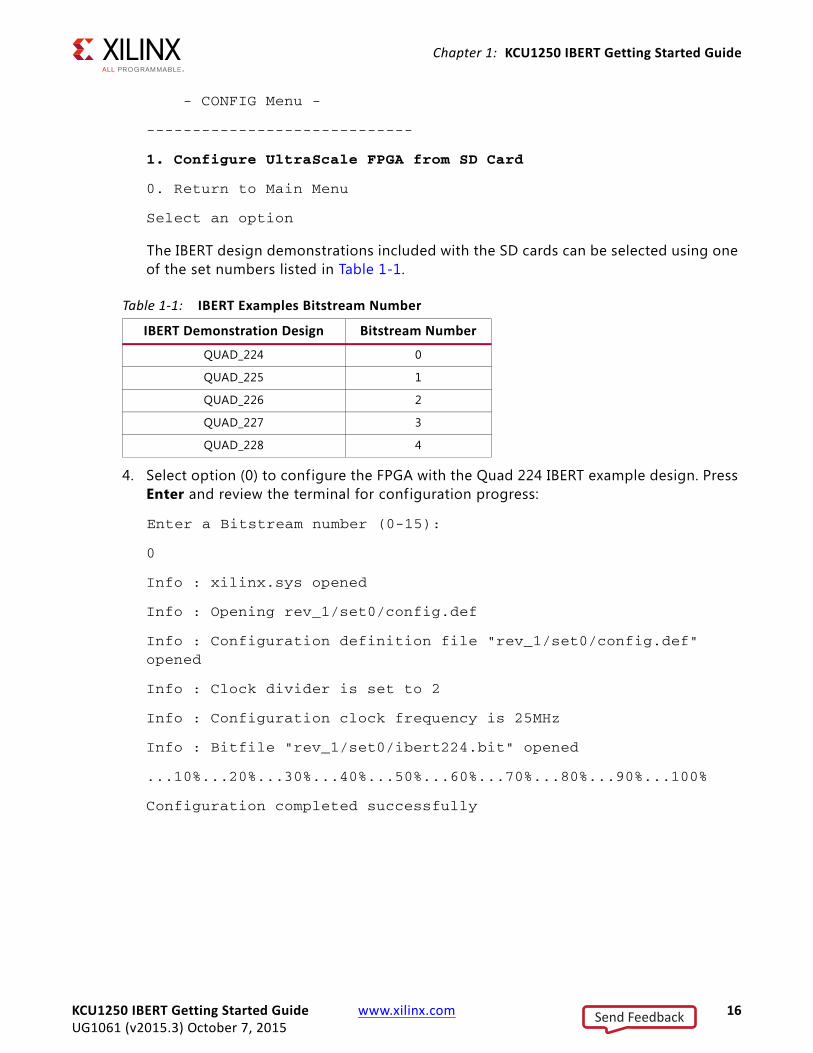
- CONFIG Menu -
-----------------------------
1. Configure UltraScale FPGA from SD Card
0. Return to Main Menu
Select an option
The IBERT design demonstrations included with the SD cards can be selected using one of the set numbers listed in Table 1-1.
4. Select option (0) to configure the FPGA with the Quad 224 IBERT example design. Press Enter and review the terminal for configuration progress:
Enter a Bitstream number (0-15):
0
Info : xilinx.sys opened
Info : Opening rev_1/set0/config.def
Info : Configuration definition file "rev_1/set0/config.def" opened
Info : Clock divider is set to 2
Info : Configuration clock frequency is 25MHz
Info : Bitfile "rev_1/set0/ibert224.bit" opened
...10%...20%...30%...40%...50%...60%...70%...80%...90%...100%
Configuration completed successfully
Table 1-1: IBERT Examples Bitstream Number
IBERT Demonstration Design Bitstream Number
QUAD_224 0
QUAD_225 1
QUAD_226 2
QUAD_227 3
QUAD_228 4
KCU1250 IBERT Getting Started Guide www.xilinx.com 16UG1061 (v2015.3) October 7, 2015
Send Feedback
Chapter 1: KCU1250 IBERT Getting Started Guide
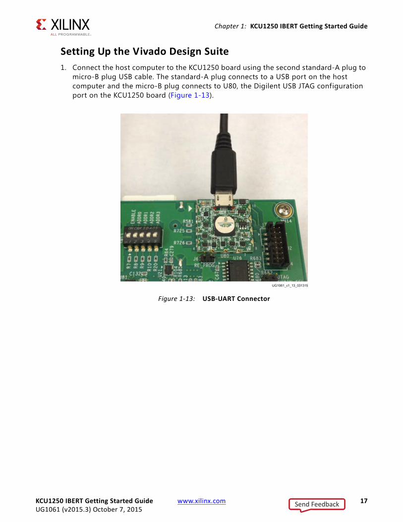
Setting Up the Vivado Design Suite1. Connect the host computer to the KCU1250 board using the second standard-A plug to
micro-B plug USB cable. The standard-A plug connects to a USB port on the host computer and the micro-B plug connects to U80, the Digilent USB JTAG configuration port on the KCU1250 board (Figure 1-13).
X-Ref Target - Figure 1-13
Figure 1-13: USB-UART Connector
KCU1250 IBERT Getting Started Guide www.xilinx.com 17UG1061 (v2015.3) October 7, 2015
Send Feedback
Chapter 1: KCU1250 IBERT Getting Started Guide
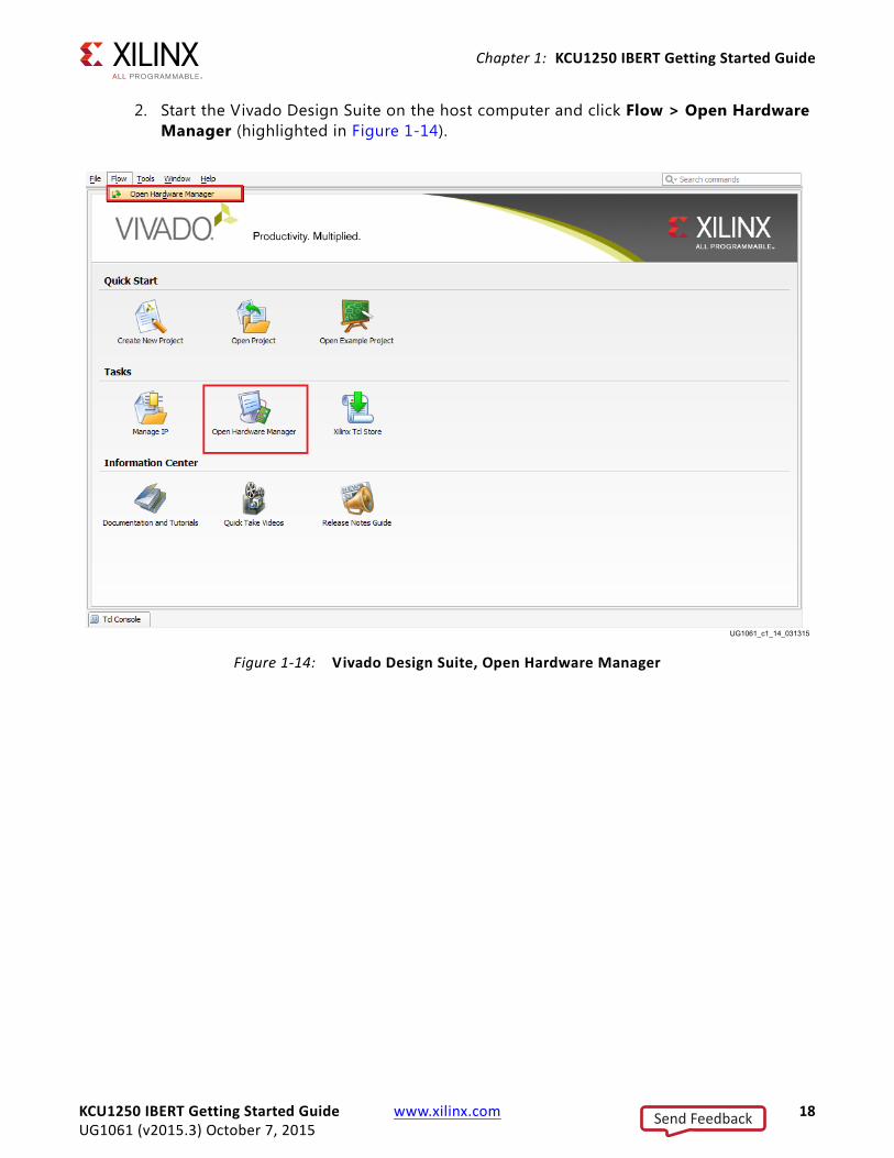
2. Start the Vivado Design Suite on the host computer and click Flow > Open Hardware Manager (highlighted in Figure 1-14).
X-Ref Target - Figure 1-14
Figure 1-14: Vivado Design Suite, Open Hardware Manager
KCU1250 IBERT Getting Started Guide www.xilinx.com 18UG1061 (v2015.3) October 7, 2015
Send Feedback
Chapter 1: KCU1250 IBERT Getting Started Guide
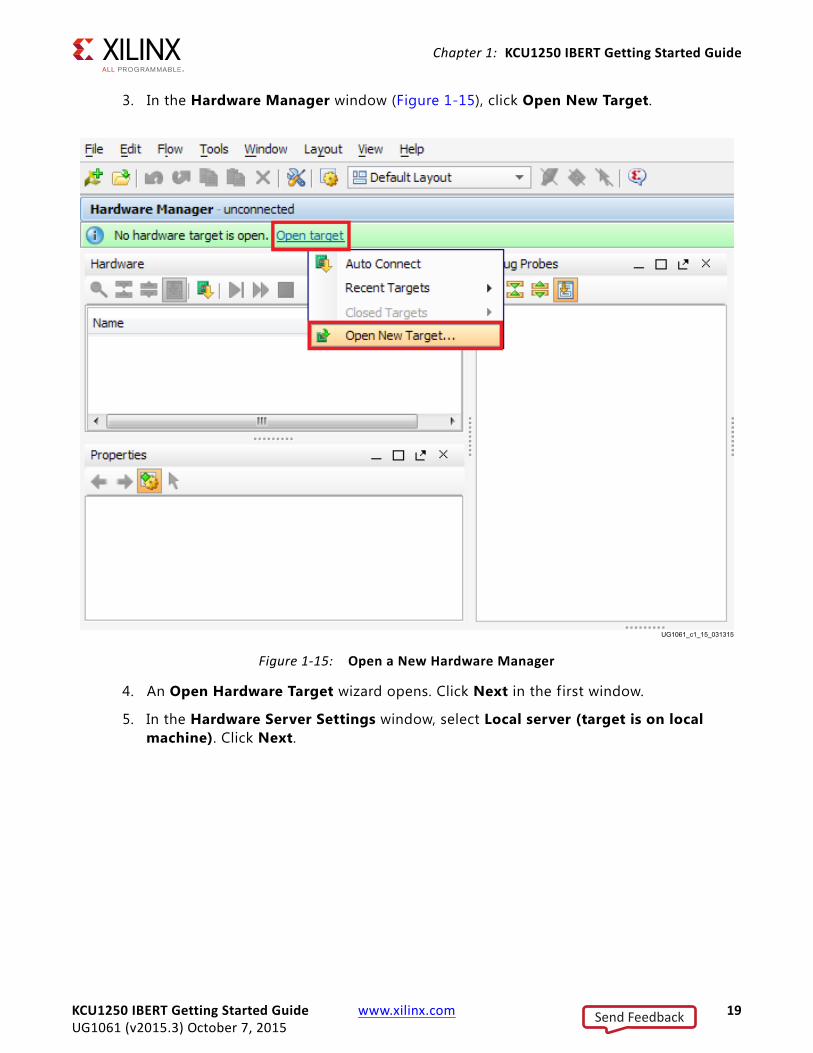
3. In the Hardware Manager window (Figure 1-15), click Open New Target.
4. An Open Hardware Target wizard opens. Click Next in the first window.
5. In the Hardware Server Settings window, select Local server (target is on local machine). Click Next.
X-Ref Target - Figure 1-15
Figure 1-15: Open a New Hardware Manager
KCU1250 IBERT Getting Started Guide www.xilinx.com 19UG1061 (v2015.3) October 7, 2015
Send Feedback
Chapter 1: KCU1250 IBERT Getting Started Guide
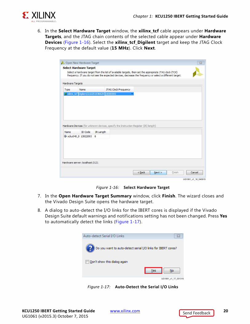
6. In the Select Hardware Target window, the xilinx_tcf cable appears under Hardware Targets, and the JTAG chain contents of the selected cable appear under Hardware Devices (Figure 1-16). Select the xilinx_tcf_Digilent target and keep the JTAG Clock Frequency at the default value (15 MHz). Click Next.
7. In the Open Hardware Target Summary window, click Finish. The wizard closes and the Vivado Design Suite opens the hardware target.
8. A dialog to auto-detect the I/O links for the IBERT cores is displayed if the Vivado Design Suite default warnings and notif ications setting has not been changed. Press Yes to automatically detect the links (Figure 1-17).
X-Ref Target - Figure 1-16
Figure 1-16: Select Hardware Target
X-Ref Target - Figure 1-17
Figure 1-17: Auto-Detect the Serial I/O Links
KCU1250 IBERT Getting Started Guide www.xilinx.com 20UG1061 (v2015.3) October 7, 2015
Send Feedback
Chapter 1: KCU1250 IBERT Getting Started Guide
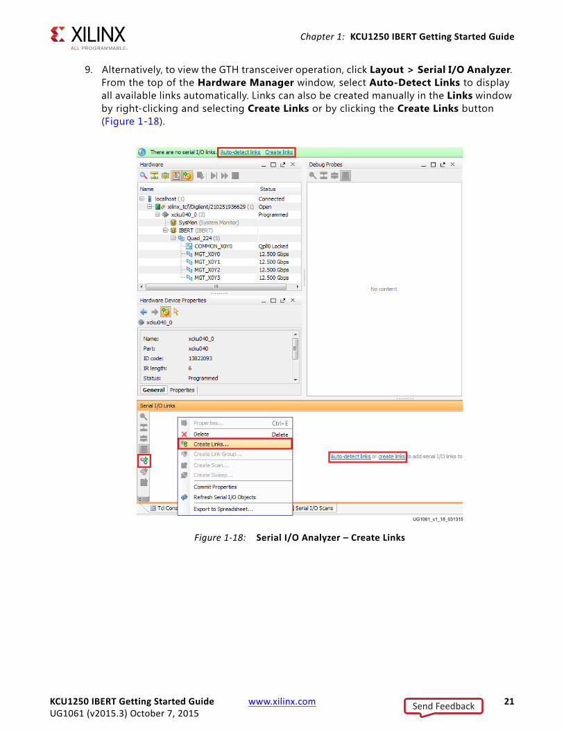
9. Alternatively, to view the GTH transceiver operation, click Layout > Serial I/O Analyzer. From the top of the Hardware Manager window, select Auto-Detect Links to display all available links automatically. Links can also be created manually in the Links window by right-clicking and selecting Create Links or by clicking the Create Links button (Figure 1-18).
X-Ref Target - Figure 1-18
Figure 1-18: Serial I/O Analyzer – Create Links
KCU1250 IBERT Getting Started Guide www.xilinx.com 21UG1061 (v2015.3) October 7, 2015
Send Feedback
Chapter 1: KCU1250 IBERT Getting Started Guide
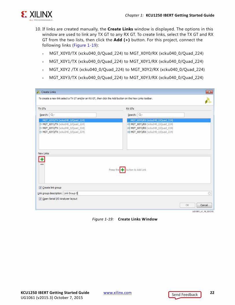
10. If links are created manually, the Create Links window is displayed. The options in this window are used to link any TX GT to any RX GT. To create links, select the TX GT and RX GT from the two lists, then click the Add (+) button. For this project, connect the following links (Figure 1-19):
° MGT_X0Y0/TX (xcku040_0/Quad_224) to MGT_X0Y0/RX (xcku040_0/Quad_224)
° MGT_X0Y1/TX (xcku040_0/Quad_224) to MGT_X0Y1/RX (xcku040_0/Quad_224)
° MGT_X0Y2 /TX (xcku040_0/Quad_224) to MGT_X0Y2/RX (xcku040_0/Quad_224)
° MGT_X0Y3/TX (xcku040_0/Quad_224) to MGT_X0Y3/RX (xcku040_0/Quad_224)X-Ref Target - Figure 1-19
Figure 1-19: Create Links Window
KCU1250 IBERT Getting Started Guide www.xilinx.com 22UG1061 (v2015.3) October 7, 2015
Send Feedback
Chapter 1: KCU1250 IBERT Getting Started Guide
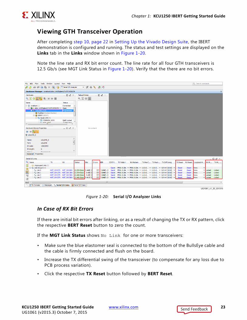
Viewing GTH Transceiver OperationAfter completing step 10, page 22 in Setting Up the Vivado Design Suite, the IBERT demonstration is configured and running. The status and test settings are displayed on the Links tab in the Links window shown in Figure 1-20.
Note the line rate and RX bit error count. The line rate for all four GTH transceivers is 12.5 Gb/s (see MGT Link Status in Figure 1-20). Verify that the there are no bit errors.
In Case of RX Bit Errors
If there are initial bit errors after linking, or as a result of changing the TX or RX pattern, click the respective BERT Reset button to zero the count.
If the MGT Link Status shows No Link for one or more transceivers:
• Make sure the blue elastomer seal is connected to the bottom of the BullsEye cable and the cable is f irmly connected and flush on the board.
• Increase the TX differential swing of the transceiver (to compensate for any loss due to PCB process variation).
• Click the respective TX Reset button followed by BERT Reset.
X-Ref Target - Figure 1-20
Figure 1-20: Serial I/O Analyzer Links
KCU1250 IBERT Getting Started Guide www.xilinx.com 23UG1061 (v2015.3) October 7, 2015
Send Feedback

Chapter 1: KCU1250 IBERT Getting Started Guide
Additional information on the Vivado Design Suite and IBERT core can be found in Vivado Design Suite User Guide: Programming and Debugging (UG908) [Ref 5].
Closing the IBERT DemonstrationTo stop the IBERT demonstration:
1. Close the Vivado Design Suite by selecting File > Exit.
2. Place the main power switch SW1 in the OFF position.
KCU1250 IBERT Getting Started Guide www.xilinx.com 24UG1061 (v2015.3) October 7, 2015
Send Feedback
Chapter 2
Creating the GTH IBERT CoreNote: Vivado® Design Suite 2015.3 is required to rebuild the designs shown here.
This section provides a procedure to create a single Quad GTH IBERT core. The procedure assumes Quad 224 at 12.5 Gb/s line rate, but cores for any of the GTH Quads with any supported line rate can be created following the same series of steps.
For more details on generating IBERT cores, see the Vivado Design Suite User Guide: Programming and Debugging (UG908) [Ref 5].
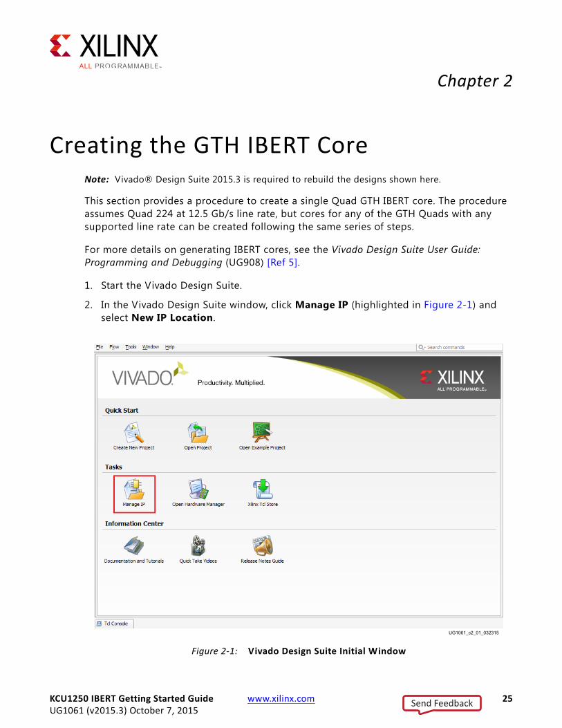
1. Start the Vivado Design Suite.
2. In the Vivado Design Suite window, click Manage IP (highlighted in Figure 2-1) and select New IP Location.
X-Ref Target - Figure 2-1
Figure 2-1: Vivado Design Suite Initial Window
KCU1250 IBERT Getting Started Guide www.xilinx.com 25UG1061 (v2015.3) October 7, 2015
Send Feedback
Chapter 2: Creating the GTH IBERT Core
3. A Create a New Customized IP Location dialog window opens (not shown), Click Next.
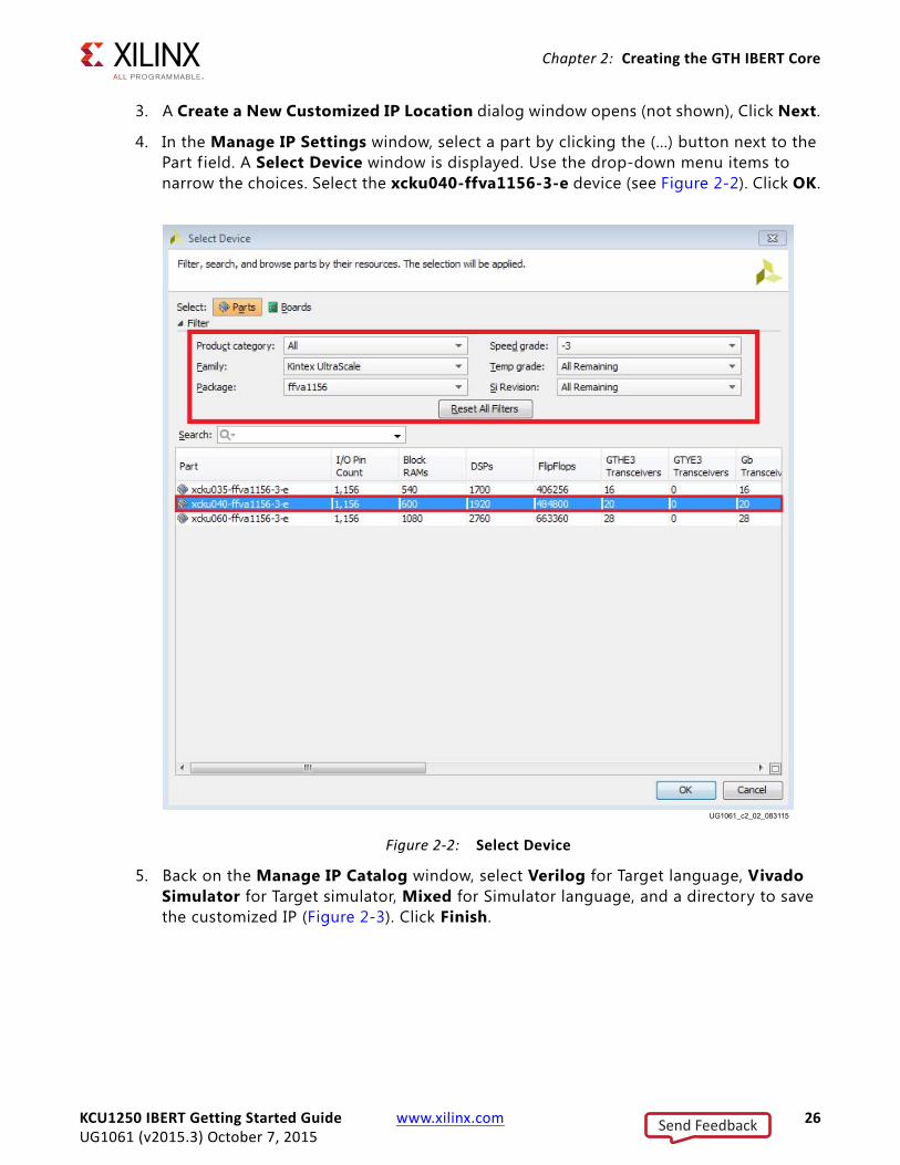
4. In the Manage IP Settings window, select a part by clicking the (...) button next to the Part f ield. A Select Device window is displayed. Use the drop-down menu items to narrow the choices. Select the xcku040-ffva1156-3-e device (see Figure 2-2). Click OK.
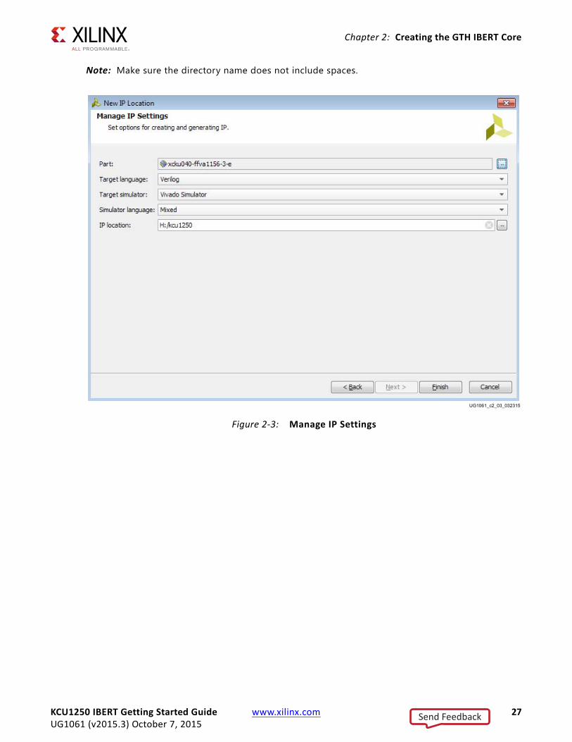
5. Back on the Manage IP Catalog window, select Verilog for Target language, Vivado Simulator for Target simulator, Mixed for Simulator language, and a directory to save the customized IP (Figure 2-3). Click Finish.
X-Ref Target - Figure 2-2
Figure 2-2: Select Device
KCU1250 IBERT Getting Started Guide www.xilinx.com 26UG1061 (v2015.3) October 7, 2015
Send Feedback
Chapter 2: Creating the GTH IBERT Core
Note: Make sure the directory name does not include spaces.X-Ref Target - Figure 2-3
Figure 2-3: Manage IP Settings
KCU1250 IBERT Getting Started Guide www.xilinx.com 27UG1061 (v2015.3) October 7, 2015
Send Feedback
Chapter 2: Creating the GTH IBERT Core
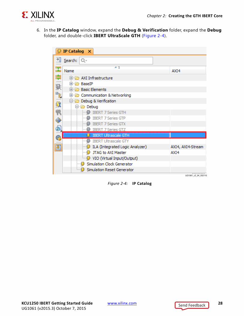
6. In the IP Catalog window, expand the Debug & Verification folder, expand the Debug folder, and double-click IBERT UltraScale GTH (Figure 2-4).
X-Ref Target - Figure 2-4
Figure 2-4: IP Catalog
KCU1250 IBERT Getting Started Guide www.xilinx.com 28UG1061 (v2015.3) October 7, 2015
Send Feedback
Chapter 2: Creating the GTH IBERT Core
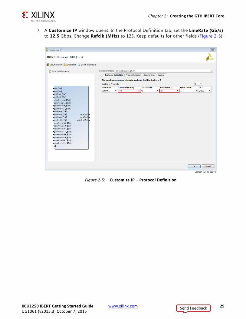
7. A Customize IP window opens. In the Protocol Definition tab, set the LineRate (Gb/s) to 12.5 Gbps. Change Refclk (MHz) to 125. Keep defaults for other f ields (Figure 2-5).
X-Ref Target - Figure 2-5
Figure 2-5: Customize IP – Protocol Definition
KCU1250 IBERT Getting Started Guide www.xilinx.com 29UG1061 (v2015.3) October 7, 2015
Send Feedback
Chapter 2: Creating the GTH IBERT Core
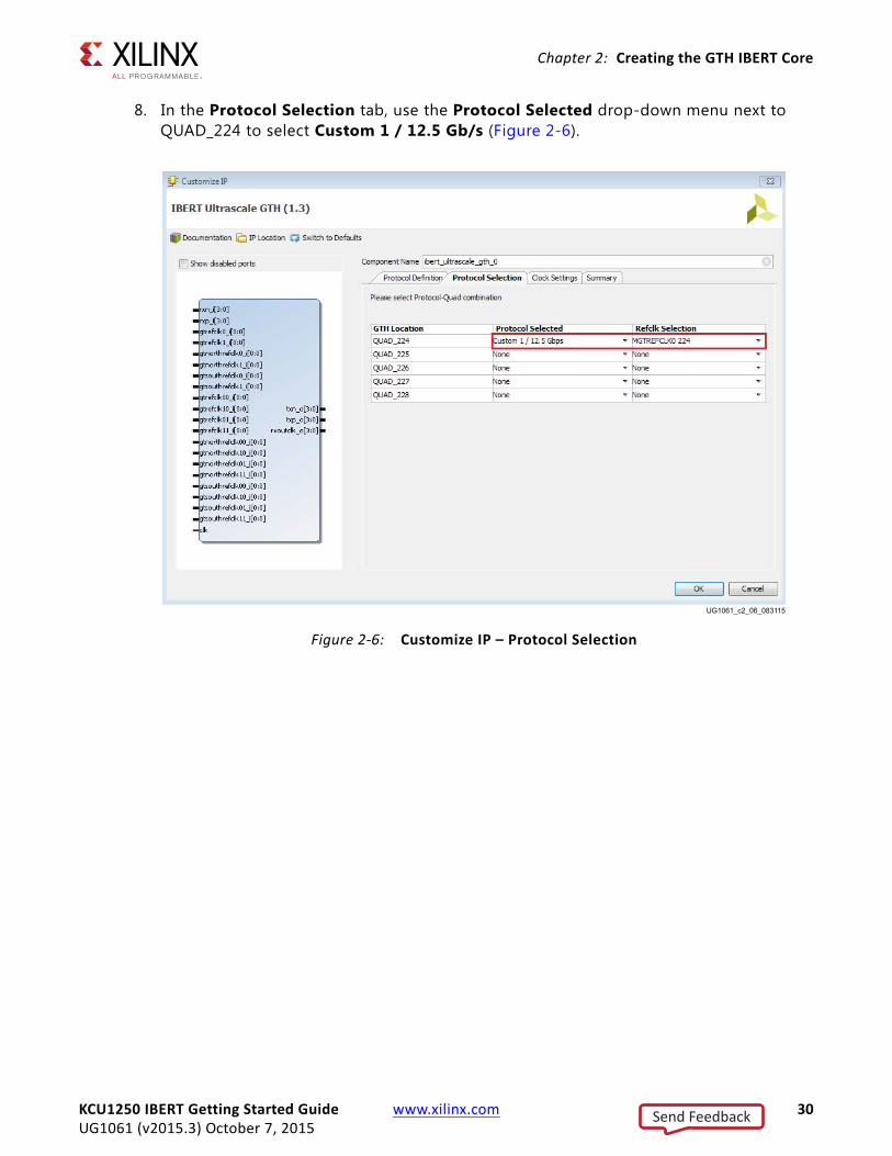
8. In the Protocol Selection tab, use the Protocol Selected drop-down menu next to QUAD_224 to select Custom 1 / 12.5 Gb/s (Figure 2-6).
X-Ref Target - Figure 2-6
Figure 2-6: Customize IP – Protocol Selection
KCU1250 IBERT Getting Started Guide www.xilinx.com 30UG1061 (v2015.3) October 7, 2015
Send Feedback
Chapter 2: Creating the GTH IBERT Core
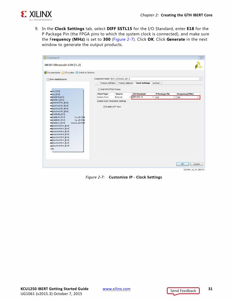
9. In the Clock Settings tab, select DIFF SSTL15 for the I/O Standard, enter E18 for the P Package Pin (the FPGA pins to which the system clock is connected), and make sure the Frequency (MHz) is set to 300 (Figure 2-7). Click OK. Click Generate in the next window to generate the output products.
X-Ref Target - Figure 2-7
Figure 2-7: Customize IP - Clock Settings
KCU1250 IBERT Getting Started Guide www.xilinx.com 31UG1061 (v2015.3) October 7, 2015
Send Feedback
Chapter 2: Creating the GTH IBERT Core
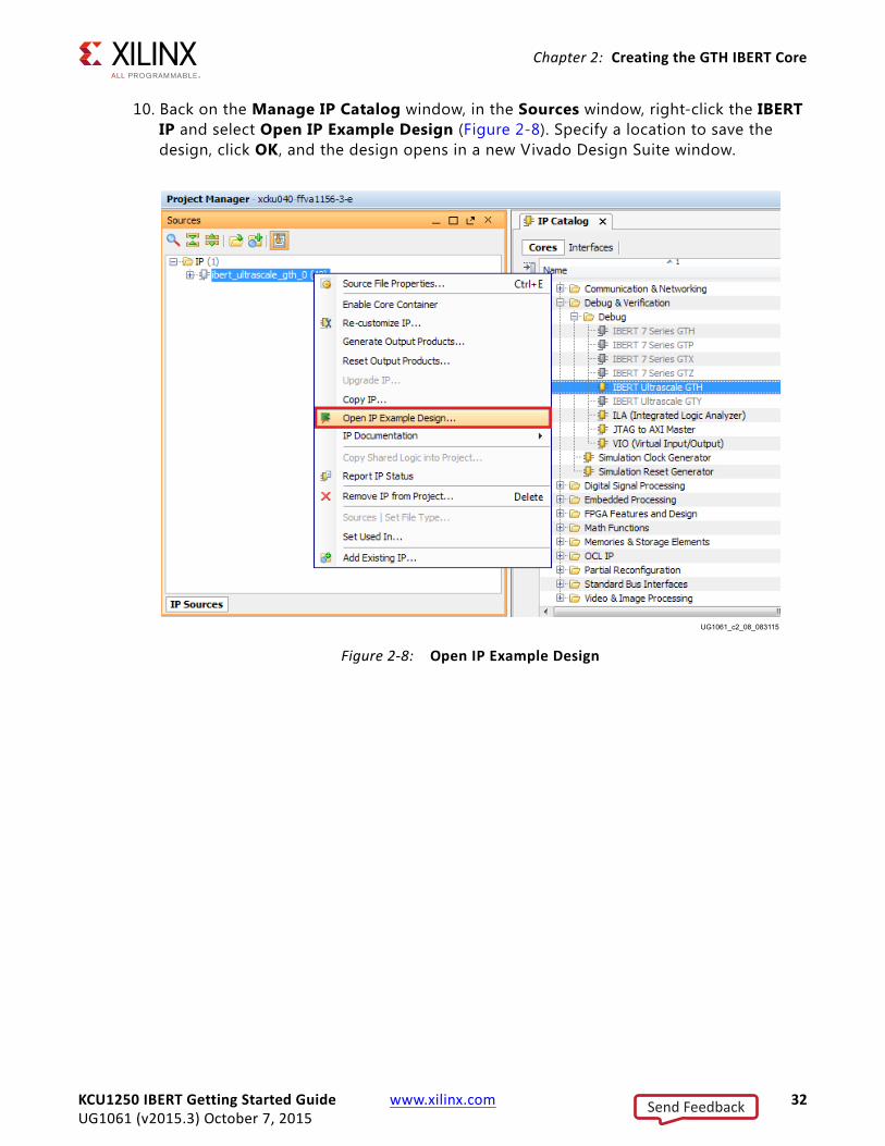
10. Back on the Manage IP Catalog window, in the Sources window, right-click the IBERT IP and select Open IP Example Design (Figure 2-8). Specify a location to save the design, click OK, and the design opens in a new Vivado Design Suite window.
X-Ref Target - Figure 2-8
Figure 2-8: Open IP Example Design
KCU1250 IBERT Getting Started Guide www.xilinx.com 32UG1061 (v2015.3) October 7, 2015
Send Feedback
Chapter 2: Creating the GTH IBERT Core
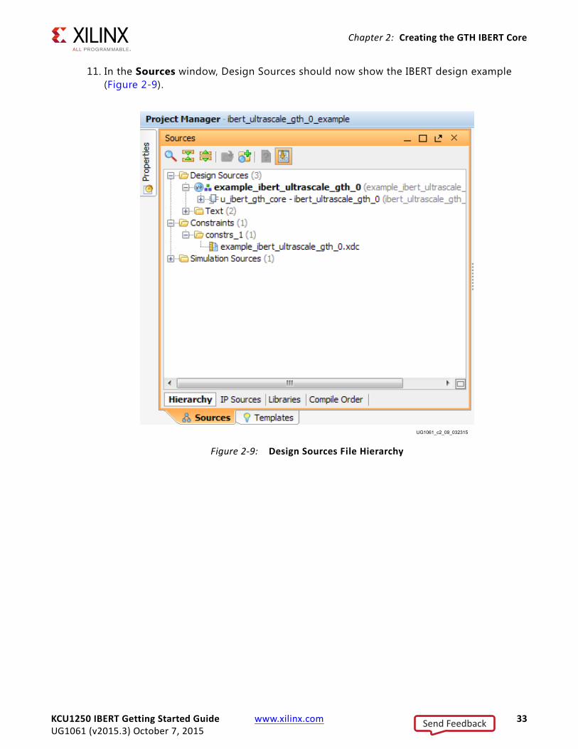
11. In the Sources window, Design Sources should now show the IBERT design example (Figure 2-9).
X-Ref Target - Figure 2-9
Figure 2-9: Design Sources File Hierarchy
KCU1250 IBERT Getting Started Guide www.xilinx.com 33UG1061 (v2015.3) October 7, 2015
Send Feedback
Chapter 2: Creating the GTH IBERT Core
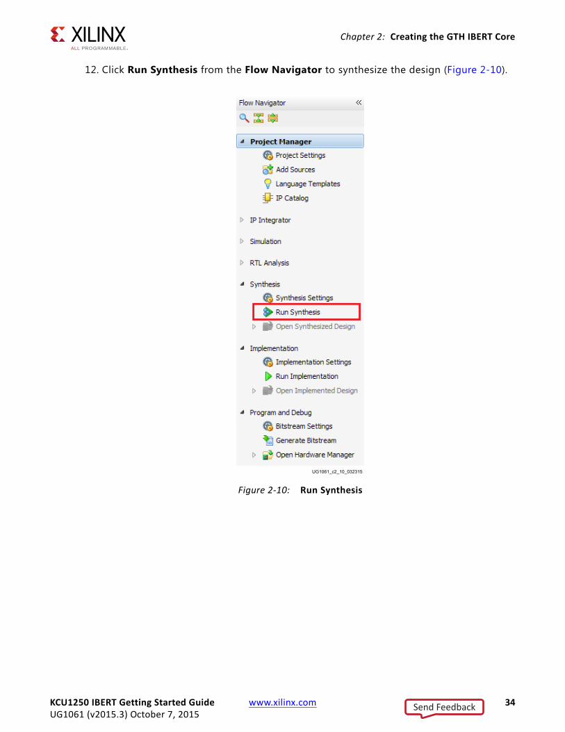
12. Click Run Synthesis from the Flow Navigator to synthesize the design (Figure 2-10).X-Ref Target - Figure 2-10
Figure 2-10: Run Synthesis
KCU1250 IBERT Getting Started Guide www.xilinx.com 34UG1061 (v2015.3) October 7, 2015
Send Feedback
Chapter 2: Creating the GTH IBERT Core
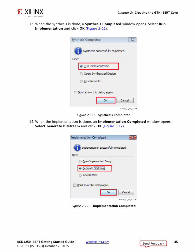
13. When the synthesis is done, a Synthesis Completed window opens. Select Run Implementation and click OK (Figure 2-11).
14. When the implementation is done, an Implementation Completed window opens. Select Generate Bitstream and click OK (Figure 2-12).
X-Ref Target - Figure 2-11
Figure 2-11: Synthesis Completed
X-Ref Target - Figure 2-12
Figure 2-12: Implementation Completed
KCU1250 IBERT Getting Started Guide www.xilinx.com 35UG1061 (v2015.3) October 7, 2015
Send Feedback
Chapter 2: Creating the GTH IBERT Core
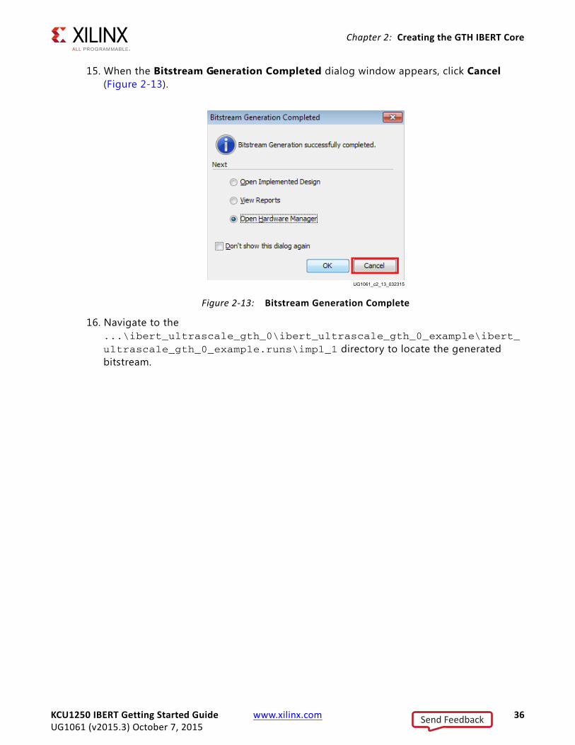
15. When the Bitstream Generation Completed dialog window appears, click Cancel (Figure 2-13).
16. Navigate to the ...\ibert_ultrascale_gth_0\ibert_ultrascale_gth_0_example\ibert_ultrascale_gth_0_example.runs\impl_1 directory to locate the generated bitstream.
X-Ref Target - Figure 2-13
Figure 2-13: Bitstream Generation Complete
KCU1250 IBERT Getting Started Guide www.xilinx.com 36UG1061 (v2015.3) October 7, 2015
Send Feedback
Appendix A
Additional Resources and Legal Notices
Xilinx ResourcesFor support resources such as Answers, Documentation, Downloads, and Forums, see Xilinx Support.
Solution CentersSee the Xilinx Solution Centers for support on devices, software tools, and intellectual property at all stages of the design cycle. Topics include design assistance, advisories, and troubleshooting tips.
ReferencesThe most up to date information related to the KCU1250 kit and its documentation is available on these websites.
Kintex UltraScale FPGA KCU1250 Characterization Kit
Kintex UltraScale FPGA KCU1250 Characterization Kit documentation
Kintex UltraScale FPGA KCU1250 Characterization Kit Master Answer Record (AR 63058)
These Xilinx documents provide supplemental material useful with this guide:
1. KCU1250 Board User Guide (UG1057)
2. HW-CLK-101-SCLK2 SuperClock-2 Module User Guide (UG770)
3. Silicon Labs CP210x USB-to-UART Installation Guide (UG1033)
4. UltraScale Architecture Configuration User Guide (UG570)
5. Vivado Design Suite User Guide: Programming and Debugging (UG908)
6. Kintex UltraScale FPGAs Data Sheet: DC and AC Switching Characteristics (DS892)
KCU1250 IBERT Getting Started Guide www.xilinx.com 37UG1061 (v2015.3) October 7, 2015
Send Feedback
Appendix A: Additional Resources and Legal Notices
7. Zynq-7000 All Programmable SoC Overview (DS190)
8. UltraScale Architecture GTH Transceivers User Guide (UG576)
9. Vivado Design Suite User Guide: Getting Started (UG910)
10. Tera Term Terminal Emulator Installation Guide (UG1036)
11. UltraScale FPGAs Transceivers Wizard LogiCORE IP Product Guide (PG182)
Please Read: Important Legal NoticesThe information disclosed to you hereunder (the “Materials”) is provided solely for the selection and use of Xilinx products. To the maximum extent permitted by applicable law: (1) Materials are made available "AS IS" and with all faults, Xilinx hereby DISCLAIMS ALL WARRANTIES AND CONDITIONS, EXPRESS, IMPLIED, OR STATUTORY, INCLUDING BUT NOT LIMITED TO WARRANTIES OF MERCHANTABILITY, NON-INFRINGEMENT, OR FITNESS FOR ANY PARTICULAR PURPOSE; and (2) Xilinx shall not be liable (whether in contract or tort, including negligence, or under any other theory of liability) for any loss or damage of any kind or nature related to, arising under, or in connection with, the Materials (including your use of the Materials), including for any direct, indirect, special, incidental, or consequential loss or damage (including loss of data, profits, goodwill, or any type of loss or damage suffered as a result of any action brought by a third party) even if such damage or loss was reasonably foreseeable or Xilinx had been advised of the possibility of the same. Xilinx assumes no obligation to correct any errors contained in the Materials or to notify you of updates to the Materials or to product specifications. You may not reproduce, modify, distribute, or publicly display the Materials without prior written consent. Certain products are subject to the terms and conditions of Xilinx’s limited warranty, please refer to Xilinx’s Terms of Sale which can be viewed at http://www.xilinx.com/legal.htm#tos; IP cores may be subject to warranty and support terms contained in a license issued to you by Xilinx. Xilinx products are not designed or intended to be fail-safe or for use in any application requiring fail-safe performance; you assume sole risk and liability for use of Xilinx products in such critical applications, please refer to Xilinx’s Terms of Sale which can be viewed at http://www.xilinx.com/legal.htm#tos.© Copyright 2015 Xilinx, Inc. Xilinx, the Xilinx logo, Artix, ISE, Kintex, Spartan, Virtex, Vivado, Zynq, and other designated brands included herein are trademarks of Xilinx in the United States and other countries. All other trademarks are the property of their respective owners.
KCU1250 IBERT Getting Started Guide www.xilinx.com 38UG1061 (v2015.3) October 7, 2015
Send Feedback

KCU1250 IBERT Getting Started Guide www.xilinx.com 39UG1061 (v2015.3) October 7, 2015
Appendix B
WarrantyTHIS LIMITED WARRANTY applies solely to standard hardware development boards and standard hardware programming cables manufactured by or on behalf of Xilinx (“Development Systems”). Subject to the limitations herein, Xilinx warrants that Development Systems, when delivered by Xilinx or its authorized distributor, for ninety (90) days following the delivery date, will be free from defects in material and workmanship and will substantially conform to Xilinx publicly available specif ications for such products in effect at the time of delivery. This limited warranty excludes: (i) engineering samples or beta versions of Development Systems (which are provided “AS IS” without warranty); (ii) design defects or errors known as “errata”; (iii) Development Systems procured through unauthorized third parties; and (iv) Development Systems that have been subject to misuse, mishandling, accident, alteration, neglect, unauthorized repair or installation. Furthermore, this limited warranty shall not apply to the use of covered products in an application or environment that is not within Xilinx specifications or in the event of any act, error, neglect or default of Customer. For any breach by Xilinx of this limited warranty, the exclusive remedy of Customer and the sole liability of Xilinx shall be, at the option of Xilinx, to replace or repair the affected products, or to refund to Customer the price of the affected products. The availability of replacement products is subject to product discontinuation policies at Xilinx. Customer may not return product without f irst obtaining a customer return material authorization (RMA) number from Xilinx.
THE WARRANTIES SET FORTH HEREIN ARE EXCLUSIVE. XILINX DISCLAIMS ALL OTHER WARRANTIES, WHETHER EXPRESS, IMPLIED OR STATUTORY, INCLUDING, WITHOUT LIMITATION, ANY WARRANTY OF MERCHANTABILITY, FITNESS FOR A PARTICULAR PURPOSE, OR NON-INFRINGEMENT, AND ANY WARRANTY THAT MAY ARISE FROM COURSE OF DEALING, COURSE OF PERFORMANCE, OR USAGE OF TRADE. (2008.10)
Do not throw Xilinx products marked with the “crossed out wheeled bin” in the trash. Directive 2002/96/EC on waste electrical and electronic equipment (WEEE) requires the separate collection of WEEE. Your cooperation is essential in ensuring the proper management of WEEE and the protection of the environment and human health from potential effects arising from the presence of hazardous substances in WEEE. Return the marked products to Xilinx for proper disposal. Further information and instructions for free-of-charge return available at: www.xilinx.com\ehs\weee.htm.
Send Feedback