
Berkenalan dengan Universitas Tohoku Introduction to Tohoku University

KINKENResearch Highlights
Institute for Materials Research, Tohoku University
2017
KINKEN Research Highlights 2017Contents
Preface 4
Research Highlights
1. Infrastructural Materials
Microstructure Design of Structural Metallic Materials Division 8
Nuclear Materials Science Division 9
Multi-Functional Materials Science Division 10
Deformation Processing Division 11
Materials Science of Non-Stoichiometric Compounds Division 12
Analytical Science Division 13
2. Energy-related Materials
Crystal Physics Division 16
Physics of Crystal Defects Division 17
Materials Design by Computer Simulation Division 18
Nuclear Materials Engineering Division 19
Non-Equilibrium Materials Division 20
Hydrogen Functional Materials Division 21
Creation of Life Innovation Materials for Interdisciplinary and International Researcher Development 22
Professional development Consortium for Computational Materials Scientists (PCoMS) 23
3. Electronic Materials
Theory of Solid State Physics Division 26
Magnetism Division 27
Surface and Interface Research Division 28
Low Temperature Physics Division 29
Low Temperature Condensed State Physics Division 30
Metal Physics with Quantum Beam Spectroscopy Division 31
Irradiation Effects in Nuclear and Their Related Materials Division 32
Physics of Electronic Materials Division 33
Chemical Physics of Non-Crystalline Materials Division 34
Solid-State Metal-Complex Chemistry Division 35
Magnetic Materials Division 36
Crystal Chemistry Division 37
Advanced Crystal Engineering Laboratory 38
Actinide Materials Science Division 39
Research Centers
International Research Center for Nuclear Materials Science 42
Cooperative Research and Development Center for Advanced Materials 44
High Field Laboratory for Superconducting Materials 45
Trans-Regional Corporation Center for Industrial Materials Research 46
Center for Computational Materials Science 47
Collaborative Research Center on Energy Materials 48
International Collaboration Center (ICC-IMR) 49
Center of Neutron Science for Advanced Materials 50
Research and Development Center for Ultra High Efficiency Nano-Crystalline Soft Magnetic Materials 51
Laboratory of Low Temperature Materials Science 52
Laboratory of Alpha-Ray Emitters 53
Analytical Research Core for Advanced Materials (ARCAM) 54
Author Index 55
Keyword Index 56
4 IMR KINKEN Research Highlights 2017
Preface
Dear Colleagues,
We are pleased to present KINKEN Research Highlights 2017, which is the annual report that
includes a collection of research outputs of the past year from the Institute for Materials Research (IMR),
Tohoku University KINKEN is the abbreviation for “Kinzoku Zairyo Kenkyujo,” the Japanese name for
IMR, which is well known in the materials science community
IMR celebrated its centenary in 2016 Professor Kotaro Honda established the IMR at the Tohoku
Imperial University in 1916 as the 2nd Division of the Provisional Institute of Physical and Chemical
Research At that time the primary research focus was steel Thereafter, the research domains gradually
broadened to include various types of alloys and metals The name was changed into the Research
Institute for Iron, Steel and Other Metals (RIISOM) in 1922 Subsequently, the institute developed into a
global center for fundamental and applied research covering all types of materials, including nonmetals
In 1987 the institute was reorganized into a national collaborative research institute affiliated with Tohoku
University, and consequently renamed to the present Institute for Materials Research (IMR)
IMR has greatly contributed to the advancement of materials science and engineering The invention
of KS steel in 1916, the strongest permanent magnet at that time, was the first great achievement In
subsequent years, many different types of practically useable materials have successfully been
developed, including new KS steel, Sendust alloy, SiC fibers, various intermetallic compounds, and
more recently, amorphous alloys In addition, considerable effort was dedicated to basic research for
materials development, which paved the way for pioneering research in magnetism, superconductivity,
5IMR KINKEN Research Highlights 2017
Director Prof Koki Takanashi
optical properties, and microstructure analyses of materials Recently, IMR has created a wide array of
new materials, including high-performance, high-quality, and multifunctional materials such as bulk
metallic glasses, nanostructured materials, nanocomposites, ceramics, crystals, oxides, nitrides,
hydrides, complexes, organic materials, etc, which are useful for electronic, optical, magnetic, spintronic,
biological, energetic, and infrastructural applications
In the 21st Century, we face worldwide environmental problems such as global warming and the
depletion of resources and energy There is an increasing need to preserve the environment and work
towards achieving sustainable societies IMR upholds these themes with the objective of “contributing
to the well being of the human race and the development of civilization through the creation of new
materials that are truly useful to society”
We hope that the KINKEN Research Highlights will enable you to better understand our recent
research activities and will aid the promotion of worldwide collaboration with IMR We ask for your
continued support and welcome any suggestions


IMR KINKEN Research Highlights 2017
Infrastructural Materials
Research
Infrastructural Materials
8 IMR KINKEN Research Highlights 2017
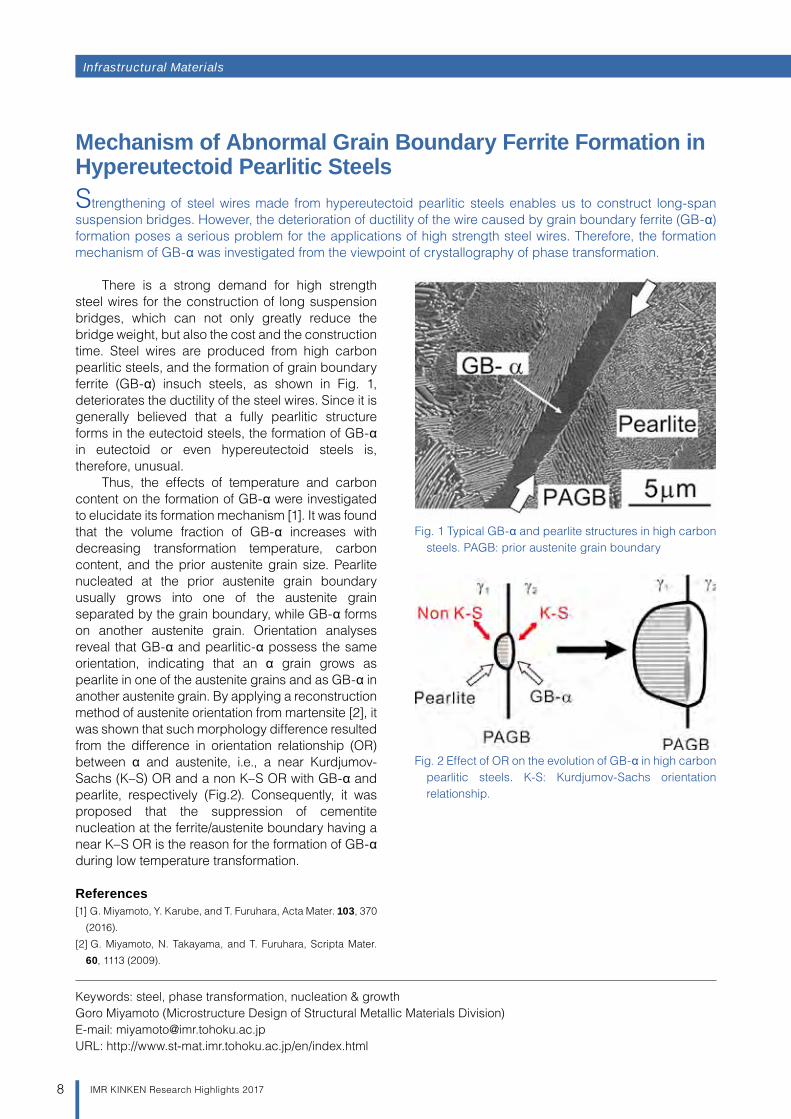
There is a strong demand for high strength steel wires for the construction of long suspension bridges, which can not only greatly reduce the bridge weight, but also the cost and the construction time. Steel wires are produced from high carbon pearlitic steels, and the formation of grain boundary ferrite (GB-α) insuch steels, as shown in Fig. 1, deteriorates the ductility of the steel wires. Since it is generally believed that a fully pearlitic structure forms in the eutectoid steels, the formation of GB-α in eutectoid or even hypereutectoid steels is, therefore, unusual.
Thus, the effects of temperature and carbon content on the formation of GB-α were investigated to elucidate its formation mechanism [1]. It was found that the volume fraction of GB-α increases with decreasing transformation temperature, carbon content, and the prior austenite grain size. Pearlite nucleated at the prior austenite grain boundary usually grows into one of the austenite grain separated by the grain boundary, while GB-α forms on another austenite grain. Orientation analyses reveal that GB-α and pearlitic-α possess the same orientation, indicating that an α grain grows as pearlite in one of the austenite grains and as GB-α in another austenite grain. By applying a reconstruction method of austenite orientation from martensite [2], it was shown that such morphology difference resulted from the difference in orientation relationship (OR) between α and austenite, i.e., a near Kurdjumov-Sachs (K–S) OR and a non K–S OR with GB-α and pearlite, respectively (Fig.2). Consequently, it was proposed that the suppression of cementite nucleation at the ferrite/austenite boundary having a near K–S OR is the reason for the formation of GB-α during low temperature transformation.
References[1] G. Miyamoto, Y. Karube, and T. Furuhara, Acta Mater. 103, 370
(2016).
[2] G. Miyamoto, N. Takayama, and T. Furuhara, Scripta Mater.
60, 1113 (2009).
Mechanism of Abnormal Grain Boundary Ferrite Formation in Hypereutectoid Pearlitic SteelsStrengthening of steel wires made from hypereutectoid pearlitic steels enables us to construct long-span suspension bridges. However, the deterioration of ductility of the wire caused by grain boundary ferrite (GB-α) formation poses a serious problem for the applications of high strength steel wires. Therefore, the formation mechanism of GB-α was investigated from the viewpoint of crystallography of phase transformation.
Keywords: steel, phase transformation, nucleation & growthGoro Miyamoto (Microstructure Design of Structural Metallic Materials Division)E-mail: [email protected]: http://www.st-mat.imr.tohoku.ac.jp/en/index.html
Fig. 1 Typical GB-α and pearlite structures in high carbon steels. PAGB: prior austenite grain boundary
Fig. 2 Effect of OR on the evolution of GB-α in high carbon pearlitic steels. K-S: Kurdjumov-Sachs orientation relationship.
Infrastructural Materials IMR KINKEN Research Highlights 2017
9IMR KINKEN Research Highlights 2017
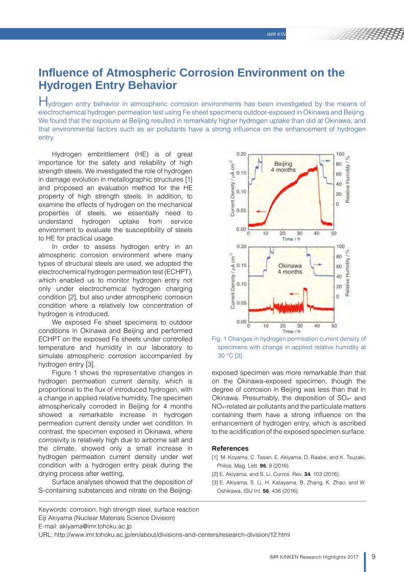
Hydrogen embrittlement (HE) is of great importance for the safety and reliability of high strength steels. We investigated the role of hydrogen in damage evolution in metallographic structures [1] and proposed an evaluation method for the HE property of high strength steels. In addition, to examine the effects of hydrogen on the mechanical properties of steels, we essentially need to understand hydrogen uptake from service environment to evaluate the susceptibility of steels to HE for practical usage.
In order to assess hydrogen entry in an atmospheric corrosion environment where many types of structural steels are used, we adopted the electrochemical hydrogen permeation test (ECHPT), which enabled us to monitor hydrogen entry not only under electrochemical hydrogen charging condition [2], but also under atmospheric corrosion condition where a relatively low concentration of hydrogen is introduced.
We exposed Fe sheet specimens to outdoor conditions in Okinawa and Beijing and performed ECHPT on the exposed Fe sheets under controlled temperature and humidity in our laboratory to simulate atmospheric corrosion accompanied by hydrogen entry [3].
Figure 1 shows the representative changes in hydrogen permeation current density, which is proportional to the flux of introduced hydrogen, with a change in applied relative humidity. The specimen atmospherically corroded in Beijing for 4 months showed a remarkable increase in hydrogen permeation current density under wet condition. In contrast, the specimen exposed in Okinawa, where corrosivity is relatively high due to airborne salt and the climate, showed only a small increase in hydrogen permeation current density under wet condition with a hydrogen entry peak during the drying process after wetting.
Surface analyses showed that the deposition of S-containing substances and nitrate on the Beijing-
exposed specimen was more remarkable than that on the Okinawa-exposed specimen, though the degree of corrosion in Beijing was less than that in Okinawa. Presumably, the deposition of SOx- and NOx-related air pollutants and the particulate matters containing them have a strong influence on the enhancement of hydrogen entry, which is ascribed to the acidification of the exposed specimen surface.
References[1] M. Koyama, C. Tasan, E. Akiyama, D. Raabe, and K. Tsuzaki,
Philos. Mag. Lett. 96, 9 (2016).
[2] E. Akiyama, and S. Li, Corros. Rev. 34, 103 (2016).
[3] E. Akiyama, S. Li, H. Katayama, B. Zhang, K. Zhao, and W.
Oshikawa, ISIJ Int. 56, 436 (2016).
Influence of Atmospheric Corrosion Environment on the Hydrogen Entry BehaviorHydrogen entry behavior in atmospheric corrosion environments has been investigated by the means of electrochemical hydrogen permeation test using Fe sheet specimens outdoor-exposed in Okinawa and Beijing. We found that the exposure at Beijing resulted in remarkably higher hydrogen uptake than did at Okinawa, and that environmental factors such as air pollutants have a strong influence on the enhancement of hydrogen entry.
Keywords: corrosion, high strength steel, surface reactionEiji Akiyama (Nuclear Materials Science Division)E-mail: [email protected]: http://www.imr.tohoku.ac.jp/en/about/divisions-and-centers/research-division/12.html
Fig. 1 Changes in hydrogen permeation current density of specimens with change in applied relative humidity at 30 °C [3].
Infrastructural Materials
10 IMR KINKEN Research Highlights 2017
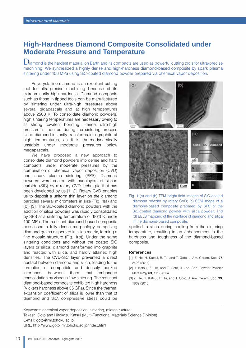
Polycrystalline diamond is an excellent cutting tool for ultra-precise machining because of its extraordinarily high hardness. Diamond compacts such as those in tipped tools can be manufactured by sintering under ultra-high pressures above several gigapascals and at high temperatures above 2500 K. To consolidate diamond powders, high sintering temperatures are necessary owing to its strong covalent bonding. Hence, ultra-high pressure is required during the sintering process since diamond instantly transforms into graphite at high temperatures, as it is thermodynamically unstable under moderate pressures below megapascals.
We have proposed a new approach to consolidate diamond powders into dense and hard compacts under moderate pressures by the combination of chemical vapor deposition (CVD) and spark plasma sintering (SPS). Diamond powders were coated with nanolayers of silicon carbide (SiC) by a rotary CVD technique that has been developed by us [1, 2]. Rotary CVD enables us to deposit a uniform thin layer on the diamond particles several micrometers in size (Fig. 1(a) and (b)) [3]. The SiC-coated diamond powders with the addition of silica powders was rapidly consolidated by SPS at a sintering temperature of 1873 K under 100 MPa. The resultant diamond-based composite possessed a fully dense morphology comprising diamond grains dispersed in silica matrix, forming a fine mosaic structure (Fig. 1(b)). Under the same sintering conditions and without the coated SiC layers or silica, diamond transformed into graphite and reacted with silica, and hardly attained high densities. The CVD-SiC layer prevented a direct contact between diamond and silica, leading to the formation of compatible and densely packed interfaces between them that enhanced consolidation by viscous flow sintering. The resultant diamond-based composite exhibited high hardness (Vickers hardness above 35 GPa). Since the thermal expansion coefficient of silica is lower than that of diamond and SiC, compressive stress could be
applied to silica during cooling from the sintering temperature, resulting in an enhancement in the hardness and toughness of the diamond-based composite.
References[1] Z. He, H. Katsui, R. Tu, and T. Goto, J. Am. Ceram. Soc. 97,
2423 (2014).
[2] H. Katsui, Z. He, and T. Goto, J. Jpn. Soc. Powder Powder
Metallurgy 63, 111 (2016).
[3] Z. He, H. Katsui, R. Tu, and T. Goto, J. Am. Ceram. Soc. 99,
1862 (2016).
High-Hardness Diamond Composite Consolidated under Moderate Pressure and TemperatureDiamond is the hardest material on Earth and its compacts are used as powerful cutting tools for ultra-precise machining. We synthesized a highly dense and high-hardness diamond-based composite by spark plasma sintering under 100 MPa using SiC-coated diamond powder prepared via chemical vapor deposition.
Keywords: chemical vapor deposition, sintering, microstructureTakashi Goto and Hirokazu Katsui (Multi-Functional Materials Science Division)E-mail: [email protected]: http://www.goto.imr.tohoku.ac.jp/index.html
Fig. 1 (a) and (b) TEM bright field images of SiC-coated diamond powder by rotary CVD; (c) SEM image of a diamond-based composite prepared by SPS of the SiC-coated diamond powder with silica powder; and (d) EELS mapping of the interface of diamond and silica in the diamond-based composite.
Infrastructural Materials IMR KINKEN Research Highlights 2017
11IMR KINKEN Research Highlights 2017
Twinning represents an important deformation mode in Mg alloys, which have a hexagonal close-packed (HCP) crystalline structure, because they do not have sufficient slip systems for continuous plastic deformation as in polycrystals. In general, twin in pure Mg and its alloys is not stable, and may either grow or shrink (detwin) under further deformation. For this reason, twin-boundary (TB) motion affects the performances of Mg alloys in many respects such as fatigue, strength, pseudoelasticity, and damping capacity [1].
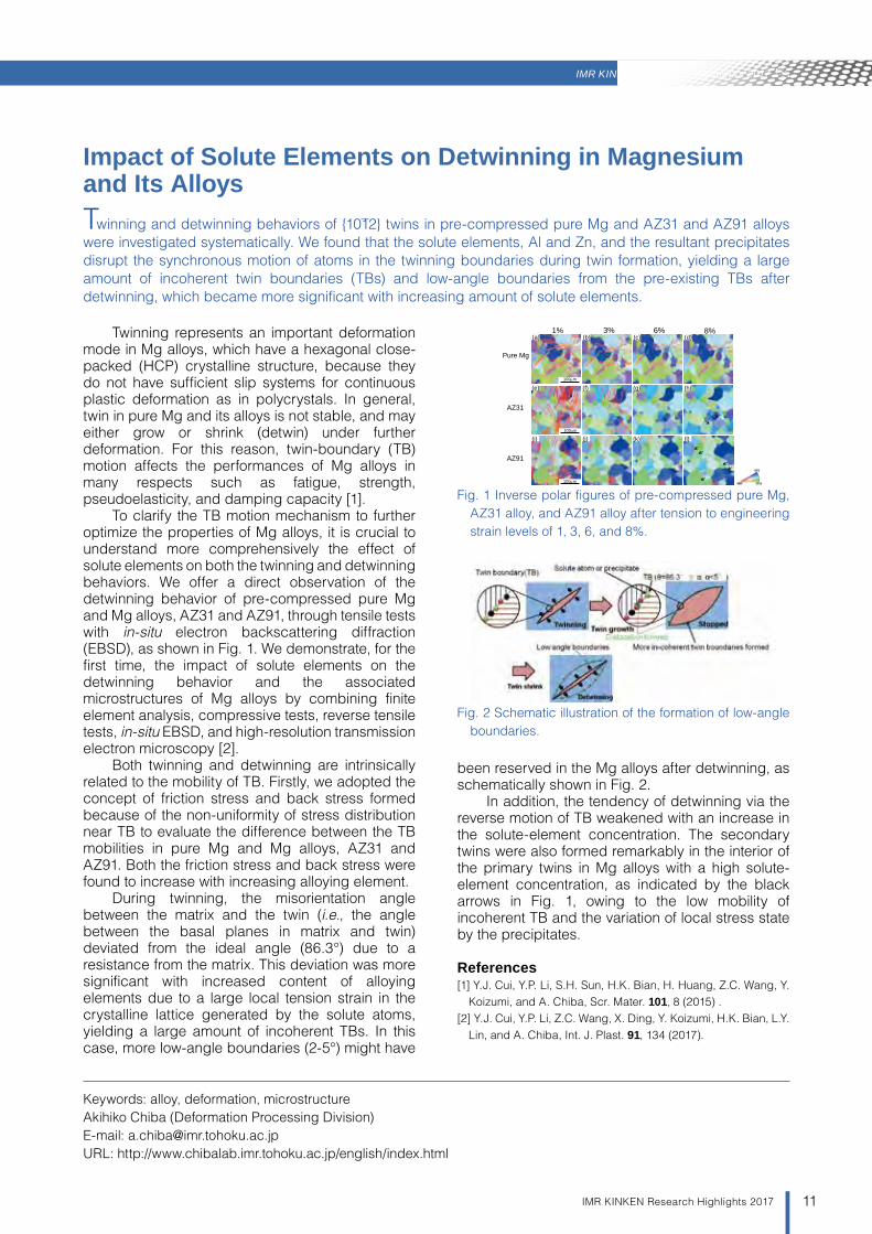
To clarify the TB motion mechanism to further optimize the properties of Mg alloys, it is crucial to understand more comprehensively the effect of solute elements on both the twinning and detwinning behaviors. We offer a direct observation of the detwinning behavior of pre-compressed pure Mg and Mg alloys, AZ31 and AZ91, through tensile tests with in-situ electron backscattering diffraction (EBSD), as shown in Fig. 1. We demonstrate, for the first time, the impact of solute elements on the detwinning behavior and the associated microstructures of Mg alloys by combining finite element analysis, compressive tests, reverse tensile tests, in-situ EBSD, and high-resolution transmission electron microscopy [2].
Both twinning and detwinning are intrinsically related to the mobility of TB. Firstly, we adopted the concept of friction stress and back stress formed because of the non-uniformity of stress distribution near TB to evaluate the difference between the TB mobilities in pure Mg and Mg alloys, AZ31 and AZ91. Both the friction stress and back stress were found to increase with increasing alloying element.
During twinning, the misorientation angle between the matrix and the twin (i.e., the angle between the basal planes in matrix and twin) deviated from the ideal angle (86.3°) due to a resistance from the matrix. This deviation was more significant with increased content of alloying elements due to a large local tension strain in the crystalline lattice generated by the solute atoms, yielding a large amount of incoherent TBs. In this case, more low-angle boundaries (2-5°) might have
been reserved in the Mg alloys after detwinning, as schematically shown in Fig. 2.
In addition, the tendency of detwinning via the reverse motion of TB weakened with an increase in the solute-element concentration. The secondary twins were also formed remarkably in the interior of the primary twins in Mg alloys with a high solute-element concentration, as indicated by the black arrows in Fig. 1, owing to the low mobility of incoherent TB and the variation of local stress state by the precipitates.
References[1] Y.J. Cui, Y.P. Li, S.H. Sun, H.K. Bian, H. Huang, Z.C. Wang, Y.
Koizumi, and A. Chiba, Scr. Mater. 101, 8 (2015) .[2] Y.J. Cui, Y.P. Li, Z.C. Wang, X. Ding, Y. Koizumi, H.K. Bian, L.Y.
Lin, and A. Chiba, Int. J. Plast. 91, 134 (2017).
Impact of Solute Elements on Detwinning in Magnesium and Its AlloysTwinning and detwinning behaviors of 1012 twins in pre-compressed pure Mg and AZ31 and AZ91 alloys were investigated systematically. We found that the solute elements, Al and Zn, and the resultant precipitates disrupt the synchronous motion of atoms in the twinning boundaries during twin formation, yielding a large amount of incoherent twin boundaries (TBs) and low-angle boundaries from the pre-existing TBs after detwinning, which became more significant with increasing amount of solute elements.
Keywords: alloy, deformation, microstructureAkihiko Chiba (Deformation Processing Division)E-mail: [email protected]: http://www.chibalab.imr.tohoku.ac.jp/english/index.html
Fig. 1 Inverse polar figures of pre-compressed pure Mg, AZ31 alloy, and AZ91 alloy after tension to engineering strain levels of 1, 3, 6, and 8%.
Fig. 2 Schematic illustration of the formation of low-angle boundaries.
Fig. 1 Inverse polar figures of pre-compressed pure Mg, AZ31 alloy, and AZ91 alloy after tension to engineering strain levels of 1, 3, 6, and 8%.
1%
Pure Mg
AZ31
AZ91
100mm
3% 6% 8%
100mm
100mm
(a) (b) (c) (d)
(e) (f) (g) (h)
(i) (j) (k) (l)
Infrastructural Materials
12 IMR KINKEN Research Highlights 2017
Even though the transformation behaviors during heat-treatments in aluminum (Al) alloys have been known for a long time, surprisingly, only a small amount of information was available on the commercial grade die-cast Al alloys because of the intrinsic two-phase nature of the alloys and the ubiquitous presence of defects such as porosity. With the advent of squeeze die-casting, it is now possible to manufacture die-cast Al alloys free from such imperfections and carry out conventional ageing. Here, we report the structural evolution of an Al alloy prepared through a newly developed squeeze die-casting technique, with a composition similar to that of JIS ADC12.
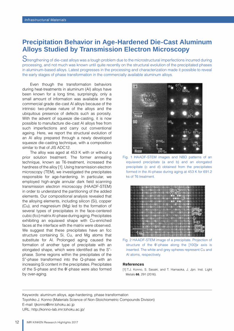
The alloy was aged at 453 K with or without a prior solution treatment. The former annealing technique, known as T6-treatment, increased the hardness of the alloy [1]. Using transmission electron microscopy (TEM), we investigated the precipitates responsible for age-hardening. In particular, we employed high-angle annular dark field scanning transmission electron microscopy (HAADF-STEM) in order to understand the partitioning of the added elements. Our compositional analysis revealed that the alloying elements, including silicon (Si), copper (Cu), and magnesium (Mg) led to the formation of several types of precipitates in the face-centered cubic (fcc) matrix Al-phase during aging. Precipitates exhibiting an equiaxed shape with Cu-enriched faces at the interface with the matrix were observed. We suggest that these precipitates have an fcc structure containing Si, Cu, and Mg atoms that substitute for Al. Prolonged aging caused the formation of another type of precipitate with an elongated shape, which were identified as the S”-phase. Some regions within the precipitates of the S”-phase transformed into the Q-phase with an increasing Si content in the precipitates. Precipitates of the S-phase and the θ’-phase were also formed by over-aging.
References[1] T.J. Konno, S. Sasaki, and T. Hamaoka, J. Jpn. Inst. Light
Metals 66, 291 (2016).
Precipitation Behavior in Age-Hardened Die-Cast Aluminum Alloys Studied by Transmission Electron MicroscopyStrengthening of die-cast alloys was a tough problem due to the microstructural imperfections incurred during processing, and not much was known until quite recently on the structural evolution of the precipitated phases in aluminum-based alloys. Latest progresses in the processing and characterization made it possible to reveal the early stages of phase transformation in the commercially available aluminum alloys.
Keywords: aluminum alloys, age-hardening, phase transformationToyohiko J. Konno (Materials Science of Non-Stoichiometric Compounds Division)E-mail: [email protected]: http://konno-lab.imr.tohoku.ac.jp/
Fig. 1 HAADF-STEM images and NBD patterns of an equiaxed precipitate (a and b) and an elongated precipitate (c and d) obtained from the precipitates formed in the Al-phase during aging at 453 K for 691.2 ks of T6 treatment.
Fig. 2 HAADF-STEM image of a precipitate. Projection of structure of the θ’-phase along the [100]θ’ axis is inserted. The white and grey spheres represent Cu and Al atoms, respectively.
Infrastructural Materials IMR KINKEN Research Highlights 2017
13IMR KINKEN Research Highlights 2017
Alumina inclusions contaminate steel products mainly during the process of deoxidation and are known to deteriorate the performance of the steel products. The size of these inclusions should be controlled around 5~40 micrometer diameter. The diameter, number, and distribution of these inclusions are evaluated according to the JIS G 0555 standard, “Microscopic testing method for the non-metallic inclusions in steel”. However, this method is based on visual counting using an optical microscope and tends to be tedious and time consuming. Considering these situations, we adopted laser-induced breakdown spectroscopy (LIBS) to detect alumina particles and their distribution in ferric stainless steels. The principal of LIBS is as follows: when a pulsed laser with high energy density is focused onto the surface of a specimen, the atoms in that spot receive energy from the laser and is ablated into a laser plasma. Inside the laser plasma, the ablated atoms/ions are excited/de-excited and results in an optical emission. In this study, a small plate of ferric stainless steel was placed on the LIBS system described below, and alumina inclusions were detected by LIBS with real-time monitoring of the surface of the specimen.
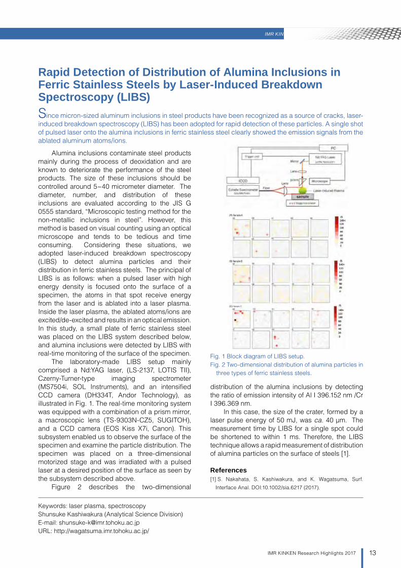
The laboratory-made LIBS setup mainly comprised a Nd:YAG laser, (LS-2137, LOTIS TII), Czerny-Turner-type imaging spectrometer (MS7504i, SOL Instruments), and an intensified CCD camera (DH334T, Andor Technology), as illustrated in Fig. 1. The real-time monitoring system was equipped with a combination of a prism mirror, a macroscopic lens (TS-9303N-CZ5, SUGITOH), and a CCD camera (EOS Kiss X7i, Canon). This subsystem enabled us to observe the surface of the specimen and examine the particle distribution. The specimen was placed on a three-dimensional motorized stage and was irradiated with a pulsed laser at a desired position of the surface as seen by the subsystem described above.
Figure 2 describes the two-dimensional
distribution of the alumina inclusions by detecting the ratio of emission intensity of Al I 396.152 nm /Cr I 396.369 nm.
In this case, the size of the crater, formed by a laser pulse energy of 50 mJ, was ca. 40 μm. The measurement time by LIBS for a single spot could be shortened to within 1 ms. Therefore, the LIBS technique allows a rapid measurement of distribution of alumina particles on the surface of steels [1].
References[1] S. Nakahata, S. Kashiwakura, and K. Wagatsuma, Surf.
Interface Anal. DOI:10.1002/sia.6217 (2017).
Rapid Detection of Distribution of Alumina Inclusions in Ferric Stainless Steels by Laser-Induced Breakdown Spectroscopy (LIBS)Since micron-sized aluminum inclusions in steel products have been recognized as a source of cracks, laser-induced breakdown spectroscopy (LIBS) has been adopted for rapid detection of these particles. A single shot of pulsed laser onto the alumina inclusions in ferric stainless steel clearly showed the emission signals from the ablated aluminum atoms/ions.
Keywords: laser plasma, spectroscopyShunsuke Kashiwakura (Analytical Science Division)E-mail: [email protected]: http://wagatsuma.imr.tohoku.ac.jp/
Fig. 1 Block diagram of LIBS setup.Fig. 2 Two-dimensional distribution of alumina particles in
three types of ferric stainless steels.


Energy-related Materials
IMR KINKEN Research Highlights 2017Research
16 IMR KINKEN Research Highlights 2017
Energy-related Materials
Multicrystalline Si (mc-Si) ingots, grown by directional solidification for use in solar cells, always exhibit twin boundaries. However, the underlying reason for its occurrence is not well understood.
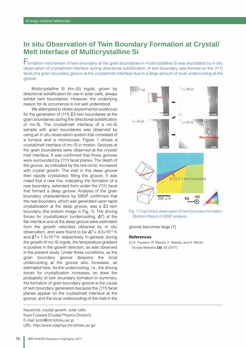
We attempted to obtain experimental evidences for the generation of 111 Σ3 twin boundaries at the grain boundaries during the directional solidification of mc-Si. The crystal/melt interface of a mc-Si sample with grain boundaries was observed by using an in situ observation system that consisted of a furnace and a microscope. Figure 1 shows a crystal/melt interface of mc-Si in motion. Grooves at the grain boundaries were observed at the crystal/melt interface. It was confirmed that those grooves were surrounded by 111 facet planes. The depth of the groove, as indicated by the red circle, increased with crystal growth. The melt in this deep groove then rapidly crystalized, filling the groove. It was noted that a new line, indicating the formation of a new boundary, extended from under the 111 facet that formed a deep groove. Analysis of the grain boundary characteristics by EBSP confirmed that the new boundary, which was generated upon rapid crystallization at the deep groove, was a Σ3 twin boundary (the bottom image in Fig. 1). The driving forces for crystallization (undercooling, ΔT) at the flat interface and at the deep groove were estimated from the growth velocities obtained by in situ observation, and were found to be ΔT ≈ 9.5×10⁻⁵ K and ΔT ≈ 1.3×10⁻³ K, respectively. In general, during the growth of mc-Si ingots, the temperature gradient is positive in the growth direction, as was observed in the present study. Under these conditions, as the grain boundary groove deepens the local undercooling at the groove also increases, as estimated here. As the undercooling, i.e., the driving forces for crystallization increases, so does the probability of twin boundary formation.In summary, the formation of grain boundary groove is the cause of twin boundary generation because the 111 facet planes appear on the crystal/melt interface at the groove, and the local undercooling of the melt in the
groove becomes large [1].
References[1] K. Fujiwara, R. Maeda, K. Maeda, and H. Morito,
Scripta Matrialia 133, 65 (2017).
In situ Observation of Twin Boundary Formation at Crystal/Melt Interface of Multicrystalline SiFormation mechanism of twin boundary at the grain boundaries in multicrystalline Si was elucidated by in situ observation of crystal/melt interface during directional solidification. A twin boundary was formed on the 111 facet of a grain-boundary groove at the crystal/melt interface due to a large amount of local undercooling at the groove.
Keywords: crystal growth, solar cellsKozo Fujiwara (Crystal Physics Division)E-mail: [email protected]: http://www.xtalphys.imr.tohoku.ac.jp/
Fig. 1 (Top) Direct observation of twin boundary formation. (Bottom) Result of EBSP analysis.
17IMR KINKEN Research Highlights 2017
Energy-related Materials IMR KINKEN Research Highlights 2017
Grain boundaries (GBs) in Si ingots that are used for solar cells have serious impacts on the solar cell efficiency owing to the segregation of detrimental impurity atoms. Impurity atoms such as oxygen and transition metals are introduced during crystal growth and cell processing, depending on the structural conditions at GBs. A precise understanding of the segregation mechanism is an important issue for the production of cost-effective solar cells by engineering the structural condition of the impurities segregating at GBs.
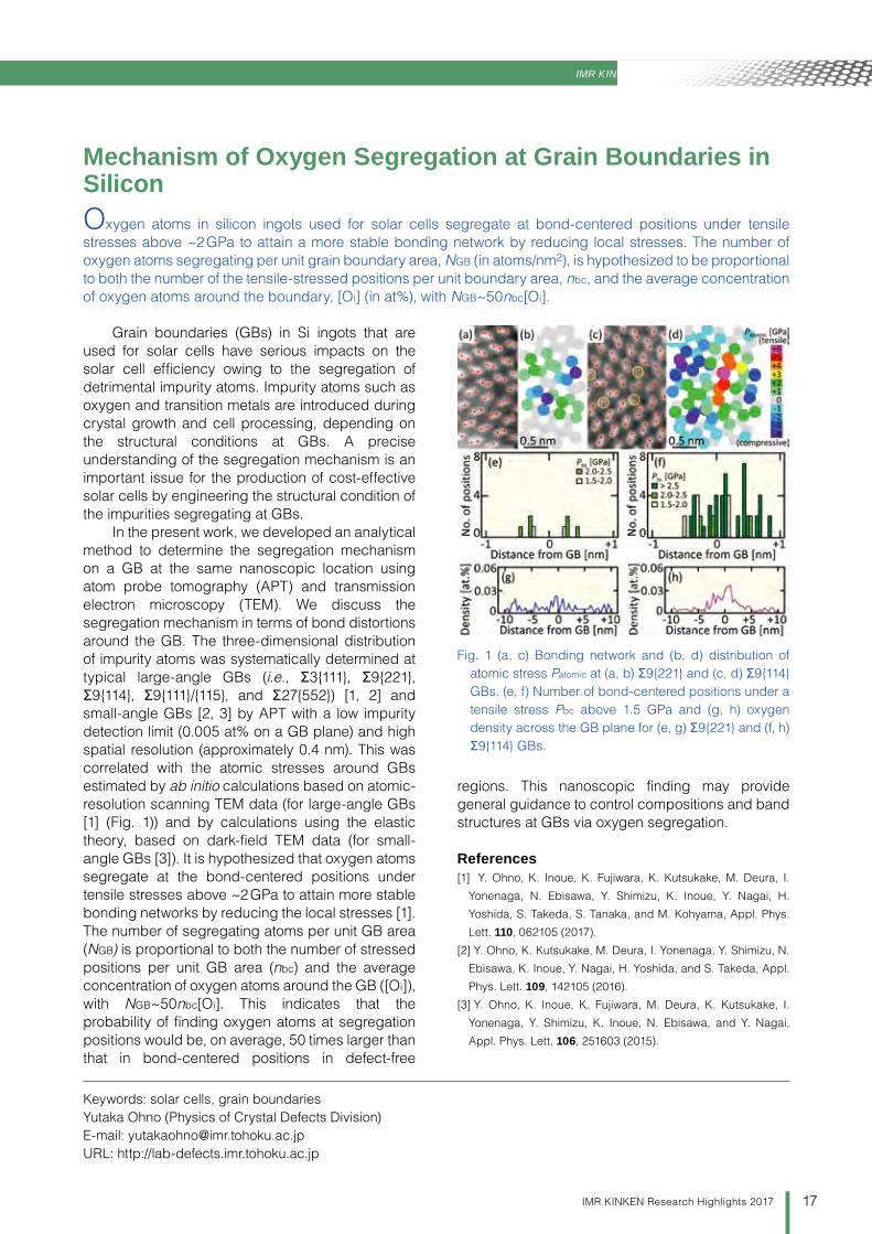
In the present work, we developed an analytical method to determine the segregation mechanism on a GB at the same nanoscopic location using atom probe tomography (APT) and transmission electron microscopy (TEM). We discuss the segregation mechanism in terms of bond distortions around the GB. The three-dimensional distribution of impurity atoms was systematically determined at typical large-angle GBs (i.e., Σ3111, Σ9221, Σ9114, Σ9111/115, and Σ27552) [1, 2] and small-angle GBs [2, 3] by APT with a low impurity detection limit (0.005 at% on a GB plane) and high spatial resolution (approximately 0.4 nm). This was correlated with the atomic stresses around GBs estimated by ab initio calculations based on atomic-resolution scanning TEM data (for large-angle GBs [1] (Fig. 1)) and by calculations using the elastic theory, based on dark-field TEM data (for small-angle GBs [3]). It is hypothesized that oxygen atoms segregate at the bond-centered positions under tensile stresses above ~2 GPa to attain more stable bonding networks by reducing the local stresses [1]. The number of segregating atoms per unit GB area (NGB) is proportional to both the number of stressed positions per unit GB area (nbc) and the average concentration of oxygen atoms around the GB ([Oi]), with NGB~50nbc[Oi]. This indicates that the probability of finding oxygen atoms at segregation positions would be, on average, 50 times larger than that in bond-centered positions in defect-free
regions. This nanoscopic finding may provide general guidance to control compositions and band structures at GBs via oxygen segregation.
References[1] Y. Ohno, K. Inoue, K. Fujiwara, K. Kutsukake, M. Deura, I.
Yonenaga, N. Ebisawa, Y. Shimizu, K. Inoue, Y. Nagai, H.
Yoshida, S. Takeda, S. Tanaka, and M. Kohyama, Appl. Phys.
Lett. 110, 062105 (2017).
[2] Y. Ohno, K. Kutsukake, M. Deura, I. Yonenaga, Y. Shimizu, N.
Ebisawa, K. Inoue, Y. Nagai, H. Yoshida, and S. Takeda, Appl.
Phys. Lett. 109, 142105 (2016).
[3] Y. Ohno, K. Inoue, K. Fujiwara, M. Deura, K. Kutsukake, I.
Yonenaga, Y. Shimizu, K. Inoue, N. Ebisawa, and Y. Nagai,
Appl. Phys. Lett. 106, 251603 (2015).
Mechanism of Oxygen Segregation at Grain Boundaries in SiliconOxygen atoms in silicon ingots used for solar cells segregate at bond-centered positions under tensile stresses above ~2 GPa to attain a more stable bonding network by reducing local stresses. The number of oxygen atoms segregating per unit grain boundary area, NGB (in atoms/nm2), is hypothesized to be proportional to both the number of the tensile-stressed positions per unit boundary area, nbc, and the average concentration of oxygen atoms around the boundary, [Oi] (in at%), with NGB~50nbc[Oi].
Keywords: solar cells, grain boundariesYutaka Ohno (Physics of Crystal Defects Division)E-mail: [email protected]: http://lab-defects.imr.tohoku.ac.jp
Fig. 1 (a, c) Bonding network and (b, d) distribution of atomic stress Patomic at (a, b) Σ9221 and (c, d) Σ9114 GBs. (e, f) Number of bond-centered positions under a tensile stress Pbc above 1.5 GPa and (g, h) oxygen density across the GB plane for (e, g) Σ9221 and (f, h) Σ9114 GBs.
18 IMR KINKEN Research Highlights 2017
Energy-related Materials
High-functional and high-performance materials are necessary in a wide variety of research fields such as fuel cell, electronics, tribology, etc., for solving the energy and environmental problems and for the development of super-precision systems. Currently, a deep understanding of multi-physics phenomena, including chemical reactions, friction, impact, fluid, heat etc, is required for materials design. However, traditional simulation methods such as first-principles calculations and fluid mechanics cannot simulate the abovementioned multi-physics phenomena. Therefore, we applied our multi-physics simulator based on molecular dynamics, tight-binding quantum chemical molecular dynamics, etc., for pioneering next-generation materials design [1-2].
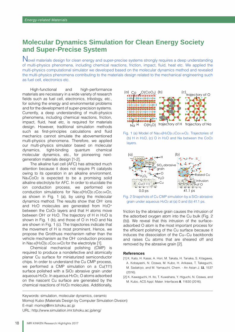
The alkaline fuel cell (AFC) has attracted much attention because it does not require Pt catalysts owing to its operation in an alkaline environment. NaxCoO2 is expected to be a promising solid alkaline electrolyte for AFC. In order to elucidate the ion conduction process, we performed ion conduction simulations for Na0.6(H3O)0.2Co0.94O2, as shown in Fig. 1 (a), by using the molecular dynamics method. The results show that OH- ions and H2O molecules are generated from H3O+ between the CoO2 layers and that H atoms move between OH- or H2O. The trajectory of H in H3O is shown in Fig. 1 (b), and those of O in H3O and Na are shown in Fig. 1 (c). The trajectories indicate that the movement of H is most prominent. Hence, we propose the Grotthuss mechanism rather than the vehicle mechanism as the OH- conduction process in Na0.6(H3O)0.2Co0.94O2 for the electrolyte [1].
Chemical mechanical polishing (CMP) is required to produce a nondefective and atomically planar Cu surface for miniaturized semiconductor chips. In order to understand the Cu CMP process, we performed a CMP simulation on a Cu(111) surface polished with a SiO2 abrasive grain under aqueous H2O2. In aqueous H2O2, O atoms adsorbed on the nascent Cu surface are generated by the chemical reactions of H2O2 molecules. Additionally,
friction by the abrasive grain causes the intrusion of the adsorbed oxygen atom into the Cu bulk (Fig. 2 (b)). We reveal that this intrusion of the surface-adsorbed O atom is the most important process for the efficient polishing of the Cu surface because it induces the dissociation of the Cu−Cu backbonds and raises Cu atoms that are sheared off and removed by the abrasive grain [2].
References[1] K. Kato, H. Kasai, A. Hori, M. Takata, H. Tanaka, S. Kitagawa,
A. Kobayashi, N. Ozawa, M. Kubo, H. Arikawa, T. Takeguchi,
M. Sadakiyo, and M. Yamauchi, Chem. - An Asian J. 11, 1537
(2016).
[2] K. Kawaguchi, H. Ito, T. Kuwahara, Y. Higuchi, N. Ozawa, and
M. Kubo, ACS Appl. Mater. Interfaces 8, 11830 (2016).
Molecular Dynamics Simulation for Clean Energy Society and Super-Precise SystemNovel materials design for clean energy and super-precise systems strongly requires a deep understanding of multi-physics phenomena, including chemical reactions, friction, impact, fluid, heat etc. We applied the multi-physics computational simulator we developed based on the molecular dynamics method and revealed the multi-physics phenomena contributing to the materials design related to the mechanical engineering such as fuel cell, electronics etc.
Keywords: simulation, molecular dynamics, ceramicMomoji Kubo (Materials Design by Computer Simulation Divsion)E-mail: [email protected]: http://www.simulation.imr.tohoku.ac.jp/eng/
Fig. 1 (a) Model of Na0.6(H3O)0.2Co0.94O2. Trajectories of (b) H in H3O, (c) O in H3O and Na between the CoO2 layers.
Fig. 2 Snapshots of Cu CMP simulation by a SiO2 abrasive grain under aqueous H2O2 at (a) 0 and (b) 41.1 ps.
(c)trajectory of O
trajectory of Na
(b)
trajectory of H
(a)
O(H3O)Na
O(CoO2)
H
Co
0.0 ps 41.1 ps
H2O2Raised Cu
SlidingLoad
(b)(a)
Cu(111)
H2O
SiO2 abrasive grain
Intrusionof OCu
Si
O
H
19IMR KINKEN Research Highlights 2017
Energy-related Materials IMR KINKEN Research Highlights 2017
Self-interstitial atom (SIA) clusters perform one-dimensional (1D) migration, i.e., a gliding motion along the Burgers vector with low activation energy. In a recent theory on defect structural evolution under high-energy neutron irradiation, 1D migration is regarded as a potential mechanism for controlling the kinetics of the defect reactions: e.g., void swelling and heterogeneous defect distribution near dislocations and grain boundaries. 1D migration is therefore of practical and fundamental importance in relation to nuclear materials research.
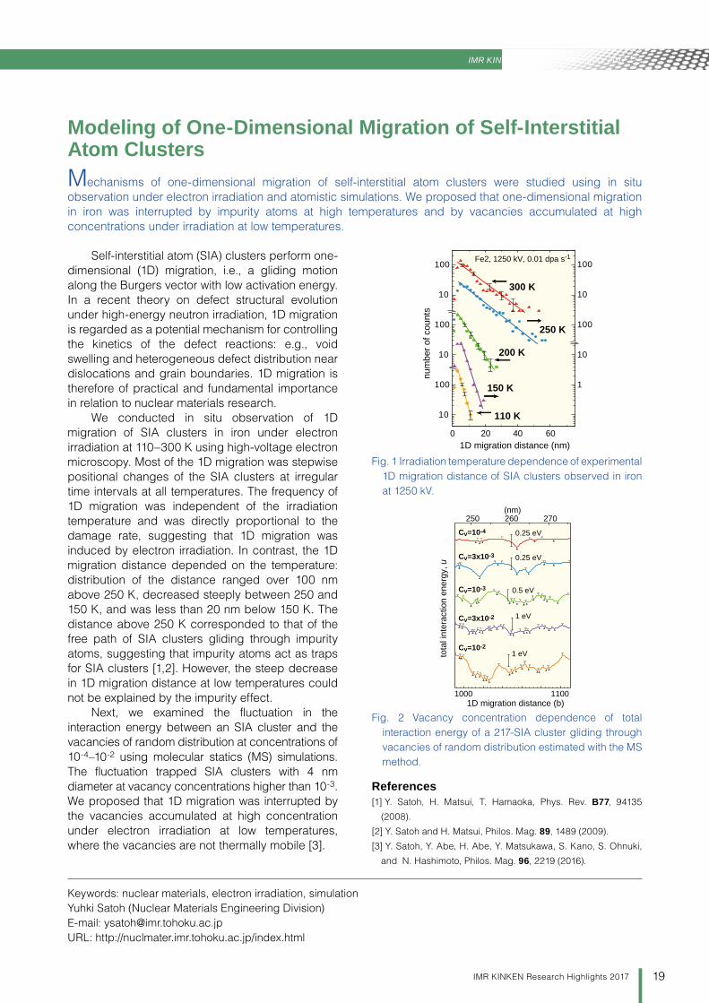
We conducted in situ observation of 1D migration of SIA clusters in iron under electron irradiation at 110–300 K using high-voltage electron microscopy. Most of the 1D migration was stepwise positional changes of the SIA clusters at irregular time intervals at all temperatures. The frequency of 1D migration was independent of the irradiation temperature and was directly proportional to the damage rate, suggesting that 1D migration was induced by electron irradiation. In contrast, the 1D migration distance depended on the temperature: distribution of the distance ranged over 100 nm above 250 K, decreased steeply between 250 and 150 K, and was less than 20 nm below 150 K. The distance above 250 K corresponded to that of the free path of SIA clusters gliding through impurity atoms, suggesting that impurity atoms act as traps for SIA clusters [1,2]. However, the steep decrease in 1D migration distance at low temperatures could not be explained by the impurity effect.
Next, we examined the fluctuation in the interaction energy between an SIA cluster and the vacancies of random distribution at concentrations of 10-4–10-2 using molecular statics (MS) simulations. The fluctuation trapped SIA clusters with 4 nm diameter at vacancy concentrations higher than 10-3. We proposed that 1D migration was interrupted by the vacancies accumulated at high concentration under electron irradiation at low temperatures, where the vacancies are not thermally mobile [3].
References[1] Y. Satoh, H. Matsui, T. Hamaoka, Phys. Rev. B77, 94135
(2008).
[2] Y. Satoh and H. Matsui, Philos. Mag. 89, 1489 (2009).
[3] Y. Satoh, Y. Abe, H. Abe, Y. Matsukawa, S. Kano, S. Ohnuki,
and N. Hashimoto, Philos. Mag. 96, 2219 (2016).
Modeling of One-Dimensional Migration of Self-Interstitial Atom ClustersMechanisms of one-dimensional migration of self-interstitial atom clusters were studied using in situ observation under electron irradiation and atomistic simulations. We proposed that one-dimensional migration in iron was interrupted by impurity atoms at high temperatures and by vacancies accumulated at high concentrations under irradiation at low temperatures.
Keywords: nuclear materials, electron irradiation, simulationYuhki Satoh (Nuclear Materials Engineering Division)E-mail: [email protected]: http://nuclmater.imr.tohoku.ac.jp/index.html
Fig. 1 Irradiation temperature dependence of experimental 1D migration distance of SIA clusters observed in iron at 1250 kV.
Fig. 2 Vacancy concentration dependence of total interaction energy of a 217-SIA cluster gliding through vacancies of random distribution estimated with the MS method.
0 20 40 60
100
10
100
10
100
10nu
mbe
r of
cou
nts
100
10
100
10
1
300 K
250 K
200 K
150 K
110 K
Fe2, 1250 kV, 0.01 dpa s-1
1D migration distance (nm)
0.25 eV
0.25 eV
0.5 eV
1 eV
1 eV
1000 11001D migration distance (b)
250 260 270(nm)
tota
l int
erac
tion
ener
gy, u
Cv=10-4
Cv=3x10⁻³
Cv=10-3
Cv=3x10⁻²
Cv=10-2
20 IMR KINKEN Research Highlights 2017
Energy-related Materials
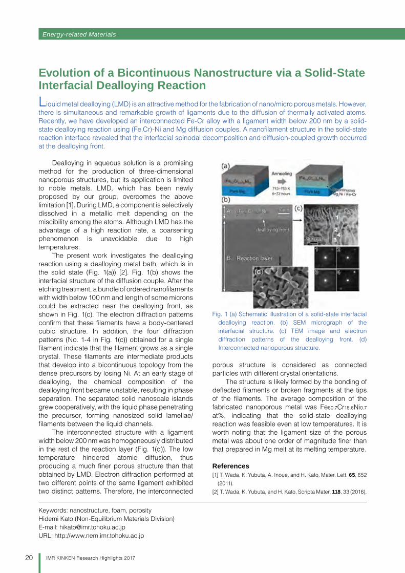
Dealloying in aqueous solution is a promising method for the production of three-dimensional nanoporous structures, but its application is limited to noble metals. LMD, which has been newly proposed by our group, overcomes the above limitation [1]. During LMD, a component is selectively dissolved in a metallic melt depending on the miscibility among the atoms. Although LMD has the advantage of a high reaction rate, a coarsening phenomenon is unavoidable due to high temperatures.
The present work investigates the dealloying reaction using a dealloying metal bath, which is in the solid state (Fig. 1(a)) [2]. Fig. 1(b) shows the interfacial structure of the diffusion couple. After the etching treatment, a bundle of ordered nanofilaments with width below 100 nm and length of some microns could be extracted near the dealloying front, as shown in Fig. 1(c). The electron diffraction patterns confirm that these filaments have a body-centered cubic structure. In addition, the four diffraction patterns (No. 1-4 in Fig. 1(c)) obtained for a single filament indicate that the filament grows as a single crystal. These filaments are intermediate products that develop into a bicontinuous topology from the dense precursors by losing Ni. At an early stage of dealloying, the chemical composition of the dealloying front became unstable, resulting in phase separation. The separated solid nanoscale islands grew cooperatively, with the liquid phase penetrating the precursor, forming nanosized solid lamellae/filaments between the liquid channels.
The interconnected structure with a ligament width below 200 nm was homogeneously distributed in the rest of the reaction layer (Fig. 1(d)). The low temperature hindered atomic diffusion, thus producing a much finer porous structure than that obtained by LMD. Electron diffraction performed at two different points of the same ligament exhibited two distinct patterns. Therefore, the interconnected
porous structure is considered as connected particles with different crystal orientations.
The structure is likely formed by the bonding of deflected filaments or broken fragments at the tips of the filaments. The average composition of the fabricated nanoporous metal was Fe80.7Cr18.6Ni0.7 at%, indicating that the solid-state dealloying reaction was feasible even at low temperatures. It is worth noting that the ligament size of the porous metal was about one order of magnitude finer than that prepared in Mg melt at its melting temperature.
References[1] T. Wada, K. Yubuta, A. Inoue, and H. Kato, Mater. Lett. 65, 652
(2011).
[2] T. Wada, K. Yubuta, and H. Kato, Scripta Mater. 118, 33 (2016).
Evolution of a Bicontinuous Nanostructure via a Solid-State Interfacial Dealloying ReactionLiquid metal dealloying (LMD) is an attractive method for the fabrication of nano/micro porous metals. However, there is simultaneous and remarkable growth of ligaments due to the diffusion of thermally activated atoms. Recently, we have developed an interconnected Fe-Cr alloy with a ligament width below 200 nm by a solid-state dealloying reaction using (Fe,Cr)-Ni and Mg diffusion couples. A nanofilament structure in the solid-state reaction interface revealed that the interfacial spinodal decomposition and diffusion-coupled growth occurred at the dealloying front.
Keywords: nanostructure, foam, porosityHidemi Kato (Non-Equilibrium Materials Division)E-mail: [email protected]: http://www.nem.imr.tohoku.ac.jp
Fig. 1 (a) Schematic illustration of a solid-state interfacial dealloying reaction. (b) SEM micrograph of the interfacial structure. (c) TEM image and electron diffraction patterns of the dealloying front. (d) Interconnected nanoporous structure.
21IMR KINKEN Research Highlights 2017
Energy-related Materials IMR KINKEN Research Highlights 2017
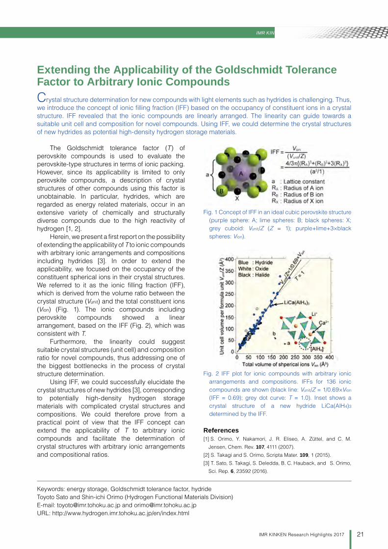
The Goldschmidt tolerance factor (T) of perovskite compounds is used to evaluate the perovskite-type structures in terms of ionic packing. However, since its applicability is limited to only perovskite compounds, a description of crystal structures of other compounds using this factor is unobtainable. In particular, hydrides, which are regarded as energy related materials, occur in an extensive variety of chemically and structurally diverse compounds due to the high reactivity of hydrogen [1, 2].
Herein, we present a first report on the possibility of extending the applicability of T to ionic compounds with arbitrary ionic arrangements and compositions including hydrides [3]. In order to extend the applicability, we focused on the occupancy of the constituent spherical ions in their crystal structures. We referred to it as the ionic filling fraction (IFF), which is derived from the volume ratio between the crystal structure (Vunit) and the total constituent ions (Vion) (Fig. 1). The ionic compounds including perovskite compounds showed a linear arrangement, based on the IFF (Fig. 2), which was consistent with T.
Furthermore, the linearity could suggest suitable crystal structures (unit cell) and composition ratio for novel compounds, thus addressing one of the biggest bottlenecks in the process of crystal structure determination.
Using IFF, we could successfully elucidate the crystal structures of new hydrides [3], corresponding to potentially high-density hydrogen storage materials with complicated crystal structures and compositions. We could therefore prove from a practical point of view that the IFF concept can extend the applicability of T to arbitrary ionic compounds and facilitate the determination of crystal structures with arbitrary ionic arrangements and compositional ratios.
References[1] S. Orimo, Y. Nakamori, J. R. Eliseo, A. Züttel, and C. M.
Jensen, Chem. Rev. 107, 4111 (2007).
[2] S. Takagi and S. Orimo, Scripta Mater. 109, 1 (2015).
[3] T. Sato, S. Takagi, S. Deledda, B. C. Hauback, and S. Orimo,
Sci. Rep. 6, 23592 (2016).
Extending the Applicability of the Goldschmidt Tolerance Factor to Arbitrary Ionic CompoundsCrystal structure determination for new compounds with light elements such as hydrides is challenging. Thus, we introduce the concept of ionic filling fraction (IFF) based on the occupancy of constituent ions in a crystal structure. IFF revealed that the ionic compounds are linearly arranged. The linearity can guide towards a suitable unit cell and composition for novel compounds. Using IFF, we could determine the crystal structures of new hydrides as potential high-density hydrogen storage materials.
Keywords: energy storage, Goldschmidt tolerance factor, hydrideToyoto Sato and Shin-ichi Orimo (Hydrogen Functional Materials Division)E-mail: [email protected] and [email protected]: http://www.hydrogen.imr.tohoku.ac.jp/en/index.html
Fig. 1 Concept of IFF in an ideal cubic perovskite structure (purple sphere: A; lime spheres: B; black spheres: X; grey cuboid: Vunit/Z (Z = 1); purple+lime+3×black spheres: Vion).
Fig. 2 IFF plot for ionic compounds with arbitrary ionic arrangements and compositions. IFFs for 136 ionic compounds are shown (black line: Vunit/Z = 1/0.69×Vion (IFF = 0.69); grey dot curve: T = 1.0). Inset shows a crystal structure of a new hydride LiCa(AlH4)3 determined by the IFF.
22 IMR KINKEN Research Highlights 2017
Energy-related Materials
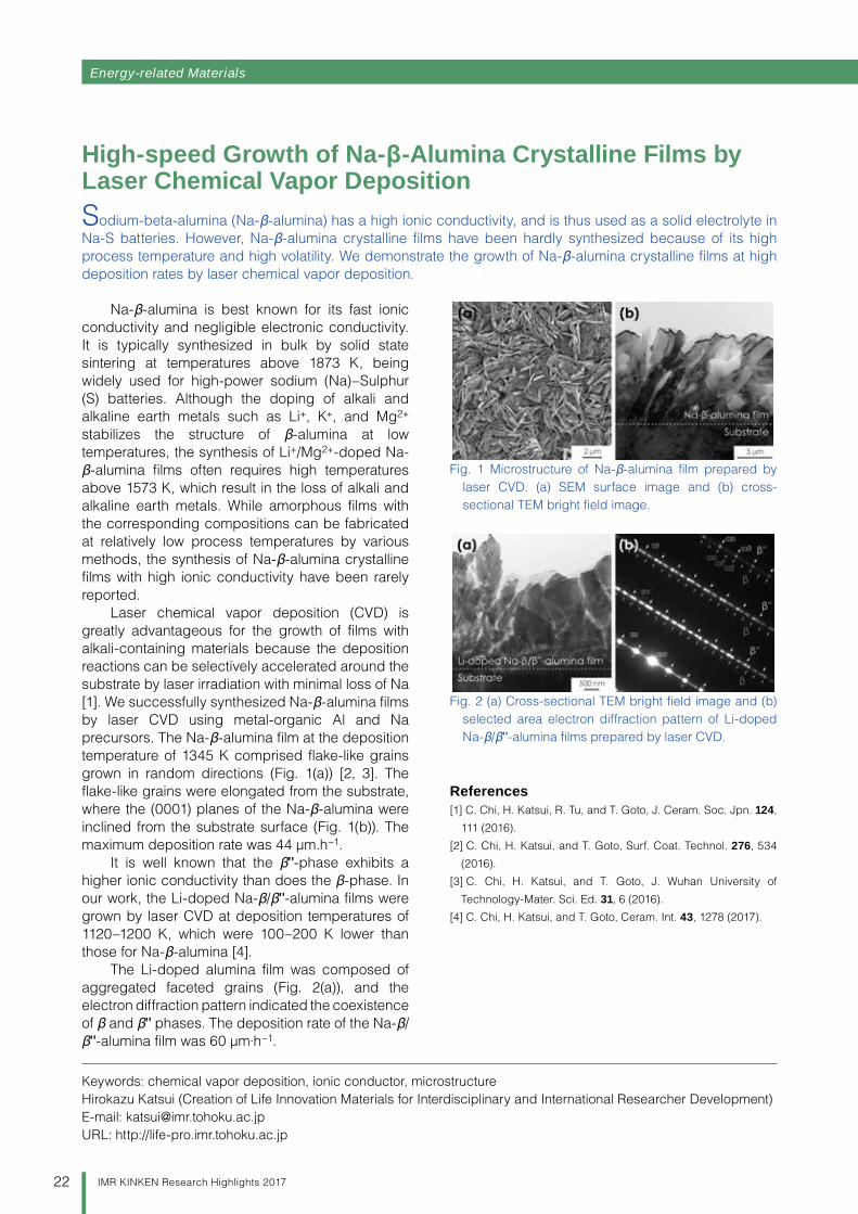
Na-β-alumina is best known for its fast ionic conductivity and negligible electronic conductivity. It is typically synthesized in bulk by solid state sintering at temperatures above 1873 K, being widely used for high-power sodium (Na)–Sulphur (S) batteries. Although the doping of alkali and alkaline earth metals such as Li+, K+, and Mg2+ stabilizes the structure of β-alumina at low temperatures, the synthesis of Li+/Mg2+-doped Na-β-alumina films often requires high temperatures above 1573 K, which result in the loss of alkali and alkaline earth metals. While amorphous films with the corresponding compositions can be fabricated at relatively low process temperatures by various methods, the synthesis of Na-β-alumina crystalline films with high ionic conductivity have been rarely reported.
Laser chemical vapor deposition (CVD) is greatly advantageous for the growth of films with alkali-containing materials because the deposition reactions can be selectively accelerated around the substrate by laser irradiation with minimal loss of Na [1]. We successfully synthesized Na-β-alumina films by laser CVD using metal-organic Al and Na precursors. The Na-β-alumina film at the deposition temperature of 1345 K comprised flake-like grains grown in random directions (Fig. 1(a)) [2, 3]. The flake-like grains were elongated from the substrate, where the (0001) planes of the Na-β-alumina were inclined from the substrate surface (Fig. 1(b)). The maximum deposition rate was 44 μm.h−1.
It is well known that the βʹʹ-phase exhibits a higher ionic conductivity than does the β-phase. In our work, the Li-doped Na-β/βʹʹ-alumina films were grown by laser CVD at deposition temperatures of 1120–1200 K, which were 100–200 K lower than those for Na-β-alumina [4].
The Li-doped alumina film was composed of aggregated faceted grains (Fig. 2(a)), and the electron diffraction pattern indicated the coexistence of β and βʹʹ phases. The deposition rate of the Na-β/βʹʹ-alumina film was 60 μm·h−1.
References[1] C. Chi, H. Katsui, R. Tu, and T. Goto, J. Ceram. Soc. Jpn. 124,
111 (2016).
[2] C. Chi, H. Katsui, and T. Goto, Surf. Coat. Technol. 276, 534
(2016).
[3] C. Chi, H. Katsui, and T. Goto, J. Wuhan University of
Technology-Mater. Sci. Ed. 31, 6 (2016).
[4] C. Chi, H. Katsui, and T. Goto, Ceram. Int. 43, 1278 (2017).
High-speed Growth of Na-β-Alumina Crystalline Films by Laser Chemical Vapor DepositionSodium-beta-alumina (Na-β-alumina) has a high ionic conductivity, and is thus used as a solid electrolyte in Na-S batteries. However, Na-β-alumina crystalline films have been hardly synthesized because of its high process temperature and high volatility. We demonstrate the growth of Na-β-alumina crystalline films at high deposition rates by laser chemical vapor deposition.
Keywords: chemical vapor deposition, ionic conductor, microstructureHirokazu Katsui (Creation of Life Innovation Materials for Interdisciplinary and International Researcher Development)E-mail: [email protected]: http://life-pro.imr.tohoku.ac.jp
Fig. 1 Microstructure of Na-β-alumina film prepared by laser CVD. (a) SEM surface image and (b) cross-sectional TEM bright field image.
Fig. 2 (a) Cross-sectional TEM bright field image and (b) selected area electron diffraction pattern of Li-doped Na-β/βʹʹ-alumina films prepared by laser CVD.
23IMR KINKEN Research Highlights 2017
Energy-related Materials IMR KINKEN Research Highlights 2017
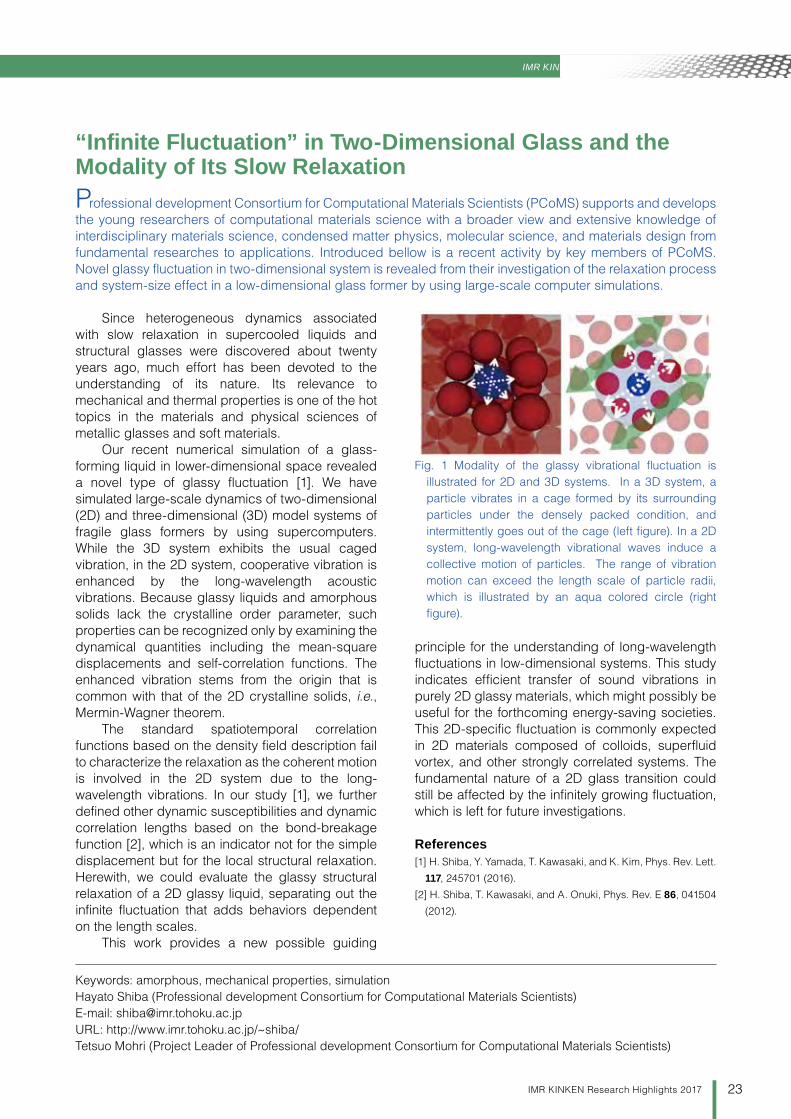
Since heterogeneous dynamics associated with slow relaxation in supercooled liquids and structural glasses were discovered about twenty years ago, much effort has been devoted to the understanding of its nature. Its relevance to mechanical and thermal properties is one of the hot topics in the materials and physical sciences of metallic glasses and soft materials.
Our recent numerical simulation of a glass-forming liquid in lower-dimensional space revealed a novel type of glassy fluctuation [1]. We have simulated large-scale dynamics of two-dimensional (2D) and three-dimensional (3D) model systems of fragile glass formers by using supercomputers. While the 3D system exhibits the usual caged vibration, in the 2D system, cooperative vibration is enhanced by the long-wavelength acoustic vibrations. Because glassy liquids and amorphous solids lack the crystalline order parameter, such properties can be recognized only by examining the dynamical quantities including the mean-square displacements and self-correlation functions. The enhanced vibration stems from the origin that is common with that of the 2D crystalline solids, i.e., Mermin-Wagner theorem.
The standard spatiotemporal correlation functions based on the density field description fail to characterize the relaxation as the coherent motion is involved in the 2D system due to the long-wavelength vibrations. In our study [1], we further defined other dynamic susceptibilities and dynamic correlation lengths based on the bond-breakage function [2], which is an indicator not for the simple displacement but for the local structural relaxation. Herewith, we could evaluate the glassy structural relaxation of a 2D glassy liquid, separating out the infinite fluctuation that adds behaviors dependent on the length scales.
This work provides a new possible guiding
principle for the understanding of long-wavelength fluctuations in low-dimensional systems. This study indicates efficient transfer of sound vibrations in purely 2D glassy materials, which might possibly be useful for the forthcoming energy-saving societies. This 2D-specific fluctuation is commonly expected in 2D materials composed of colloids, superfluid vortex, and other strongly correlated systems. The fundamental nature of a 2D glass transition could still be affected by the infinitely growing fluctuation, which is left for future investigations.
References[1] H. Shiba, Y. Yamada, T. Kawasaki, and K. Kim, Phys. Rev. Lett.
117, 245701 (2016).
[2] H. Shiba, T. Kawasaki, and A. Onuki, Phys. Rev. E 86, 041504
(2012).
“Infinite Fluctuation” in Two-Dimensional Glass and the Modality of Its Slow RelaxationProfessional development Consortium for Computational Materials Scientists (PCoMS) supports and develops the young researchers of computational materials science with a broader view and extensive knowledge of interdisciplinary materials science, condensed matter physics, molecular science, and materials design from fundamental researches to applications. Introduced bellow is a recent activity by key members of PCoMS. Novel glassy fluctuation in two-dimensional system is revealed from their investigation of the relaxation process and system-size effect in a low-dimensional glass former by using large-scale computer simulations.
Keywords: amorphous, mechanical properties, simulationHayato Shiba (Professional development Consortium for Computational Materials Scientists)E-mail: [email protected]: http://www.imr.tohoku.ac.jp/~shiba/Tetsuo Mohri (Project Leader of Professional development Consortium for Computational Materials Scientists)
Fig. 1 Modality of the glassy vibrational fluctuation is illustrated for 2D and 3D systems. In a 3D system, a particle vibrates in a cage formed by its surrounding particles under the densely packed condition, and intermittently goes out of the cage (left figure). In a 2D system, long-wavelength vibrational waves induce a collective motion of particles. The range of vibration motion can exceed the length scale of particle radii, which is illustrated by an aqua colored circle (right figure).


Electronic Materials
IMR KINKEN Research Highlights 2017Research
Electronic Materials
26 IMR KINKEN Research Highlights 2017
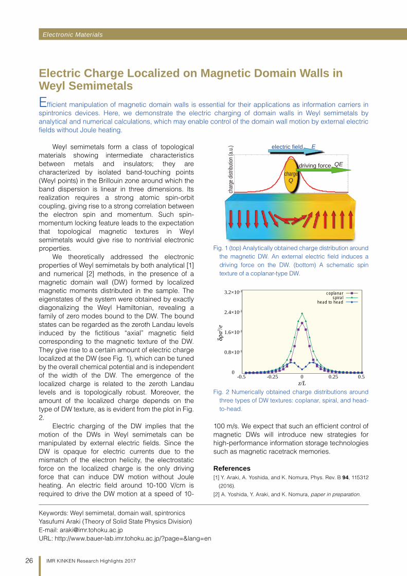
Weyl semimetals form a class of topological materials showing intermediate characteristics between metals and insulators; they are characterized by isolated band-touching points (Weyl points) in the Brillouin zone around which the band dispersion is linear in three dimensions. Its realization requires a strong atomic spin-orbit coupling, giving rise to a strong correlation between the electron spin and momentum. Such spin-momentum locking feature leads to the expectation that topological magnetic textures in Weyl semimetals would give rise to nontrivial electronic properties.
We theoretically addressed the electronic properties of Weyl semimetals by both analytical [1] and numerical [2] methods, in the presence of a magnetic domain wall (DW) formed by localized magnetic moments distributed in the sample. The eigenstates of the system were obtained by exactly diagonalizing the Weyl Hamiltonian, revealing a family of zero modes bound to the DW. The bound states can be regarded as the zeroth Landau levels induced by the fictitious “axial” magnetic field corresponding to the magnetic texture of the DW. They give rise to a certain amount of electric charge localized at the DW (see Fig. 1), which can be tuned by the overall chemical potential and is independent of the width of the DW. The emergence of the localized charge is related to the zeroth Landau levels and is topologically robust. Moreover, the amount of the localized charge depends on the type of DW texture, as is evident from the plot in Fig. 2.
Electric charging of the DW implies that the motion of the DWs in Weyl semimetals can be manipulated by external electric fields. Since the DW is opaque for electric currents due to the mismatch of the electron helicity, the electrostatic force on the localized charge is the only driving force that can induce DW motion without Joule heating. An electric field around 10-100 V/cm is required to drive the DW motion at a speed of 10-
100 m/s. We expect that such an efficient control of magnetic DWs will introduce new strategies for high-performance information storage technologies such as magnetic racetrack memories.
References[1] Y. Araki, A. Yoshida, and K. Nomura, Phys. Rev. B 94, 115312
(2016).
[2] A. Yoshida, Y. Araki, and K. Nomura, paper in preparation.
Electric Charge Localized on Magnetic Domain Walls in Weyl SemimetalsEfficient manipulation of magnetic domain walls is essential for their applications as information carriers in spintronics devices. Here, we demonstrate the electric charging of domain walls in Weyl semimetals by analytical and numerical calculations, which may enable control of the domain wall motion by external electric fields without Joule heating.
Keywords: Weyl semimetal, domain wall, spintronicsYasufumi Araki (Theory of Solid State Physics Division)E-mail: [email protected]: http://www.bauer-lab.imr.tohoku.ac.jp/?page=&lang=en
Fig. 1 (top) Analytically obtained charge distribution around the magnetic DW. An external electric field induces a driving force on the DW. (bottom) A schematic spin texture of a coplanar-type DW.
Fig. 2 Numerically obtained charge distributions around three types of DW textures: coplanar, spiral, and head-to-head.
0.000012
chargedriving force
electric field E
Q
QE
charg
e dist
ributi
on (a
.u.)
-0.5 -0.25 0 0.25 0.5
3.2×10⁻³
2.4×10⁻³
1.6×10⁻³
0.8×10⁻³
0
z/L
δρa3 /e
coplanarspiral
head to head
Electronic Materials IMR KINKEN Research Highlights 2017
27IMR KINKEN Research Highlights 2017
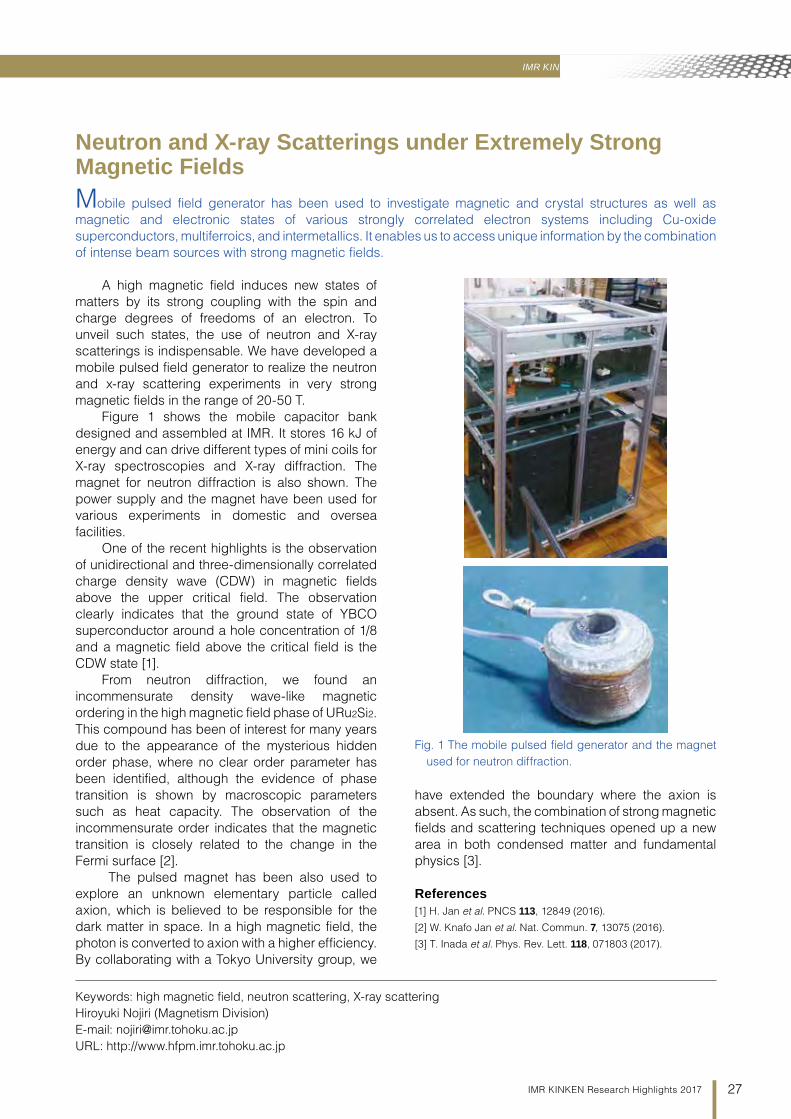
A high magnetic field induces new states of matters by its strong coupling with the spin and charge degrees of freedoms of an electron. To unveil such states, the use of neutron and X-ray scatterings is indispensable. We have developed a mobile pulsed field generator to realize the neutron and x-ray scattering experiments in very strong magnetic fields in the range of 20-50 T.
Figure 1 shows the mobile capacitor bank designed and assembled at IMR. It stores 16 kJ of energy and can drive different types of mini coils for X-ray spectroscopies and X-ray diffraction. The magnet for neutron diffraction is also shown. The power supply and the magnet have been used for various experiments in domestic and oversea facilities.
One of the recent highlights is the observation of unidirectional and three-dimensionally correlated charge density wave (CDW) in magnetic fields above the upper critical field. The observation clearly indicates that the ground state of YBCO superconductor around a hole concentration of 1/8 and a magnetic field above the critical field is the CDW state [1].
From neutron diffraction, we found an incommensurate density wave-like magnetic ordering in the high magnetic field phase of URu2Si2. This compound has been of interest for many years due to the appearance of the mysterious hidden order phase, where no clear order parameter has been identified, although the evidence of phase transition is shown by macroscopic parameters such as heat capacity. The observation of the incommensurate order indicates that the magnetic transition is closely related to the change in the Fermi surface [2].
The pulsed magnet has been also used to explore an unknown elementary particle called axion, which is believed to be responsible for the dark matter in space. In a high magnetic field, the photon is converted to axion with a higher efficiency. By collaborating with a Tokyo University group, we
have extended the boundary where the axion is absent. As such, the combination of strong magnetic fields and scattering techniques opened up a new area in both condensed matter and fundamental physics [3].
References[1] H. Jan et al. PNCS 113, 12849 (2016).
[2] W. Knafo Jan et al. Nat. Commun. 7, 13075 (2016).
[3] T. Inada et al. Phys. Rev. Lett. 118, 071803 (2017).
Neutron and X-ray Scatterings under Extremely Strong Magnetic FieldsMobile pulsed field generator has been used to investigate magnetic and crystal structures as well as magnetic and electronic states of various strongly correlated electron systems including Cu-oxide superconductors, multiferroics, and intermetallics. It enables us to access unique information by the combination of intense beam sources with strong magnetic fields.
Keywords: high magnetic field, neutron scattering, X-ray scattering Hiroyuki Nojiri (Magnetism Division)E-mail: [email protected]: http://www.hfpm.imr.tohoku.ac.jp
Fig. 1 The mobile pulsed field generator and the magnet used for neutron diffraction.
Electronic Materials
28 IMR KINKEN Research Highlights 2017
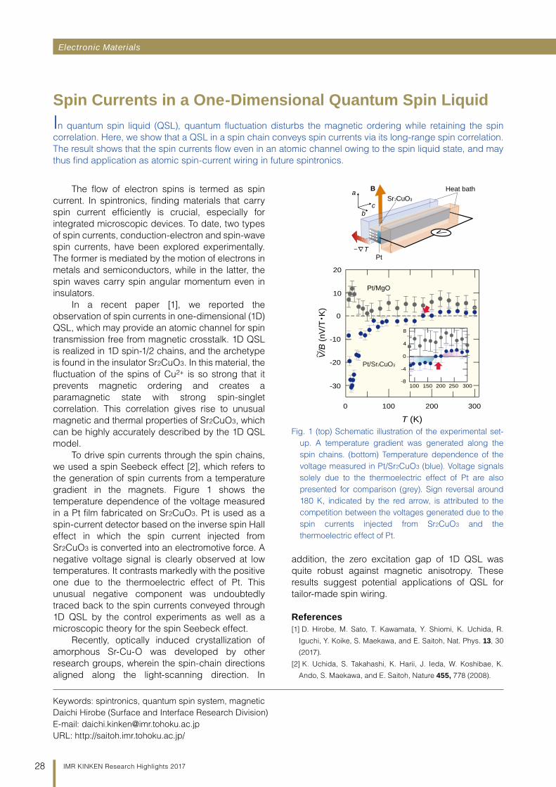
The flow of electron spins is termed as spin current. In spintronics, finding materials that carry spin current efficiently is crucial, especially for integrated microscopic devices. To date, two types of spin currents, conduction-electron and spin-wave spin currents, have been explored experimentally. The former is mediated by the motion of electrons in metals and semiconductors, while in the latter, the spin waves carry spin angular momentum even in insulators.
In a recent paper [1], we reported the observation of spin currents in one-dimensional (1D) QSL, which may provide an atomic channel for spin transmission free from magnetic crosstalk. 1D QSL is realized in 1D spin-1/2 chains, and the archetype is found in the insulator Sr2CuO3. In this material, the fluctuation of the spins of Cu2+ is so strong that it prevents magnetic ordering and creates a paramagnetic state with strong spin-singlet correlation. This correlation gives rise to unusual magnetic and thermal properties of Sr2CuO3, which can be highly accurately described by the 1D QSL model.
To drive spin currents through the spin chains, we used a spin Seebeck effect [2], which refers to the generation of spin currents from a temperature gradient in the magnets. Figure 1 shows the temperature dependence of the voltage measured in a Pt film fabricated on Sr2CuO3. Pt is used as a spin-current detector based on the inverse spin Hall effect in which the spin current injected from Sr2CuO3 is converted into an electromotive force. A negative voltage signal is clearly observed at low temperatures. It contrasts markedly with the positive one due to the thermoelectric effect of Pt. This unusual negative component was undoubtedly traced back to the spin currents conveyed through 1D QSL by the control experiments as well as a microscopic theory for the spin Seebeck effect.
Recently, optically induced crystallization of amorphous Sr-Cu-O was developed by other research groups, wherein the spin-chain directions aligned along the light-scanning direction. In
addition, the zero excitation gap of 1D QSL was quite robust against magnetic anisotropy. These results suggest potential applications of QSL for tailor-made spin wiring.
References[1] D. Hirobe, M. Sato, T. Kawamata, Y. Shiomi, K. Uchida, R.
Iguchi, Y. Koike, S. Maekawa, and E. Saitoh, Nat. Phys. 13, 30
(2017).
[2] K. Uchida, S. Takahashi, K. Harii, J. Ieda, W. Koshibae, K.
Ando, S. Maekawa, and E. Saitoh, Nature 455, 778 (2008).
Spin Currents in a One-Dimensional Quantum Spin LiquidIn quantum spin liquid (QSL), quantum fluctuation disturbs the magnetic ordering while retaining the spin correlation. Here, we show that a QSL in a spin chain conveys spin currents via its long-range spin correlation. The result shows that the spin currents flow even in an atomic channel owing to the spin liquid state, and may thus find application as atomic spin-current wiring in future spintronics.
Keywords: spintronics, quantum spin system, magneticDaichi Hirobe (Surface and Interface Research Division)E-mail: [email protected]: http://saitoh.imr.tohoku.ac.jp/
Fig. 1 (top) Schematic illustration of the experimental set-up. A temperature gradient was generated along the spin chains. (bottom) Temperature dependence of the voltage measured in Pt/Sr2CuO3 (blue). Voltage signals solely due to the thermoelectric effect of Pt are also presented for comparison (grey). Sign reversal around 180 K, indicated by the red arrow, is attributed to the competition between the voltages generated due to the spin currents injected from Sr2CuO3 and the thermoelectric effect of Pt.
T
B
c
a
b
Heat bathSr CuO2 3
Pt
V/B
(nV/
T・K)
~
0 100 200 300
T (K)
20
10
0
-20
-10
-30
Pt/MgO
Pt/Sr CuO2 3
200 250 300150100
8
4
-4
-8
0
Electronic Materials IMR KINKEN Research Highlights 2017
29IMR KINKEN Research Highlights 2017
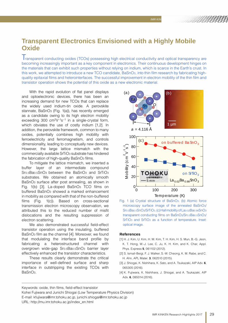
With the rapid evolution of flat panel displays and optoelectronic devices, there has been an increasing demand for new TCOs that can replace the widely used indium-tin oxide. A perovskite stannate, BaSnO3 (Fig. 1(a)), has recently emerged as a candidate owing to its high electron mobility exceeding 300 cm2V−1s−1 in a single-crystal form, which obviates the use of costly indium [1,2]. In addition, the perovskite framework, common to many oxides, potentially combines high mobility with ferroelectricity and ferromagnetism, and controls dimensionality, leading to conceptually new devices. However, the large lattice mismatch with the commercially available SrTiO3 substrate has hindered the fabrication of high-quality BaSnO3 films.
To mitigate the lattice mismatch, we inserted a buffer layer of an intermediate compound Sr0.5Ba0.5SnO3 between the BaSnO3 and SrTiO3 substrates. We obtained an atomically smooth BaSnO3 surface after post annealing, as shown in Fig. 1(b) [3]. La-doped BaSnO3 TCO films on buffered BaSnO3 showed a marked enhancement in mobility as compared with that of the non-buffered films (Fig. 1(c)). Based on cross-sectional transmission electron microscopy observation, we attributed this to the reduced number of misfit dislocations and the resulting suppression of electron scattering.
We also demonstrated successful field-effect transistor operation using the insulating, buffered BaSnO3 film as the channel [4]. Moreover, we found that modulating the interface band profile by fabricating a heterostructured channel with overgrown wide-gap Sr0.5Ba0.5SnO3 barrier layer effectively enhanced the transistor characteristics.
These results clearly demonstrate the critical importance of well-defined surface and sharp interface in outstripping the existing TCOs with BaSnO3.
References[1] H. J. Kim, U. Kim, H. M. Kim, T. H. Kim, H. S. Mun, B.-G. Jeon,
K. T. Hong, W.-J. Lee, C. Ju, K. H. Kim, and K. Char, Appl.
Phys. Express 5, 061102 (2012).
[2] S. Ismail-Beigi, F. J. Walker, S.-W. Cheong, K. M. Rabe, and C.
H. Ahn, APL Mater. 3, 062510 (2015).
[3] J. Shiogai, K. Nishihara, K. Sato, and A. Tsukazaki, AIP Adv. 6,
065305 (2016).
[4] K. Fujiwara, K. Nishihara, J. Shiogai, and A. Tsukazaki, AIP
Adv. 6, 085014 (2016).
Transparent Electronics Envisioned with a Highly Mobile OxideTransparent conducting oxides (TCOs) possessing high electrical conductivity and optical transparency are becoming increasingly important as a key component in electronics. Their continuous development hinges on the materials that can exhibit such properties without relying on indium, which is scarce in the Earth’s crust. In this work, we attempted to introduce a new TCO candidate, BaSnO3, into thin film research by fabricating high-quality epitaxial films and heterointerfaces. The successful improvement in electron mobility of the thin film and transistor operation shows the potential of this oxide as a new electronic material.
Keywords: oxide, thin films, field-effect transistorKohei Fujiwara and Junichi Shiogai (Low Temperature Physics Division)E-mail: [email protected], [email protected]: http://mu.imr.tohoku.ac.jp/index_en.html
Fig. 1 (a) Crystal structure of BaSnO3. (b) Atomic force microscopy surface image of the annealed BaSnO3/Sr0.5Ba0.5SnO3/SrTiO3. (c) Hall mobility of La0.02Ba0.98SnO3 transparent conducting films on BaSnO3/Sr0.5Ba0.5SnO3/SrTiO3 and SrTiO3 as a function of temperature. Inset: optical image.
1 µm
Ba
Sn O
a = 4.116 Å
(a)
(c)
(b)
100
80
60
40
20
0
Mob
ility
(cm
2 V-1
s-1)
3002001000Temperature (K)
on buffered BaSnO3
on SrTiO3
La0.02Ba0.98SnO35 mm
Electronic Materials
30 IMR KINKEN Research Highlights 2017
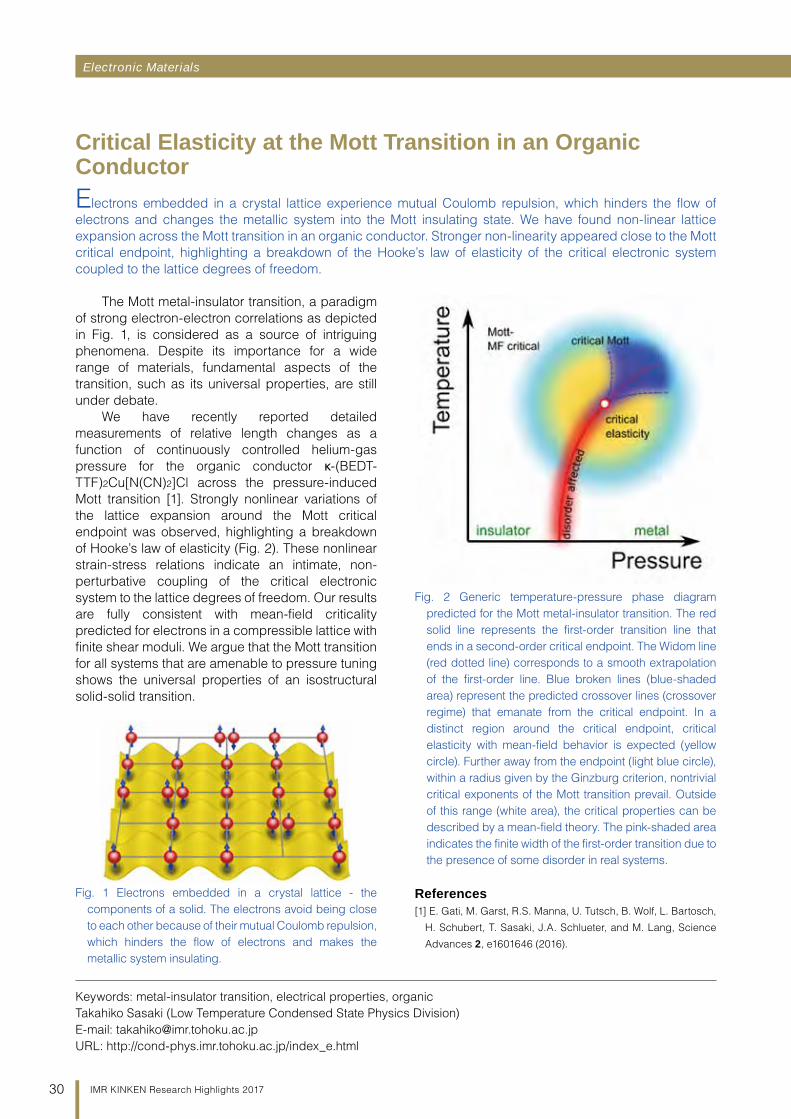
The Mott metal-insulator transition, a paradigm of strong electron-electron correlations as depicted in Fig. 1, is considered as a source of intriguing phenomena. Despite its importance for a wide range of materials, fundamental aspects of the transition, such as its universal properties, are still under debate.
We have recently reported detailed measurements of relative length changes as a function of continuously controlled helium-gas pressure for the organic conductor κ-(BEDT-TTF)2Cu[N(CN)2]Cl across the pressure-induced Mott transition [1]. Strongly nonlinear variations of the lattice expansion around the Mott critical endpoint was observed, highlighting a breakdown of Hooke’s law of elasticity (Fig. 2). These nonlinear strain-stress relations indicate an intimate, non-perturbative coupling of the critical electronic system to the lattice degrees of freedom. Our results are fully consistent with mean-field criticality predicted for electrons in a compressible lattice with finite shear moduli. We argue that the Mott transition for all systems that are amenable to pressure tuning shows the universal properties of an isostructural solid-solid transition.
References[1] E. Gati, M. Garst, R.S. Manna, U. Tutsch, B. Wolf, L. Bartosch,
H. Schubert, T. Sasaki, J.A. Schlueter, and M. Lang, Science
Advances 2, e1601646 (2016).
Critical Elasticity at the Mott Transition in an Organic ConductorElectrons embedded in a crystal lattice experience mutual Coulomb repulsion, which hinders the flow of electrons and changes the metallic system into the Mott insulating state. We have found non-linear lattice expansion across the Mott transition in an organic conductor. Stronger non-linearity appeared close to the Mott critical endpoint, highlighting a breakdown of the Hooke’s law of elasticity of the critical electronic system coupled to the lattice degrees of freedom.
Keywords: metal-insulator transition, electrical properties, organicTakahiko Sasaki (Low Temperature Condensed State Physics Division)E-mail: [email protected]: http://cond-phys.imr.tohoku.ac.jp/index_e.html
Fig. 1 Electrons embedded in a crystal lattice - the components of a solid. The electrons avoid being close to each other because of their mutual Coulomb repulsion, which hinders the flow of electrons and makes the metallic system insulating.
Fig. 2 Generic temperature-pressure phase diagram predicted for the Mott metal-insulator transition. The red solid line represents the first-order transition line that ends in a second-order critical endpoint. The Widom line (red dotted line) corresponds to a smooth extrapolation of the first-order line. Blue broken lines (blue-shaded area) represent the predicted crossover lines (crossover regime) that emanate from the critical endpoint. In a distinct region around the critical endpoint, critical elasticity with mean-field behavior is expected (yellow circle). Further away from the endpoint (light blue circle), within a radius given by the Ginzburg criterion, nontrivial critical exponents of the Mott transition prevail. Outside of this range (white area), the critical properties can be described by a mean-field theory. The pink-shaded area indicates the finite width of the first-order transition due to the presence of some disorder in real systems.
Electronic Materials IMR KINKEN Research Highlights 2017
31IMR KINKEN Research Highlights 2017
In heavy fermion physics, the effects of the lack of parity symmetry in crystals, as well as the magnetic quantum critical phenomena have at-tracted much interest as a key to understanding the anomalous superconducting behaviors observed in CeTSi3 systems (T = transition metal) [1]. In noncentrosymmetric (NCS) systems, a finite antisymmetric spin-orbit coupling allows the admixture of spin-singlet and spin-triplet superconducting state and possibly brings about novel superconducting and magnetic behaviors. Nevertheless, it seems that parity symmetry breaking (PSB) is not a necessary and sufficient condition for the emergence of anomalous superconductivity and magnetism. In this context, as is evident from the comparison between Ce(4f 1) and La(4f 0) compounds, 4f electrons probably play a crucial role in the anomalous behaviors observed in those systems.
For conventional NCS insulating magnets, the magnetic properties can be described with a simple effective Hamiltonian modified by a DM type interaction. On the other hand, in an NCS heavy fermion system, the RKKY type long-range interaction and the Kondo effect will render the magnetic properties more complicated and di-verse. Even when we focus only on magnetism, our understanding of the effects of PSB in 4f electron systems is still lacking. Here, we examine such PSB effects in the NCS CePdSi3. In this compound, the 4f electrons are rather localized [1] compared with those of the other Ce-TSi3 systems, such that it may be easier to understand the PSB effects on the 4f-electron magnetism.
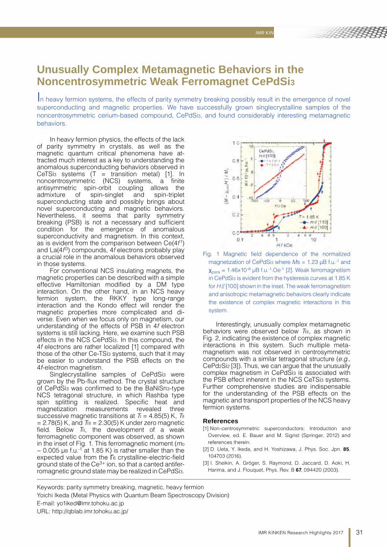
Singlecrystalline samples of CePdSi3 were grown by the Pb-flux method. The crystal structure of CePdSi3 was confirmed to be the BaNiSn3-type NCS tetragonal structure, in which Rashba type spin splitting is realized. Specific heat and magnetization measurements revealed three successive magnetic transitions at TI = 4.85(5) K, TII = 2.78(5) K, and TIII = 2.30(5) K under zero magnetic field. Below TII, the development of a weak ferromagnetic component was observed, as shown in the inset of Fig. 1. This ferromagnetic moment (mo ~ 0.005 μB f.u.-1 at 1.85 K) is rather smaller than the expected value from the Γ6 crystalline-electric-field ground state of the Ce3+ ion, so that a canted antifer-romagnetic ground state may be realized in CePdSi3.
Interestingly, unusually complex metamagnetic behaviors were observed below TIII, as shown in Fig. 2, indicating the existence of complex magnetic interactions in this system. Such multiple meta-magnetism was not observed in centrosymmetric compounds with a similar tetragonal structure (e.g., CePd2Si2 [3]). Thus, we can argue that the unusually complex magnetism in CePdSi3 is associated with the PSB effect inherent in the NCS CeTSi3 systems. Further comprehensive studies are indispensable for the understanding of the PSB effects on the magnetic and transport properties of the NCS heavy fermion systems.
References[1] Non-centrosymmetric superconductors: Introduction and
Overview, ed. E. Bauer and M. Sigrist (Springer, 2012) and references therein.
[2] D. Ueta, Y. Ikeda, and H. Yoshizawa, J. Phys. Soc. Jpn. 85, 104703 (2016).
[3] I. Sheikin, A. Gröger, S. Raymond, D. Jaccard, D. Aoki, H. Harima, and J. Flouquet, Phys. Rev. B 67, 094420 (2003).
Unusually Complex Metamagnetic Behaviors in the Noncentrosymmetric Weak Ferromagnet CePdSi3In heavy fermion systems, the effects of parity symmetry breaking possibly result in the emergence of novel superconducting and magnetic properties. We have successfully grown singlecrystalline samples of the noncentrosymmetric cerium-based compound, CePdSi3, and found considerably interesting metamagnetic behaviors.
Keywords: parity symmetry breaking, magnetic, heavy fermionYoichi Ikeda (Metal Physics with Quantum Beam Spectroscopy Division)E-mail: [email protected]: http://qblab.imr.tohoku.ac.jp/
Fig. 1 Magnetic field dependence of the normalized magnetization of CePdSi3 where Ms = 1.23 μB f.u.-1 and χpara = 1.46x10⁻⁶ μB f.u.-1.Oe-1 [2]. Weak ferromagnetism in CePdSi3 is evident from the hysteresis curves at 1.85 K for H // [100] shown in the inset. The weak ferromagnetism and anisotropic metamagnetic behaviors clearly indicate the existence of complex magnetic interactions in this system.
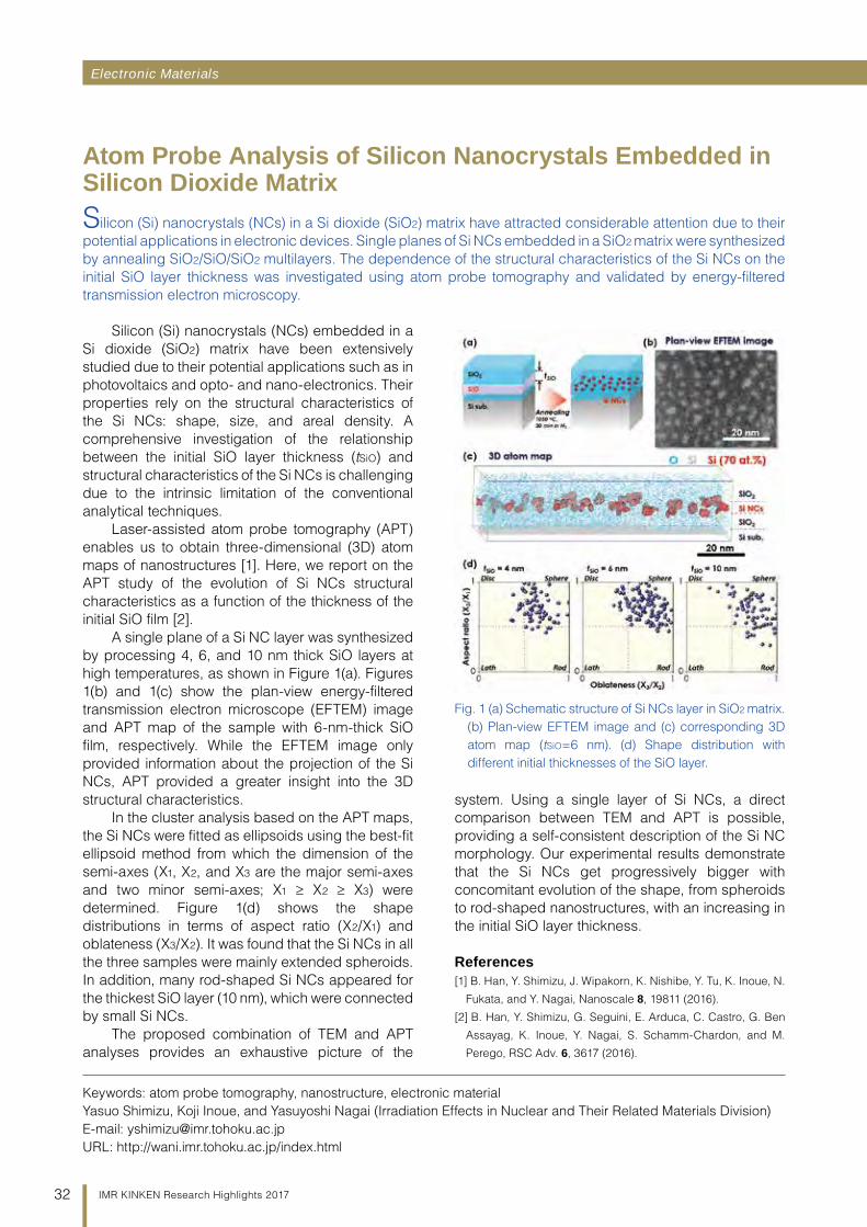
Electronic Materials
32 IMR KINKEN Research Highlights 2017
Silicon (Si) nanocrystals (NCs) embedded in a Si dioxide (SiO2) matrix have been extensively studied due to their potential applications such as in photovoltaics and opto- and nano-electronics. Their properties rely on the structural characteristics of the Si NCs: shape, size, and areal density. A comprehensive investigation of the relationship between the initial SiO layer thickness (tSiO) and structural characteristics of the Si NCs is challenging due to the intrinsic limitation of the conventional analytical techniques.
Laser-assisted atom probe tomography (APT) enables us to obtain three-dimensional (3D) atom maps of nanostructures [1]. Here, we report on the APT study of the evolution of Si NCs structural characteristics as a function of the thickness of the initial SiO film [2].
A single plane of a Si NC layer was synthesized by processing 4, 6, and 10 nm thick SiO layers at high temperatures, as shown in Figure 1(a). Figures 1(b) and 1(c) show the plan-view energy-filtered transmission electron microscope (EFTEM) image and APT map of the sample with 6-nm-thick SiO film, respectively. While the EFTEM image only provided information about the projection of the Si NCs, APT provided a greater insight into the 3D structural characteristics.
In the cluster analysis based on the APT maps, the Si NCs were fitted as ellipsoids using the best-fit ellipsoid method from which the dimension of the semi-axes (X1, X2, and X3 are the major semi-axes and two minor semi-axes; X1 ≥ X2 ≥ X3) were determined. Figure 1(d) shows the shape distributions in terms of aspect ratio (X2/X1) and oblateness (X3/X2). It was found that the Si NCs in all the three samples were mainly extended spheroids. In addition, many rod-shaped Si NCs appeared for the thickest SiO layer (10 nm), which were connected by small Si NCs.
The proposed combination of TEM and APT analyses provides an exhaustive picture of the
system. Using a single layer of Si NCs, a direct comparison between TEM and APT is possible, providing a self-consistent description of the Si NC morphology. Our experimental results demonstrate that the Si NCs get progressively bigger with concomitant evolution of the shape, from spheroids to rod-shaped nanostructures, with an increasing in the initial SiO layer thickness.
References[1] B. Han, Y. Shimizu, J. Wipakorn, K. Nishibe, Y. Tu, K. Inoue, N.
Fukata, and Y. Nagai, Nanoscale 8, 19811 (2016).
[2] B. Han, Y. Shimizu, G. Seguini, E. Arduca, C. Castro, G. Ben
Assayag, K. Inoue, Y. Nagai, S. Schamm-Chardon, and M.
Perego, RSC Adv. 6, 3617 (2016).
Atom Probe Analysis of Silicon Nanocrystals Embedded in Silicon Dioxide MatrixSilicon (Si) nanocrystals (NCs) in a Si dioxide (SiO2) matrix have attracted considerable attention due to their potential applications in electronic devices. Single planes of Si NCs embedded in a SiO2 matrix were synthesized by annealing SiO2/SiO/SiO2 multilayers. The dependence of the structural characteristics of the Si NCs on the initial SiO layer thickness was investigated using atom probe tomography and validated by energy-filtered transmission electron microscopy.
Keywords: atom probe tomography, nanostructure, electronic materialYasuo Shimizu, Koji Inoue, and Yasuyoshi Nagai (Irradiation Effects in Nuclear and Their Related Materials Division)E-mail: [email protected]: http://wani.imr.tohoku.ac.jp/index.html
Fig. 1 (a) Schematic structure of Si NCs layer in SiO2 matrix. (b) Plan-view EFTEM image and (c) corresponding 3D atom map (tSiO=6 nm). (d) Shape distribution with different initial thicknesses of the SiO layer.
Electronic Materials IMR KINKEN Research Highlights 2017
33IMR KINKEN Research Highlights 2017
In order to realize a sustainable society, further improvement of nitride-based devices, including light emitters and optical detectors, high-power and high-frequency transistors, and high-efficiency tandem solar cells is indispensable. To date, sapphire substrates with a large lattice mismatch of 14% to GaN have been usually used. This context shows that, ScAlMgO4 (SCAM) with a small lattice mismatch of 1.8% to GaN is attractive. A two-inch-size boule of SCAM can be grown by the Czochralski method. Moreover, SCAM can be cleaved along the c-plane as illustrated in Fig. 1(a). We have confirmed the cleavage position by using the X-ray crystal truncation rod scattering method. Thus, atomically flat c-plane substrates with large diameters can be easily prepared just by cleavage without slicing by a cutter and polishing. This leads to the drastic cost reduction in substrate fabrication.
The successful growth of flat and high-quality GaN films by metalorganic vapor phase epitaxy (MOVPE) indicates that the SCAM substrate is resistant to the MOVPE environment [1]. The film was proven to be (0001) Ga-polar due to the discrimination of etching with a KOH aqueous solution, as illustrated in Fig. 1(b). This result was carefully verified by anomalous scattering X-ray diffraction measurements using a continuous-energy X-ray. The residual strain of a 2-µm-thick film was characterized by the reciprocal space mapping of X-ray diffraction as shown in Fig. 2. The c- and a-axis lattice constants of GaN were measured to be 5.187 and 3.187 Å, respectively. From these results, the strains are 0.029% and -0.055% along the c-axis and a-axis, respectively. These strains are almost half of the strains in a Ga-polar GaN film grown on a sapphire substrate [2]. Hence, SCAM is a very promising substrate material for nitride semiconductors grown using MOVPE.
SCAM is also expected to be a potential substrate for bulk GaN fabrication via the halide vapor phase epitaxy (HVPE) growth method owing to its small residual strain, small bowing, and the feasibility of substrate removal by cleavage.
References[1] T. Iwabuchi, S. Kuboya, T. Tanikawa, T. Hanada, R. Katayama,
T. Fukuda, and T. Matsuoka, Phys. Status Solidi A, 1-8, DOI:
10.1002/pssa.201600754 (2016).
[2] K. Shojiki, T. Hanada, T. Tanikawa, Y. Imai, S. Kimura, R.
Nonoda, S. Kuboya, R. Katayama, and T. Matsuoka, Jpn. J.
Appl. Phys. 55, 05FA09 (2016).
Cleaved ScAlMgO4 (0001) as a Suitable Substrate for GaN Epitaxial Growth by Metalorganic Vapor Phase EpitaxyCleaved ScAlMgO4 (SCAM) substrates with small lattice mismatch of 1.8% to GaN were used for metalorganic vapor phase epitaxial growth of GaN. A single crystalline GaN film with a flat surface and a small residual strain was obtained. These results reveal that the cleaved SCAM substrate is very promising for nitride semiconductors.
Keywords: nitride, thin films, vapor phase epitaxy (VPE)Takashi Matsuoka (Physics of Electronic Materials Division)E-mail: [email protected]: http://www.matsuoka-lab.imr.tohoku.ac.jp/?TOPPAGE_ENG
Fig. 1 Cross-sectional atomic structure of (a) SCAM and cleavage planes, and (b) an interface model of Ga-polar GaN grown on a cleaved SCAM substrate.
Fig. 2 Reciprocal space map around SCAM (01123) and GaN (0115). The void center of the white cross indicates the point for bulk GaN.
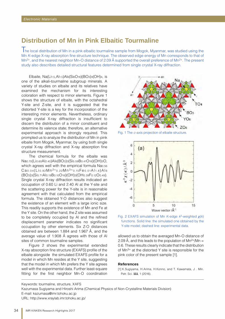
Electronic Materials
34 IMR KINKEN Research Highlights 2017
Elbaite, Na(Li1.5,Al1.5)Al6(Si6O18)(BO3)3(OH)4, is one of the alkali-tourmaline subgroup minerals. A variety of studies on elbaite and its relatives have examined the mechanism for its interesting coloration with respect to minor elements. Figure 1 shows the structure of elbaite, with the octahedral Y-site and Z-site, and it is suggested that the distorted Y-site is a key for the incorporation of the interesting minor elements. Nevertheless, ordinary single crystal X-ray diffraction is insufficient to discern the distribution of a minor constituent and determine its valence state; therefore, an alternative experimental approach is strongly required. This prompted us to analyze the distribution of Mn in pink elbaite from Mogok, Myanmar, by using both single crystal X-ray diffraction and X-ray absorption fine structure measurement.
The chemical formula for the elbaite was Na0.70(Li0.60Al2.40)Al6(BO3)3(Si5.59B0.41O18)(OH)3O, which agrees well with the empirical formula Na0.56
Ca 0.0 4 (L i 0 . 8 2Mn 2+ 0 . 2 2Mn 3 + 0 .15Fe 0.01A l1. 8)A l 6
(BO3)3(Si5.71Al0.19B0.10O18)(OH)3(OH0.39F0.12O0.49). Single crystal X-ray diffraction results indicated an occupation of 0.60 Li and 2.40 Al at the Y-site and the scattering power for the Y-site is in reasonable agreement with that calculated from the empirical formula. The obtained Y-O distances also suggest the existence of an element with a large ionic size. This readily supports the existence of Mn and Fe at the Y site. On the other hand, the Z site was assumed to be completely occupied by Al and the refined displacement parameter indicates no significant occupation by other elements. Six Z-O distances obtained are between 1.884 and 1.967 Å, and the average value of 1.908 Å agrees with those of Al sites of common tourmaline samples.
Figure 2 shows the experimental extended X-ray absorption fine structure (EXAFS) profile of the elbaite alongside the simulated EXAFS profile for a model in which Mn resides at the Y site, suggesting that the model in which Mn prefers the Y site agrees well with the experimental data. Further least-square fitting for the first neighbor Mn-O coordination
allowed us to obtain the averaged Mn-O distance of 2.09 Å, and this leads to the population of Mn2+/Mn = 0.6. These results clearly indicate that the distribution of Mn3+ at the distorted Y site is responsible for the pink color of the present sample [1].
References[1] K.Sugiyama, H.Arima, H.Konno, and T. Kawamata, J . Min.
Petr. Sci. 111, 1 (2016).
Distribution of Mn in Pink Elbaitic TourmalineThe local distribution of Mn in a pink elbaitic tourmaline sample from Mogok, Myanmar, was studied using the Mn K-edge X-ray absorption fine structure technique. The observed edge energy of Mn corresponds to that of Mn2+, and the nearest neighbor Mn-O distance of 2.09 Å supported the overall preference of Mn2+. The present study also describes detailed structural features determined from single crystal X-ray diffraction.
Keywords: tourmaline, structure, XAFSKazumasa Sugiyama and Hiroshi Arima (Chemical Physics of Non-Crystalline Materials Division)E-mail: [email protected]: http://www.xraylab.imr.tohoku.ac.jp/
Fig. 1 The c-axis projection of elbaite structure.
Fig. 2 EXAFS simulation of Mn K-edge k3-weighted χ(k) functions. Solid line: the simulated one obtained by the Y-site model; dashed line: experimental data.
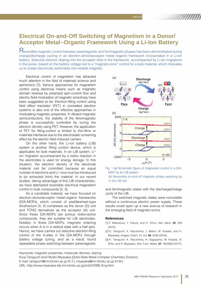
Electronic Materials IMR KINKEN Research Highlights 2017
35IMR KINKEN Research Highlights 2017
Electrical control of magnetism has attracted much attention in the field of materials science and spintronics [1]. Various approaches for magnetism control using electrical means such as magnetic domain reversal by polarized spin-current flow and electric-field modulation of magnetic anisotropy have been suggested so far. Electron-filling control using field effect transistor (FET) in correlated electron systems is also one of the effective approaches in modulating magnetic properties. In diluted magnetic semiconductors, the stability of the ferromagnetic phase is successfully controlled by tuning the electron density using FET. However, the application of FET for filling-control is limited to thin-films or materials interfaces due to the electrostatic screening effect by the electric-field-induced carriers.
On the other hand, the Li-ion battery (LIB) system is another filling control device, which is applicable for bulk materials. In an LIB system, Li+ ion migration accompanied by a redox reaction in the electrodes is used for energy storage. In this situation, the electron density of the electrode material can be controlled because an equal number of electrons and Li+ ions must be introduced to (or extracted from) the material. In our recent studies, taking advantage of this LIB characteristic, we have attempted reversible electrical magnetism control in bulk compounds [2, 3].
As a candidate material, we have focused on electron-donor/acceptor metal-organic frameworks (D/A-MOFs), which consist of paddlewheel-type diruthenium (II, II) complexes as the donor (D) unit and TCNQ derivatives as the acceptor (A) unit. Since these D/A-MOFs are porous redox-active compounds, they are suitable for LIB electrodes. Notably, in these D/A-MOFs, magnetic ordering occurs when A is in a radical state with a half spin. Hence, we have carried out selective electron-filing control of the A-sites in the D/A-MOFs through battery voltage tuning, and as a result, found repeatable phase switching between paramagnetic
and ferrimagnetic states with the discharge/charge cycle of the LIB.
The switched magnetic states were nonvolatile without a continuous electric power supply. These results could open up a new avenue of research in the emerging field of magneto-ionics.
References[1] F. Matsukura, Y. Tokura, and H. Ohno, Nat. Nano. 10, 209
(2015).
[2] K. Taniguchi, K. Narushima, J. Mahin, W. Kosaka, and H.
Miyasaka, Angew. Chem. Int. Ed. 55, 5238 (2016).
[3] K. Taniguchi, K. Narushima, H. Sagayama, W. Kosaka, N.
Shito, and H. Miyasaka, Adv. Func. Mater. 27, 1604990 (2017).
Electrical On-and-Off Switching of Magnetism in a Donor/Acceptor Metal–Organic Framework Using a Li-Ion BatteryReversible magnetic control between paramagnetic and ferrimagnetic phases has been demonstrated during charge/discharge cycling in an electron-donor/acceptor metal–organic framework incorporated in a Li-ion battery. Selective electron doping into the acceptor sites in the framework, accompanied by Li-ion migrations in the pores, based on the battery voltage led to a “magneto-ionic” control for a bulk material, which motivates us to create electrically switchable non-volatile magnets.
Keywords: magnetic properties, molecular devices, dopingKouji Taniguchi and Hitoshi Miyasaka (Solid-State Metal-Complex Chemistry Division)E-mail: [email protected] (K.T.), [email protected] (H.M.)URL: http://www.miyasaka-lab.imr.tohoku.ac.jp/cn5/HOME-Eng.html
Fig. 1 (a) Schematic figure of magnetism control in a D/A-MOF by an LIB system. (b) Reversible on-and-off magnetic phase switching by in situ LIB cell.
Electronic Materials
36 IMR KINKEN Research Highlights 2017
A magnetic vortex in a soft magnetic disk is an in-plane curling magnetic structure having a core whose magnetic moments are normal to the disk plane. Magnetic vortices have fascinated us because of their unique functionalities and rich physics [1]. Several kinds of non-equilibrium dynamical motion can be excited by applying an rf magnetic field (Hrf) or injecting spin current, which provide promising applications, e.g., a vortex-type magnetic random access memory and a spin torque vortex oscillator. Although many studies related to a magnetic vortex focus on the control of magnetic moments in the vortex [2], none has tried to use the magnetic vortex dynamics in a soft magnet as a route to switching the magnetization of a hard magnet. Here, we show that the Hrf-induced vortex dynamics in soft magnetic Ni81Fe19 (permalloy; Py) trigger the magnetization switching of hard magnetic L10-FePt at a low magnetic field (H) [3].
We exploited a nanodot array consisting of an exchange-coupled bilayer with a hard magnetic L10-FePt layer and a soft magnetic Py layer, which is schematically illustrated in Fig. 1 (a). The thin films were grown on an MgO (100) single crystal substrate in the stacking order of MgO Subs. || Fe (1) | Au (60) | L10-FePt (10) | Py (150) | Au (5) | Pt (3) (in nanometers) by sputtering. The films were microfabricated into circular nanodots with a diameter of 260 nm by electron beam lithography and Ar ion milling. The 10-nm-thick L10-FePt had large uniaxial magnetocrystalline anisotropy (Ku) perpendicular to the disk plane, leading to perpendicular magnetization. On the other hand, micromagnetic simulation suggested the formation of magnetic vortex in the 150-nm-thick Py layer.
From the magnetization curve and the anisotropic magnetoresistance curve for the nanodot array, we recorded a large Hsw of 8.6 kOe for L10-FePt without exciting the dynamics of the magnetic vortex. In order to examine the effect of vortex dynamics on Hsw, we applied Hrf of 200 Oe to the nanodots to excite the vortex dynamics in Py. Figure 1 (b) shows a plot of Hsw as a function of
frequency (f) of Hrf. Compared to Hsw with no applied Hrf, a strong reduction of Hsw is evident in the range of 11 GHz ≤ f ≤ 17 GHz. In this f range, Hsw gradually increases, and the values of Hsw in f ≥ 18 GHz are almost the same as those in 6 GHz ≤ f ≤ 10 GHz. Micromagnetic simulation and the detailed analysis of the magnetization reversal process revealed that the azimuthal spin waves having node in the radial direction in Py played an important role for the reversed-domain nucleation in L10-FePt. Consequently, we achieved a reduction in Hsw for L10-FePt. This is regarded as a nonlocal phenomenon in a coupled system.
Our results not only provide an insight into the nucleation phenomena but also offer a new way for information writing of magnetic storage, and spintronic applications.
References[1] S.-B. Choe, Y. Acremann, A. Scholl, A. Bauer, A. Doran, J.
Stöhr, and H. A. Padmore, Science 304, 420 (2004).
[2] B. Van Waeyenberge, A. Puzic, H. Stoll, K. W. Chou, T.
Tyliszczak, R. Hertel, M. Fähnle, H. Brückl, K. Rott, G. Reiss, I.
Neudecker, D. Weiss, C. H. Back, and G. Schütz, Nature 444,
461 (2006).
[3] W. Zhou, T. Seki, H. Arai, H. Imamura, and K. Takanashi, Phys.
Rev. B 94, 220401(R) (2016).
Low Field Magnetization Switching Mediated by Vortex DynamicsMagnetic vortex dynamics strongly affects the magnetic structures of environment. We fabricated nanodots of an exchange-coupled bilayer with a soft magnetic Ni81Fe19 having a magnetic vortex and a perpendicularly magnetized L10-FePt exhibiting a large switching field. The azimuthal spin waves in the magnetic vortex of Ni81Fe19 triggered the reversed-domain nucleation in L10-FePt, which led to low field magnetization switching.
Keywords: magnetic properties, spin dynamicsKoki Takanashi (Magnetic Materials Division)E-mail: [email protected]://magmatelab.imr.tohoku.ac.jp/
Fig. 1 (a) Schematic illustration of nanodots consisting of perpendicularly magnetized L10-FePt, and Py having the magnetic vortex. (b) Switching field (Hsw) as a function of frequency (f) of an rf magnetic field.
10
8
6
4
2
0
H s
w (k
Oe)
2520151050f (GHz)
Experiment Simulation
FePt
Py
a b
Electronic Materials IMR KINKEN Research Highlights 2017
37IMR KINKEN Research Highlights 2017
Atomic and electronic properties of l-Si are largely different from those of a-Si: l-Si is metallic and its coordination number is about 6, whereas a-Si is semiconducting and its coordination number is 4. The transformation from l-Si to a-Si could be a first-order phase transition, which releases latent heat. Therefore, obtaining “bulk” a-Si directly from the melt is extremely challenging. Recently, Turnbull et al. have proposed that a-Si can be obtained from supercooled states below 1440 K [1].
However, it is difficult to cool liquids to several hundred K below the melting temperature (Tm: 1683 K) because liquids are generally held in containers or crucibles. When the temperatures of liquids decrease below Tm, heterogeneous nucleation at the wall of the container occurs and crystallization starts; thus, the temperature of liquid does not decrease below Tm.
We have developed a unique liquid-quenching system including an electrostatic levitator (ESL). In the ESL system, a sample is levitated between two horizontal electrodes using electrostatic forces via a feedback loop (Fig. 1). The sample is heated and melted using the focused beams of three 100 semiconductor lasers at a wavelength of 980 nm. The radiance temperature is measured by pyrometry at the wavelength of 2.4 μm. A feature of our system is to hold the sample via Coulomb forces instead of using a crucible (i.e., the sample is free from the container walls) throughout the processing. This way, we can achieve and maintain the supercooled states of l-Si.
Our experimental procedure was as follows. The high-purity polycrystalline Si sample was melted and kept in the molten state at 1883 K for several seconds. Then, turning off the heating laser beams, the l-Si droplet was cooled by radiation from the surface. When the temperature of the droplet decreased to that of supercooled states, the high voltage used for levitating the droplet was switched off, and it fell through a hole in the bottom electrode. The falling droplet came in contact with a metal plate and quenched. The thickness of the quenched sample was 10–200 µm.
Though the X-ray diffraction pattern pattern of the quenched sample showed only the diffraction
peaks of crystalline Si, a characteristic microstructure was observed locally in the quenched sample (Fig. 2). The microstructure was composed of Si grains with a diameter of several tens of nm. The microstructure indicates that a-Si can locally form once during the quenching process and then transforms to crystalline Si grains by the latent heat from the surroundings. We hope to obtain bulk a-Si by further improving the quenching method.
References[1] Y. Shao, F. Spaepen, and D. Turnbull, Metall. Mat. Trans A 29,
1825 (1998).
Challenge to Produce Amorphous-Si from Supercooled LiquidAmorphous silicon (a-Si) is mainly used in solid-state electronics and photovoltaic technologies, and is usually produced as thin films by chemical vapor deposition. The preparation of bulk a-Si from liquid (l-) Si has long been a challenge since all attempts have failed so far. The purpose of this study is, therefore, to produce bulk a-Si directly from l-Si.
Keywords: amorphous, Si, supercooled liquidJunpei Okada and Satoshi Uda (Crystal Chemistry Division)E-mail: [email protected]: http://www.uda-lab.imr.tohoku.ac.jp/ index.html
Fig. 1 Interior of the ESL chamber: A spherical sample is levitated between two horizontal electrodes using electrostatic forces. The bottom electrode is electrically grounded. An electrical field of about 10 kV is applied to the top electrode to levitate the sample against gravity.
Fig. 2 An scanning electron microscope image of the quenched sample from supercooled l-Si.
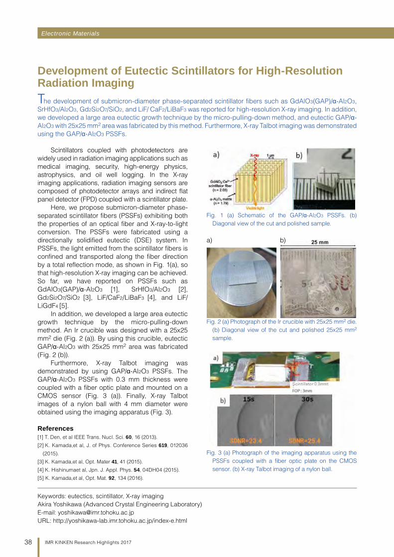
Electronic Materials
38 IMR KINKEN Research Highlights 2017
Scintillators coupled with photodetectors are widely used in radiation imaging applications such as medical imaging, security, high-energy physics, astrophysics, and oil well logging. In the X-ray imaging applications, radiation imaging sensors are composed of photodetector arrays and indirect flat panel detector (FPD) coupled with a scintillator plate.
Here, we propose submicron-diameter phase-separated scintillator fibers (PSSFs) exhibiting both the properties of an optical fiber and X-ray-to-light conversion. The PSSFs were fabricated using a directionally solidified eutectic (DSE) system. In PSSFs, the light emitted from the scintillator fibers is confined and transported along the fiber direction by a total reflection mode, as shown in Fig. 1(a), so that high-resolution X-ray imaging can be achieved. So far, we have reported on PSSFs such as GdAlO3(GAP)/α-Al2O3 [1], SrHfO3/Al2O3 [2], Gd2Si2O7/SiO2 [3], LiF/CaF2/LiBaF3 [4], and LiF/LiGdF4 [5].
In addition, we developed a large area eutectic growth technique by the micro-pulling-down method. An Ir crucible was designed with a 25x25 mm2 die (Fig. 2 (a)). By using this crucible, eutectic GAP/α-Al2O3 with 25x25 mm2 area was fabricated (Fig. 2 (b)).
Furthermore, X-ray Talbot imaging was demonstrated by using GAP/α-Al2O3 PSSFs. The GAP/α-Al2O3 PSSFs with 0.3 mm thickness were coupled with a fiber optic plate and mounted on a CMOS sensor (Fig. 3 (a)). Finally, X-ray Talbot images of a nylon ball with 4 mm diameter were obtained using the imaging apparatus (Fig. 3).
References[1] T. Den, et al IEEE Trans. Nucl. Sci. 60, 16 (2013).
[2] K. Kamada,et al, J. of Phys. Conference Series 619, 012036
(2015).
[3] K. Kamada,et al, Opt. Mater 41, 41 (2015).
[4] K. Hishinumaet al, Jpn. J. Appl. Phys. 54, 04DH04 (2015).
[5] K. Kamada,et al, Opt. Mat. 92, 134 (2016).
Development of Eutectic Scintillators for High-Resolution Radiation ImagingThe development of submicron-diameter phase-separated scintillator fibers such as GdAlO3(GAP)/α-Al2O3, SrHfO3/Al2O3, Gd2Si2O7/SiO2, and LiF/ CaF2/LiBaF3 was reported for high-resolution X-ray imaging. In addition, we developed a large area eutectic growth technique by the micro-pulling-down method, and eutectic GAP/α-Al2O3 with 25x25 mm2 area was fabricated by this method. Furthermore, X-ray Talbot imaging was demonstrated using the GAP/α-Al2O3 PSSFs.
Keywords: eutectics, scintillator, X-ray imagingAkira Yoshikawa (Advanced Crystal Engineering Laboratory)E-mail: [email protected]: http://yoshikawa-lab.imr.tohoku.ac.jp/index-e.html
Fig. 1 (a) Schematic of the GAP/α-Al2O3 PSSFs. (b) Diagonal view of the cut and polished sample.
Fig. 3 (a) Photograph of the imaging apparatus using the PSSFs coupled with a fiber optic plate on the CMOS sensor. (b) X-ray Talbot imaging of a nylon ball.
Fig. 2 (a) Photograph of the Ir crucible with 25x25 mm2 die. (b) Diagonal view of the cut and polished 25x25 mm2 sample.
a) b)
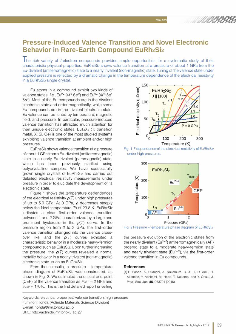
Electronic Materials IMR KINKEN Research Highlights 2017
39IMR KINKEN Research Highlights 2017
Eu atoms in a compound exhibit two kinds of valence states, i.e., Eu2+ (4f 7 6s 2) and Eu3+ (4f 6 5d1 6s2). Most of the Eu compounds are in the divalent electronic state and order magnetically, while some Eu compounds are in the trivalent electronic state. Eu valence can be tuned by temperature, magnetic field, and pressure. In particular, pressure-induced valence transition has attracted much attention for their unique electronic states. EuT2X2 (T: transition metal, X: Si, Ge) is one of the most studied systems exhibiting valence transition at ambient and/or high pressures.
EuRh2Si2 shows valence transition at a pressure of about 1 GPa from a Eu-divalent (antiferromagnetic) state to a nearly Eu-trivalent (paramagnetic) state, which has been previously clarified using polycrystalline samples. We have successfully grown single crystals of EuRh2Si2 and carried out detailed electrical resistivity measurements under pressure in order to elucidate the development of its electronic state.
Figure 1 shows the temperature dependences of the electrical resistivity ρ(T) under high pressures of up to 5.0 GPa. At 0 GPa, ρ decreases steeply below the Néel temperature TN of 23.8 K. EuRh2Si2 indicates a clear first–order valence transition between 1 and 2 GPa, characterized by a large and prominent hysteresis in the ρ(T) curve. In the pressure region from 2 to 3 GPa, the first–order valence transition changed into the valence cross-over like, and the ρ(T) curves exhibited a characteristic behavior in a moderate heavy-fermion compound such as EuIr2Si2. Upon further increasing the pressure, the ρ(T) curves revealed a normal metallic behavior in a nearly trivalent (non-magnetic) electronic state such as EuCo2Si2.
From these results, a pressure – temperature phase diagram of EuRh2Si2 was constructed, as shown in Fig. 2. We estimated the critical end point (CEP) of the valence transition as PCEP ~ 2 GPa and TCEP ~ 170 K. This is the first detailed report unveiling
the pressure evolution of the electronic states from the nearly divalent (Eu2+δ) antiferromagnetically (AF) ordered state to a moderate heavy-fermion state and nearly trivalent state (Eu3-δ’), via the first-order valence transition in Eu compounds.
References[1] F. Honda, K. Okauchi, A. Nakamura, D. X. Li, D. Aoki, H.
Akamine, Y. Ashitomi, M. Hedo, T. Nakama, and Y. Onuki, J.
Phys. Soc. Jpn. 85, 063701 (2016).
Pressure-Induced Valence Transition and Novel Electronic Behavior in Rare-Earth Compound EuRh2Si2The rich variety of f-electron compounds provides ample opportunities for a systematic study of their characteristic physical properties. EuRh2Si2 shows valence transition at a pressure of about 1 GPa from the Eu-divalent (antiferromagnetic) state to a nearly trivalent (non-magnetic) state. Tuning of the valence state under applied pressure is reflected by a dramatic change in the temperature dependence of the electrical resistivity in a EuRh2Si2 single crystal.
Keywords: electrical properties, valence transition, high pressureFuminori Honda (Actinide Materials Science Division)E-mail: [email protected]: http://actinide.imr.tohoku.ac.jp/
Fig. 1 T-dependence of the electrical resistivity of EuRh2Si2 under high pressures.
Fig. 2 Pressure – temperature phase diagram of EuRh2Si2.
150
100
50
0Ele
ctric
al r
esis
tivity
(µΩ
. cm
)3002001000
EuRh2Si2J || [100]
P = 0 GPa
1.0
1.3
2.1 3.23.9
TN
Tv
Tv4.5 5.0
Temperature (K)
Tmax
300
200
100
0
Tem
pera
ture
(K
)
210
Pressure (GPa)
TN
TV
Tmax
EuRh2Si2
AF
CEP
Eu3-δ’
Eu2+δ


Research Centers
IMR KINKEN Research Highlights 2017Research
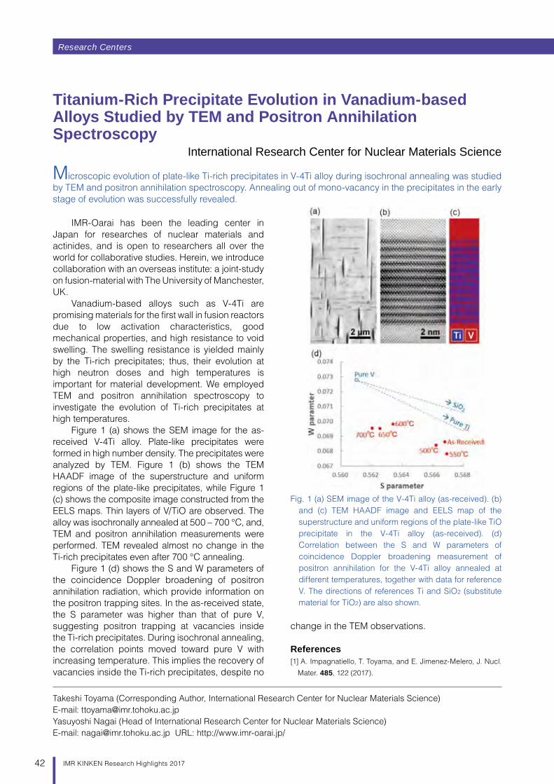
Research Centers
42 IMR KINKEN Research Highlights 2017
IMR-Oarai has been the leading center in Japan for researches of nuclear materials and actinides, and is open to researchers all over the world for collaborative studies. Herein, we introduce collaboration with an overseas institute: a joint-study on fusion-material with The University of Manchester, UK.
Vanadium-based alloys such as V-4Ti are promising materials for the first wall in fusion reactors due to low activation characteristics, good mechanical properties, and high resistance to void swelling. The swelling resistance is yielded mainly by the Ti-rich precipitates; thus, their evolution at high neutron doses and high temperatures is important for material development. We employed TEM and positron annihilation spectroscopy to investigate the evolution of Ti-rich precipitates at high temperatures.
Figure 1 (a) shows the SEM image for the as-received V-4Ti alloy. Plate-like precipitates were formed in high number density. The precipitates were analyzed by TEM. Figure 1 (b) shows the TEM HAADF image of the superstructure and uniform regions of the plate-like precipitates, while Figure 1 (c) shows the composite image constructed from the EELS maps. Thin layers of V/TiO are observed. The alloy was isochronally annealed at 500 – 700 °C, and, TEM and positron annihilation measurements were performed. TEM revealed almost no change in the Ti-rich precipitates even after 700 °C annealing.
Figure 1 (d) shows the S and W parameters of the coincidence Doppler broadening of positron annihilation radiation, which provide information on the positron trapping sites. In the as-received state, the S parameter was higher than that of pure V, suggesting positron trapping at vacancies inside the Ti-rich precipitates. During isochronal annealing, the correlation points moved toward pure V with increasing temperature. This implies the recovery of vacancies inside the Ti-rich precipitates, despite no
change in the TEM observations.
References[1] A. Impagnatiello, T. Toyama, and E. Jimenez-Melero, J. Nucl.
Mater. 485, 122 (2017).
Titanium-Rich Precipitate Evolution in Vanadium-based Alloys Studied by TEM and Positron Annihilation Spectroscopy
International Research Center for Nuclear Materials Science
Microscopic evolution of plate-like Ti-rich precipitates in V-4Ti alloy during isochronal annealing was studied by TEM and positron annihilation spectroscopy. Annealing out of mono-vacancy in the precipitates in the early stage of evolution was successfully revealed.
Takeshi Toyama (Corresponding Author, International Research Center for Nuclear Materials Science)E-mail: [email protected] Nagai (Head of International Research Center for Nuclear Materials Science)E-mail: [email protected] URL: http://www.imr-oarai.jp/
Fig. 1 (a) SEM image of the V-4Ti alloy (as-received). (b) and (c) TEM HAADF image and EELS map of the superstructure and uniform regions of the plate-like TiO precipitate in the V-4Ti alloy (as-received). (d) Correlation between the S and W parameters of coincidence Doppler broadening measurement of positron annihilation for the V-4Ti alloy annealed at different temperatures, together with data for reference V. The directions of references Ti and SiO2 (substitute material for TiO2) are also shown.
Research Centers IMR KINKEN Research Highlights 2017
43IMR KINKEN Research Highlights 2017
In actinide based heavy-fermion compounds, the 5f electrons acquire huge effective masses 100-1000 times larger than that of ordinary conduction electrons, and thus move very slowly in a crystal lattice. In this situation, it is widely considered that Cooper pairs of heavy electrons favor nodal gap symmetry to avoid strong Coulomb repulsions, instead of isotropic s-wave superconductivity. The determination of SC gap structure is of primary importance for the exploration of non-phononic pairing mechanisms, since the angular dependence of the gap function is directly related to the pairing interaction. However, the determination of SC gap symmetry in uranium systems is by no means an easy task; there have been numerous experimental and theoretical works for over thirty years. For example, the true nature of the SC gap in the oldest uranium heavy-fermion superconductor, UBe13, has been unraveled very recently [1].
In the present study [2], we have examined the SC gap symmetry of the hexagonal heavy-fermion antiferromagnet UPd2Al3, in which the antiferromagnetic order coexists with the SC state. We have measured the field-orientation dependences of the heat capacity (C) in order to elucidate the SC gap structure from the viewpoint of the heavy-electron density of states. Figure 1 shows the anisotropic C(H)∝H1/2 behaviors and the two-fold oscillation in the polar angle (θ) dependence of C/T below 1 T in the SC state (T = 0.20 K). Moreover, we found the evolution of a novel anomaly in C(θ) around 45° at intermediate magnetic fields (1 < µ0H < 2 T) [Fig. 1(b)]. These experimental data provide strong thermodynamic evidence for a horizontal line node in heavy-electron bands (Fig. 2). The results obtained by our high-precision experiments using a high-quality single crystal can provide crucial indications for revealing the unconventional pairing mechanisms in uranium heavy-fermion systems.
References[1] Y. Shimizu, S. Kittaka, T. Sakakibara, Y. Haga, E. Yamamoto,
H. Amitsuka, Y. Tsutsumi, and K. Machida, Phys. Rev. Lett. 114,
147002 (2015).
[2] Y. Shimizu, S. Kittaka, T. Sakakibara, Y. Tsutsumi, T. Nomoto,
H. Ikeda, K. Machida, Y. Homma, and D. Aoki, Phys. Rev. Lett.
117, 037001 (2016).
Determination of Superconducting Gap Structure in the Heavy-Fermion Antiferromagnet UPd2Al3
International Research Center for Nuclear Materials Science
The understanding of superconducting (SC) nature in heavy-fermion compounds is one of the recent hot topics of the strongly correlated electron systems. We have recently studied the SC gap symmetry in the heavy-fermion antiferromagnet UPd2Al3 by means of angle-resolved heat–capacity measurements at low temperatures down to 0.1 K using a high-quality single crystal. Our results demonstrate that the field-orientation dependence of heat capacity has a sufficiently high sensitivity to detect a horizontal line nodal gap structure in heavy bands.
Yusei Shimizu (Corresponding Author, International Research Center for Nuclear Materials Science)E-mail: [email protected] Nagai (Head of International Research Center for Nuclear Materials Science)E-mail: [email protected]: http://www.imr-oarai.jp/
Fig. 1 (a) The magnetic field (H) and (b) polar-angle (θ) dependences of heat capacity (C/T) in UPd2Al3 measured at 0.20 K in the hexagonal ac plane (µ0Hc2 ~ 3.2 T) [2]. The inset shows H1/2 dependence of C/T in low fields.
Fig. 2 The SC gap structure in UPd2Al3 with a horizontal line node on the Fermi surface.
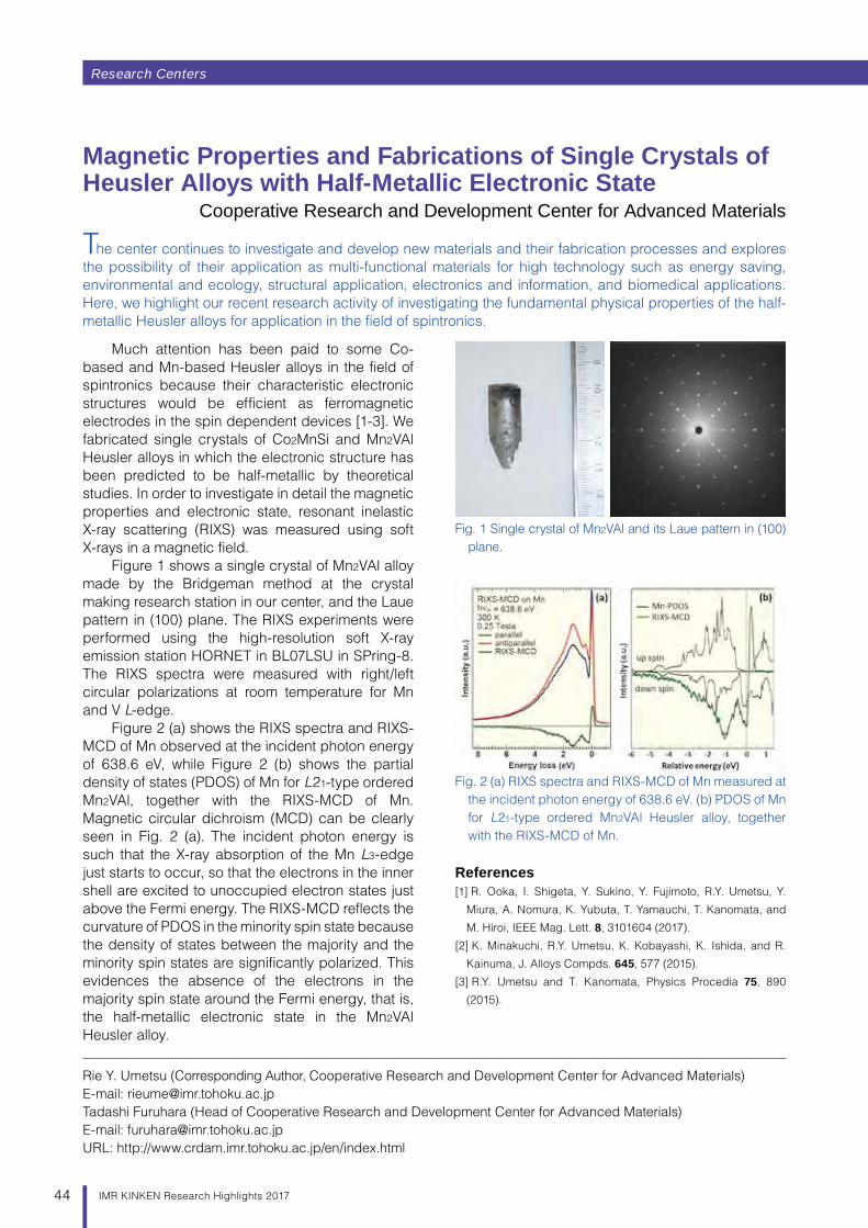
Research Centers
44 IMR KINKEN Research Highlights 2017
Much attention has been paid to some Co-based and Mn-based Heusler alloys in the field of spintronics because their characteristic electronic structures would be efficient as ferromagnetic electrodes in the spin dependent devices [1-3]. We fabricated single crystals of Co2MnSi and Mn2VAl Heusler alloys in which the electronic structure has been predicted to be half-metallic by theoretical studies. In order to investigate in detail the magnetic properties and electronic state, resonant inelastic X-ray scattering (RIXS) was measured using soft X-rays in a magnetic field.
Figure 1 shows a single crystal of Mn2VAl alloy made by the Bridgeman method at the crystal making research station in our center, and the Laue pattern in (100) plane. The RIXS experiments were performed using the high-resolution soft X-ray emission station HORNET in BL07LSU in SPring-8. The RIXS spectra were measured with right/left circular polarizations at room temperature for Mn and V L-edge.
Figure 2 (a) shows the RIXS spectra and RIXS-MCD of Mn observed at the incident photon energy of 638.6 eV, while Figure 2 (b) shows the partial density of states (PDOS) of Mn for L21-type ordered Mn2VAl, together with the RIXS-MCD of Mn. Magnetic circular dichroism (MCD) can be clearly seen in Fig. 2 (a). The incident photon energy is such that the X-ray absorption of the Mn L3-edge just starts to occur, so that the electrons in the inner shell are excited to unoccupied electron states just above the Fermi energy. The RIXS-MCD reflects the curvature of PDOS in the minority spin state because the density of states between the majority and the minority spin states are significantly polarized. This evidences the absence of the electrons in the majority spin state around the Fermi energy, that is, the half-metallic electronic state in the Mn2VAl Heusler alloy.
References[1] R. Ooka, I. Shigeta, Y. Sukino, Y. Fujimoto, R.Y. Umetsu, Y.
Miura, A. Nomura, K. Yubuta, T. Yamauchi, T. Kanomata, and
M. Hiroi, IEEE Mag. Lett. 8, 3101604 (2017).
[2] K. Minakuchi, R.Y. Umetsu, K. Kobayashi, K. Ishida, and R.
Kainuma, J. Alloys Compds. 645, 577 (2015).
[3] R.Y. Umetsu and T. Kanomata, Physics Procedia 75, 890
(2015).
Magnetic Properties and Fabrications of Single Crystals of Heusler Alloys with Half-Metallic Electronic State
Cooperative Research and Development Center for Advanced Materials
The center continues to investigate and develop new materials and their fabrication processes and explores the possibility of their application as multi-functional materials for high technology such as energy saving, environmental and ecology, structural application, electronics and information, and biomedical applications. Here, we highlight our recent research activity of investigating the fundamental physical properties of the half-metallic Heusler alloys for application in the field of spintronics.
Rie Y. Umetsu (Corresponding Author, Cooperative Research and Development Center for Advanced Materials)E-mail: [email protected] Furuhara (Head of Cooperative Research and Development Center for Advanced Materials)E-mail: [email protected]: http://www.crdam.imr.tohoku.ac.jp/en/index.html
Fig. 1 Single crystal of Mn2VAl and its Laue pattern in (100) plane.
Fig. 2 (a) RIXS spectra and RIXS-MCD of Mn measured at the incident photon energy of 638.6 eV. (b) PDOS of Mn for L21-type ordered Mn2VAl Heusler alloy, together with the RIXS-MCD of Mn.
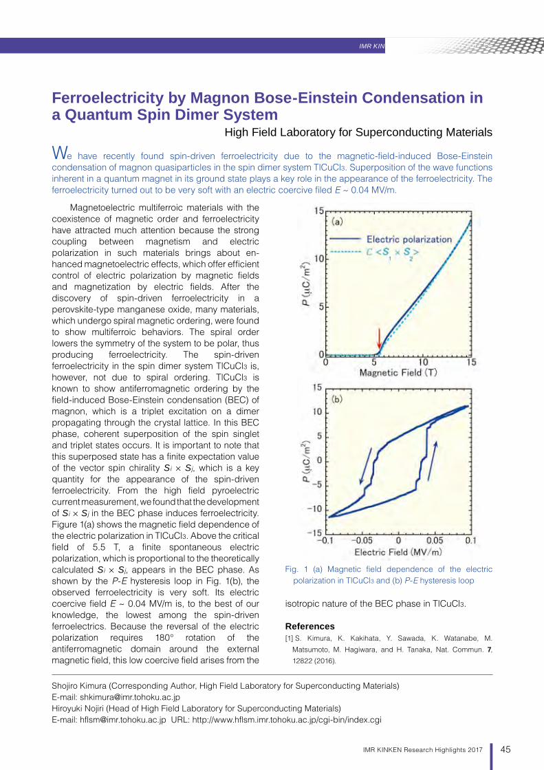
Research Centers IMR KINKEN Research Highlights 2017
45IMR KINKEN Research Highlights 2017
Magnetoelectric multiferroic materials with the coexistence of magnetic order and ferroelectricity have attracted much attention because the strong coupling between magnetism and electric polarization in such materials brings about en-hanced magnetoelectric effects, which offer efficient control of electric polarization by magnetic fields and magnetization by electric fields. After the discovery of spin-driven ferroelectricity in a perovskite-type manganese oxide, many materials, which undergo spiral magnetic ordering, were found to show multiferroic behaviors. The spiral order lowers the symmetry of the system to be polar, thus producing ferroelectricity. The spin-driven ferroelectricity in the spin dimer system TlCuCl3 is, however, not due to spiral ordering. TlCuCl3 is known to show antiferromagnetic ordering by the field-induced Bose-Einstein condensation (BEC) of magnon, which is a triplet excitation on a dimer propagating through the crystal lattice. In this BEC phase, coherent superposition of the spin singlet and triplet states occurs. It is important to note that this superposed state has a finite expectation value of the vector spin chirality Si × Sj, which is a key quantity for the appearance of the spin-driven ferroelectricity. From the high field pyroelectric current measurement, we found that the development of Si × Sj in the BEC phase induces ferroelectricity. Figure 1(a) shows the magnetic field dependence of the electric polarization in TlCuCl3. Above the critical field of 5.5 T, a finite spontaneous electric polarization, which is proportional to the theoretically calculated Si × Sj, appears in the BEC phase. As shown by the P-E hysteresis loop in Fig. 1(b), the observed ferroelectricity is very soft. Its electric coercive field E ~ 0.04 MV/m is, to the best of our knowledge, the lowest among the spin-driven ferroelectrics. Because the reversal of the electric polarization requires 180° rotation of the antiferromagnetic domain around the external magnetic field, this low coercive field arises from the
isotropic nature of the BEC phase in TlCuCl3.
References[1] S. Kimura, K. Kakihata, Y. Sawada, K. Watanabe, M.
Matsumoto, M. Hagiwara, and H. Tanaka, Nat. Commun. 7,
12822 (2016).
Ferroelectricity by Magnon Bose-Einstein Condensation in a Quantum Spin Dimer System
High Field Laboratory for Superconducting Materials
We have recently found spin-driven ferroelectricity due to the magnetic-field-induced Bose-Einstein condensation of magnon quasiparticles in the spin dimer system TlCuCl3. Superposition of the wave functions inherent in a quantum magnet in its ground state plays a key role in the appearance of the ferroelectricity. The ferroelectricity turned out to be very soft with an electric coercive filed E ~ 0.04 MV/m.
Shojiro Kimura (Corresponding Author, High Field Laboratory for Superconducting Materials)E-mail: [email protected] Nojiri (Head of High Field Laboratory for Superconducting Materials)E-mail: [email protected] URL: http://www.hflsm.imr.tohoku.ac.jp/cgi-bin/index.cgi
Fig. 1 (a) Magnetic field dependence of the electric polarization in TlCuCl3 and (b) P-E hysteresis loop
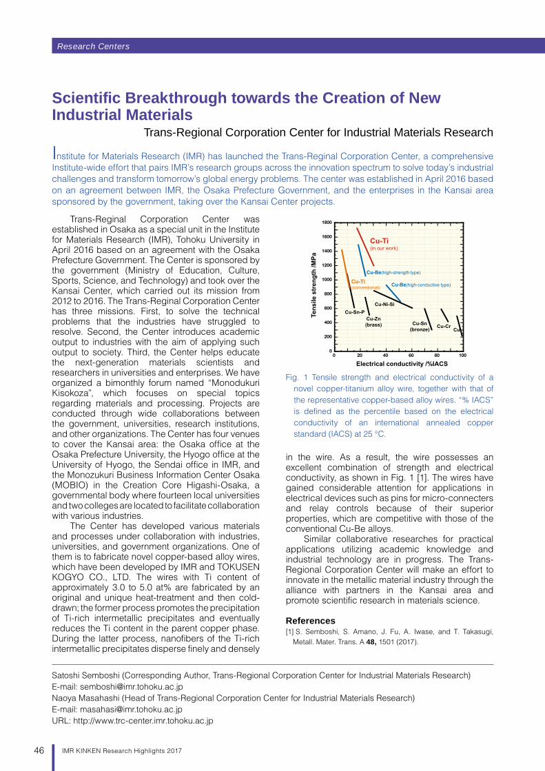
Research Centers
46 IMR KINKEN Research Highlights 2017
Trans-Reginal Corporation Center was established in Osaka as a special unit in the Institute for Materials Research (IMR), Tohoku University in April 2016 based on an agreement with the Osaka Prefecture Government. The Center is sponsored by the government (Ministry of Education, Culture, Sports, Science, and Technology) and took over the Kansai Center, which carried out its mission from 2012 to 2016. The Trans-Reginal Corporation Center has three missions. First, to solve the technical problems that the industries have struggled to resolve. Second, the Center introduces academic output to industries with the aim of applying such output to society. Third, the Center helps educate the next-generation materials scientists and researchers in universities and enterprises. We have organized a bimonthly forum named “Monodukuri Kisokoza”, which focuses on special topics regarding materials and processing. Projects are conducted through wide collaborations between the government, universities, research institutions, and other organizations. The Center has four venues to cover the Kansai area: the Osaka office at the Osaka Prefecture University, the Hyogo office at the University of Hyogo, the Sendai office in IMR, and the Monozukuri Business Information Center Osaka (MOBIO) in the Creation Core Higashi-Osaka, a governmental body where fourteen local universities and two colleges are located to facilitate collaboration with various industries.
The Center has developed various materials and processes under collaboration with industries, universities, and government organizations. One of them is to fabricate novel copper-based alloy wires, which have been developed by IMR and TOKUSEN KOGYO CO., LTD. The wires with Ti content of approximately 3.0 to 5.0 at% are fabricated by an original and unique heat-treatment and then cold-drawn; the former process promotes the precipitation of Ti-rich intermetallic precipitates and eventually reduces the Ti content in the parent copper phase. During the latter process, nanofibers of the Ti-rich intermetallic precipitates disperse finely and densely
in the wire. As a result, the wire possesses an excellent combination of strength and electrical conductivity, as shown in Fig. 1 [1]. The wires have gained considerable attention for applications in electrical devices such as pins for micro-connecters and relay controls because of their superior properties, which are competitive with those of the conventional Cu-Be alloys.
Similar collaborative researches for practical applications utilizing academic knowledge and industrial technology are in progress. The Trans-Regional Corporation Center will make an effort to innovate in the metallic material industry through the alliance with partners in the Kansai area and promote scientific research in materials science.
References[1] S. Semboshi, S. Amano, J. Fu, A. Iwase, and T. Takasugi,
Metall. Mater. Trans. A 48, 1501 (2017).
Scientific Breakthrough towards the Creation of New Industrial Materials
Trans-Regional Corporation Center for Industrial Materials Research
Institute for Materials Research (IMR) has launched the Trans-Reginal Corporation Center, a comprehensive Institute-wide effort that pairs IMR’s research groups across the innovation spectrum to solve today’s industrial challenges and transform tomorrow’s global energy problems. The center was established in April 2016 based on an agreement between IMR, the Osaka Prefecture Government, and the enterprises in the Kansai area sponsored by the government, taking over the Kansai Center projects.
Satoshi Semboshi (Corresponding Author, Trans-Regional Corporation Center for Industrial Materials Research)E-mail: [email protected] Masahashi (Head of Trans-Regional Corporation Center for Industrial Materials Research)E-mail: [email protected]: http://www.trc-center.imr.tohoku.ac.jp
Fig. 1 Tensile strength and electrical conductivity of a novel copper-titanium alloy wire, together with that of the representative copper-based alloy wires. “% IACS” is defined as the percentile based on the electrical conductivity of an international annealed copper standard (IACS) at 25 °C.
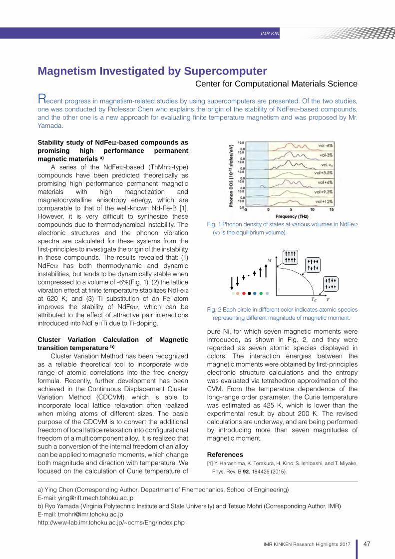
Research Centers IMR KINKEN Research Highlights 2017
47IMR KINKEN Research Highlights 2017
Stability study of NdFe12-based compounds as promising high performance permanent magnetic materials a)
A series of the NdFe12-based (ThMn12-type) compounds have been predicted theoretically as promising high performance permanent magnetic materials with high magnetization and magnetocrystalline anisotropy energy, which are comparable to that of the well-known Nd-Fe-B [1]. However, it is very difficult to synthesize these compounds due to thermodynamical instability. The electronic structures and the phonon vibration spectra are calculated for these systems from the first-principles to investigate the origin of the instability in these compounds. The results revealed that: (1) NdFe12 has both thermodynamic and dynamic instabilities, but tends to be dynamically stable when compressed to a volume of -6%(Fig. 1); (2) the lattice vibration effect at finite temperature stabilizes NdFe12 at 620 K; and (3) Ti substitution of an Fe atom improves the stability of NdFe12, which can be attributed to the effect of attractive pair interactions introduced into NdFe11Ti due to Ti-doping.
Cluster Variation Calculation of Magnetic transition temperature b)
Cluster Variation Method has been recognized as a reliable theoretical tool to incorporate wide range of atomic correlations into the free energy formula. Recently, further development has been achieved in the Continuous Displacement Cluster Variation Method (CDCVM), which is able to incorporate local lattice relaxation often realized when mixing atoms of different sizes. The basic purpose of the CDCVM is to convert the additional freedom of local lattice relaxation into configurational freedom of a multicomponent alloy. It is realized that such a conversion of the internal freedom of an alloy can be applied to magnetic moments, which change both magnitude and direction with temperature. We focused on the calculation of Curie temperature of
pure Ni, for which seven magnetic moments were introduced, as shown in Fig. 2, and they were regarded as seven atomic species displayed in colors. The interaction energies between the magnetic moments were obtained by first-principles electronic structure calculations and the entropy was evaluated via tetrahedron approximation of the CVM. From the temperature dependence of the long-range order parameter, the Curie temperature was estimated as 425 K, which is lower than the experimental result by about 200 K. The revised calculations are underway, and are being performed by introducing more than seven magnitudes of magnetic moment.
References[1] Y. Harashima, K. Terakura, H. Kino, S. Ishibashi, and T. Miyake,
Phys. Rev. B 92, 184426 (2015).
Magnetism Investigated by SupercomputerCenter for Computational Materials Science
Recent progress in magnetism-related studies by using supercomputers are presented. Of the two studies, one was conducted by Professor Chen who explains the origin of the stability of NdFe12-based compounds, and the other one is a new approach for evaluating finite temperature magnetism and was proposed by Mr. Yamada.
a) Ying Chen (Corresponding Author, Department of Finemechanics, School of Engineering)E-mail: [email protected]) Ryo Yamada (Virginia Polytechnic Institute and State University) and Tetsuo Mohri (Corresponding Author, IMR)E-mail: [email protected]://www-lab.imr.tohoku.ac.jp/~ccms/Eng/index.php
Fig. 1 Phonon density of states at various volumes in NdFe12 (v0 is the equilibrium volume).
Fig. 2 Each circle in different color indicates atomic species representing different magnitude of magnetic moment.
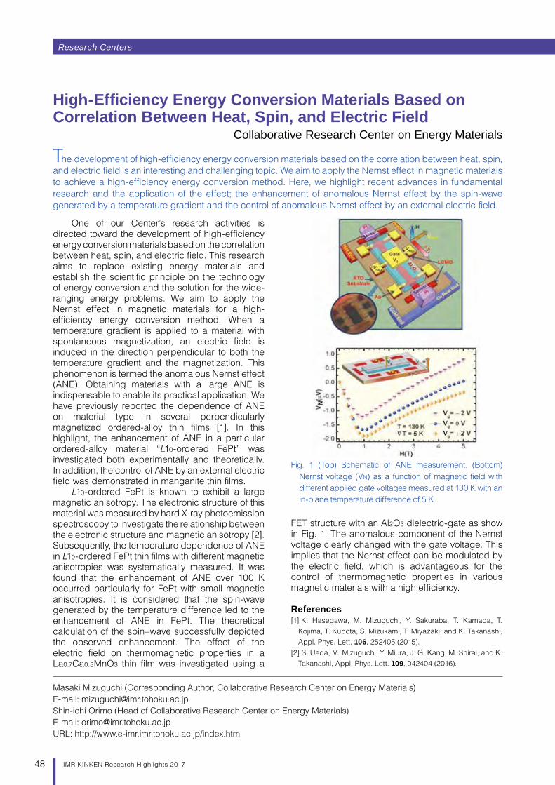
Research Centers
48 IMR KINKEN Research Highlights 2017
One of our Center’s research activities is directed toward the development of high-efficiency energy conversion materials based on the correlation between heat, spin, and electric field. This research aims to replace existing energy materials and establish the scientific principle on the technology of energy conversion and the solution for the wide-ranging energy problems. We aim to apply the Nernst effect in magnetic materials for a high-efficiency energy conversion method. When a temperature gradient is applied to a material with spontaneous magnetization, an electric field is induced in the direction perpendicular to both the temperature gradient and the magnetization. This phenomenon is termed the anomalous Nernst effect (ANE). Obtaining materials with a large ANE is indispensable to enable its practical application. We have previously reported the dependence of ANE on material type in several perpendicularly magnetized ordered-alloy thin films [1]. In this highlight, the enhancement of ANE in a particular ordered-alloy material “L10-ordered FePt” was investigated both experimentally and theoretically. In addition, the control of ANE by an external electric field was demonstrated in manganite thin films.
L10-ordered FePt is known to exhibit a large magnetic anisotropy. The electronic structure of this material was measured by hard X-ray photoemission spectroscopy to investigate the relationship between the electronic structure and magnetic anisotropy [2]. Subsequently, the temperature dependence of ANE in L10-ordered FePt thin films with different magnetic anisotropies was systematically measured. It was found that the enhancement of ANE over 100 K occurred particularly for FePt with small magnetic anisotropies. It is considered that the spin-wave generated by the temperature difference led to the enhancement of ANE in FePt. The theoretical calculation of the spin–wave successfully depicted the observed enhancement. The effect of the electric field on thermomagnetic properties in a La0.7Ca0.3MnO3 thin film was investigated using a
FET structure with an Al2O3 dielectric-gate as show in Fig. 1. The anomalous component of the Nernst voltage clearly changed with the gate voltage. This implies that the Nernst effect can be modulated by the electric field, which is advantageous for the control of thermomagnetic properties in various magnetic materials with a high efficiency.
References[1] K. Hasegawa, M. Mizuguchi, Y. Sakuraba, T. Kamada, T.
Kojima, T. Kubota, S. Mizukami, T. Miyazaki, and K. Takanashi, Appl. Phys. Lett. 106, 252405 (2015).
[2] S. Ueda, M. Mizuguchi, Y. Miura, J. G. Kang, M. Shirai, and K. Takanashi, Appl. Phys. Lett. 109, 042404 (2016).
High-Efficiency Energy Conversion Materials Based on Correlation Between Heat, Spin, and Electric Field
Collaborative Research Center on Energy Materials
The development of high-efficiency energy conversion materials based on the correlation between heat, spin, and electric field is an interesting and challenging topic. We aim to apply the Nernst effect in magnetic materials to achieve a high-efficiency energy conversion method. Here, we highlight recent advances in fundamental research and the application of the effect; the enhancement of anomalous Nernst effect by the spin-wave generated by a temperature gradient and the control of anomalous Nernst effect by an external electric field.
Masaki Mizuguchi (Corresponding Author, Collaborative Research Center on Energy Materials)E-mail: [email protected] Orimo (Head of Collaborative Research Center on Energy Materials)E-mail: [email protected]: http://www.e-imr.imr.tohoku.ac.jp/index.html
Fig. 1 (Top) Schematic of ANE measurement. (Bottom) Nernst voltage (VN) as a function of magnetic field with different applied gate voltages measured at 130 K with an in-plane temperature difference of 5 K.
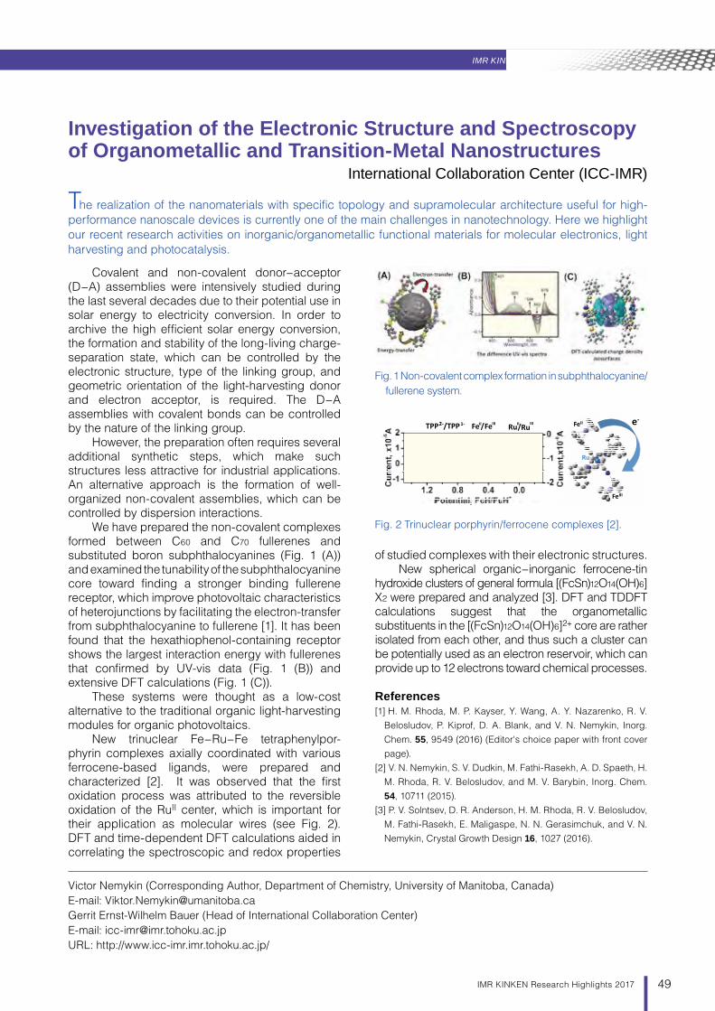
Research Centers IMR KINKEN Research Highlights 2017
49IMR KINKEN Research Highlights 2017
Covalent and non-covalent donor−acceptor (D−A) assemblies were intensively studied during the last several decades due to their potential use in solar energy to electricity conversion. In order to archive the high efficient solar energy conversion, the formation and stability of the long-living charge-separation state, which can be controlled by the electronic structure, type of the linking group, and geometric orientation of the light-harvesting donor and electron acceptor, is required. The D−A assemblies with covalent bonds can be controlled by the nature of the linking group.
However, the preparation often requires several additional synthetic steps, which make such structures less attractive for industrial applications. An alternative approach is the formation of well-organized non-covalent assemblies, which can be controlled by dispersion interactions.
We have prepared the non-covalent complexes formed between C60 and C70 fullerenes and substituted boron subphthalocyanines (Fig. 1 (A)) and examined the tunability of the subphthalocyanine core toward finding a stronger binding fullerene receptor, which improve photovoltaic characteristics of heterojunctions by facilitating the electron-transfer from subphthalocyanine to fullerene [1]. It has been found that the hexathiophenol-containing receptor shows the largest interaction energy with fullerenes that confirmed by UV-vis data (Fig. 1 (B)) and extensive DFT calculations (Fig. 1 (C)).
These systems were thought as a low-cost alternative to the traditional organic light-harvesting modules for organic photovoltaics.
New trinuclear Fe−Ru−Fe tetraphenylpor- phyrin complexes axially coordinated with various ferrocene-based ligands, were prepared and characterized [2]. It was observed that the first oxidation process was attributed to the reversible oxidation of the RuII center, which is important for their application as molecular wires (see Fig. 2). DFT and time-dependent DFT calculations aided in correlating the spectroscopic and redox properties
of studied complexes with their electronic structures.New spherical organic−inorganic ferrocene-tin
hydroxide clusters of general formula [(FcSn)12O14(OH)6]X2 were prepared and analyzed [3]. DFT and TDDFT calculations suggest that the organometallic substituents in the [(FcSn)12O14(OH)6]2+ core are rather isolated from each other, and thus such a cluster can be potentially used as an electron reservoir, which can provide up to 12 electrons toward chemical processes.
References[1] H. M. Rhoda, M. P. Kayser, Y. Wang, A. Y. Nazarenko, R. V.
Belosludov, P. Kiprof, D. A. Blank, and V. N. Nemykin, Inorg.
Chem. 55, 9549 (2016) (Editor's choice paper with front cover
page).
[2] V. N. Nemykin, S. V. Dudkin, M. Fathi-Rasekh, A. D. Spaeth, H.
M. Rhoda, R. V. Belosludov, and M. V. Barybin, Inorg. Chem.
54, 10711 (2015).
[3] P. V. Solntsev, D. R. Anderson, H. M. Rhoda, R. V. Belosludov,
M. Fathi-Rasekh, E. Maligaspe, N. N. Gerasimchuk, and V. N.
Nemykin, Crystal Growth Design 16, 1027 (2016).
Investigation of the Electronic Structure and Spectroscopy of Organometallic and Transition-Metal Nanostructures
International Collaboration Center (ICC-IMR)
The realization of the nanomaterials with specific topology and supramolecular architecture useful for high-performance nanoscale devices is currently one of the main challenges in nanotechnology. Here we highlight our recent research activities on inorganic/organometallic functional materials for molecular electronics, light harvesting and photocatalysis.
Victor Nemykin (Corresponding Author, Department of Chemistry, University of Manitoba, Canada)E-mail: [email protected] Ernst-Wilhelm Bauer (Head of International Collaboration Center)E-mail: [email protected]: http://www.icc-imr.imr.tohoku.ac.jp/
Fig. 1 Non-covalent complex formation in subphthalocyanine/fullerene system.
Fig. 2 Trinuclear porphyrin/ferrocene complexes [2].
TPP2-/TPP1- FeII/FeIII RuII/RuIII FeII
FeIII
Ru
e-
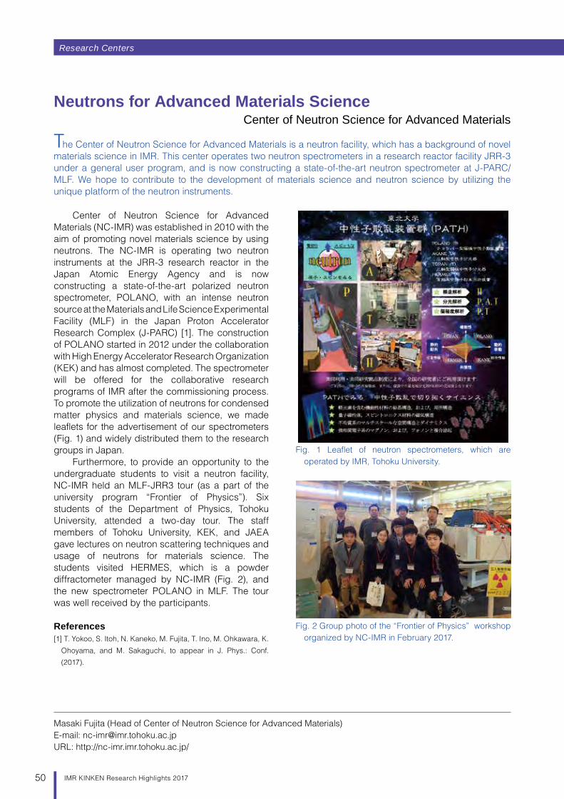
Research Centers
50 IMR KINKEN Research Highlights 2017
Center of Neutron Science for Advanced Materials (NC-IMR) was established in 2010 with the aim of promoting novel materials science by using neutrons. The NC-IMR is operating two neutron instruments at the JRR-3 research reactor in the Japan Atomic Energy Agency and is now constructing a state-of-the-art polarized neutron spectrometer, POLANO, with an intense neutron source at the Materials and Life Science Experimental Facility (MLF) in the Japan Proton Accelerator Research Complex (J-PARC) [1]. The construction of POLANO started in 2012 under the collaboration with High Energy Accelerator Research Organization (KEK) and has almost completed. The spectrometer will be offered for the collaborative research programs of IMR after the commissioning process. To promote the utilization of neutrons for condensed matter physics and materials science, we made leaflets for the advertisement of our spectrometers (Fig. 1) and widely distributed them to the research groups in Japan.
Furthermore, to provide an opportunity to the undergraduate students to visit a neutron facility, NC-IMR held an MLF-JRR3 tour (as a part of the university program “Frontier of Physics”). Six students of the Department of Physics, Tohoku University, attended a two-day tour. The staff members of Tohoku University, KEK, and JAEA gave lectures on neutron scattering techniques and usage of neutrons for materials science. The students visited HERMES, which is a powder diffractometer managed by NC-IMR (Fig. 2), and the new spectrometer POLANO in MLF. The tour was well received by the participants.
References[1] T. Yokoo, S. Itoh, N. Kaneko, M. Fujita, T. Ino, M. Ohkawara, K.
Ohoyama, and M. Sakaguchi, to appear in J. Phys.: Conf.
(2017).
Neutrons for Advanced Materials ScienceCenter of Neutron Science for Advanced Materials
The Center of Neutron Science for Advanced Materials is a neutron facility, which has a background of novel materials science in IMR. This center operates two neutron spectrometers in a research reactor facility JRR-3 under a general user program, and is now constructing a state-of-the-art neutron spectrometer at J-PARC/MLF. We hope to contribute to the development of materials science and neutron science by utilizing the unique platform of the neutron instruments.
Masaki Fujita (Head of Center of Neutron Science for Advanced Materials)E-mail: [email protected]: http://nc-imr.imr.tohoku.ac.jp/
Fig. 1 Leaflet of neutron spectrometers, which are operated by IMR, Tohoku University.
Fig. 2 Group photo of the “Frontier of Physics” workshop organized by NC-IMR in February 2017.
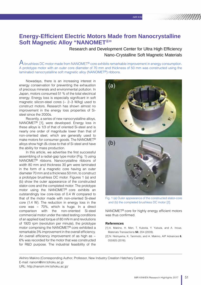
Research Centers IMR KINKEN Research Highlights 2017
51IMR KINKEN Research Highlights 2017
Nowadays, there is an increasing interest in energy conservation for preventing the exhaustion of precious minerals and environmental pollution. In Japan, motors consumed 51 % of the total electrical energy. Energy loss is especially significant in soft magnetic silicon-steel cores (~ 2–3 W/kg) used to construct motors. Research has shown almost no improvement in the energy loss properties of Si-steel since the 2000s.
Recently, a series of new nanocrystalline alloys, NANOMET® [1], were developed. Energy loss in these alloys is 1/3 of that of oriented Si-steel and is nearly one order of magnitude lower than that of non-oriented steel, which are generally used to make motors for consumer goods. The NANOMET® alloys show high Bs close to that of Si-steel and have the ability for mass production.
In this article, we advertise the first successful assembling of a radial-gap type motor (Fig. 1) using NANOMET® ribbons. Nanocrystalline ribbons of width 80 mm and thickness 30 µm were laminated in the form of a magnetic core having an outer diameter 70 mm and a thickness 50 mm, to construct a prototype brushless DC motor. Figures 1 (a) and (b) show the outer appearance of the constructed stator-core and the completed motor. The prototype motor using the NANOMET® core exhibits an outstandingly low core-loss of 0.4 W compared to that of the motor made with non-oriented Si-steel core (1.4 W). The reduction in energy loss in the core was ~ 70%, which is huge. In a direct comparison with the non-oriented Si-steel commercial motor under the rated testing conditions of an applied load torque of 80 mN·m and revolutions of 1920 rpm (revolution per minute), the prototype motor comprising the NANOMET® core exhibited a remarkable 3% improvement in the overall efficiency. An overall efficiency improvement of as high as ~ 6% was recorded for the motor that was constructed for R&D purpose. The industrial feasibility of the
NANOMET® core for highly energy efficient motors was thus confirmed.
References[1] A. Makino, H. Men, T. Kubota, Y. Yubuta, and A. Inoue,
Materials Transactions 50, 204 (2009).
[2] N. Nishiyama, K. Tanimoto, and A. Makino, AIP Advances 6,
055925 (2016).
Energy-Efficient Electric Motors Made from Nanocrystalline Soft Magnetic Alloy “NANOMET®”
Research and Development Center for Ultra High Efficiency Nano-Crystalline Soft Magnetic Materials
A brushless DC motor made from NANOMET® core exhibits remarkable improvement in energy consumption. A prototype motor with an outer core diameter of 70 mm and thickness of 50 mm was constructed using the laminated nanocrystalline soft magnetic alloy (NANOMET®) ribbons.
Akihiro Makino (Corresponding Author, Professor, New Industry Creation Hatchery Center)E-mail: [email protected]: http://nanom.imr.tohoku.ac.jp/
Fig. 1 (a) Outer appearance of the constructed stator-core and (b) the completed brushless DC motor [2].
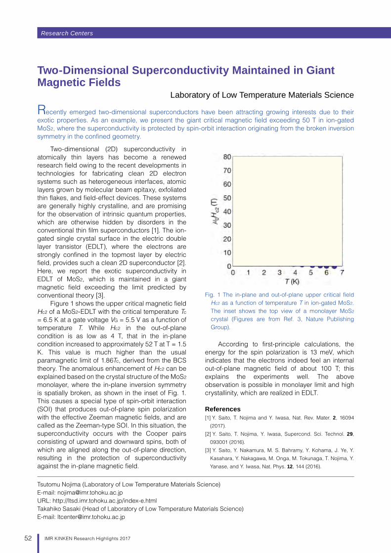
Research Centers
52 IMR KINKEN Research Highlights 2017
Two-dimensional (2D) superconductivity in atomically thin layers has become a renewed research field owing to the recent developments in technologies for fabricating clean 2D electron systems such as heterogeneous interfaces, atomic layers grown by molecular beam epitaxy, exfoliated thin flakes, and field-effect devices. These systems are generally highly crystalline, and are promising for the observation of intrinsic quantum properties, which are otherwise hidden by disorders in the conventional thin film superconductors [1]. The ion-gated single crystal surface in the electric double layer transistor (EDLT), where the electrons are strongly confined in the topmost layer by electric field, provides such a clean 2D superconductor [2]. Here, we report the exotic superconductivity in EDLT of MoS2, which is maintained in a giant magnetic field exceeding the limit predicted by conventional theory [3].
Figure 1 shows the upper critical magnetic field Hc2 of a MoS2-EDLT with the critical temperature Tc = 6.5 K at a gate voltage VG = 5.5 V as a function of temperature T. While Hc2 in the out-of-plane condition is as low as 4 T, that in the in-plane condition increased to approximately 52 T at T = 1.5 K. This value is much higher than the usual paramagnetic limit of 1.86Tc, derived from the BCS theory. The anomalous enhancement of Hc2 can be explained based on the crystal structure of the MoS2 monolayer, where the in-plane inversion symmetry is spatially broken, as shown in the inset of Fig. 1. This causes a special type of spin-orbit interaction (SOI) that produces out-of-plane spin polarization with the effective Zeeman magnetic fields, and are called as the Zeeman-type SOI. In this situation, the superconductivity occurs with the Cooper pairs consisting of upward and downward spins, both of which are aligned along the out-of-plane direction, resulting in the protection of superconductivity against the in-plane magnetic field.
According to first-principle calculations, the energy for the spin polarization is 13 meV, which indicates that the electrons indeed feel an internal out-of-plane magnetic field of about 100 T; this explains the experiments well. The above observation is possible in monolayer limit and high crystallinity, which are realized in EDLT.
References[1] Y. Saito, T. Nojima and Y. Iwasa, Nat. Rev. Mater. 2, 16094
(2017).
[2] Y. Saito, T. Nojima, Y. Iwasa, Supercond. Sci. Technol. 29,
093001 (2016).
[3] Y. Saito, Y. Nakamura, M. S. Bahramy, Y. Kohama, J. Ye, Y.
Kasahara, Y. Nakagawa, M. Onga, M. Tokunaga, T. Nojima, Y.
Yanase, and Y. Iwasa, Nat. Phys. 12, 144 (2016).
Two-Dimensional Superconductivity Maintained in Giant Magnetic Fields
Laboratory of Low Temperature Materials Science
Recently emerged two-dimensional superconductors have been attracting growing interests due to their exotic properties. As an example, we present the giant critical magnetic field exceeding 50 T in ion-gated MoS2, where the superconductivity is protected by spin-orbit interaction originating from the broken inversion symmetry in the confined geometry.
Tsutomu Nojima (Laboratory of Low Temperature Materials Science)E-mail: [email protected]: http://ltsd.imr.tohoku.ac.jp/index-e.htmlTakahiko Sasaki (Head of Laboratory of Low Temperature Materials Science)E-mail: [email protected]
Fig. 1 The in-plane and out-of-plane upper critical field Hc2 as a function of temperature T in ion-gated MoS2. The inset shows the top view of a monolayer MoS2 crystal (Figures are from Ref. 3, Nature Publishing Group).
SeMo
MoS2-EDLTVG = 5.5 V
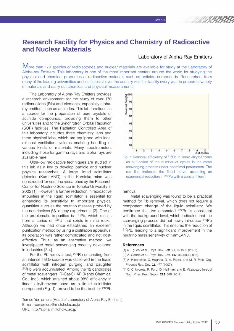
Research Centers IMR KINKEN Research Highlights 2017
53IMR KINKEN Research Highlights 2017
The Laboratory of Alpha-Ray Emitters provides a research environment for the study of over 170 radionuclides (RIs) and elements, especially alpha-ray emitters such as actinides. This lab functions as a source for the preparation of pure crystals of actinide compounds, providing them to other universities and to the Synchrotron Orbital Radiation (SOR) facilities. The Radiation Controlled Area of this laboratory includes three chemistry labs and three physical labs, which are equipped with local exhaust ventilation systems enabling handling of various kinds of materials. Many spectrometers including those for gamma-rays and alpha-rays are available here.
Ultra-low radioactive techniques are studied in this lab as a key to develop particle and nuclear physics researches. A large liquid scintillator detector (KamLAND) in the Kamioka mine was constructed for neutrino researches by the Research Center for Neutrino Science in Tohoku University in 2002 [1]. However, a further reduction in radioactive impurities in the liquid scintillator is essential for enhancing its sensitivity to important physical quantities such as the neutrino masses probed by the neutrinoless ββ–decay experiments [2]. One of the problematic impurities is 210Pb, which results from a series of 238U that exists in mine rocks. Although we had once established an excellent purification method by using a distillation apparatus, its operation was rather complicated and not cost-effective. Thus, as an alternative method, we investigated metal scavenging recently developed in industries [3,4].
For the Pb removal test, 220Rn emanating from an intense ThO2 source was dissolved in the liquid scintillator with nitrogen purging, and daughter 212Pb were accumulated. Among the 12 candidates of metal scavengers, R-Cat-Sil AP (Kanto Chemical Co., Inc.), which attained about 98% efficiency in linear alkylbenzene used as a liquid scintillator component (Fig. 1), proved to be the best for 212Pb
removal.Metal scavenging was found to be a practical
method for Pb removal, which does not require a component change of the liquid scintillator. We confirmed that the emanated 222Rn is consistent with the background level, which indicates that the scavenging process did not newly introduce 210Pb in the liquid scintillator. This ensured the reduction of 210Pb, leading to a significant improvement in the neutrino mass sensitivity of KamLAND.
References[1] K. Eguchi et al., Phys. Rev. Lett. 90, 021802 (2003).
[2] A. Gando et al., Phys. Rev. Lett. 117, 082503 (2016).
[3] A. Hinchcliffe, C. Hughes, D. A. Pears, and M. R. Pitts, Org.
Process Res. Dev. 11, 477 (2007).
[4] O. Chkvorets, R. Ford, D. Hallman, and E. Vázquez-Jáuregui
Nucl. Phys. Proc. Suppl. 229, 519 (2012).
Research Facility for Physics and Chemistry of Radioactive and Nuclear Materials
Laboratory of Alpha-Ray Emitters
More than 170 species of radioisotopes and nuclear materials are available for study at the Laboratory of Alpha-ray Emitters. This laboratory is one of the most important centers around the world for studying the physical and chemical properties of radioactive materials such as actinide compounds. Researchers from many of the leading universities and institutes all over the country visit this facility every year to prepare a variety of materials and carry out chemical and physical measurements.
Tomoo Yamamura (Head of Laboratory of Alpha-Ray Emitters)E-mail: [email protected]: http://alpha.imr.tohoku.ac.jp
Fig. 1 Removal efficiency of 212Pb in linear alkylbenzene as a function of the number of cycles in the metal scavenging process under optimized parameters. The red line indicates the fitted curve, assuming an exponential reduction in 212Pb with a constant term.
NH2 M + NH2 M
n n
e-
e-
νν
KamLAND
neutrinoless ββ-decay
Metal scavenging process
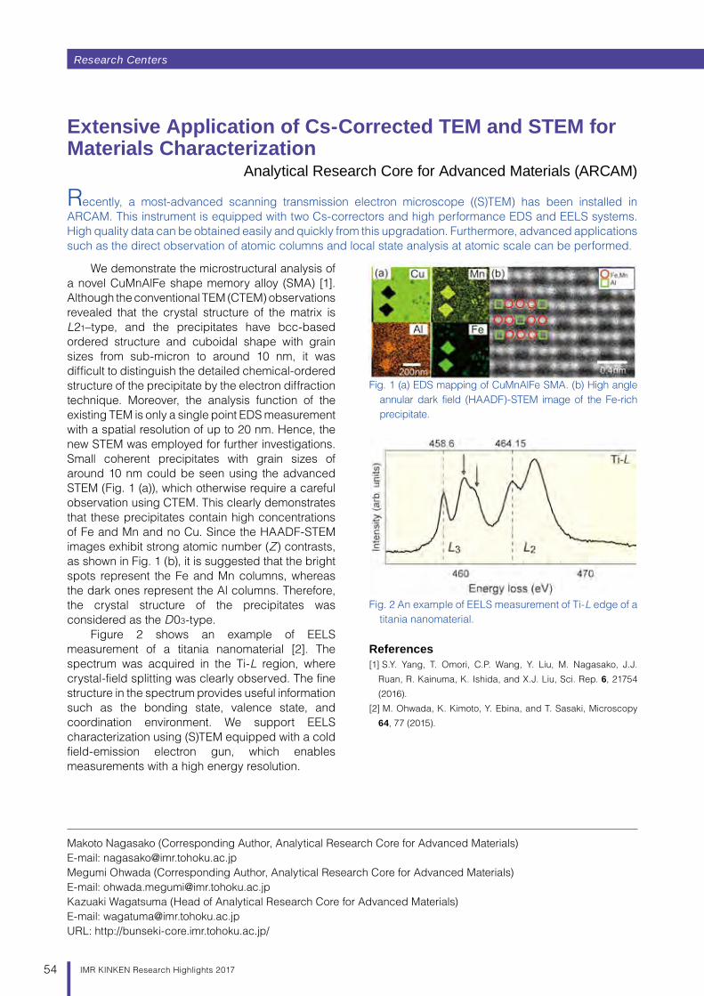
Research Centers
54 IMR KINKEN Research Highlights 2017
We demonstrate the microstructural analysis of a novel CuMnAlFe shape memory alloy (SMA) [1]. Although the conventional TEM (CTEM) observations revealed that the crystal structure of the matrix is L21–type, and the precipitates have bcc-based ordered structure and cuboidal shape with grain sizes from sub-micron to around 10 nm, it was difficult to distinguish the detailed chemical-ordered structure of the precipitate by the electron diffraction technique. Moreover, the analysis function of the existing TEM is only a single point EDS measurement with a spatial resolution of up to 20 nm. Hence, the new STEM was employed for further investigations. Small coherent precipitates with grain sizes of around 10 nm could be seen using the advanced STEM (Fig. 1 (a)), which otherwise require a careful observation using CTEM. This clearly demonstrates that these precipitates contain high concentrations of Fe and Mn and no Cu. Since the HAADF-STEM images exhibit strong atomic number (Z) contrasts, as shown in Fig. 1 (b), it is suggested that the bright spots represent the Fe and Mn columns, whereas the dark ones represent the Al columns. Therefore, the crystal structure of the precipitates was considered as the D03-type.
Figure 2 shows an example of EELS measurement of a titania nanomaterial [2]. The spectrum was acquired in the Ti-L region, where crystal-field splitting was clearly observed. The fine structure in the spectrum provides useful information such as the bonding state, valence state, and coordination environment. We support EELS characterization using (S)TEM equipped with a cold field-emission electron gun, which enables measurements with a high energy resolution.
References[1] S.Y. Yang, T. Omori, C.P. Wang, Y. Liu, M. Nagasako, J.J.
Ruan, R. Kainuma, K. Ishida, and X.J. Liu, Sci. Rep. 6, 21754
(2016).
[2] M. Ohwada, K. Kimoto, Y. Ebina, and T. Sasaki, Microscopy
64, 77 (2015).
Extensive Application of Cs-Corrected TEM and STEM for Materials Characterization
Analytical Research Core for Advanced Materials (ARCAM)
Recently, a most-advanced scanning transmission electron microscope ((S)TEM) has been installed in ARCAM. This instrument is equipped with two Cs-correctors and high performance EDS and EELS systems. High quality data can be obtained easily and quickly from this upgradation. Furthermore, advanced applications such as the direct observation of atomic columns and local state analysis at atomic scale can be performed.
Makoto Nagasako (Corresponding Author, Analytical Research Core for Advanced Materials)E-mail: [email protected] Ohwada (Corresponding Author, Analytical Research Core for Advanced Materials)E-mail: [email protected] Wagatsuma (Head of Analytical Research Core for Advanced Materials)E-mail: [email protected]: http://bunseki-core.imr.tohoku.ac.jp/
Fig. 1 (a) EDS mapping of CuMnAlFe SMA. (b) High angle annular dark field (HAADF)-STEM image of the Fe-rich precipitate.
Fig. 2 An example of EELS measurement of Ti-L edge of a titania nanomaterial.
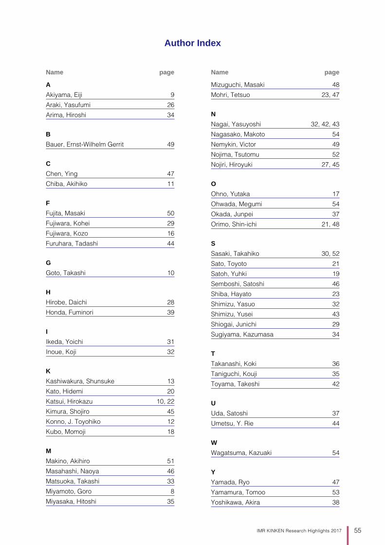
55IMR KINKEN Research Highlights 2017
A
Akiyama, Eiji 9
Araki, Yasufumi 26
Arima, Hiroshi 34
B
Bauer, Ernst-Wilhelm Gerrit 49
C
Chen, Ying 47
Chiba, Akihiko 11
F
Fujita, Masaki 50
Fujiwara, Kohei 29
Fujiwara, Kozo 16
Furuhara, Tadashi 44
G
Goto, Takashi 10
H
Hirobe, Daichi 28
Honda, Fuminori 39
I
Ikeda, Yoichi 31
Inoue, Koji 32
K
Kashiwakura, Shunsuke 13
Kato, Hidemi 20
Katsui, Hirokazu 10, 22
Kimura, Shojiro 45
Konno, J. Toyohiko 12
Kubo, Momoji 18
M
Makino, Akihiro 51
Masahashi, Naoya 46
Matsuoka, Takashi 33
Miyamoto, Goro 8
Miyasaka, Hitoshi 35
Mizuguchi, Masaki 48
Mohri, Tetsuo 23, 47
N
Nagai, Yasuyoshi 32, 42, 43
Nagasako, Makoto 54
Nemykin, Victor 49
Nojima, Tsutomu 52
Nojiri, Hiroyuki 27, 45
O
Ohno, Yutaka 17
Ohwada, Megumi 54
Okada, Junpei 37
Orimo, Shin-ichi 21, 48
S
Sasaki, Takahiko 30, 52
Sato, Toyoto 21
Satoh, Yuhki 19
Semboshi, Satoshi 46
Shiba, Hayato 23
Shimizu, Yasuo 32
Shimizu, Yusei 43
Shiogai, Junichi 29
Sugiyama, Kazumasa 34
T
Takanashi, Koki 36
Taniguchi, Kouji 35
Toyama, Takeshi 42
U
Uda, Satoshi 37
Umetsu, Y. Rie 44
W
Wagatsuma, Kazuaki 54
Y
Yamada, Ryo 47
Yamamura, Tomoo 53
Yoshikawa, Akira 38
Name page Name page
Author Index
56 IMR KINKEN Research Highlights 2017
A
age-hardening 12
alloy 11
amorphous 23, 37
atom probe tomography 32
aluminum alloys 12
C
ceramic 18
chemical vapor deposition (CVD) 10, 22
corrosion 9
crystal growth 16
D
deformation 11
domain wall 26
doping 35
E
electrical properties 30, 39
electron irradiation 19
electronic material 32
energy storage 21
eutectics 38
F
field-effect transistor 29
foam 20
G
grain boundaries 17
Goldschmidt tolerance factor 21
H
heavy fermion 31
high magnetic field 27
high pressure 39
high strength steel 9
hydride 21
I
ionic conductor 22
L
laser plasma 13
M
magnetic 28, 31
magnetic properties 35, 36
mechanical properties 23
metal-insulator transition 30
microstructure 10, 11, 22
molecular devices 35
molecular dynamics 18
N
nanostructure 20, 32
neutron scattering 27
nitride 33
nuclear materials 19
nucleation & growth 8
O
organic 30
oxide 29
P
parity symmetry breaking 31
phase transformation 8, 12
porosity 20
Q
quantum spin system 28
S
scintillator 38
simulation 18,19, 23
Si 37
sintering 10
solar cells 16,17
spectroscopy 13
spin dynamics 36
spintronics 26, 28
steel 8
structure 34
supercooled liquid 37
surface reaction 9
T
thin films 29, 33
tourmaline 34
V
valence transition 39
vapor phase epitaxy (VPE) 33
W
Weyl semimetal 26
X
XAFS 34
X-ray scattering 27
X-ray imaging 38
Keyword page Keyword page
Keyword Index

Editors Atsushi Tsukazaki, Gerrit E.W. Bauer, Kozo Fujiwara, Yusuke Nambu, Junpei Okada, and Shigeyuki Takagi
Editorial Staff Misa Yokoyama, Aki Oikawa, and Izumi Suda
Printing HOKUTO Corporation
Organization Institute for Materials Research Tohoku University 2-1-1 Katahira, Aoba-ku, Sendai 980-8577, Japan Tel. +81-(0)22-215-2144 Fax. +81-(0)22-215-2482
URL: http://www.imr.tohoku.ac.jp/E-mail: [email protected]
© IMR July 2017

2
0
1
72
0
1
72
0
1
72
0
1
7K
IN
KE
N
Re
se
ar
ch
H
ig
hl
ig
ht
s