
KGD 2012 - MEPTEC.ORG - Cadence.pdf · © IMEC/Cadence 2012 – KGD 2 1. Introduction and...
30
Sergej Deutsch 1 , Vivek Chickermane 2 , Brion Keller 2 , Bassilios Petrakis 3 , Erik Jan Marinissen 4 1 Duke, 2 Endicott, 3 San Jose 4 Leuven KGD 2012
Transcript of KGD 2012 - MEPTEC.ORG - Cadence.pdf · © IMEC/Cadence 2012 – KGD 2 1. Introduction and...

© IMEC 2011 / CONFIDENTIAL - Erik Jan Marinissen 1
Sergej Deutsch1, Vivek Chickermane2, Brion Keller2, Bassilios Petrakis3, Erik Jan Marinissen4
1Duke, 2Endicott, 3San Jose 4Leuven
KGD 2012

© IMEC/Cadence 2012 – KGD 2
1. Introduction and Background 2. 3D-DfT Requirements 3. 3D-DfT Architecture 4. Wrapper Generation Flow 5. Skin Model Generation 6. Results 7. Conclusion

© IMEC/Cadence 2012 – KGD 3
• IBM Thermal Conduction Modules
– MCMs with up to 121 Dies – Cap with heat removing pistons
TCM before Cap Applied
TCM with Thermal Cap
• Dies essentially had to be Good
– Chips Wafer tested to 99.9%+ – 1-(.999)120 → 12% defective
• Limited ability to remove/repair bad Die
– C4 Solder re-melted – Not always successful
• State of the Art early 1980’s
– ~1500 Watts Heat

© IMEC/Cadence 2012 – KGD 4
Direct Die-to-Die connection using TSVs
Allows stacking of Die on a module
There are Test impacts
Traditional 2D MCM Die Grid

© IMEC/Cadence 2012 – KGD 5
• 3D chip stacking with wire-bonds
– Heterogeneous technologies – Dense integration, small footprint
board
board
System-in-Package (SiP)
TSV-Based 3D-SIC
• Through-Silicon Vias (TSVs): Metal vias that provide interconnects from front-side to back-side through silicon substrate
• TSV benefits
– Even more dense integration – High density, low capacitance – Increased bandwidth – Increased performance – Lower power dissipation – Lower manufacturing cost?

© IMEC/Cadence 2012 – KGD 6
• Potential test moments
1. Pre-Bond Test : before stacking 2. Mid-Bond Test : partial stack 3. Post-Bond Test : full stack 4. Final Test : after packaging
3D-SIC
wafer fab 2
Pre-Bond Test 2
assembly & packaging
Final Test
wafer fab 3
Pre-Bond Test 3
wafer fab 1
Pre-Bond Test 1
stacking 1+2
Mid-Bond Test 1+2
stacking (1+2)+3
Post-Bond Test 1+2+3
• Not all tests are mandatory always! − Cost/benefit modeling to determine
most cost-efficient test flow • Wafer cost, die size, die yield • Stacking approach (W2W vs. D2W/D2D),
stacking yield • Test coverage, test cost • Package cost
[Taouil et al. – ATS’10]

© IMEC/Cadence 2012 – KGD 7
• Probe pitch (today, scaling down)
– Micro-bumps : ∅ 25µm, pitch 40µm – Direct TSV connects : ∅ 5µm, pitch 10µm
face
carrier wafer
face
• Array size − 1,000 to 10,000+ TSVs to probe
• How to verify die is fully functional? − Cannot touch all TSV I/Os − Upper die only have micro-bumps − No standard functional pads
• Keys for die testing: − Use reduced pin testing approach − Add wafer-test-only pads as needed − Use I/O Wrap to test pins not contacted

© IMEC/Cadence 2012 – KGD 8
• Pre-Bond Test
– Original thick or thinned-down wafer – Probe access at DUT – Probe on micro-bumps or dedicated pads – Assuming TSVs not contacted – use I/O Wrap Test
die
• Mid-Bond / Post-Bond / Final Tests
– Test access (probe or socket) thru bottom die – Require DfT to propagate test data
up/down through stack – Requirements
– Modular test: core, die, interconnect – TestTurn: test up till this die – TestElevator: test higher-up die
– Inter-chip communication paths (TSVs) fully tested here
bottom die
middle die
top die

© IMEC/Cadence 2012 – KGD 9
Board
Die 1
Die 2
Die 3
Core 3
Core 2.1
Core 1.1 Core 1.2 Core 1.3
Core 2.2
TSV
TSV
TSV
TSV
TSV
TSV
TSV
TSV
TSV
TSV
TSV
TSV
TSV
TSV
TSV
TSV
pin pin pin pin
Functional Design • ≥2 stacked dies, possibly core-based • Inter-connect: TSVs • Extra-connect: pins
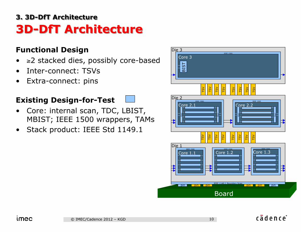
© IMEC/Cadence 2012 – KGD 10
Board
Die 1
Die 2
Die 3
Core 3
Core 2.1
Core 1.1 Core 1.2 Core 1.3
Core 2.2
BIS
T
TD
C
TD
C
TD
C
TD
C
IEEE 1149.1 Boundary Scan
IEEE 1500 IEEE 1500 IEEE 1500
IEEE 1500
IEEE 1500
IEEE 1500
TSV
TSV
TSV
TSV
TSV
TSV
TSV
TSV
TSV
TSV
TSV
TSV
TSV
TSV
TSV
TSV
pin pin pin pin pin pin
Functional Design • ≥2 stacked dies, possibly core-based • Inter-connect: TSVs • Extra-connect: pins
Existing Design-for-Test • Core: internal scan, TDC, LBIST,
MBIST; IEEE 1500 wrappers, TAMs • Stack product: IEEE Std 1149.1
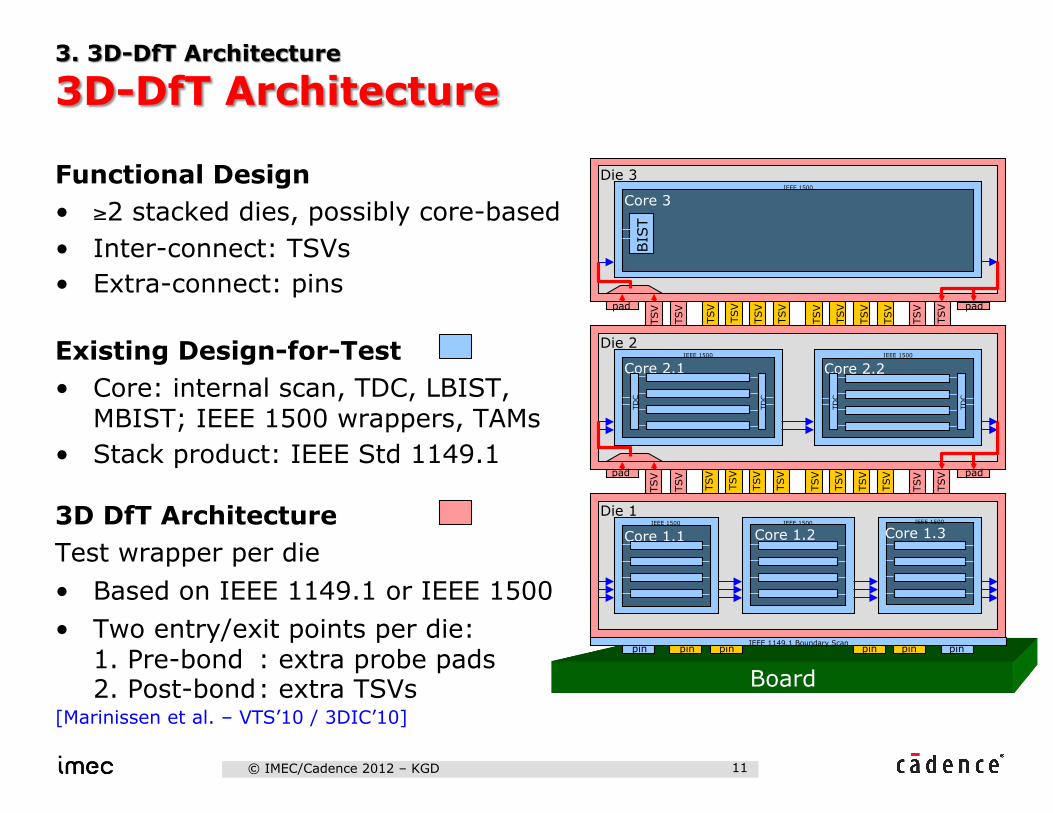
© IMEC/Cadence 2012 – KGD 11
Board
Die 1
Die 2
Die 3
Core 3
Core 2.1
Core 1.1 Core 1.2 Core 1.3
Core 2.2
BIS
T
TD
C
TD
C
TD
C
TD
C
IEEE 1149.1 Boundary Scan
IEEE 1500 IEEE 1500 IEEE 1500
IEEE 1500
IEEE 1500
IEEE 1500
TSV
TSV
TSV
TSV
TSV
TSV
TSV
TSV
TSV
TSV
TSV
TSV
TSV
TSV
TSV
TSV
pin pin pin pin pin pin
TSV
TSV
TSV
TSV
TSV
TSV
TSV
TSV pad
pad
pad
pad
Functional Design • ≥2 stacked dies, possibly core-based • Inter-connect: TSVs • Extra-connect: pins
Existing Design-for-Test • Core: internal scan, TDC, LBIST,
MBIST; IEEE 1500 wrappers, TAMs • Stack product: IEEE Std 1149.1
3D DfT Architecture Test wrapper per die • Based on IEEE 1149.1 or IEEE 1500 • Two entry/exit points per die:
1. Pre-bond : extra probe pads 2. Post-bond : extra TSVs
[Marinissen et al. – VTS’10 / 3DIC’10]

© IMEC/Cadence 2012 – KGD 12
• Conventional (2D) IEEE 1500 Features
– Wrapper Serial Control (WSC): WRCK, WRSTN, SelectWIR, ShiftWR, CaptureWR, UpdateWR, TransferDR*
– Serial interface: WSI-WSO – Parallel interface: WPI*-WPO* – Wrapper Instruction Register (WIR) – Wrapper Boundary Register (WBR) – Serial and parallel* Bypass
* = optional
Core x
WIR
scan chain
WBR
scan chain
bypass
bypass switch
box
switch
box
n
WSI
WSC
WSO
WPI* WPO* n
1
6
1
Note: Figure abstracts from functional circuitry and only shows DfT features

© IMEC/Cadence 2012 – KGD 13
• New 3D Features
1. TestTurns • Serial and parallel interface
towards bottom die • Flip-flops for clean timing
2. Probe pads on non-bottom dies • Mandatory on WSC, WSI-WSO • Scalable on WPI-WPO
4. Hierarchical bypass for higher-level dies and/or embedded cores (not shown here)
3. TestElevators to higher-up die(s) • Mirrored standard 1500 interface: WSCs, WSIs-WSOs, WPIs-WPOs
Die x
WIR
scan chain
WBR
scan chain
bypass
bypass switch
box
switch
box
n
WSI
WSC
WSO
n
1
6
1
WPI* WPO*
Die x
WIR
scan chain
WBR
scan chain
bypass
bypass switch
box
switch
box
to/fro
m b
otto
m d
ie WSI
WSC
WSO
n
1
6
1
n
WPI*
WPO*
m
m
to/fro
m to
p d
ie
WSOs
WSCs
WSIs
WPOs
WPIs
n
1
6
1
n
[Marinissen et al. – VTS’10]
Note: Figure abstracts from functional circuitry and only shows DfT features

© IMEC/Cadence 2012 – KGD 14
Note: Figure abstracts from functional circuitry and only shows DfT features
ParallelPostbond BypassElevator
Die 2
WSI
WSC
WIR2
WSO
scan chain
WBR
scan chain
bypass
bypass
WPI*
WPO*
switch
box
Die 3 (top)
WIR3
scan chain
WBR
scan chain
switch
box
bypass
bypass switch
box
Die 1 (bottom)
TDI
WIR1
scan chain
WBR
scan chain
switch
box
bypass
bypass switch
box
1149.1
TCK
TMS
TRSTN*
TDO
WPI*
WPO*
switch
box
n
1
6
1
n
WSI
WSC
WSO
WPI*
WPO*
n
1
6
1
n
WIR2 WIR3 WIR1
1149.1
scan chain
WBR
scan chain
bypass
ParallelPostbond IntestTurn
ParallelPostbond BypassTurn

© IMEC/Cadence 2012 – KGD 15
Note: Figure abstracts from functional circuitry and only shows DfT features
ParallelPostbond BypassElevator
WSI
WSC
WSO
WPI*
WPO*
Die 2 (middle)
scan chain
WBR
scan chain
switch
box
bypass
bypass switch
box
Die 1 (bottom)
TDI
WIR1
scan chain
WBR
scan chain
switch
box
bypass
bypass switch
box
1149.1
TCK
TMS
TRSTN*
TDO
WPI*
WPO*
n
1
6
1
n
ParallelPostbond BypassTurn
DRAM 1...n (top)
Boundary R
egs
WIR2 DRAM Ctrl
I/O D
rivers/Receivers
Wide-IO DRAM (JEDEC Standard)
Memory Stacking will Drive 3D

© IMEC/Cadence 2012 – KGD 16
Die 1
bypass
WSI
WSC
WSO
n
1
6
1
n
WPI*
WPO*
bypass
WIR
Wra
pp
er B
ou
nd
ary
Reg
ister
Wra
pp
er B
ou
nd
ary
Reg
ister
scan chain
switch
box
switch
box
scan chain
Die N
bypass
WSI
WSC
WSO
n
1
6
1
n
WPI*
WPO*
m
bypass
WIR
m
Wra
pp
er B
ou
nd
ary
Reg
ister
scan chain
switch
box
switch
box
scan chain
Bo
un
dary
Sca
n R
eg
ister
switch
box
TDI
TCK
TMS
TRSTN*
TDO
Adap
ter
1149.1
WSIs
WPIs
n
1
6
1
n
Functio
nal I/O
s / WPI/W
PO

© IMEC/Cadence 2012 – KGD 17

© IMEC/Cadence 2012 – KGD 18
J1500 wrapper cells
JTAG boundary cells
Logic Die
3D wrapper (1500)
SII
PAD
C I
PIN
J
OE
PAD
C I
PIN
J
w
OE
PAD
C I
PIN
J J
ww
w
Toward othe
r dies
w
OE
PAD
C I
PIN
JJ
w w
Input Output Tristateable output
Bidir
w
OE
w w w w w ww w

© IMEC/Cadence 2012 – KGD 19
DRAM (Die 1) Logic Die
DRAM (Die 2)
DRAM (Die 3)
DRAM (Die 4)

© IMEC/Cadence 2012 – KGD 20
DRAM Stack (up to 4 Dies)

© IMEC/Cadence 2012 – KGD 21
Design
Library
Wrapped Design
WIR Insertion
Wrapper Cell Insertion
Multimode Scan Chain Configuration
JTAG Insertion
User-defined Parameters
Bypass Register Insertion
3D Wrapper Insertion
JTAG Insertion
TAP Controller Insertion
Boundary Cell Insertion
WSC Signal Generation
DfT Insertion with Encounter RTL Compiler Wrapper Insertion
I/O Wrap Options
DRAM Control Options
Serial/Parallel Options

© IMEC/Cadence 2012 – KGD 22
Design
Library
Wrapped Design
WIR Insertion
Wrapper Cell Insertion
Multi-Mode Scan Chain Configuration
JTAG Insertion
User-defined Parameters
Bypass Register Insertion
3D Wrapper Insertion (RC)
JTAG Insertion
TAP Controller Insertion
Boundary Cell Insertion
JTAG-to-1500 WPOs
WPIs
WSOs
WSIs WSO
w
w
w
w
w
w
w
w
w
w
w
w
WIR
tow
ard
/fr
om
to
p d
ie
WSI
WPI
WSC
WPO
BPO[0]
BPO[1]
OEN
BPI[0]
BPI[1]
BPI[2] to
ward
/fr
om
exte
rnal I/
Os
scan chains
TDI
TDO
TMS
TCK
TRST JTAG Macro
• JTAG Macro insertion (TAP Controller, IR, decode logic)
• Boundary cell insertion at bottom I/Os
• JTAG-to-1500 (preventing pins)
– Operation sequence 1a. JTAG: “WIR Program” 1b. 1500: WIR Loading 2a. JTAG: “Scan” 2b. 1500: Scan
– Requires JTAG-to-1500 adapter
J
J
J
J
J
J
JTAG-to-1500

© IMEC/Cadence 2012 – KGD 23
internal scan
chains
internal scan
chains
in w
rap
per ce
lls
ou
t wra
pp
er ce
lls
in w
rap
per ce
lls
ou
t wra
pp
er ce
lls
turn
p
ar.
tu
rn
WSO
WSO_pad
WSI_pad
WSI
WSOs
WSIs
WPO
WPO_pad
WPI_pad
WPI WPOs
WPIs
Elevator/ Turn
Scan/Bypass Intest/Extest Prebond/ Postbond
Select WIR
Elevator/ Turn
Scan/Bypass Intest/Extest Prebond/ Postbond
WB
Y
par. b
yp
asse
s
• Skin Model includes
– Boundary Scan Chains – Wrapper Cells – Control Registers (WIR) – Includes logic to run all
EXTEST instructions/Modes – Serial and Parallel versions
• Intent is to exclude – Internal Scan Chains – Internal Logic
• Skin Model – Normally <5% of chip – Used in higher-level
package test
Serial
Parallel
WIR shift register

© IMEC/Cadence 2012 – KGD 24
Traditional 2D MCM Die Grid or with new 3D Stacking
• Stacked Skin Models can be less than one chip’s logic • Extest and Bypass modes work directly • Enables − Interconnect Test Generation − Test Migration

© IMEC/Cadence 2012 – KGD 25
Encounter RTL Compiler 3D-DfT Wrapper Insertion
Physical Design + Verification
Pre-Bond Test
Wafer Fab
Encounter Test DfT Rule Check
netlist
netlist
Pattern Simulation
patterns
skin model pre-tested die
layout
die
patterns
Encounter Test Skin-Model Gen.
Encounter Test Migration Prep
Encounter Test ATPG
Functional Design + Verification

© IMEC/Cadence 2012 – KGD 26
Encounter Test Intest Migration
Stacking Encounter Test Intest Migration
die1 dien
Encounter Test Interconnect-ATPG
pat1 patn sm1 smn
Test Scheduling
intest1...n extest
Mid-Bond/Post-Bond/Final Test
stack
stack test
tested stack
Stack Design + Verification
Pattern Simulation
stack netlist
... ... ...
Encounter RC Add Test Connects
stack netlist

© IMEC/Cadence 2012 – KGD 27
First test chip • 65nm CMOS • Functional design
– 727 functional I/Os – 229,249 std. cells – 28,224 flip-flops – Area 2,070,536µm2
• Skin Model – ~1,000 flops – ~3.5%
DfT Item Δ Area Scan Chains +7.8% 3D Wrapper +1.0% JTAG Wrapper +0.6%
Simple test cases:

© IMEC/Cadence 2012 – KGD 28
• Test case with 2 Logic Die and WideIO DRAM
• WideIO DRAM implementation does not support I/O Wrap! – Receiver path is blocked when Driver is enabled
• Otherwise all interconnects tested in stack – Logic-Logic and Logic-DRAM – All driver-to-receiver pairings tested (where not blocked) – 6 Test patterns covered ~2000 TSVs and their driver/receivers – Plus 20 tests for shorts between TSV signals and other chip I/O
• I/O Wrap is reasonable approach to test non-contacted I/Os – Many years of use for reduced-pin Testing

© IMEC/Cadence 2012 – KGD 29
• 3D chip stacking using Through-Silicon Vias has much potential
• 3D test challenges include pre-bond (KGD) and post-bond testing
• 3D-DfT Architecture – I/O Wrap & test-only pads for pre-bond testing – Serial and Parallel test access mechanisms – TestTurns: to bypass upper dies in stack – TestElevator mode: for test paths to/from upper dies – WideIO DRAM Top Control Interface
• 3D wrapper insertion flow – Inserts 1500-style wrappers and 1149.1 for bottom die – Includes controls for I/O Wrap and WideIO DRAM testing – Generates input to run ATPG
• Industrial case study: low area cost and small package skin model

KGD
Thank You!


![INVENTIVE - Si2projects.si2.org/events_dir/2007/date/cadence.pdf · INVENTIVE Common Power Format: ... ATPG Constraint Validation Equivalence checking ... [ -sdc_files sdc_file_list]](https://static.fdocuments.us/doc/165x107/5ac901cf7f8b9aa3298c99f7/inventive-common-power-format-atpg-constraint-validation-equivalence-checking.jpg)
![KGD-600 installation guideR]070402.pdf · -1-KGD-600 Industrial Web Smart 6-Port Gigabit Ethernet Switch with Fiber Connectivity Installation Guide DOC.070402](https://static.fdocuments.us/doc/165x107/5ec11a9b8a61273589574a42/kgd-600-installation-r070402pdf-1-kgd-600-industrial-web-smart-6-port-gigabit.jpg)