KEELOQ HCS30X, HCX200 Stand-Alone Programmerww1.microchip.com/downloads/en/AppNotes/00217a.pdf ·...
24
2001 Microchip Technology Inc. DS00217A-page 1 AN217 OVERVIEW This application note describes how to implement a KEELOQ stand-alone programmer using a Microchip PIC16F84A microcontroller. The PIC16F84A is a FLASH microcontroller with 64 bytes of internal EEPROM that, in this design, is used to store the incremental serial number programmed into HCS encoders every time. All the other HCS con- figuration parameters are defined as constants in the FLASH program memory of the PIC16F84A. Two learning schemes are implemented: • The simple learning scheme for which you can find the complete software in this application note. • The normal learning scheme with the applicable software included in the KEELOQ license agree- ment disks (this software includes the KEELOQ decryption routine). In the first scheme, the Encryption Key programmed in the HCS encoders is always the same and equal to the Manufacturer's Code. In the second scheme, before starting to program the encoder, the PIC16F84A calculates the Encryption Key for that encoder using the 64-bit Manufacturer's Code and the 28-bit serial number running the KEELOQ decryption algorithm. FIGURE 1: PIC16F84A PIN OUT KEELOQ SIMPLE LEARNING SCHEME (Fixed Key) This learning scheme implements the lowest level of security for a KEELOQ based security system. With this method, every programmed encoder has a different serial number, but the same fixed Encryption Key is equal to the chosen Manufacturer's Code. FIGURE 2: SIMPLE LEARNING SCHEME An explanation of the different security levels can be found in the "Secure Data Products Handbook" (Com- parison Chart, Section 1 [DS40168]). The application note AN659 (KEELOQ Simple Code Hopping Decode [DS00663]), implements a decoder that can be used with an encoder using the simple learning method. KEELOQ NORMAL LEARNING SCHEME (Serial Number Derived System) In this case, every transmitter is programmed with an incremental unique serial number. This serial number is used in conjunction with the 64-bit Manufacturer's Code and the KEELOQ algorithm to generate the Encryption Key. This Encryption Key is programmed into the encoder, thus, every transmitter has a different key that is used to encrypt the data. A detailed explanation of this learning scheme can be found in the Technical Brief TB001 [DS91000A], part of the Microchip Secure Data Products Handbook. The application note AN642 (KEELOQ Code Hopping Decoder Using a PIC16C56, [DS00642]), implements a decoder that can be used with the HCS programmed in this normal method. Notice: This is a non-restricted version of Application Note AN218 which is available under the KEELOQ License Agreement. The license agreement can be ordered from the Microchip Literature Center as DS40149. Author: Maurizio Fiammeni Microchip Technology Inc. PDIP, SOIC RA1 RA0 OSC2/CLKOUT VDD RB6 RB5 RB4 OSC1/CLKIN RA2 RA3 MCLR VSS RB0/INT RB1 RB2 RB3 RA4/T0CKI RB7 2 3 4 5 6 7 8 9 •1 17 16 14 13 12 11 10 15 18 PIC16F84A 13 64-bit Manufacturer’s Code Encryption Key KEELOQ ® HCS30X, HCS200 Stand-Alone Programmer
Transcript of KEELOQ HCS30X, HCX200 Stand-Alone Programmerww1.microchip.com/downloads/en/AppNotes/00217a.pdf ·...

AN217KEELOQ® HCS30X, HCS200 Stand-Alone Programmer
OVERVIEW
This application note describes how to implement aKEELOQ stand-alone programmer using a MicrochipPIC16F84A microcontroller.
The PIC16F84A is a FLASH microcontroller with 64bytes of internal EEPROM that, in this design, is usedto store the incremental serial number programmedinto HCS encoders every time. All the other HCS con-figuration parameters are defined as constants in theFLASH program memory of the PIC16F84A.
Two learning schemes are implemented:
• The simple learning scheme for which you can find the complete software in this application note.
• The normal learning scheme with the applicable software included in the KEELOQ license agree-ment disks (this software includes the KEELOQ decryption routine).
In the first scheme, the Encryption Key programmed inthe HCS encoders is always the same and equal to theManufacturer's Code.
In the second scheme, before starting to program theencoder, the PIC16F84A calculates the Encryption Keyfor that encoder using the 64-bit Manufacturer's Codeand the 28-bit serial number running the KEELOQ
decryption algorithm.
FIGURE 1: PIC16F84A PIN OUT
KEELOQ SIMPLE LEARNING SCHEME
(Fixed Key)
This learning scheme implements the lowest level ofsecurity for a KEELOQ based security system. With thismethod, every programmed encoder has a differentserial number, but the same fixed Encryption Key isequal to the chosen Manufacturer's Code.
FIGURE 2: SIMPLE LEARNING SCHEME
An explanation of the different security levels can befound in the "Secure Data Products Handbook" (Com-parison Chart, Section 1 [DS40168]).
The application note AN659 (KEELOQ Simple CodeHopping Decode [DS00663]), implements a decoderthat can be used with an encoder using the simplelearning method.
KEELOQ NORMAL LEARNING SCHEME
(Serial Number Derived System)
In this case, every transmitter is programmed with anincremental unique serial number. This serial number isused in conjunction with the 64-bit Manufacturer'sCode and the KEELOQ algorithm to generate theEncryption Key. This Encryption Key is programmedinto the encoder, thus, every transmitter has a differentkey that is used to encrypt the data.
A detailed explanation of this learning scheme can befound in the Technical Brief TB001 [DS91000A], part ofthe Microchip Secure Data Products Handbook.
The application note AN642 (KEELOQ Code HoppingDecoder Using a PIC16C56, [DS00642]), implements adecoder that can be used with the HCS programmed inthis normal method.
Notice:
This is a non-restricted version of Application Note AN218 which is available under the KEELOQ License Agreement. The license agreement can be ordered from the Microchip Literature Center as DS40149.
Author: Maurizio FiammeniMicrochip Technology Inc.
PDIP, SOIC
RA1RA0
OSC2/CLKOUTVDD
RB6RB5RB4
OSC1/CLKIN
RA2RA3
MCLRVSS
RB0/INTRB1RB2RB3
RA4/T0CKI
RB7
2 3 4 5 6 7 8 9
•11716
1413121110
15
18
PIC
16F84A
13
64-bitManufacturer’s Code Encryption Key
2001 Microchip Technology Inc. DS00217A-page 1

AN217
The key generation scheme is shown below:
FIGURE 3: NORMAL (SERIAL NUMBER-DERIVED) LEARNING SCHEME
OTHER POSSIBLE LEARNING SCHEMES
(Secure Seed-Derived System)
The two learning methods implemented in this applica-tion note are not the only schemes applicable. Refer toTechnical Brief TB001 for more information on SecureLearning schemes.
Furthermore, custom learning scheme solutions canalso be implemented.
ENCODER EEPROM MEMORY ORGANIZATION
The KEELOQ encoders are EEPROM based deviceswith a built-in oscillator, wake-up on button press, resetcircuit and internal logic state machine (Figure 4).
FIGURE 4: HCS300 BLOCK DIAGRAM
The HCS200, HCS300 and HCS301 contain 192 bits(12 * 16-bit words) of EEPROM memory (Table 1). ThisEEPROM array is used to store the Encryption Key, thesynchronization value, the serial number, etc.
A detailed description of the memory map is repre-sented in Table 1.
02H+SN
Transformation(Decrypt or XOR)
64-bit Manufacturer’sCode
Upper 32 bits of key
06H+SN
Transformation(Decrypt or XOR)
64-bit Manufacturer’sCode
Lower 32 bits of key
Controller
PowerLatching
andSwitching
Oscillator
Reset Circuit
LED Driver
EEPROM Encoder
32-bit Shift Register
Button Input PortVSS
VDD
PWM
LED
S3 S2 S1 S0
DS00217A-page 2 2001 Microchip Technology Inc.

AN217
TABLE 1: HCS30X EEPROM MEMORY MAP
Note: The MSb of the serial number contains abit used to select the auto shut-off timer.
In order to create the encrypted message transmittedto the receiver, the encoder uses the 64-bit EncryptionKey and the 16-bit synchronous counter.
Certain configuration options can be selected for thedifferent encoders. Table 2 shows the configurationword for the HCS300/1.
TABLE 2: HCS30X CONFIGURATION WORD
Note: Please refer to the HCS200 data sheet[DS40138] for configuration details.
WORDADDRESS
MNEMONIC DESCRIPTION
0 KEY_0 64-bit Encryption Key(word 0)
1 KEY_1 64-bit Encryption Key(word 1)
2 KEY_2 64-bit Encryption Key(word 2)
3 KEY_3 64-bit Encryption Key(word 3)
4 SYNC 16-bit SynchronizationValue
5 RESERVED Set to 0000H
6 SER_0 Device Serial Number(word 0)
7 SER_1 Device Serial Number(word 1)
8 SEED_0 Seed Value (word 0)
9 SEED_1 Seed Value (word 1)
10 EN_KEY 16-bit Envelope Key
11 CONFIG Config Word
BIT NUMBER BIT DESCRIPTION
0 Discrimination Bit 0
1 Discrimination Bit 1
2 Discrimination Bit 2
3 Discrimination Bit 3
4 Discrimination Bit 4
5 Discrimination Bit 5
6 Discrimination Bit 6
7 Discrimination Bit 7
8 Discrimination Bit 8
9 Discrimination Bit 9
10 Overflow bit 0 (OVR0)
11 Overflow bit 1 (OVR1)
12 Low Voltage Trip Point Select
13 Baud Rate Select Bit 0 (BSL0)
14 Baud Rate Select Bit 1 (BSL1)
15 Envelope Encryption Select (EENC)
2001 Microchip Technology Inc. DS00217A-page 3

AN217
PROGRAMMING/VERIFY WAVEFORM
The programming cycle allows programming of the192-bits representing the serial number, the EncryptionKey, the configuration word, etc., in a serial data streaminto the encoder EEPROM.
Programming is initiated by forcing the PWM line high,after the S2 line has been held high for the appropriatelength of time (TPS).
After the program mode is entered, a delay must beallowed during which the device erases the entirememory. This writes all locations in the EEPROM tozeros. The device can then be programmed by clockingin 16 bits at a time, using S2 as the clock line and PWM
as the data in line. After each 16-bit word is loaded, aprogramming delay is required for the internal programcycle to complete. This delay can take up to TWC (seeTable 3).
At the end of the programming cycle, the device can beverified (Figure 6) by reading back the EEPROM.Clocking the S2 line reads back the data on the PWMline. For security reasons, it is not possible to executea verify function without first programming theEEPROM.
A verify operation can only be done once, immediatelyfollowing the program cycle. This is important to pre-vent reading the internal memory of the encoder onceit has been programmed.
FIGURE 5: PROGRAMMING WAVEFORMS
FIGURE 6: VERIFY WAVEFORMS
Note: For the HCS300 and HCS301, both the S2 pin and the S3 pin can be used as programming clock lines, andfor the HCS200, only the S2 pin can be the clock line.
Enter ProgramMode TPBW
TCLKH TDS
TCLKL TDH
TWC
TPS TPH1
TPH2 Data for Word 0 (Key 0) Data for Word 1
Repeat 12 times for each word
S3(Clock)
PWM(Data) Bit 0 Bit 1 Bit 2 Bit 3 Bit 14 Bit 15 Bit 16 Bit 17
Note 1: Unused button inputs to be held to ground during the entire programming sequence.2: The VDD pin must be taken to ground after a program/verify cycle.
Repeat 12 times for each word
End ofProgramming Cycle
Begin Verify Cycle HereData in Word 0
TWC TDV
PWM(Data)
S3(Clock)
Note: If a Verify operation is to be done, then it must immediately follow the Program cycle.
Bit190 Bit191 Bit 0 Bit 1 Bit 2 Bit 3 Bit 14 Bit 15 Bit 16 Bit 17 Bit190 Bit191
DS00217A-page 4 2001 Microchip Technology Inc.

AN217
TABLE 3: PROGRAMMING/VERIFY TIMING REQUIREMENTS
VDD = 5.0V ± 10%25°C ± 5°C
Parameter Symbol Min. Max. Units
Program Mode Setup Time TPS 3.5 4.5 ms
Hold Time 1 TPH1 3.5 — ms
Hold Time 2 TPH2 50 — µs
Bulk Write Time TPBW — 2.2 ms
Program Delay Time TPROG — 2.2 ms
Program Cycle Time TWC — 36 ms
Clock Low Time TCLKL 25 — µs
Clock High Time TCLKH 25 — µs
Data Setup Time TDS 0 — µs
Data Hold Time TDH 18 — µs
Data Out Valid Time TDV 10 24 µs
2001 Microchip Technology Inc. DS00217A-page 5

AN217
SOFTWARE IMPLEMENTATION
The software that implements the encoder programmerruns on the PIC16F84A.
The 64-bit Manufacturer’s Code is stored in the internalPIC16F84A FLASH memory. This cannot be read if thedevice is code protected.
All the other parameters in the configuration word of theencoder are in the FLASH program memory of thePIC16F84A, where they are defined as constants.
The serial number programmed every time into theencoder is located instead, in the internal EEPROMdata memory of the PIC16F84A.
In order to change the Manufacturer Code (MKEY_X),or some parameter of the configuration word, as thevoltage selection (VLOW), the baud rates transmission(BSL0, BSL1), etc., a change in the firmware isrequired. The following define can be modified in theassembly code:
===========================================================================================MODIFYABLE PROGRAMMING DEFINE===========================================================================================
#DEFINE KEY_METHOD 1 ; MUST BE 1 IF NORMAL KEY GEN METHOD TO BE USED; MUST BE 0 IF SIMPLE KEY GEN METHOD TO BE USED; (ENCRYPTION KEY= MANUFACTURER KEY)
#DEFINE HCS30X 1 ; MUST BE 1 IF PROGRAMMING HCS300-301,; MUST BE 0 IF PROGRAMMING HCS200
#DEFINE MCODE_0 0xCDEF ; LSWORD#DEFINE MCODE_1 0x89AB#DEFINE MCODE_2 0x4567#DEFINE MCODE_3 0x0123 ; MSWORD
#DEFINE SYNC 0X0000 ; SYNCRONOUS COUNTER
#DEFINE SEED_0 0x0000 ; 2 WORD SEED VALUE#DEFINE SEED_1 0x0000
#DEFINE ENV_KEY 0x0000 ; ENVELOPE KEY (NOT USED FOR HCS200)
#DEFINE AUTOFF 1 ; AUTO SHUT OFF TIMER ( NOT USED FOR HCS200)
#DEFINE DISC70 0x00 ; DISCRIMINATION BIT7-BIT0#DEFINE DISC8 0 ; DISCRIMINATION BIT8#DEFINE DISC9 0 ; DISCRIMINATION BIT9#DEFINE OVR0 0 ; OVERFLOW BIT0 (DISC10 for HCS200)#DEFINE OVR1 0 ; OVERFLOW BIT1(DISC11 for HCS200)#DEFINE VLOW 1 ; LOW VOLTAGE TRIP POINT SELECT BIT (1=High voltage)#DEFINE BSL0 0 ; BAUD RATE SELECT BIT0#DEFINE BSL1 0 ; BAUD RATE SELECT BIT1(RESERVED for HCS200)#DEFINE EENC 0 ; ENVELOPE ENCRYPTION SELECT(RESERVED for
; HCS200)
#DEFINE DISEQSN 1 ; IF DISEQSN=1 SET DISCRIMINANT EQUAL TO; SERNUM BIT10-0 IF DISEQSN=0 SET DISCRIMINANT; AS DEFINED ABOVE
===========================================================================================
Note: The PIC16F84A program to build the HCS EEPROM memory map uses all these parameters.
DS00217A-page 6 2001 Microchip Technology Inc.

AN217
The software given with this application note imple-ments the Simple Key generation method, while thesoftware that implements the Normal Key method iscontained in the KEELOQ License agreement disks.
The software is composed of four main functions:
• Main loop routines• Encryption Key generation routines
• Programming HCS routines• Verify HCS routines
Main Loop Routine (M_KEY_GEN: SIMPLE_KEY_GEN, NORMAL_KEY_GEN, MAP_SET)
The program simply waits for a button press to proceedto the programming routines.
Encryption Routines (M_KEY_GEN: SIMPLE_KEY_GEN, NORMAL_KEY_GEN, MAP_SET)
The M_KEY_GEN routine can be different, by justchanging the parameter called KEY_METHOD from 0 to1 in the modifiable table.
With the Simple Key generation method, theSIMPLE_KEY_GEN routine sets the Encryption Keyequal to the Manufacturer Code. TheNORMAL_KEY_GEN routine uses the KEELOQ decryp-tion algorithm in order to create the Encryption Key,starting from the Manufacturer Code and the currentserial number read from the PIC16F84A internal datamemory.
The MAP_SET routine prepares the 12 words (WORD0- WORD11) to be programmed in the HCS EEPROMmap.
Programming HCS Routines (M_PROGRAMMING)
This routine starts driving the PWM line high, after theS2 line has been held high for the appropriate length oftime, in order to bulk erase the encoder after 2.2 ms(TPBW).
Then, the M_NEW_WORD routine outputs the first word tobe programmed on the PWM line synchronously withthe clock S2 line and waits for the 36 ms of program-ming time (TWC).
This routine is repeated 12 times completing the entireprogramming of the HCS EEPROM memory map.
The WAIT_uS and WAIT_WMSEC implements softwaredelay routines to wait micro or milliseconds.
Verify HCS Routines (M_VERIFY)
At the end of the 12th word programmed, theM_VERIFY routine continues to drive the clock line S2,reading back the EEPROM memory and verifying whatwas programmed before.
If the verify is right, it is indicated by 0.4 seconds LEDon (PROG_SUCCESS). If not, the LED will blink for 4 sec-onds (PROG_ERR) before going back to the M_LOOP.
For further analysis, consult the following literature:
KEELOQ Code Hopping Decoder on a PIC16C56
AN642 DS00642
Converting NTQ105/106 Designs to HCS200/300s
AN644 DS00644
Code Hopping Security System on a PIC16C57
AN645 DS00645
Secure Learn Code Hopping Decoder on a PIC16C56
AN652 DS00652
KEELOQ Simple Code Hopping Decoder
AN659 DS00659
KEELOQ Code Hopping Decoder on a PIC16C56 (public version)
AN661 DS00661
Secure Learn Code Hopping Decoder on a PIC16C56 (public version)
AN662 DS00662
KEELOQ Simple Code Hopping Decoder (public version)
AN663 DS00663
Using KEELOQ to Generate Hopping Passwords
AN665 DS00665
PICmicro Mid-Range MCU Code Hopping Decoder
AN662 DS00672
HCS410 Transponder Decoder using a PIC16C56
AN675 DS00675
Modular PICmicro Mid-Range MCU Code Hopping Decoder
AN742 DS00742
Modular Mid-Range PICmicro KEELOQ Decoder in C
AN744 DS00744
Secure Learning RKE Systems Using KEELOQ Encoders
TB001 DS91000
An Introduction to KEELOQ Code Hopping
TB003 DS91002
A Guide to Designing for EuroHomelink Compatibility
TB021 DS91021
KEELOQ Decryption & IFF Algorithms
TB030 DS91030
KEELOQ Decryption Routines in C
TB041 DS91041
Interfacing a KEELOQ Encoder to a PLL Circuit
TB042 DS91042
KEELOQ CRC Verification Routines
TB043 DS91043
2001 Microchip Technology Inc. DS00217A-page 7

AN217
FIGURE 7: PROGRAMMING FLOW DIAGRAM
ResetRESET_VECTOR
Initialize Ports,Register and RAM
START
NO
YES
Read and incrementserial number from
EEPROMREAD_SN
Key generation:KEY_GEN
(Simple or Normalmethod)
Load words to beprogrammed into HCS
memory mapMAP_SET
HCS programmingM_PROGRAMMING
YES NO
M_VERIFY
LED on for 0,4 secWrite SN programmed
into EEPROMPROG_SUCCES
Programming error4 sec LED blinking
PROG_ERR
Button released?M_END
Program buttonpressed?M_LOOP
HCS verify ok?
YESNO
DS00217A-page 8 2001 Microchip Technology Inc.
AN217
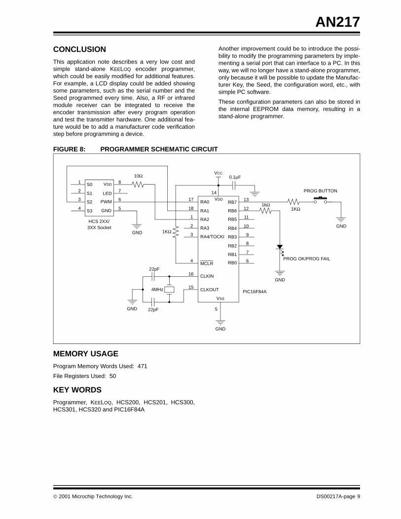
CONCLUSION
This application note describes a very low cost andsimple stand-alone KEELOQ encoder programmer,which could be easily modified for additional features.For example, a LCD display could be added showingsome parameters, such as the serial number and theSeed programmed every time. Also, a RF or infraredmodule receiver can be integrated to receive theencoder transmission after every program operationand test the transmitter hardware. One additional fea-ture would be to add a manufacturer code verificationstep before programming a device.
Another improvement could be to introduce the possi-bility to modify the programming parameters by imple-menting a serial port that can interface to a PC. In thisway, we will no longer have a stand-alone programmer,only because it will be possible to update the Manufac-turer Key, the Seed, the configuration word, etc., withsimple PC software.
These configuration parameters can also be stored inthe internal EEPROM data memory, resulting in astand-alone programmer.
FIGURE 8: PROGRAMMER SCHEMATIC CIRCUIT
MEMORY USAGE
Program Memory Words Used: 471
File Registers Used: 50
KEY WORDS
Programmer, KEELOQ, HCS200, HCS201, HCS300,HCS301, HCS320 and PIC16F84A
S0
S1
S2
S3
VDD
LED
PWM
GND
1
2
3
4
8
7
6
5
GND
VCC
VDDRA0
RA1
RA2
RA3
RA4/TOCKI
MCLR
CLKIN
CLKOUT
RB7
RB6
RB5
RB4
RB3
RB2
RB1
RB0
VSS
GND
17
18
1
2
3
4
16
15
13
12
11
10
9
8
7
6
14
5GND
GND
PROG OK/PROG FAIL
GND
PROG BUTTON
10Ω
22pF
22pF
1KΩ
1kΩ1KΩ
HCS 2XX/
PIC16F84A
3XX Socket
4MHz
0.1µF
2001 Microchip Technology Inc. DS00217A-page 9

AN217
APPENDIX A: PROGHCS SOURCE CODE
MPASM 02.40 Released PROGHCS.ASM 8-1-2000 9:55:22 PAGE 1
LOC OBJECT CODE LINE SOURCE TEXT VALUE
00001 LIST n=0,c=132 00002 ;======================================================================================== 00003 ; MICROCHIP KEELOQ HCS200 - HCS300 - HCS301 STANDALONE PROGRAMMER 00004 ;======================================================================================== 00005 00006 ; THIS STANDALONE PROGRAMMER APPLY THE SIMPLE LEARN SCHEME TO PROGRAM 00007 ; THE HCS ENCODERS. 00008 ; THE SERIAL NUMBER IS INCREMENTED EVERY TIME A HCS PROGRAMMING HAPPEN 00009 ; AND IS STORED IN THE INTERNAL DATA EEPROM OF THE PIC16F84A 00010 ; 00011 ; THE HCS MANUFACTURER CODE AND THE CONFIGURATION WORD CAN BE CHANGED 00012 ; IN THE SECTION BELOW NAMED "MODIFYABLE PROGRAMMING DEFINE" 00013 00014 ;======================================================================================== 00015 ; VERSION 1.0, 09/03/99 00016 ;======================================================================================== 00017 00018 PROCESSOR PIC16F84A 00019 RADIX DEC 00020 00021 INCLUDE "P16F84A.INC" 00001 LIST 00002 ; P16F84A.INC Standard Header File, Version 2.00 Microchip Technology, Inc. 00134 LIST 00022 2007 3FF5 00023 __CONFIG _XT_OSC & _CP_OFF & _WDT_ON & _PWRTE_ON 00024 00025 ;======================================================================================== 00026 ; 00027 ; PIC16F84A 00028 ; -------_-------- 00029 ; HCSVDD | 1 RA2 RA1 18| CLK (to HCS slave: S2) 00030 ; | 2 RA3TC RA0 17| DATA (to HCS slave: PWM) 00031 ; | 3 RA4 OSC1 16| OSCin 00032 ; reset | 4 MCLR OSC2 15| OSCtest 00033 ; Vss | 5 Vss Vdd 14| Vdd 00034 ; | 6 RB0 RB7 13| PROG 00035 ; | 7 RB1 RB6 12| LED 00036 ; | 8 RB2 RB5 11| 00037 ; | 9 RB3 RB4 10| 00038 ; ---------------- 00039 ; 00040 ;======================================================================================== 00041 ; MACROS 00042 00043 #DEFINE BANK0 bcf STATUS,RP0 00044 #DEFINE BANK1 bsf STATUS,RP0 00045 00046 ;======================================================================================== 00047 ; I/O PORT ASSIGNEMENT 00048 00049 ; PORTA BIT DEFINITIONS 00050 #DEFINE DATA PORTA,0 ; (IN/OUT) Data (PWM) for Programming HCS 00051 #DEFINE CLK PORTA,1 ; (OUT) Clock (S2) for Programming HCS 00052 #DEFINE HCSVDD PORTA,2 ; (OUT) HCS Vdd line 00053 00054 ; PORTB BIT DEFINITIONS 00055 #DEFINE LED PORTB,6 ; (OUT) Program/failure led indicator
Software License Agreement
The software supplied herewith by Microchip Technology Incorporated (the “Company”) for its PICmicro® Microcontroller is intendedand supplied to you, the Company’s customer, for use solely and exclusively on Microchip PICmicro Microcontroller products.
The software is owned by the Company and/or its supplier, and is protected under applicable copyright laws. All rights are reserved.Any use in violation of the foregoing restrictions may subject the user to criminal sanctions under applicable laws, as well as to civilliability for the breach of the terms and conditions of this license.
THIS SOFTWARE IS PROVIDED IN AN “AS IS” CONDITION. NO WARRANTIES, WHETHER EXPRESS, IMPLIED OR STATU-TORY, INCLUDING, BUT NOT LIMITED TO, IMPLIED WARRANTIES OF MERCHANTABILITY AND FITNESS FOR A PARTICU-LAR PURPOSE APPLY TO THIS SOFTWARE. THE COMPANY SHALL NOT, IN ANY CIRCUMSTANCES, BE LIABLE FORSPECIAL, INCIDENTAL OR CONSEQUENTIAL DAMAGES, FOR ANY REASON WHATSOEVER.
DS00217A-page 10 2001 Microchip Technology Inc.

AN217
00056 #DEFINE PROG PORTB,7 ; (IN) Programming Key 00057 #DEFINE SWRES PORTB,7 ; (IN) Sw reset Key on programming failure 00058 00059 ;--------------- 00060 ; PORT DIRECTION DEFINE REG 00061 #DEFINE K_MASKPA B’11111000’ ; PORTA: TRI-STATE VALUE 00062 #DEFINE K_MASKPB B’10111111’ ; PORTB: TRI-STATE VALUE 00063 #DEFINE K_MASKPA_PROG B’11111000’ ; PORTB: TRI-STATE FOR PROGRAMMING HCS 00064 #DEFINE K_MASKPA_VERI B’11111001’ ; PORTB: TRI-STATE FOR VERIFY HCS 00065 00066 #DEFINE K_OPTION B’00000111’ ; OPTION REGISTER SETTING 00067 ; PORTB PULL-UP ON, TMR0 associated to Tcy, Prescaler=1:256 00068 00069 ;======================================================================================== 00070 00071 ; GENERAL PURPOSE RAM REGISTERS 00072 00073 CBLOCK 0x0C 00074 00075 ; Word clocked into HCS 0000000C 00076 WRD_HI, WRD_LO 00077 ; Words to be programmed into HCS (HCS MEMORY MAPPING) 0000000E 00078 WORD0:2, WORD1:2, WORD2:2, WORD3:2 00000016 00079 WORD4:2, WORD5:2, WORD6:2, WORD7:2 0000001E 00080 WORD8:2, WORD9:2, WORD10:2, WORD11:2 00081 ; Other Variable for programming HCS 00000026 00082 TXNUM ; Number of bit clocked 00000027 00083 TMP_CNT ; Temporary Counter 00000028 00084 MYCONT ; " 00000029 00085 COUNT_HI, COUNT_LO ; Counter for Timing 00086 00087 ; Generated Encryption KEY 0000002B 00088 KEY7, KEY6, KEY5, KEY4 0000002F 00089 KEY3, KEY2, KEY1, KEY0 00090 ; Circular Buffer used in decryption routine 00000033 00091 CSR4, CSR5, CSR6, CSR7 00000037 00092 CSR0, CSR1, CSR2, CSR3 00093 ; Counter used in decryption routine 0000003B 00094 CNT0, CNT1 00095 ; Mask register used in decryption routine 0000003D 00096 MASK 00097 ; Temporary Register 0000003E 00098 TMP0, TMP1, TMP2, TMP3 ; Temp register 00099 00100 ENDC 00101 00102 ; End of define general purpose RAM register 00103 00104 ;======================================================================================== 00105 ; ************** DECRYPTION REGISTER RE-MAPPINGS ******************* 00106 ; NOTE : INDIRECT ADDRESSING USED, DO NOT CHANGE REGISTER ASSIGNMENT 00107 ; ****************************************************************** 00108 ; 32 BIT HOPCODE BUFFER 00109 00110 #DEFINE HOP1 CSR0 00111 #DEFINE HOP2 CSR1 00112 #DEFINE HOP3 CSR2 00113 #DEFINE HOP4 CSR3 00114 00115 ; 28 BIT SERIAL NUMBER 00116 00000036 00117 SER_3 EQU CSR7 ; LSB 00000035 00118 SER_2 EQU CSR6 00000034 00119 SER_1 EQU CSR5 00000033 00120 SER_0 EQU CSR4 ; MSB 00121 00122 ;======================================================================================== 00123 ; MODIFYABLE PROGRAMMING DEFINE 00124 ;======================================================================================== 00125 00126 #DEFINE KEY_METHOD 0 ; MUST BE 1 IF NORMAL KEY GENERATION METHOD TO BE USED 00127 ; MUST BE 0 IF SIMPLE KEY GENERATION METHOD TO BE USED 00128 ; (ENCRYPTION KEY= MANUFACTURER KEY) 00129 00130 #DEFINE HCS30X 1 ; MUST BE 1 IF PROGRAMMING HCS300-301, 00131 ; MUST BE 0 IF PROGRAMMING HCS200 00132 00133 #DEFINE MCODE_0 0xCDEF ; MANUFACTURER CODE, LSWORD 00134 #DEFINE MCODE_1 0x89AB 00135 #DEFINE MCODE_2 0x4567 00136 #DEFINE MCODE_3 0x0123 ; MSWORD 00137 00138 #DEFINE SYNC 0X0000 ; SYNCRONOUS COUNTER 00139 00140 #DEFINE SEED_0 0x0000 ; 2 WORD SEED VALUE 00141 #DEFINE SEED_1 0x0000 00142 #DEFINE ENV_KEY 0x0000 ; ENVELOPE KEY ( NOT USED FOR HCS200)
2001 Microchip Technology Inc. DS00217A-page 11

AN217
00143 00144 #DEFINE AUTOFF 1 ; AUTO SHUT OFF TIMER ( NOT USED FOR HCS200) 00145 00146 #DEFINE DISC70 0x00 ; DISCRIMINATION BIT7-BIT0 00147 #DEFINE DISC8 0 ; DISCRIMINATION BIT8 00148 #DEFINE DISC9 0 ; DISCRIMINATION BIT9 00149 #DEFINE OVR0 0 ; OVERFLOW BIT0 (DISC10 for HCS200) 00150 #DEFINE OVR1 0 ; OVERFLOW BIT1 (DISC11 for HCS200) 00151 #DEFINE VLOW 1 ; LOW VOLTAGE TRIP POINT SELECT BIT (1=High voltage) 00152 #DEFINE BSL0 0 ; BAUD RATE SELECT BIT0 00153 #DEFINE BSL1 0 ; BAUD RATE SELECT BIT1 (RESERVED for HCS200) 00154 #DEFINE EENC 0 ; ENVELOPE ENCRYPTION SELECT (RESERVED for HCS200) 00155 00156 #DEFINE DISEQSN 1 ; IF DISEQSN=1 SET DISCRIMINANT EQUAL TO SERNUM BIT10-0 00157 ; IF DISEQSN=0 SET DISCRIMINANT AS DEFINED ABOVE 00158 00159 ;======================================================================================== 00160 ; OTHER EQUATE 00161 ;======================================================================================== 00162 00163 #DEFINE NUM_WRD .12 ; NUMBER OF WORD TO PROGRAM INTO HCS 00164 #DEFINE RES 0X0000 ; RESERVED WORD 00165 00166 #DEFINE CONF_HI ((EENC<<7)|(BSL1<<6)|(BSL1<<5)|(VLOW<<4)|(OVR1<<3)|(OVR0<<2)|(DISC9<<1)|DISC8) 00167 00168 ; ****** HCS TIME PROGRAMMING EQUATE ******** 00169 #DEFINE Tps .4 ; PROGRAM MODE SETUP TIME 4mS (3,5mS min, 4,5 max) 00170 #DEFINE Tph1 .4 ; HOLD TIME 1 4mS (3,5mS min) 00171 #DEFINE Tph2 .19 ; HOLD TIME 2 62uS (50uS min) 00172 #DEFINE Tpbw .3 ; BULK WRITE TIME 3mS (2,2mS min) 00173 #DEFINE Tclkh .10 ; CLOCK HIGH TIME 35uS (25uS min) 00174 #DEFINE Tclkl .10 ; CLOCK LOW TIME 35uS (25uS min) 00175 #DEFINE Twc .40 ; PROGRAM CYCLE TIME 40mS (36mS min) 00176 00177 00178 ; NOTE: FOR mS TIME DELAY USE WAIT_WMSEC SUBROUTINE ( W * 1mSec ) 00179 ; FOR uS TIME DELAY USE WAIT_uS SUBROUTINE ( 5 + Txxx*3 uS ) 00180 00181 00182 ;======================================================================================== 00183 ;======================================================================================== 00184 00185 ;======================================================================================== 00186 ; FUNCTION : RESET () 00187 ; DESCRIPTION : PROGRAM RESET ROUTINE 00188 ;======================================================================================== 00189 0000 00190 ORG 0x000000 00191 RESET_VECTOR0000 28DB 00192 goto START 00193 00194 ;======================================================================================== 00195 ; FUNCTION : ISR_VECTOR () 00196 ; DESCRIPTION : INTERRUPT SERVICE ROUTINE VECTOR 00197 ;======================================================================================== 00198 0004 00199 ORG 0x040004 00200 ISR_VECTOR0004 0009 00201 retfie 00202 00203 ;======================================================================================== 00204 00205 ;======================================================================================== 00206 ;======================================================================================== 00207 ; SUBROUTINES SUBROUTINES SUBROUTINES SUBROUTINES SUBROUTINES 00208 ;======================================================================================== 00209 ;======================================================================================== 00210 00211 ;======================================================================================== 00212 ; FUNCTION : INITREG 00213 ; DESCRIPTION : REGISTER INIZIALIZATION 00214 ;======================================================================================== 00215 0005 0183 00216 INITREG clrf STATUS0006 018B 00217 clrf INTCON ; INTERRUPT DISABLED0007 0185 00218 clrf PORTA ; RESET PORTA0008 0186 00219 clrf PORTB ; RESET PORTB0009 1683 00220 BANK1000A 3007 00221 movlw K_OPTION ; INT CLK, PRESCALER TO TMR0, ON PULL-UP000B 0081 00222 movwf OPTION_REG000C 30F8 00223 movlw K_MASKPA ; SETUP PORTA000D 0085 00224 movwf TRISA000E 30BF 00225 movlw K_MASKPB ; SETUP PORTB000F 0086 00226 movwf TRISB0010 1283 00227 BANK00011 0181 00228 clrf TMR00012 0008 00229 return
DS00217A-page 12 2001 Microchip Technology Inc.
AN217
00230 00231 ;======================================================================================== 00232 ; FUNCTION : INITREG 00233 ; DESCRIPTION : REGISTER INIZIALIZATION 00234 ;======================================================================================== 00235 0013 300C 00236 CLEAR_RAM movlw 0x0C0014 0084 00237 movwf FSR0015 0180 00238 CLEAR_RAM_LOOP clrf INDF0016 0A84 00239 incf FSR,F0017 3050 00240 movlw 0x500018 0604 00241 xorwf FSR,W0019 1D03 00242 skpz001A 2815 00243 goto CLEAR_RAM_LOOP001B 0008 00244 return 00245 00246 ;======================================================================================== 00247 ; FUNCTION : WAIT_uS () 00248 ; DESCRIPTION : WAIT 5+W*3 MICROSECOND SUBROUTINE 00249 ;======================================================================================== 00250 001C 00AA 00251 WAIT_uS movwf COUNT_LO001D 0BAA 00252 WAIT_uS_A decfsz COUNT_LO, F001E 281D 00253 goto WAIT_uS_A001F 0008 00254 return 00255 00256 ;======================================================================================== 00257 ; FUNCTION : DEBOUNCE - WAIT_16MSEC - WAIT_WMSEC () 00258 ; DESCRIPTION : WAIT 16mSec or W mSec SUBROUTINE 00259 ;======================================================================================== 00260 0020 00261 DEBOUNCE0020 3010 00262 WAIT_16MSEC movlw .160021 00A9 00263 WAIT_WMSEC movwf COUNT_HI0022 30FA 00264 WAITSET movlw .2500023 00AA 00265 movwf COUNT_LO0024 0064 00266 WAITLOOP clrwdt0025 0BAA 00267 decfsz COUNT_LO,F0026 2824 00268 goto WAITLOOP0027 0BA9 00269 decfsz COUNT_HI,F0028 2822 00270 goto WAITSET0029 0008 00271 return 00272 00273 ;======================================================================================== 00274 ; FUNCTION : BUTTON RELEASE () 00275 ; DESCRIPTION : WAIT FOR BUTTON RELEASE 00276 ;======================================================================================== 00277 002A 0064 00278 BUTTON_RELEASE clrwdt002B 1F86 00279 btfss PROG002C 282A 00280 goto BUTTON_RELEASE002D 2020 00281 call DEBOUNCE002E 0008 00282 return 00283 00284 ;======================================================================================== 00285 ; FUNCTION : READ_SN () 00286 ; DESCRIPTION : READ LAST SERIAL NUMBER STORED IN THE PIC16F84A EEPROM DATA, 00287 ; AND INCREMENT IT INTO NEW SER_x 00288 ;======================================================================================== 00289 002F 3036 00290 READ_SN movlw SER_30030 0084 00291 movwf FSR0031 01A8 00292 clrf MYCONT ; COUNTER OF BYTE 00293 ; READ FROM DATA EEPROM0032 0064 00294 READ_SN_A clrwdt0033 0828 00295 movf MYCONT,W0034 0089 00296 movwf EEADR0035 1683 00297 BANK10036 1408 00298 bsf EECON1, RD ; do a read0037 0064 00299 clrwdt0038 1808 00300 btfsc EECON1, RD ; Read done ?0039 2837 00301 goto $-2003A 1283 00302 BANK0003B 0808 00303 movf EEDATA,W003C 0080 00304 movwf INDF003D 0AA8 00305 incf MYCONT, F003E 3004 00306 movlw .4003F 0628 00307 xorwf MYCONT, W ; TEST IF 4 BYTE READ0040 1903 2844 00308 bz READ_SN_INC0042 0384 00309 decf FSR, F0043 2832 00310 goto READ_SN_A 00311 0044 0FB6 00312 READ_SN_INC incfsz SER_3, F ; LOW BYTE: INCREMENT SN0045 284B 00313 goto READ_SN_X0046 0FB5 00314 incfsz SER_2, F0047 284B 00315 goto READ_SN_X0048 0FB4 00316 incfsz SER_1, F
2001 Microchip Technology Inc. DS00217A-page 13

AN217
0049 284B 00317 goto READ_SN_X004A 0AB3 00318 incf SER_0, F 00319 004B 0008 00320 READ_SN_X return 00321 00322 ;======================================================================================== 00323 ; FUNCTION : WRITE_SN () 00324 ; DESCRIPTION : SAVE INTO PIC16F84A EEPROM DATA THE LAST PROGRAMMED SERIAL 00325 ; : NUMBER 00326 ;======================================================================================== 00327 004C 0064 00328 WRITE_SN clrwdt004D 3036 00329 movlw SER_3004E 0084 00330 movwf FSR004F 01A8 00331 clrf MYCONT ; COUNTER OF BYTE 00332 ; WRITTEN TO DATA EEPROM0050 0064 00333 WRITE_SN_BYTE clrwdt0051 0828 00334 movf MYCONT, W0052 0089 00335 movwf EEADR0053 0800 00336 movf INDF, W0054 0088 00337 movwf EEDATA0055 1683 00338 BANK10056 1208 00339 bcf EECON1, EEIF0057 1508 00340 bsf EECON1, WREN ; enable Write0058 3055 00341 movlw 0x550059 0089 00342 movwf EECON2005A 30AA 00343 movlw 0xAA005B 0089 00344 movwf EECON2005C 1488 00345 bsf EECON1, WR005D 0064 00346 WRITE_SN_A clrwdt005E 1888 00347 btfsc EECON1, WR ; Write complete ?005F 285D 00348 goto WRITE_SN_A0060 1108 00349 bcf EECON1, WREN ; disable Write0061 00350 VERIFY_WRITE0061 1283 00351 BANK00062 0808 00352 movf EEDATA, W0063 1683 00353 BANK10064 1408 00354 bsf EECON1, RD ; do a read0065 0064 00355 clrwdt0066 1808 00356 btfsc EECON1, RD ; Read done ?0067 2865 00357 goto $-20068 1283 00358 BANK00069 0608 00359 xorwf EEDATA, W006A 1D03 2961 00360 BNZ EE_ERR ; EEPROM WRITE ERROR 00361 006C 0AA8 00362 incf MYCONT, F006D 3004 00363 movlw .4006E 0628 00364 xorwf MYCONT, W ; TEST IF WRITTEN ALL THE 4 BYTES006F 1903 2873 00365 BZ WRITE_SN_X0071 0384 00366 decf FSR, F0072 2850 00367 goto WRITE_SN_BYTE0073 0008 00368 WRITE_SN_X return 00369 00370 ;======================================================================================== 00371 ; FUNCTION : MEM_MAP () 00372 ; DESCRIPTION : PREPARE THE WORDS TO BE PROGRAMMED INTO HCS 00373 ;======================================================================================== 00374 0074 300E 00375 MAP_SET movlw WORD00075 0084 00376 movwf FSR0076 00377 WORD_0 ; ENCRYPTION KEY (4 WORD)0076 0832 00378 WORD_0_LO movf KEY0,W0077 0080 00379 movwf INDF0078 0A84 00380 incf FSR, F0079 0831 00381 WORD_0_HI movf KEY1,W007A 0080 00382 movwf INDF007B 0A84 00383 incf FSR, F007C 00384 WORD_1007C 0830 00385 WORD_1_LO movf KEY2,W007D 0080 00386 movwf INDF007E 0A84 00387 incf FSR, F007F 082F 00388 WORD_1_HI movf KEY3,W0080 0080 00389 movwf INDF0081 0A84 00390 incf FSR, F0082 00391 WORD_20082 082E 00392 WORD_2_LO movf KEY4,W0083 0080 00393 movwf INDF0084 0A84 00394 incf FSR, F0085 082D 00395 WORD_2_HI movf KEY5,W0086 0080 00396 movwf INDF0087 0A84 00397 incf FSR, F0088 00398 WORD_30088 082C 00399 WORD_3_LO movf KEY6,W0089 0080 00400 movwf INDF008A 0A84 00401 incf FSR, F008B 082B 00402 WORD_3_HI movf KEY7,W008C 0080 00403 movwf INDF
DS00217A-page 14 2001 Microchip Technology Inc.

AN217
008D 0A84 00404 incf FSR, F008E 00405 WORD_4 ; SYNC COUNTER (1 WORD)008E 3000 00406 WORD_4_LO movlw LOW(SYNC)008F 0080 00407 movwf INDF0090 0A84 00408 incf FSR, F0091 3000 00409 WORD_4_HI movlw HIGH(SYNC)0092 0080 00410 movwf INDF0093 0A84 00411 incf FSR, F0094 00412 WORD_5 ; RESERVED (1 WORD)0094 3000 00413 WORD_5_LO movlw LOW(RES)0095 0080 00414 movwf INDF0096 0A84 00415 incf FSR, F0097 3000 00416 WORD_5_HI movlw HIGH(RES)0098 0080 00417 movwf INDF0099 0A84 00418 incf FSR, F009A 00419 WORD_6 ; SERIAL NUMBER (2 WORD)009A 0836 00420 WORD_6_LO movf SER_3, W ; LSByte009B 0080 00421 movwf INDF009C 0A84 00422 incf FSR, F009D 0835 00423 WORD_6_HI movf SER_2, W009E 0080 00424 movwf INDF009F 0A84 00425 incf FSR, F00A0 00426 WORD_700A0 0834 00427 WORD_7_LO movf SER_1, W00A1 0080 00428 movwf INDF00A2 0A84 00429 incf FSR, F00A3 0833 00430 WORD_7_HI movf SER_0, W ; MSByte00A4 390F 00431 andlw B’00001111’00A5 3880 00432 iorlw (AUTOFF<<7) ; SET THE AUTO SHUT-OFF TIMER00A6 0080 00433 movwf INDF 00A7 0A84 00434 incf FSR, F00A8 00435 WORD_8 ; SEED VALUE ( 2 WORD)00A8 3000 00436 WORD_8_LO movlw LOW(SEED_0)00A9 0080 00437 movwf INDF00AA 0A84 00438 incf FSR, F00AB 3000 00439 WORD_8_HI movlw HIGH(SEED_0)00AC 0080 00440 movwf INDF00AD 0A84 00441 incf FSR, F00AE 00442 WORD_900AE 3000 00443 WORD_9_LO movlw LOW(SEED_1)00AF 0080 00444 movwf INDF00B0 0A84 00445 incf FSR, F00B1 3000 00446 WORD_9_HI movlw HIGH(SEED_1)00B2 0080 00447 movwf INDF00B3 0A84 00448 incf FSR, F00B4 00449 WORD_10 ; ENVELOPE KEY (1 WORD) 00450 ; (RESERVED FOR HCS200 SET TO 0x0000)00B4 3000 00451 WORD_10_LO movlw (LOW(ENV_KEY) * HCS30X)00B5 0080 00452 movwf INDF00B6 0A84 00453 incf FSR, F00B7 3000 00454 WORD_10_HI movlw (HIGH(ENV_KEY) * HCS30X)00B8 0080 00455 movwf INDF00B9 0A84 00456 incf FSR, F00BA 00457 WORD_1100BA 0836 00458 WORD_11_LO movf SER_3, W ; CONFIGURATION WORD00BB 0080 00459 movwf INDF ; LOWER BYTE=LOWEST BYTE OF SERIAL NUMBER00BC 0A84 00460 incf FSR, F00BD 0835 00461 WORD_11_HI movf SER_2, W00BE 3903 00462 ANDLW B’00000011’ ; MASK BIT OF SER. NUM.00BF 3810 00463 IORLW CONF_HI ; MASK OTHER BIT OF CONFIG WORD00C0 0080 00464 movwf INDF00C1 0A84 00465 incf FSR, F00C2 0008 00466 return 00467 00468 ;======================================================================================== 00469 ; FUNCTION : PREPARE_WRD () 00470 ; DESCRIPTION : PUT IN WRD_LO & WRD_HI THE WORD TO BE CLOCKED OUT (PWM) 00471 ;======================================================================================== 00472 00C3 0800 00473 PREPARE_WRD movf INDF, W00C4 008D 00474 movwf WRD_LO00C5 0A84 00475 incf FSR, F00C6 0800 00476 movf INDF, W00C7 008C 00477 movwf WRD_HI00C8 0A84 00478 incf FSR, F 00C9 0008 00479 return 00480 00481 ;======================================================================================== 00482 ; This include File is provided with the Keeloq License disk in order to 00483 ; implement the NORMAL KEY GENERATION SCHEME METHOD 00484 00485 ; INCLUDE "DECRYPT.INC" 00486 00487 ;======================================================================================== 00488 00489 ;======================================================================================== 00490 ; FUNCTION : GET KEY or SIMPLE_KEY_GEN ()
2001 Microchip Technology Inc. DS00217A-page 15
AN217
00491 ; DESCRIPTION : ENCRYPTION KEY = MANUFACTURER CODE STORED IN ROM 00492 ;======================================================================================== 00493 00CA 3001 00494 SIMPLE_KEY_GEN movlw HIGH(MCODE_3) ; COPY THE MANUFACTURER CODE INTO00CB 00AB 00495 movwf KEY7 ; ENCRYPTION KEY (BYTE)00CC 3023 00496 movlw LOW(MCODE_3)00CD 00AC 00497 movwf KEY600CE 3045 00498 movlw HIGH(MCODE_2)00CF 00AD 00499 movwf KEY500D0 3067 00500 movlw LOW(MCODE_2)00D1 00AE 00501 movwf KEY400D2 3089 00502 movlw HIGH(MCODE_1)00D3 00AF 00503 movwf KEY300D4 30AB 00504 movlw LOW(MCODE_1)00D5 00B0 00505 movwf KEY200D6 30CD 00506 movlw HIGH(MCODE_0)00D7 00B1 00507 movwf KEY100D8 30EF 00508 movlw LOW(MCODE_0)00D9 00B2 00509 movwf KEY000DA 0008 00510 return 00511 00512 00513 ;======================================================================================== 00514 00515 ;======================================================================================== 00516 ;======================================================================================== 00517 ; END SUBROUTINES END SUBROUTINES END SUBROUTINES 00518 ;======================================================================================== 00519 ;======================================================================================== 00520 00521 ;======================================================================================== 00522 ; FUNCTION : START () 00523 ; DESCRIPTION : PROGRAM START ROUTINE 00524 ;======================================================================================== 00525 00DB 2005 00526 START call INITREG00DC 2013 00527 call CLEAR_RAM 00528 00DD 1706 00529 bsf LED ; LED ON PWUP00DE 30FA 00530 movlw .250 ; WAIT 250Msec with LED ON00DF 2021 00531 call WAIT_WMSEC00E0 1306 00532 bcf LED ; LED OFF00E1 28E2 00533 goto M_LOOP 00534 00535 ;======================================================================================== 00536 ; FUNCTION : M_LOOP () 00537 ; DESCRIPTION : MAIN PROGRAM ROUTINE 00538 ;======================================================================================== 00539 00E2 0064 00540 M_LOOP clrwdt ; WAIT FOR PROGRAMMING BUTTON PRESS00E3 1B86 00541 btfsc PROG00E4 28E2 00542 goto M_LOOP00E5 2020 00543 call DEBOUNCE 00544 00545 ;---------------------------------------------------------------------------------------- 00546 ; PROGRAMMING ROUTINES 00547 ;----------------------------------------------------------------------------------------00E6 202F 00548 M_KEY_GEN call READ_SN ; READ FROM EE SN TO BE PROGRAMMED00E7 0064 00549 clrwdt 00550 00551 if KEY_METHOD==1 00552 call NORMAL_KEY_GEN 00553 else00E8 20CA 00554 call SIMPLE_KEY_GEN 00555 endif 00556 00E9 2074 00557 call MAP_SET ; PREPARE EEPROM MEMORY MAP 00558 00559 ;--------------- ; ENTER IN PROGRAMMING MODE AND BULK ERASE00EA 00560 M_PROGRAMMING00EA 1005 00561 M_PROG_INIT bcf DATA ; DATA=000EB 1085 00562 bcf CLK ; CLK=000EC 1505 00563 bsf HCSVDD ; HCS POWER ON00ED 1683 00564 BANK100EE 30F8 00565 movlw K_MASKPA_PROG00EF 0085 00566 movwf TRISA00F0 1283 00567 BANK000F1 2020 00568 call WAIT_16MSEC 00569 00F2 1485 00570 M_PROG_SETUP bsf CLK ; DATA=0, CLK=100F3 3004 00571 movlw Tps ; WAIT Program mode Setup Time (Tps)00F4 2021 00572 call WAIT_WMSEC 00573 00F5 1405 00574 bsf DATA ; DATA=1, CLK=100F6 3004 00575 movlw Tph1 ; WAIT Program Hold Time 1 (Tph1)00F7 2021 00576 call WAIT_WMSEC 00577
DS00217A-page 16 2001 Microchip Technology Inc.
AN217
00F8 1005 00578 bcf DATA ; DATA=0, CLK=100F9 3013 00579 movlw Tph2 ; WAIT Program Hold Time 2 (Tph2)00FA 201C 00580 call WAIT_uS 00581 00FB 1085 00582 M_PROG_BULK_ER bcf CLK ; DATA=0, CLK=000FC 3003 00583 movlw Tpbw ; WAIT Program Bulk Write Time (Tpbw)00FD 2021 00584 call WAIT_WMSEC 00585 00586 ;--------------- ; CLOCK INTO HCS THE WORDS TO BE PROGRAMMED 00FE 01A7 00587 clrf TMP_CNT ; NUMBER OF WORD TRASMITTED00FF 300E 00588 movlw WORD0 ; SET INDIRECT PONTER TO INIT EE MAP0100 0084 00589 movwf FSR 00590 0101 20C3 00591 M_NEW_WORD call PREPARE_WRD 00592 00593 ;--------------- ; OUTPUT WORD ROTATE0102 01A6 00594 clrf TXNUM ; NUMBER OF BIT TRASMITTED FOR EACH WORD 00595 0103 1485 00596 M_TX_BIT bsf CLK ; CLK=10104 1003 00597 clrc0105 0C8C 00598 rrf WRD_HI, F ; ROTATE BIT TO OUTPUT0106 0C8D 00599 rrf WRD_LO, F ; into CARRY FLAG0107 1803 00600 skpnc0108 290C 00601 goto M_PROG_DHI0109 0000 00602 nop010A 1005 00603 M_PROG_DLO bcf DATA ; DATA=0010B 290D 00604 goto M_PROG_BIT010C 1405 00605 M_PROG_DHI bsf DATA ; DATA=1 00606 010D 300A 00607 M_PROG_BIT movlw Tclkh010E 201C 00608 call WAIT_uS ; DELAY010F 1085 00609 bcf CLK ; CLK=00110 300A 00610 movlw Tclkl0111 201C 00611 call WAIT_uS ; DELAY 00612 ;---------------0112 0AA6 00613 M_PROG_CHK_WORD incf TXNUM, F ; INCREMENT NUMBER OF BIT TRASMITTED0113 3010 00614 movlw .16 ; CHECK IF END OF WORD TRASMITTED (16 BITS)0114 0626 00615 xorwf TXNUM, W0115 1D03 00616 skpz0116 2903 00617 goto M_TX_BIT ; TRASMIT NEXT BIT 00618 00619 ;--------------- ; END OUTPUT WORD0117 1005 00620 M_END_WORD bcf DATA ; DATA=0 0118 3028 00621 movlw Twc ; WAIT FOR WORD Write Cycle Time (Twc)0119 2021 00622 call WAIT_WMSEC 00623 00624 ;---------------011A 0AA7 00625 M_CECHK_PRG_END incf TMP_CNT, F ; INCREMENT NUMBER OF WORD PROGRAMMED011B 300C 00626 movlw NUM_WRD ; CHECK NUMBER OF WORD TRASMITTED011C 0627 00627 xorwf TMP_CNT, W011D 1D03 00628 skpz011E 2901 00629 goto M_NEW_WORD ; PROGRAM NEW WORD 00630 00631 ;---------------------------------------------------------------------------------------- 00632 ; VERIFY ROUTINE 00633 ;----------------------------------------------------------------------------------------011F 00634 M_VERIFY011F 1683 00635 BANK10120 30F9 00636 movlw K_MASKPA_VERI ; I/O TRISTATE FOR VERIFY0121 0085 00637 movwf TRISA0122 1283 00638 BANK00123 0064 00639 clrwdt0124 300E 00640 movlw WORD0 ; SET INDIRECT POINTER TO INIT EE MAP0125 0084 00641 movwf FSR 00642 0126 01A7 00643 clrf TMP_CNT ; NUMBER OF WORDS RECIVED0127 01A6 00644 clrf TXNUM ; NUMBER OF BIT RECEIVED FOR EACH WORD 00645 ;---------------0128 1003 00646 M_VER_BITIN clrc ; RECIVE DATA BIT FROM HCS FOR VERIFY0129 1805 00647 btfsc DATA ; TEST and ROTATE RECEIVED BIT INTO WORD BUFFER012A 1403 00648 setc012B 0C8C 00649 rrf WRD_HI, F012C 0C8D 00650 rrf WRD_LO, F012D 0AA6 00651 incf TXNUM, F012E 3010 00652 movlw .16012F 0626 00653 xorwf TXNUM, W ; TEST IF RECEIVED A COMPLETE WORD0130 1D03 00654 skpz0131 2942 00655 goto M_VER_CLKHI 00656 ;---------------0132 080D 00657 M_VERIFY_WORD movf WRD_LO, W ; 16th BIT RECIVED (WORD) -> VERIFY WORD0133 0600 00658 xorwf INDF, W0134 1D03 00659 skpz0135 2950 00660 goto PROG_ERR ; WORD LOW VERIFY ERROR0136 0A84 00661 incf FSR, F0137 080C 00662 movf WRD_HI, W0138 0600 00663 xorwf INDF, W0139 1D03 00664 skpz
2001 Microchip Technology Inc. DS00217A-page 17

AN217
013A 2950 00665 goto PROG_ERR ; WORD HIGH VERIFY ERROR013B 0A84 00666 incf FSR, F013C 0AA7 00667 incf TMP_CNT, F013D 300C 00668 movlw NUM_WRD013E 0627 00669 xorwf TMP_CNT, W ; TEST IF RECEIVED ALL THE WORDS PROGRAMMED013F 1903 00670 skpnz0140 2949 00671 goto PROG_SUCCESS ; ALL 12 WORDS VERIFIED WITH SUCCESS0141 01A6 00672 clrf TXNUM 00673 ;---------------0142 1485 00674 M_VER_CLKHI bsf CLK ; CLK=10143 300A 00675 movlw Tclkh ; WAIT TIME CLOCK HIGH0144 201C 00676 call WAIT_uS 00677 0145 1085 00678 M_VER_CLKLO bcf CLK ; CLK=00146 300A 00679 movlw Tclkl ; WAIT TIME CLOCK LOW0147 201C 00680 call WAIT_uS0148 2928 00681 goto M_VER_BITIN 00682 00683 ;----------------------------------------------------------------------------------------0149 204C 00684 PROG_SUCCESS call WRITE_SN ; WRITE LAST SN PROGRAMMED INTO 00685 ; PIC16F84A EEPROM DATA014A 1706 00686 bsf LED ; LED ON FOR 0,4SEC014B 30C8 00687 movlw .200014C 2021 00688 call WAIT_WMSEC ; DELAY014D 30C8 00689 movlw .200014E 2021 00690 call WAIT_WMSEC ; DELAY014F 295D 00691 goto PROG_END 00692 00693 ;---------------------------------------------------------------------------------------- 00694 ; HCS PROGRAMMING ERROR 00695 ; WAIT FOR BUTTON PRESS 00696 0150 0185 00697 PROG_ERR clrf PORTA0151 3014 00698 movlw .20 ; 20 * 0,2SEC = 4SEC LED BLINKING0152 00A7 00699 movwf TMP_CNT0153 1706 00700 PROG_ERR_LEDON bsf LED ; LED ON FOR 0,1SEC0154 3064 00701 movlw .1000155 2021 00702 call WAIT_WMSEC ; DELAY 00703 0156 1306 00704 PROG_ERR_LEDOFF bcf LED ; LED OFF FOR 0,1SEC0157 3064 00705 movlw .1000158 2021 00706 call WAIT_WMSEC ; DELAY0159 0BA7 00707 decfsz TMP_CNT,F 015A 2953 00708 goto PROG_ERR_LEDON 00709 015B 1306 00710 PROG_ERR_X bcf LED015C 295D 00711 goto PROG_END 00712 00713 ;----------------------------------------------------------------------------------------015D 1306 00714 PROG_END bcf LED015E 1105 00715 bcf HCSVDD015F 202A 00716 call BUTTON_RELEASE0160 28E2 00717 goto M_LOOP 00718 00719 ;---------------------------------------------------------------------------------------- 00720 ; PIC16F84A DATA EEPROM WRITE ERROR; LED ON FOREVER 00721 0161 0185 00722 EE_ERR clrf PORTA0162 1706 00723 bsf LED ; LED ON0163 0064 00724 clrwdt0164 2963 00725 goto $-1 00726 00727 ;---------------------------------------------------------------------------------------- 00728 ; INIZIALIZE THE SER NUM STORED IN THE FIRST 4 BYTES OF THE INTERNAL EE DATA MEMORY 00729 ;----------------------------------------------------------------------------------------2100 00730 ORG 0x21002100 0000 00731 DE 0x002101 0000 00732 DE 0x002102 0000 00733 DE 0x002103 0000 00734 DE 0x00 00735 00736 ;---------------------------------------------------------------------------------------- 00737 00738 ;======================================================================================== 00739 ; END OF FILE 00740 ;======================================================================================== 00741 00742 00743 END MPASM 02.40 Released PROGHCS.ASM 8-1-2000 9:55:22 PAGE 2
MEMORY USAGE MAP (’X’ = Used, ’-’ = Unused)
0000 : X---XXXXXXXXXXXX XXXXXXXXXXXXXXXX XXXXXXXXXXXXXXXX XXXXXXXXXXXXXXXX0040 : XXXXXXXXXXXXXXXX XXXXXXXXXXXXXXXX XXXXXXXXXXXXXXXX XXXXXXXXXXXXXXXX0080 : XXXXXXXXXXXXXXXX XXXXXXXXXXXXXXXX XXXXXXXXXXXXXXXX XXXXXXXXXXXXXXXX00C0 : XXXXXXXXXXXXXXXX XXXXXXXXXXXXXXXX XXXXXXXXXXXXXXXX XXXXXXXXXXXXXXXX
DS00217A-page 18 2001 Microchip Technology Inc.

AN217
0100 : XXXXXXXXXXXXXXXX XXXXXXXXXXXXXXXX XXXXXXXXXXXXXXXX XXXXXXXXXXXXXXXX0140 : XXXXXXXXXXXXXXXX XXXXXXXXXXXXXXXX XXXXX----------- ----------------2000 : -------X-------- ---------------- ---------------- ----------------2100 : XXXX------------ ---------------- ---------------- ----------------
All other memory blocks unused.
Program Memory Words Used: 354Program Memory Words Free: 670
Errors : 0Warnings : 0 reported, 0 suppressedMessages : 16 reported, 0 suppressed
2001 Microchip Technology Inc. DS00217A-page 19
AN217
NOTES:
DS00217A-page 20 2001 Microchip Technology Inc.
AN217
NOTES:
2001 Microchip Technology Inc. DS00217A-page 21

AN217
NOTES:
DS00217A-page 22 2001 Microchip Technology Inc.

AN217
“All rights reserved. Copyright © 2001, Microchip Technology Incorporated, USA. Information containedin this publication regarding device applications and thelike is intended through suggestion only and may besuperseded by updates. No representation or warrantyis given and no liability is assumed by Microchip Technology Incorporated with respect to the accuracyor use of such information, or infringement of patents orother intellectual property rights arising from such useor otherwise. Use of Microchip’s products as criticalcomponents in life support systems is not authorizedexcept with express written approval by Microchip. Nolicenses are conveyed, implicitly or otherwise, underany intellectual property rights. The Microchip logo andname are registered trademarks of Microchip Technology Inc. in the U.S.A. and other countries. Allrights reserved. All other trademarks mentioned hereinare the property of their respective companies. Nolicenses are conveyed, implicitly or otherwise, underany intellectual property rights.”
Trademarks
The Microchip name, logo, PIC, PICmicro, PICMASTER, PICSTART, PRO MATE, KEELOQ,SEEVAL, MPLAB and The Embedded Control Solutions Company are registered trademarks ofMicrochip Technology Incorporated in the U.S.A. andother countries.
Total Endurance, ICSP, In-Circuit Serial Programming,FilterLab, MXDEV, microID, FlexROM, fuzzyLAB,MPASM, MPLINK, MPLIB, PICDEM, ICEPIC, Migratable Memory, FanSense, ECONOMONITOR,SelectMode and microPort are trademarks ofMicrochip Technology Incorporated in the U.S.A.
Serialized Quick Term Programming (SQTP) is a service mark of Microchip Technology Incorporated inthe U.S.A.
All other trademarks mentioned herein are property oftheir respective companies.
© 2001, Microchip Technology Incorporated, Printed inthe U.S.A., All Rights Reserved.
2001 Microchip Technology Inc. DS00217A-page 23
Microchip received QS-9000 quality system certification for its worldwide headquarters, design and wafer fabrication facilities in Chandler and Tempe, Arizona in July 1999. The Company’s quality system processes and procedures are QS-9000 compliant for its PICmicro® 8-bit MCUs, KEELOQ® code hopping devices, Serial EEPROMs and microperipheral products. In addition, Microchip’s quality system for the design and manufacture of development systems is ISO 9001 certified.

Information contained in this publication regarding device applications and the like is intended through suggestion only and may be superseded byupdates. It is your responsibility to ensure that your application meets with your specifications. No representation or warranty is given and no liability isassumed by Microchip Technology Incorporated with respect to the accuracy or use of such information, or infringement of patents or other intellectualproperty rights arising from such use or otherwise. Use of Microchip’s products as critical components in life support systems is not authorized except withexpress written approval by Microchip. No licenses are conveyed, implicitly or otherwise, except as maybe explicitly expressed herein, under any intellec-tual property rights. The Microchip logo and name are registered trademarks of Microchip Technology Inc. in the U.S.A. and other countries. All rightsreserved. All other trademarks mentioned herein are the property of their respective companies.
DS00217A-page 24 2001 Microchip Technology Inc.
All rights reserved. © 2001 Microchip Technology Incorporated. Printed in the USA. 3/01 Printed on recycled paper.
AMERICASCorporate Office2355 West Chandler Blvd.Chandler, AZ 85224-6199Tel: 480-792-7200 Fax: 480-792-7277Technical Support: 480-792-7627Web Address: http://www.microchip.comRocky Mountain2355 West Chandler Blvd.Chandler, AZ 85224-6199Tel: 480-792-7966 Fax: 480-792-7456Atlanta500 Sugar Mill Road, Suite 200BAtlanta, GA 30350Tel: 770-640-0034 Fax: 770-640-0307AustinAnalog Product Sales8303 MoPac Expressway NorthSuite A-201Austin, TX 78759Tel: 512-345-2030 Fax: 512-345-6085Boston2 Lan Drive, Suite 120Westford, MA 01886Tel: 978-692-3848 Fax: 978-692-3821BostonAnalog Product SalesUnit A-8-1 Millbrook Tarry Condominium97 Lowell RoadConcord, MA 01742Tel: 978-371-6400 Fax: 978-371-0050Chicago333 Pierce Road, Suite 180Itasca, IL 60143Tel: 630-285-0071 Fax: 630-285-0075Dallas4570 Westgrove Drive, Suite 160Addison, TX 75001Tel: 972-818-7423 Fax: 972-818-2924DaytonTwo Prestige Place, Suite 130Miamisburg, OH 45342Tel: 937-291-1654 Fax: 937-291-9175DetroitTri-Atria Office Building 32255 Northwestern Highway, Suite 190Farmington Hills, MI 48334Tel: 248-538-2250 Fax: 248-538-2260Los Angeles18201 Von Karman, Suite 1090Irvine, CA 92612Tel: 949-263-1888 Fax: 949-263-1338Mountain ViewAnalog Product Sales1300 Terra Bella AvenueMountain View, CA 94043-1836Tel: 650-968-9241 Fax: 650-967-1590
New York150 Motor Parkway, Suite 202Hauppauge, NY 11788Tel: 631-273-5305 Fax: 631-273-5335San JoseMicrochip Technology Inc.2107 North First Street, Suite 590San Jose, CA 95131Tel: 408-436-7950 Fax: 408-436-7955Toronto6285 Northam Drive, Suite 108Mississauga, Ontario L4V 1X5, CanadaTel: 905-673-0699 Fax: 905-673-6509
ASIA/PACIFICAustraliaMicrochip Technology Australia Pty LtdSuite 22, 41 Rawson StreetEpping 2121, NSWAustraliaTel: 61-2-9868-6733 Fax: 61-2-9868-6755China - BeijingMicrochip Technology Beijing OfficeUnit 915New China Hong Kong Manhattan Bldg.No. 6 Chaoyangmen Beidajie Beijing, 100027, No. ChinaTel: 86-10-85282100 Fax: 86-10-85282104China - ShanghaiMicrochip Technology Shanghai OfficeRoom 701, Bldg. BFar East International PlazaNo. 317 Xian Xia RoadShanghai, 200051Tel: 86-21-6275-5700 Fax: 86-21-6275-5060Hong KongMicrochip Asia PacificRM 2101, Tower 2, Metroplaza223 Hing Fong RoadKwai Fong, N.T., Hong KongTel: 852-2401-1200 Fax: 852-2401-3431IndiaMicrochip Technology Inc.India Liaison OfficeDivyasree Chambers1 Floor, Wing A (A3/A4)No. 11, O’Shaugnessey RoadBangalore, 560 025, IndiaTel: 91-80-2290061 Fax: 91-80-2290062JapanMicrochip Technology Intl. Inc.Benex S-1 6F3-18-20, ShinyokohamaKohoku-Ku, Yokohama-shiKanagawa, 222-0033, JapanTel: 81-45-471- 6166 Fax: 81-45-471-6122
ASIA/PACIFIC (continued)KoreaMicrochip Technology Korea168-1, Youngbo Bldg. 3 FloorSamsung-Dong, Kangnam-KuSeoul, KoreaTel: 82-2-554-7200 Fax: 82-2-558-5934SingaporeMicrochip Technology Singapore Pte Ltd.200 Middle Road#07-02 Prime CentreSingapore, 188980Tel: 65-334-8870 Fax: 65-334-8850TaiwanMicrochip Technology Taiwan11F-3, No. 207Tung Hua North RoadTaipei, 105, TaiwanTel: 886-2-2717-7175 Fax: 886-2-2545-0139
EUROPEDenmarkMicrochip Technology Denmark ApSRegus Business CentreLautrup hoj 1-3Ballerup DK-2750 DenmarkTel: 45 4420 9895 Fax: 45 4420 9910FranceArizona Microchip Technology SARLParc d’Activite du Moulin de Massy43 Rue du Saule TrapuBatiment A - ler Etage91300 Massy, FranceTel: 33-1-69-53-63-20 Fax: 33-1-69-30-90-79GermanyArizona Microchip Technology GmbHGustav-Heinemann Ring 125D-81739 Munich, GermanyTel: 49-89-627-144 0 Fax: 49-89-627-144-44GermanyAnalog Product SalesLochhamer Strasse 13D-82152 Martinsried, GermanyTel: 49-89-895650-0 Fax: 49-89-895650-22ItalyArizona Microchip Technology SRLCentro Direzionale Colleoni Palazzo Taurus 1 V. Le Colleoni 120041 Agrate BrianzaMilan, Italy Tel: 39-039-65791-1 Fax: 39-039-6899883United KingdomArizona Microchip Technology Ltd.505 Eskdale RoadWinnersh TriangleWokingham Berkshire, England RG41 5TUTel: 44 118 921 5869 Fax: 44-118 921-5820
01/30/01
WORLDWIDE SALES AND SERVICE