JWC BAG PhD dissertation FINAL
142
UC Berkeley UC Berkeley Electronic Theses and Dissertations Title BAG: A Designer-Oriented Framework for the Development of AMS Circuit Generators Permalink https://escholarship.org/uc/item/2w24m61d Author Crossley, John Wiley Publication Date 2013 Peer reviewed|Thesis/dissertation eScholarship.org Powered by the California Digital Library University of California
Transcript of JWC BAG PhD dissertation FINAL

UC BerkeleyUC Berkeley Electronic Theses and Dissertations
TitleBAG: A Designer-Oriented Framework for the Development of AMS Circuit Generators
Permalinkhttps://escholarship.org/uc/item/2w24m61d
AuthorCrossley, John Wiley
Publication Date2013 Peer reviewed|Thesis/dissertation
eScholarship.org Powered by the California Digital LibraryUniversity of California

BAG: A Designer-Oriented Framework for the Development of AMS Circuit Generators
By
John Wiley Crossley
A dissertation submitted in partial satisfaction of the
requirements for the degree of
Doctor of Philosophy
in
Engineering – Electrical Engineering and Computer Sciences
in the
Graduate Division
of the
University of California, Berkeley
Committee in charge:
Professor Elad Alon, Chair Professor Ali Niknejad
Professor Paul K. Wright
Fall 2013

BAG: A Designer-Oriented Framework for the Development of AMS Circuit Generators
Copyright © 2013
by
John Wiley Crossley

1
Abstract
BAG: A Designer-Oriented Framework for the Development of AMS Circuit Generators
by
John Wiley Crossley
Doctor of Philosophy in Engineering – Electrical Engineeing and Computer Sciences
University of California, Berkeley
Professor Elad Alon, Chair
The recent trend in embedding multiple applications into a single System-on-Chip (SoC) has resulted in an increase in the number of Analog/Mixed-Signal (AMS) components integrated per die. Although the AMS components typically occupy a small fraction of the whole IC, they often require the longest design time because typical AMS design flows require substantial manual intervention from the designer throughout the design process. It would thus be desirable to automate the design of AMS circuits and foster their reuse across multiple SoCs and technology generations, to shorten time-to-market of new products and to free analog designers from performing repetitive tasks. In this thesis, we present the Berkeley Analog Generator (BAG) framework, an integrated framework for the development of generators of AMS circuits.
Generators are parameterized design procedures that produce sized schematics and correct layouts optimized to meet a set of input specifications. BAG extends previous work by implementing interfaces to integrate all steps of the design flow into a single environment and by providing helper classes – at the schematic and particularly at the layout level – to aid the designer in developing truly parameterized and technology-independent AMS circuit generators. The BAG framework simplifies and helps codify common tasks in the AMS design flow including technology characterization, schematic and testbench translation, simulator interfacing, physical verification and extraction, and layout creation. BAG addresses one of the most labor-intensive tasks, layout, by providing template-based extensible layout generators for different styles of circuits to help designers create their own parameterized layout generators. In order to demonstrate the completeness of the BAG framework, the development process of several generators for an integrated switched-capacitor (SC) regulator and its associated subcircuits are presented as a case study and the top level SC regulator generator is used to create three instances of a SC voltage regulator targeting different power densities, absolute output power, and aspect ratios.

i
Table of Contents
Table of Contents ...................................................................................................................... i
List of Figures ......................................................................................................................... iv
List of Tables ......................................................................................................................... vii
Acknowledgements .............................................................................................................. viii
Chapter 1 – Introduction ..................................................................................................... 1
1.1 The case for analog design automation ................................................................................. 1
1.2 Previous Work ......................................................................................................................... 5
1.3 Organization ............................................................................................................................ 6
Chapter 2 – Berkeley Analog Generator Framework ....................................................... 7
2.1 What is an AMS circuit generator? ........................................................................................ 7
2.2 Goals for the BAG Framework .............................................................................................. 8
Completeness ..................................................................................................................... 8 2.2.1
Ease of Adoption ................................................................................................................ 9 2.2.2
Ease of Reuse ................................................................................................................... 10 2.2.3
2.3 Framework Implementation ................................................................................................. 10
Generator Design Flow Description ................................................................................ 11 2.3.1
Language and Tools ......................................................................................................... 12 2.3.2
Code Organization ........................................................................................................... 15 2.3.3
2.3.3.1 Generator Session Classes ....................................................................................................... 16 2.3.3.1.1 DBAccess ........................................................................................................................ 16 2.3.3.1.2 DBInterface & OAInterface ............................................................................................ 17 2.3.3.1.3 CDFInterface & SkillCDFInterface ................................................................................ 17 2.3.3.1.4 Technology ...................................................................................................................... 18
2.3.3.2 Generator Description Classes ................................................................................................ 18 2.3.3.2.1 PyNetlist .......................................................................................................................... 20 2.3.3.2.2 Parameters ....................................................................................................................... 20
Helper Classes .................................................................................................................. 21 2.3.4
2.3.4.1 Primitive Devices Classes and LookupTable .......................................................................... 21 2.3.4.2 Logical Effort .......................................................................................................................... 23

ii
2.3.4.3 Variable Structure Device ....................................................................................................... 23 2.3.4.4 Veriloga ................................................................................................................................... 24
2.4 Design Flow Example ............................................................................................................ 24
Chapter 3 – Layout ............................................................................................................. 29
3.1 Layout in the BAG Framework ........................................................................................... 29
3.2 BAG Standard Styles ............................................................................................................ 31
Standard Cell .................................................................................................................... 32 3.2.1
Standard Row ................................................................................................................... 36 3.2.2
Standard Block ................................................................................................................. 37 3.2.3
3.3 BAG Array Style .................................................................................................................... 40
3.4 Summary ................................................................................................................................ 42
Chapter 4 – Integrated SC Regulator ............................................................................... 44
4.1 Switched-capacitor Converters ............................................................................................ 44
Switched-Capacitor DC-DC Converter Operation .......................................................... 44 4.1.1
Switched-Capacitor Regulator Architecture .................................................................... 46 4.1.2
4.2 Switched-Capacitor Regulator Generator .......................................................................... 47
Sub-Circuit Generators .................................................................................................... 48 4.2.1
4.2.1.1 SC Interleaved Phase Generator .............................................................................................. 48 4.2.1.2 Control Core Generator ........................................................................................................... 49 4.2.1.3 Switch Network Generator ...................................................................................................... 51 4.2.1.4 Flying Capacitor Generator ..................................................................................................... 54 4.2.1.5 DAC Generators ...................................................................................................................... 54
4.2.1.5.1 Bias Current DAC ......................................................................................................... 55 4.2.1.5.2 Load DAC ...................................................................................................................... 56
Top Level SC Regulator Generator ................................................................................. 58 4.2.2
Digital Interface ............................................................................................................... 61 4.2.3
Chapter 5 – Conclusion ...................................................................................................... 62
5.1 Future Work .......................................................................................................................... 63
Appendix A ............................................................................................................................. 65
A.1 BAG Generator Code ........................................................................................................... 65
A.1.1 Load DAC Array ............................................................................................................. 65
A.1.2 DCDC Phase Unit Cell Generator ................................................................................... 69

iii
A.2 BAG PyCell Code ................................................................................................................. 84
A.2.1 5 Transistor Amplifier PyCell ......................................................................................... 84
A.2.2 Asynchronous Comparator .............................................................................................. 88
A.2.3 Load DAC Array PyCell ................................................................................................. 96
A.2.4 Control Core .................................................................................................................. 102
Bibliography ......................................................................................................................... 128

iv
List of Figures
Figure 1.1: Apple A7 SoC with some of the AMS blocks highlighted [2]. .................................... 1
Figure 1.2: Digital vs. AMS design flow. ........................................................................................ 2
Figure 1.3: Digital PLL Block Diagram. ......................................................................................... 3
Figure 1.4: Digital PLL chip layout before and after a last minute change to the allowable dimensions. ................................................................................................................... 5
Figure 2.1 : AMS circuit generator interface and an example abstract class implementation of the interface. ....................................................................................................................... 8
Figure 2.2: Design flow used to produce a generator using BAG (a) and the generator execution process to produce a circuit instance (b). ................................................................... 11
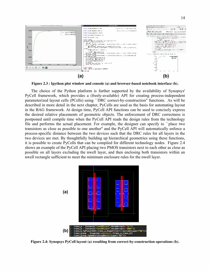
Figure 2.3 : Ipython plot window and console (a) and browser-based notebook interface (b). .... 14
Figure 2.4: Synopsys PyCell layout (a) resulting from correct-by-construction operations (b). .. 14
Figure 2.5 : BAG class structure UML diagram. .......................................................................... 16
Figure 2.6: TestbenchModules with a single DUT before (a) and after (b) automatic DUT detection and with multiple DUTs before (c) and after (d) user-specified DUT detection. .................................................................................................................... 19
Figure 2.7: NMOS primitive device class schematic template and three example instances with different parameters. ................................................................................................... 21
Figure 2.8: Extracted capacitor density and bottom plate ratio simulation results (b) for a unit capacitor PyCell (a) in commercial CMOS 40nm and 65nm processes. ................... 22
Figure 2.9: Sizing three inverter chain using LogicalEffort’s size_for_effort() function. ............. 23
Figure 2.10: Three specific instances of a variable structure architecture for a resistor string DAC with bits = 2, radix = 4 (a), bits = 3, radix = 4 (b), and bits = 3, radix = 2 (c). .......... 24
Figure 2.11: First design flow step of a power-gated NOR driver (a) illustrating parameterized schematic entry (b). .................................................................................................... 25
Figure 2.12: Automatically created class stub of a power-gated NOR. ........................................ 25
Figure 2.13: Interactive schematic exploration of a power-gated NOR. ....................................... 26
Figure 2.14 : Fully automated PyCell generation of a power gated NOR. .................................... 27
Figure 2.15: Interactive layout exploration using PyCell Explorer. .............................................. 27
Figure 2.16: Interactive schematic exploration with post-layout extraction. ................................ 28
v
Figure 3.1: Instances of an amplifier PyCell compiled using a 65nm (a) and 40nm (b) technology file and of a network of power switches and drivers compiled using a 65nm (c) and a 40nm (d) technology file. ........................................................................................... 30
Figure 3.2: BAG layout generator flow. ........................................................................................ 31
Figure 3.3: Standard Cell layout style. .......................................................................................... 32
Figure 3.4: A 5-transistor amplifier PyCell (a) after sequentially lowering the vertical pitch (b), increasing the rail width (c), balancing the NMOS and PMOS ratios (d), adding dummies (e), and increasing the channel length (f). .................................................. 33
Figure 3.5: 5-transistor amplifier schematic. ................................................................................. 34
Figure 3.6: Initial placement of a 5-T amplifier in the Standard Cell style. ................................. 34
Figure 3.7: Automatic resizing of device groups in a standard cell in order to fit within the user-specified vertical pitch. ............................................................................................... 35
Figure 3.8: Two DRC errors and their associated fixes performed during the routing repair step. .................................................................................................................................... 36
Figure 3.9: 5-transistor amplifier layout after initial routing (a) and routing finalization (b). ...... 36
Figure 3.10: Standard Row style cell. ............................................................................................ 37
Figure 3.11 Standard Block style. ................................................................................................. 37
Figure 3.12: Two spacer cell instances (a) and the usage of spacer cells to prevent DRC errors during cell placement (b). ........................................................................................... 38
Figure 3.13: A Standard Block cell after initial placement with (a) and without (b) power rails and the same cell after the first routing step where a single vertical routing channel has been placed in the rightmost bundle. ................................................................... 39
Figure 3.14: During the initial routing phase a Standard Block cell has all top level pins assigned to a vertical channel (a), has horizontal channels assigned to all intra-row nets (b), and then has a vertical channel assigned for any inter-row nets (c). .......................... 39
Figure 3.15: A Standard Block cell is finalized by adding a power grid (a), trimming and reorganizing routes (b), and rerouting the power rails on each row (c). .................... 40
Figure 3.16: Array style floorplan of top level array and example layout of a unit cell. .............. 41
Figure 3.17: Using only the highlighted vias and stiches, a unit cell (a) can be configured for control by an odd bit (b), control by an even bit (c), or configured as a dummy cell (d). .............................................................................................................................. 41
Figure 3.18: Three instances of binary weighted DACs 2, 3, and 4 bits. ...................................... 42
Figure 4.1: Switched-capacitor Operation. .................................................................................... 45
Figure 4.2: A lower bound hysteretic control circuit (a) used to control a switched-capacitor converter unit cell (b) and the waveforms (c) depicting its operation. ....................... 46

vi
Figure 4.3: Implemented SC Converter regulation loop with asynchronous lower bound control and its behavior in the presence of a load current step. .............................................. 47
Figure 4.4: Switched-capacitor Regulator Generator. ................................................................... 48
Figure 4.5: SC Interleaved Phase schematic (a) and layout (b). .................................................... 49
Figure 4.6: Control core critical path. ............................................................................................ 50
Figure 4.7: Asynchronous comparator PyCell compiled with 65nm and 40nm technology files. 50
Figure 4.8: Control Block PyCell. ................................................................................................. 51
Figure 4.9: Power switches and drivers. ........................................................................................ 52
Figure 4.10: Power switch PyCell (a), M7 driver schematic (b), and M5 driver PyCell (c). ........ 53
Figure 4.11: A binary search matches the width of the top row of power switches and drivers with the bottom row (a)-(c) before the final M5 switch placed (d). The actual layout is overlaid by the cartoon in (e). ................................................................................. 54
Figure 4.12: Bias DAC unit elements configured as a basic unit cell, a bias cell, and a dummy cell. ............................................................................................................................. 55
Figure 4.13: Bias Current DAC layout instances for 2 and 4 bit configurations. ........................ 56
Figure 4.14: Load DAC array and slew rate limiter schematics. .................................................. 57
Figure 4.15: Load DAC unit elements configured as a basic unit cell (with an even or odd control bit) and a dummy cell. ................................................................................................ 57
Figure 4.16: Load DAC final layout with slew rate limiter. .......................................................... 58
Figure 4.17: 6-phase instance of an interleaved switched-capacitor converter with per-phase lower bound control blocks. ....................................................................................... 59
Figure 4.18: Final layouts of three complete SC regulator designs. .............................................. 60
Figure 4.19: Load transient step response simulation result. ........................................................ 60
Figure 4.20: Generated AMS instance combined with a synthesized digital block. ..................... 61
Figure 5.1 Manual PyCell of a comparator. .................................................................................. 64

vii
List of Tables
Table 2.1: Subjective comparison of scripting language choices for creating an AMS circuit generator framework. ................................................................................................. 13
Table 4.1: Switched-capacitor Regulator Target Specifications. .................................................. 48

viii
Acknowledgements Many people contributed to the work presented in this thesis both directly (through work on
the BAG project) and indirectly (through their influence on and connections to me) and I would like to take some space to express my gratitude to them.
First, I would like to thank my advisor, Prof. Elad Alon. A fellow student and I were walking back from dinner with Elad during a tapeout period and the topic of discussion turned towards what we would do in life if we could choose anything and earning money and aptitude for the activity were non-issues. I couldn't come up with anything specific but after having been in tapeout mode for several weeks I said it would definitely be something more fun and less exhausting than designing circuits. The other student replied that he would probably like to play basketball all day. I agreed that would be a good choice and then we both looked towards Elad. He didn't have to say anything but I think all three of us knew the answer. There is nothing Elad would like more than researching, teaching, speaking, and writing about a topic he loves. There is no better quality that a student could hope to find in an advisor and there is no better advisor a student could hope to find than Elad.
I would also like to thank all of the faculty at Berkeley that have helped me during my time here. I am particularly grateful to Prof. Ali Niknejad for serving on my quals committee, reading this thesis, and for teaching the two most challenging circuits classes I ever took. I am indebted to Prof. Bernhard Boser for the advice that led me to join Elad’s group and to Prof. Paul Wright for agreeing to read this thesis at the last minute. I would also like to thank Prof. Vivek Subramanian and Dr. Reza Moazzami for teaching classes that were so interesting that I signed up to take one of their other courses (which wasn’t initially my plan).
The Berkeley Wireless Research Center (BWRC) has been a big part of my life at Berkeley and I would like to thank all of the faculty and staff there. I especially appreciate those who helped me wrestle with CAD tools and computers: Brian Richards, Ken Tang, Kevin Zimmerman, Brad Krebs, and Ubirata Coelho.
I would also like to thank all the advisors and administrators who made my experience at Berkeley as smooth and stress-free as possible: Ruth Gjerde, Shirley Salanio, Olivia Nolan, Leslie Nishiyama, and Tom Boot.
I worked with many fellow students over the years for research and/or class projects and I would like to thank some of them (in no particular order): Eun Ji An, Bonjern Yang, Nicholas Sutardja, Kwangmo Jung, Lingkai Kong, Simone Gambini, Rikky Muller, Lingkai Kong, Yue Lu, Seobin Jung, Chintan Thakkar, Jaeduk Han, Hanh-Phuc Le, Rachel Nancollas, Alberto Puggelli.
Finally, I would like to thank Megan for sticking with me through everything. It is entirely her doing that I have now accomplished what I’m sure will be one the proudest achievements of my life: making it through a Berkeley PhD with my sanity and relationship in tact.

1
Chapter 1 – Introduction
1.1 The case for analog design automation The recent trend in embedding multiple applications into a single System-on-Chip (SoC) has
resulted in a substantial increase in the number of digital and Analog/Mixed-Signal (AMS) components integrated per die [1]. Although the core functionality in such integrated systems is often implemented with digital circuitry, some functions that are required to guarantee system functionality and performance (e.g. radio transceivers, temperature sensors, voltage regulators, high speed IO, PLLs) rely on AMS design techniques. Compared to digital circuit design flows, AMS circuit design lacks a common set of well-defined steps in the design flow or the ability to capture a design procedure in an executable way. As a result, even though digital circuits dominate in terms of their total die area – as shown in the A7 SoC in Figure 1.1 – AMS circuits are increasingly the gating factor preventing designs from being completed on time and/or within budget.
Figure 1.1: Apple A7 SoC with some of the AMS blocks highlighted [2].

2
As shown in the example AMS design flow of Figure 1.2, AMS designers are directly involved in many steps of the design process, and are also critical in connecting the various steps into a cohesive design flow. While some individual steps – like SPICE simulation and parasitic extraction – do not require a human-in-the-loop1, others (e.g. custom layout) require extensive manual labor. Even the automated steps still require designers to interpret the results, modify design parameters, and pass information to other steps of the design. In contrast, digital design flows centralize all manual efforts into a set of design scripts. The steps of the digital design process, all of which are highly automated, are then connected and controlled from the script rather than directly by the designer. Once a design script has been fully debugged, it is usually possible to modify the inputs (e.g. to modify register transfer language (RTL) descriptions or update the standard cell libraries) and successfully rerun the design procedure without requiring additional work from the designer.
Figure 1.2: Digital vs. AMS design flow.
Today’s AMS design flows unfortunately do not have the same property. In fact, the amount of human intervention required for AMS designs is actually increasing due to the increasing interaction between the layout design steps and circuit performance that occurs as designs are started in or migrated to more advanced technology nodes. Creating and verifying “high-quality” (i.e., meeting performance/power as well as reliability/yield constraints) layouts is perhaps the largest single task in a typical AMS circuit design. Unlike digital flows, the layout designer usually still hand-places devices and draws polygons for routing. If manual layout were just a matter of a single continuous process, one time for every tapeout, without requiring any modifications or restarts along the way, it might not be such a big time sink. Unfortunately that situation almost never occurs. Unless the designer has very accurate initial layout parasitics, it is usually the case that after the first-pass layout is completed and the circuit is simulated to include the extracted parasitics, the whole design sizing must be performed again. This of course, leads
1 SPICE circuit simulation takes a netlist and a testbench script as inputs and produces as output
calculated voltages and currents for the nodes and branches of the circuit. While human involvement may be used to produce the inputs and examine the outputs, the process of solving the differential equations is fully automated. Designers tend to take this kind of automation for granted because the amount of effort for the equivalent manual procedure is so high that it is not considered a viable option. Layout parasitic extraction is similarly automated and accepted as the standard.
6LPXODWLRQ
&XVWRP�/D\RXW
([WUDFWLRQ
$06'HVLJQHU
6FKHPDWLF�6L]LQJ
6SHFLILFDWLRQV 7HFKQRORJ\�,QIR
'LJLWDO�'HVLJQHU
3ODFH�DQG�5RXWH
7LPLQJ�$QDO\VLV
*DWH�OHYHO�6\QWKHVLV
$06�&LUFXLW�,QVWDQFH
'LJLWDO�&LUFXLW�,QVWDQFH
'HVLJQ�6FULSW
57/ 7HFKQRORJ\�,QIR
+XPDQ�LQ�WKH�ORRS $XWRPDWHG
'LJLWDO�'HVLJQ�)ORZ $06�'HVLJQ�)ORZ

3
to changes in the layout, and if those changes are significant enough, it can require almost as much time as the first pass layout. In some cases it might even be more if the designer realizes that they neglected certain constraints during the first pass. All of this effort is only assuming a normal layout procedure and not accounting for any of the numerous layout-affecting scenarios that could result from a change in the specifications or a change to the process.
Given the labor-intensive nature of manual AMS circuit design, it would thus be highly desirable to automate the design of AMS circuits, in a manner analogous to automated digital design techniques, and foster their reuse across multiple SoCs and technology generations. This would shorten the time-to-market of new products, and would free analog designers from performing repetitive tasks (e.g. circuit redesign due to a change in the specifications or technology migration).
In order to understand the advantages that design automation can bring to AMS circuit design, it is useful to examine a representative example design that uses the traditional, manual design flow. The digital phase locked loop (DPLL) shown in Figure 1.3 is one implementation of a clock generator – which is a common AMS circuit block – that was created using a manual AMS design flow. The goal of this design was to generate a low-jitter clock in the presence of significant supply noise with minimal power consumption [3]. The most unique parts of the design were the overall architecture combining three different control paths, and the circuit techniques used to control the phase of the DCO. Most of the sub-blocks involved – such as the current DAC, capacitor DAC, low-pass filter, and phase frequency detector – used standard architectures and well-understood design procedures. Despite this, a large portion of the total work that went into the design was spent on these blocks, which although they were necessary for the correct function of the circuit, were not critical to the main advances we intended to demonstrate with the PLL architecture. From an academic perspective, automating these types of circuits could allow research to be more focused and allow less time to be spent implementing excessive amounts of ancillary circuits just to demonstrate one new idea. Automating designs like these is also attractive from an industrial perspective in order to simplify and speed up the design process as well as to improve the productivity of AMS circuit designers.
Figure 1.3: Digital PLL Block Diagram.
Ȉǻ
Ȉ
Ȉ
��'3//�ZLWK�/LQHDU�3KDVH�&RQWURO

4
Ancillary circuits are not the only type of circuits that could benefit from automation. New architectures and design techniques could spread faster and have wider impact if designers had more resources other than research papers and design review slide decks. In Figure 1.3, the linear regulator used to filter out supply noise in the digital PLL made use of design techniques from recent work on replica compensated regulators [4]. In contrast to the previously mentioned circuits, the regulator had a more direct impact on the jitter performance and supply rejection of the PLL and the chosen regulator architecture was less widely known (and more importantly, not known to the author at the time, who was the PLL designer). A research paper can be helpful when learning how to design a new circuit, but if that is the only resource available, it leaves a lot of room for misunderstanding on the part of the reader and miscommunication on the part of the writer. Having an automated design procedure for the regulator that could be examined and rerun with different parameters, even if the procedure required modifications in order to reuse it in the context of the PLL, would have been very useful in understanding the circuit, speeding up the design process, and achieving the best performance.
So far, the digital PLL example has been used to motivate the general notion of AMS circuit design automation without suggesting any specific features that should be included in an automated design flow. One feature that would have been particularly useful in the final days before the tape-out deadline of the digital PLL is a degree of programmability in the aspect ratio of the layout. Figure 1.4 shows two top-level layouts for the digital PLL that were separated in their time-of-completion by two days. The layout on the left, which measures 1x1 mm and is pin-limited, had just been completed when the foundry sent notification that the shuttle run only had room for chips with one dimension smaller than 450 um. The layout on the right was completed two days later (just in time to meet the deadline) after considerable manual layout modifications. If the foundry had specified 400 instead of 450 um, the manual layout modification effort would have been too large to meet the deadline because it would have required modification of the PLL core itself and not just the bond pads, power grid and top level routing. An automated layout procedure that could target a particular aspect ratio or constrain a single dimension of the layout would have worked in both scenarios and would have had the added benefit of giving the designer (who once again, was the author of this thesis) a lot more sleep and a lot less stress over the final two days of the tapeout period.

5
Figure 1.4: Digital PLL chip layout before and after a last minute change to the allowable dimensions.
1.2 Previous Work The idea of automating analog circuit design is by no means novel, and significant effort
using a variety of methodologies has been made to automate various steps of the AMS circuit design flow. In [5], Gielen and Rutenbar give an excellent overview of many of these efforts, which they divide into two broad categories: “knowledge-based techniques” and “optimization-based techniques”. In knowledge-based automation techniques [6], [7], design steps tailored to specific circuit architectures (e.g. Flash ADC, Switched-Capacitor filters, etc.) are encoded into a design procedure, i.e. scripts that replicate the activity of the designer. These scripts are usually fast to run, as well as serving as functional documentation of the design, and the designer maintains full control of the flow, thus easing modifications and debugging. On the other hand, the activity of setting up the scripts can be long and error prone, and new scripts are needed for each new design, so a library of design plans is required to make these approaches widely adoptable. Optimization-Based Techniques [8], [9], in contrast to knowledge-based techniques, keep the functional description of the design under analysis separated from a library of available architectural implementations. The user enters the desired system functionality in terms of behavioral models and performance constraints. Synthesis is then cast into one or more optimization problems, where the user-defined cost function and constraints drive the tool to select and size the library architecture that optimally meets the specifications. These constraint-driven approaches have been shown to produce high- performing designs, and can, in principle, seamlessly operate on a large class of AMS circuits using the same design steps. On the other hand, they can have long runtimes due to the large design space to be explored for practical analog circuits (> 100 devices), and can still require substantial design experience to properly constrain the optimizer. Further, the returned circuit implementation might be difficult to debug or modify, since the tool acts as a black-box to the user, preventing them from building intuition
0DQXDO�/D\RXW�(GLWLQJ

6
on how the design has been generated.
Despite these efforts, the AMS circuit designer community has been reticent to widely adopt automation software, remaining anchored to the highly manual nature of the custom flow. We believe that historically this reluctance has stemmed from the lingering difference in perspective between the two communities. The CAD community has mainly focused on developing modeling frameworks to capture system functionality and optimization algorithms for architecture selection and sizing, but it has left to the designers the burden of creating a library of architectures compatible with the proposed frameworks. The designer community, instead, has lamented the excessive initial effort required to set up a new automated design flow, and has shown skepticism towards automation, motivated both by the belief that a better design can be obtained through a manual effort and by the fear of losing their central role (and perhaps their job) in the design process.
This situation is now rapidly changing. The need to integrate an increasing number of AMS circuits per chip has pushed the designer community to an inflection point with regards to design automation, since: 1) the ability to quickly redesign a block now outweighs the initial effort to set up an automated synthesis flow; 2) there is a concrete request to create more designs with the same number of people, instead of the same number of designs with fewer people, and; 3) the efforts of almost three decades of research have improved the tools that can help automate individual steps in the analog CAD design flow.2 In the following chapters, we describe our effort towards enabling a widely-adopted shift in the methodology used to design AMS circuits through the creation of a design framework capable of codifying all the steps of the design flow, the development of helper classes to ease (from the designer’s perspective) the process of codifying the schematic sizing and especially the layout procedure, and the creation – using the aforementioned framework and helper classes – of circuit generators for a non-trivial circuit capable of creating multiple instantiations targeting different input specifications.
1.3 Organization Chapter 2 introduces the Berkeley Analog Generator (BAG) framework, a design framework
for AMS circuits capable of integrating all steps of the design flow, from architectural-specification definition to correct layout implementation, into procedural analog generators. A definition of an AMS circuit generator is provided followed by an explanation of the goals of the BAG project, a description of a generator design procedure, and details of the framework’s implementation. Chapter 3 focuses on the BAG framework’s approach towards automating layout by enabling designers to create layout generators for specific circuit architectures. In order to assist the designer in creating layout generators, the BAG framework provides template-based extensible layout generators for two styles of parameterized layout, suited respectively to heterogeneous and homogeneous AMS circuits. Chapter 4 presents a case study for a switched-capacitor converter generator that is used to create three converter instances targeting different output power levels and efficiencies as well as different physical aspect ratios. Finally, we conclude and discuss plans for the future of the BAG framework in Chapter 5.
2 In fact, CAD research in the field is still active, both in the academic and industrial worlds [10]–[13]
7
Chapter 2 – Berkeley Analog Generator Framework
In this chapter, we present BAG, the Berkeley Analog Generator, an integrated framework for the development of generators of AMS circuits – i.e., parametric design procedures to synthesize a schematic and layout of a circuit according to a set of input specifications. We developed BAG with the goals of closing the gap between the designer and CAD communities, and providing designers with a framework that allows them to take advantage of the CAD tools available to help automate their designs and foster reuse. Designers can use BAG to develop circuit architectures closely following all steps of their familiar custom flows. At the same time, BAG also assists them in defining an abstraction of the architecture free of most implementation details (e.g. device sizing and technological parameters) in order to create a library of components suitable to be embedded within the desired optimization framework.
Using the previously introduced classification, BAG belongs to the knowledge-based category, in that the design flow is codified as a set of procedural scripts. We believe that this approach is more likely to be adopted by the designer community, because it maintains the central role of designers. Moreover, we argue that most optimization- based techniques proposed in the literature still require substantial design experience to produce high-quality results. At the same time, though, they enforce algorithmic steps in the design flow that can prevent the designer from fully driving the project towards the desired direction. We chose a dual approach. The basic version of the proposed flow is knowledge-based, so that the designer can maintain control. Specific sub-tasks can then be automated at the will of the designer to improve runtime and/or design performance. Instead of designing a specific circuit instance as in the standard custom flow, the designer uses BAG to develop a circuit generator, agnostic towards technology information and parameterized by the desired input specifications. The time overhead in setting up the flow is thus amortized by reusing the generator to synthesize circuit instances with varying input specifications and across technology nodes. The availability of circuit generators also eases hierarchical top-down design, where complex blocks recursively instantiate sub-components fulfilling specifications propagated from the higher level.
2.1 What is an AMS circuit generator? An AMS circuit generator is a set of design functions that can create a fully sized schematic
and a layout of a circuit according to a set of input specifications. Any such generator should, at a minimum, be capable of reading a set of input specifications, automatically sizing all schematic components, generating a corresponding physical layout that meets all design rules and Layout Versus Schematic (LVS) checks, and outputting the resulting circuit performance, which need to meet all specifications while optimizing some application-specific figure of merit. Borrowing terminology and graphical representation from the Unified Modeling Language (UML) [14], we thus define the interface Analog Generator shown in Figure 2.1. Each circuit generator can be implemented as a class that has to implement all the methods specified in the Analog Generator interface. Although individual generators require specific procedures to optimize the performance of the design under analysis, much of the effort in creating a generator is not unique

8
to any single circuit. An AMS circuit generator framework can thus provide a set of abstract base classes to help a designer create new generators by providing interfaces to tools that perform common functions in the design process. Figure 2.1 shows an example of some of these functions as part of a sample abstract base class from which all analog generator classes could inherit.
Figure 2.1 : AMS circuit generator interface and an example abstract class implementation of the interface.
In our approach to analog circuit design automation, a designer’s deliverable is not a single instance of a sized schematic and clean layout for a particular circuit, but rather a generator for a desired class of circuits. These generators can replicate, in an automated fashion, the design procedure that would have been used for a traditional, manual design.
2.2 Goals for the BAG Framework The primary goal of the BAG project is to provide a framework that encourages and enables
circuit designers to become circuit generator designers. To that end, given the poor adoption rate of existing automation tools, there are several important aspects that we try to address in order to create a framework that designers can and will actually use. These aspects, which will be described further in this section, are: completeness, ease of adoption, and ease of reuse.
Completeness 2.2.1An automation framework that only focuses on a portion of the design procedure can be very
useful, but is much less likely to be adopted in the long run. Many of the key benefits of automation, including the ability to rapidly adapt and reuse pre-existing designs and perform quick design iterations, are precluded if the framework requires substantial manual effort for even a single design step. As an example, the performance of AMS circuit designs, especially those made in today’s advanced technology nodes, are greatly impacted by the effect of layout parasitics. Therefore, including some form of layout automation in the framework is vital in order to enable meaningful design iterations that do not require massive amounts of manual tweaking, or worse – complete redesign – when translated from schematic to layout.
��,QWHUIDFH!!$QDORJ�*HQHUDWRU
5HDG6SHFLILFDWLRQV��'HVLJQ6FKHPDWLF��'HVLJQ/D\RXW��9HULI\$UFKLWHFWXUH��:ULWH3HUIRUPDQFHV��
��$EVWUDFW�&ODVV!!0RGXOH
VSHFV��6SHF> @SHUIV��3HUI> @&RGH6WXE*HQHUDWLRQ��5XQ2SWLPL]HU��/DXQFK6LPXODWLRQV��5XQ'5&��5XQ/96��*HQHUDWH6L]HG6FKHPDWLF��

9
Remaining comprehensive in the face of advancements in design tools depends on the framework being extensible. One way to ensure a framework remains complete is to hire a group of developers to maintain and enhance the framework. Another way, which is much more feasible for an academic project, is to allow the same community that uses the framework to modify and improve the source code of the framework itself. In order for this method to work, the framework must be adopted by a large enough number of people so that the small fraction who actually contribute useful code are sufficient to cover a large variety of design techniques and tools necessary for a truly comprehensive framework. One way to encourage this is to release a framework’s source code3 under an open source license using a collaborative source code revision control tool such as GIT [16]. This doesn’t guarantee that people will use the framework or contribute improvements or bug fixes, but at least it enables the widest possible audience and hopefully improves the odds of finding enough contributors to maintain the framework.
Ease of Adoption 2.2.2Conventional wisdom says you never get a second chance to make a good first impression.
The first impression a new user forms of a design system highly depends on the effort, and especially the amount of time, required to start using the system effectively. The more difficult and the longer this time period, the more the designer will resist trying the tool and the less likely they will be to adopt it in the long term. In order to minimize this time, an AMS automation framework must build on the base-level of knowledge and common skill-sets possessed by most AMS designers, and must do so in a way that seems somehow familiar to the designer.
Allowing designers to codify their existing design procedures, rather than forcing them to conform to a specific design style will let designers more readily adapt to a generator-centric design methodology. If they have to learn a new or unfamiliar design style, whether it be optimization-based or knowledge-based, in addition to a new framework of tools for executing the design process, they will then require more time to adapt which might provide an excuse to dismiss the tool completely.
Another way the framework can reduce the initial learning curve is to provide an intermediate step between a manual, hand-tweaked circuit design and a fully scripted circuit generator. An interactive, console-based script interface can serve as this intermediate step by allowing the designer to explore the design manually using traditional techniques but still using the same functions that will eventually be used for the fully scripted generator. In this way, the task of writing the generator code can be made somewhat less difficult as the designer can adapt code fragments from the command history of the interactive session and there can be less duplication of design effort.
3 A pointer to the BAG framework source code can be found [15]

10
Ease of Reuse 2.2.3While it is important to reduce the difficulty of the designer’s first experience with writing a
generator, it is equally important that their subsequent experiences offer substantial time savings compared to standard design practices, otherwise the designer will have no incentive to continue using it. To that end, an AMS automation framework must encourage and enable simple reuse mechanisms. A common scheme used to simplify the reuse of a complex codebase is object-oriented programming (OOP) [17].
There are many resources available that expound at length on the topic of object-oriented programming [18], [19], so this section will only present the handful of OOP concepts that are particularly useful to the task of creating a reusable AMS automation framework. One of these concepts is encapsulation, which dictates that data and the procedures that operate on that data are grouped together in self-contained bundles called objects. Objects of the same type, i.e. containing the same categories of data (though not necessarily the same data) and the same operations, are said to be instances of a particular class of objects. An object is a natural representation for a circuit model since a circuit is something that has certain attributes, e.g. connectivity and sizing, but also performs a particular operation amongst inputs and outputs. In order to create a design framework for circuit generators, we merely have to extend the concept of a circuit as an object to include all the operations and data necessary for the design procedures that produce an instance of a circuit instead of just the end result. OOP also enables direct reuse of code by enabling classes to inherit functionality and data in a hierarchical fashion from higher-level classes. This concept can easily be applied to circuits that belong to the same class to provide certain functions that are shared by all circuits of that class such as simulation testbenches, e.g. a phase noise simulation testbench that works for both LC and ring oscillators.
A final factor impacting the reusability of generators designed using a particular framework is the structure of the framework itself. If interfaces are defined inappropriately, it can be difficult to encapsulate the shared functionality of the generators. Similarly, if circuit generators are created at too high a level within the circuit hierarchy, there won't be very much reuse. As an extreme example, if a PLL was created as a single monolithic generator made up of primitives, i.e. no sub modules are themselves generators, then nobody would be able to reuse the charge pump or VCO from the PLL for other circuits without substantial modification to the generator code.
2.3 Framework Implementation A set of abstract goals is not sufficient information to begin working on a complex codebase.
Before an actual generator framework can be created, several questions must be answered: What will the design flow for creating a generator for a new circuit architecture look like? What programming languages and tools will be needed to build a framework that enables this design flow? How will the framework be organized? This section will answer these questions with regard to the development of the BAG framework and also describe a set of useful helper classes that, while not required to implement the interface defined in Figure 2.1, help the BAG framework achieve some of the goals of the previous section.

11
Generator Design Flow Description 2.3.1Although the end product is a collection of code, as shown in Figure 2.2, the BAG design
flow begins in much the same way as an instance-based, manual design flow – i.e. by capturing a specific circuit architecture in schematic form. However, instead of entering a sized schematic, the designer creates a parametric schematic where only the connectivity among circuit devices is fully specified, while neither device sizes nor process information are provided. The purpose of the parametric schematic is to annotate as much of the designer's intent as possible [20]. In order to do so, we created technology-agnostic primitive devices (e.g. NMOS and PMOS transistors, resistors, capacitors, etc.), whose sizes can be left blank (to be filled in later) or assigned meaningful parameter names to express, e.g., matching and ratio constraints. Primitives can also be assigned specific intent, e.g. a transistor can be annotated as fast or low power.
Figure 2.2: Design flow used to produce a generator using BAG (a) and the generator execution process to produce a circuit instance (b).
Next, the designer creates a parametric testbench schematic in the same manner used for the design schematic, and enters the associated simulation setup -- including simulation type, simulation parameters, and probe points -- through Cadence ADE [13]. Testbench schematics in BAG are atomic, i.e. only one simulation per testbench, which improves their reusability. The parameterized design and testbench schematics are imported recursively in BAG and used to create stub class definitions, which inherit from the DesignModule and TestbenchModule classes respectively, for every unique cell in the hierarchy.
Since it is difficult to design a technology independent generator without being able to debug or test it using a real technology, the recommended BAG design flow entails the selection of a representative process technology for use in the next steps of the design flow. By forcing the designer to access all technology-specific information through a well-defined interface, the job of translating the technology-dependent design exploration into a technology-independent generator is made more tractable, reducing the burden on the designer. Ultimately, however, the process independence of a generator does depend on the designer.
%$*�*HQHUDWRU�([HFXWLRQ%$*�*HQHUDWRU�'HVLJQ�)ORZ
,QWHUDFWLYH�6FKHPDWLF�([SORUDWLRQ
6FKHPDWLF�6L]LQJ�&RGLILFDWLRQ
/D\RXW�'UDZLQJ�&RGLILFDWLRQ
/D\RXW�([SORUDWLRQ
3DUDPHWULF�6FKHPDWLF�&UHDWLRQ
3DUDPHWULF�7HVWEHQFK�&UHDWLRQ
&RGH�6WXE�*HQHUDWLRQ
*HQHUDWRU
6SHFLILFDWLRQV 7HFKQRORJ\�)LOH
([WHUQDO�7RROV
&LUFXLW�,QVWDQFH
�D� �E�

12
Once the initial classes for the design under development and its associated testbenches are created, and an initial process technology has been selected, the designer can then – without writing any code – create an instance of the design. In the traditional flow, the designer debugs and explores the design by choosing some initial sizing, simulating, viewing the results, and iteratively adjusting the sizing until specifications are met. This flow can be replicated in BAG, with the important difference that the exploration is done in an interactive, code-based environment. Performing the initial exploration using the same code constructs that will be used in the final generator is key to lowering the designer effort in writing the generator code. For example, snippets of code used in the exploration process can be used to build DesignSchematic() and VerifyArchitecture() methods that are required to implement an Analog Generator interface, as defined in Figure 2.2.
The next step is creating a parameterized layout. Similar to the exploration step for schematic sizing, the designer can view the layout in an interactive environment where they can test changes before incorporating them into a DesignLayout() function. Once an initial layout has been created, the designer can return to the interactive environment and run physical verification checks – Design Rule Checking (DRC) and Layout Versus Schematic (LVS) –to then be added to a VerifyArchitecture() function. The designer can modify the layout and iterate until the design is DRC and LVS clean. The layout parasitics can then be extracted and post-layout simulations run. Using the results of these simulations, the designer can revisit the DesignSchematic() function and modify it as necessary to account for layout effects. Given the importance of these effects on designs in modern technologies, it can be useful to perform the layout generator creation step earlier – before spending much time on the DesignSchematic() function – since any design procedure developed without reasonable estimations of the layout effects would need to be modified later in any case.
After the initial pass through the design flow, the designer can iteratively refine the generator class to improve the design’s performance, e.g. by calling numerical or equation based optimizers, and/or make the generator faster, more robust, and more reusable. In a complete generator, all knowledge of the design should be codified in the generator class definition. Once the generator is complete, the designer can pass input specifications and technology information to it in order to produce unique design instances of an architecture, as depicted on the right side of Figure 2.2.
Language and Tools 2.3.2Several platforms were considered for implementing the BAG framework, including Matlab,
Perl, Python, SKILL and Tcl. Table 2.1 shows a mostly subjective comparison of these languages. For a more objective analysis, see [21]. All of the languages have some strong points. SKILL is a proprietary language tied strongly to Cadence’s Virtuoso, the most popular existing analog CAD tool suite, but it lacks the breadth of functionality available with most of the other languages. Perl has a lot of useful libraries available and is quite fast, but is notoriously difficult to read. Tcl is a popular choice in electronic design automation (EDA) tools and is generally easier to understand than Perl, but it lacks speed and has fewer useful libraries. Matlab is easy to use and has an excellent interactive shell, but it is also somewhat slow, and its object-oriented features are less mature than many of the other languages.

13
Ultimately, Python was chosen as the implementation language for several reasons. It has strong support for object-oriented features such as abstract base classes and multiple inheritance which can help achieve the desired goals of easy extensibility and reuse. Additionally, Python’s indentation-based structure and highly readable syntax are well suited for inexperienced or novice programmers4. It is also fast, both in terms of execution time and the amount of time required to create working code.
TCL Python Perl Matlab SKILL
Code Readability Good Excellent Bad Good Fair OOP Tacked On Built in Tacked On Tacked On Tacked On External Libraries Fair Excellent Good Good Bad Interactive Shell Yes Yes No Yes Yes Speed Fair Good Good Fair Fair
Table 2.1: Subjective comparison of scripting language choices for creating an AMS circuit generator framework.
More expressive generators can be written by leveraging the plethora of off-the-shelf packages provided in Python, ranging from numerical and scientific computing (NumPy [22] and SciPy [23]), to graphical plotting (Matplotlib [24]), and numerical optimization (e.g., CVXPY [25]). Python also has a powerful interactive command line that can enable generator designers to rapidly iterate during the generator codification process. The default python console provides most of this functionality, but there are other add-ons for python, namely Ipython [26], that offer even more integration of the aforementioned tools. Ipython provides a pylab mode that integrates NumPy, SciPy, and Matplotlib functionality into the console along with improved code completion and debugging tools. Figure 2.3(a) shows a plot result from a simulation run from the pylab console. Recent versions of Ipython introduce a notebook mode, similar to Matlab’s cell mode [27], where scripts can also be written in an active document format that can be edited and run from a web browser. Results, in the form of standard output text and inline graphics can be saved along with the script itself. This format, show in Figure 2.3(b), can be useful for debugging scripts because the user can rerun certain cells without rerunning the whole script. It is also useful for recording the results of a scripting session along with detailed documentation that can be inserted inline with the code using a simple, wiki-like markup language.
4 Increasingly, AMS circuit-designers coming out of school have a substantial amount of practical
programming experience, so this point is less critical than it may have been in the past.
14
Figure 2.3 : Ipython plot window and console (a) and browser-based notebook interface (b).
The choice of the Python platform is further supported by the availability of Synopsys' PyCell framework, which provides a (freely-available) API for creating process-independent parameterized layout cells (PCells) using ``DRC correct-by-construction" functions. As will be described in more detail in the next chapter, PyCells are used as the basis for automating layout in the BAG framework. At design time, PyCell API functions can be used to concisely express the desired relative placements of geometric objects. The enforcement of DRC correctness is postponed until compile time when the PyCell API reads the design rules from the technology file and performs the actual placement. For example, the designer can specify to ``place two transistors as close as possible to one another'' and the PyCell API will automatically enforce a process-specific distance between the two devices such that the DRC rules for all layers in the two devices are met. By thoughtfully building up hierarchical geometries using these functions, it is possible to create PyCells that can be compiled for different technology nodes. Figure 2.4 shows an example of the PyCell API placing two PMOS transistors next to each other as close as possible on all layers excluding the nwell layer, and then enclosing both transistors within an nwell rectangle sufficient to meet the minimum enclosure rules for the nwell layer.
Figure 2.4: Synopsys PyCell layout (a) resulting from correct-by-construction operations (b).
�D� �E�
�D�
�E�

15
The PyCell API is also part of the interoperable process design kit (iPDK) specification [28]. The iPDK is an attempt by a large group of EDA vendors and foundries (most notably TSMC), to create an interoperable custom design framework. It is built around the already widely-adopted OpenAccess [29] design database and uses PyCells to provide parameterized layout cells. At the time of the writing of this dissertation, it seems that the iPDK, and through it the PyCell API, is seeing increasing adoption. Correct-by-construction operations are extremely useful, but if no foundry offers a PDK that supports PyCells, then it wouldn’t make sense to include them in the framework.
Although support for open standards is not a primary goal of the BAG framework, we tried to choose open tools and APIs whenever possible to ensure the most interoperability and reduce dependence on proprietary standards that can change at the whim of a single EDA company. The code for the Synopsys tools used for creating PyCells, while not open source, is held in escrow with the condition that, should Synopsys ever stop offering it free of charge or providing support, the source will be released to Si2, the industry organization responsible for maintaining the OpenAccess API. We also tried to give the designer freedom of choice in terms of design tools by identifying the core functionality required for the design flow and defining a standard interface between that core functionality and the specific tools used to provide that functionality. In practice, although we have tried to define a general interface that could enable any EDA tool to be incorporated into the BAG framework, in most cases we have initially only enabled a single tool for each piece of the design flow.
Code Organization 2.3.3The codebase for the BAG framework can be split roughly into two groups of classes as
depicted in Figure 2.5. The generator description group contains classes used to express the design itself, including the physical connectivity, device sizes, and the design procedure. In some sense, these classes provide all the functionality needed for a circuit designer to write a generator. What they lack is the ability to generate a specific instance of a circuit. The generator session group contains classes that provide interfaces to all the external tools and process information that are necessary to execute a generator and produce a circuit instance in a given technology. The central classes5 for the generator description and generator session groups are Module and BagProject respectively. This section will describe the division of functionality and design data amongst these, and other, classes.
5 These classes are important to making a functional framework and so need to be understood, but
they do not present particularly interesting challenges. The more compelling contributions of this work are the helper classes covered in 2.3.4 and the layout styles in Chapter 3.

16
Figure 2.5 : BAG class structure UML diagram.
2.3.3.1 Generator Session Classes We define the generator session as the process of executing a generator to produce an
instance of a particular circuit. The purpose of the BagProject class is to store information related to the generator session as well as interfaces to external tools required during the generator session in a central location that can be easily referenced from anywhere in the generator code. It is important that these interfaces not incur excessive execution-time overhead, i.e. on top of the inherent overhead of the tool being interfaced. This section will describe further the primary child classes of BagProject: DBAccess, DBInterface, CDFInterface, and Technology.
2.3.3.1.1 DBAccess Many of the external tools interfaced by the BAG framework belong to the Cadence Virtuoso
[13] design suite. The purpose of the DBAccess class is to provide a single interface point for all the classes in the BAG framework that need to access Cadence tools such as those for setting CDF parameters (CDFInterface) and those for running the Cadence simulation environment (OceanSimulator and SpectreSimulator). There were several alternatives for implementing this interface. One option to transfer data between Cadence and the BAG framework was to wrap the Cadence Integrator’s Toolkit C API with Python using SWIG [30] or a similar automated software interface generator. We chose not to do this because the integrator toolkit only provides functions for accessing the design database, and not for running the full set of tools in the design suite such as the Spectre circuit simulator. Another option was to launch specific Cadence executables using python’s os.system() function and redirect the output to a file for eventual parsing. We also rejected this method for two reasons. First, it blocks the execution of subsequent python code until the executable process exits. Second, it leads to wasted time loading and reloading the executable. The full Virtuoso executable can take several seconds to load so if the BAG framework calls low-level – i.e. usually quick execution time – functions from Cadence, the overhead of launching and killing the executable process becomes unacceptably large. In order to avoid this penalty, the BAG framework launches a single
0RGXOH7HVWEHQFK0RGXOH
'HVLJQ0RGXOH 3ULPLWLYH0RGXOH
&DS0RGXOH
5HV0RGXOH
0RV0RGXOH'HVLJQ3DUDPHWHU
3\1HWOLVW
2$,QWHUIDFH
6LPXODWRU,QWHUIDFH
2FHDQ6LPXODWRU
6SHFWUH6LPXODWRU0HDVXUH &RUQHUV
7HFKQRORJ\
%DJ3URMHFW6NLOO&'),QWHUIDFH'%$FFHVV
$JJUHJDWLRQ��³KDV�D´�
%LGLUHFWLRQDO�$VVRFLDWLRQ
,QKHULWV
*HQHUDWRU6HVVLRQ&ODVVHV
*HQHUDWRU'HVFULSWLRQ&ODVVHV

17
Cadence process and leaves it open during the whole design session, passing information back and forth between the framework and Cadence as necessary.
The communication between the BAG framework’s DBAccess class and the Cadence executable is facilitated by the Pexpect module [31]. Pexpect is used to spawn an interactive console-based process and control it through code using a query/response interface rather than through direct user input. Pexpect allows the BAG framework to have a virtual Virtuoso console running in the background in order to run SKILL commands and scripts. It also allows non-blocking execution so the process can continue running in the background for the whole design session. Other classes that require access to Cadence tools contain a link to the generator session’s BagProject object and consequently a link to the DBAccess object and Cadence executable.
2.3.3.1.2 DBInterface & OAInterface Custom circuit designs are typically stored in a database that groups together the schematic,
symbol, layout, and other data regarding a particular cell into a single library entry. Since the BAG framework is intended to be as tool-agnostic as possible, an abstract base class called DatabaseInterface defines a generic interface to a design database. The two main design databases are the OpenAccess and the CDBA databases. The BAG framework currently only has a subclass for the OpenAccess database called OAInterface. OpenAccess was chosen over CDBA as the initial database implementation because it is non-proprietary and used by all the major custom circuit design suites from the top EDA vendors.
The OAInterface class has functions used to instantiate layout instances used for DRC, LVS, and extraction. It also has functions to help create sized schematics by copying and modifying template schematics. OAInterface depends on a python module [32] that has python wrappers for the OpenAccess C++ API6. This functionality could also have been provided by the Cadence Integrator’s toolkit C API, but that would have required extra effort to wrap the C API with Python. Another option was to use Cadence’s SKILL API for modifying the OpenAccess database, but we chose using the OpenAccess API directly to remain as tool-agnostic as possible.
2.3.3.1.3 CDFInterface & SkillCDFInterface The OpenAccess database, though quite extensive, neglects to provide a standard mechanism
for storing and modifying the user-settable parameters associated with schematic cells or for the callback functions associated with these parameters. These parameters, or common description format (CDF) parameters (based on Cadence’s name for them), are used to store parameters like transistor width and length, model information to be used for simulation, and other electrical and geometric attributes of the device or cell they are associated with. The CDFInterface class
6 The Python OpenAccess wrappers used in the BAG framework have recently been fully rewritten
and integrated into a comprehensive tool called OaScript [33] that provides wrappers for the OpenAccess API in four common scripting languages: Python, TCL, Ruby, and Perl. Future versions of the BAG framework should switch to the new wrappers as they are better tested and much more likely to be supported over the long term. This should have no impact on the external interface of the OAInterface. class though so other classes that depend on OAInterface should not be affected.
18
provides a set of functions to read and write CDF parameters in BAG. For our implementation, because of our choice of the Cadence Virtuoso suite as the initial schematic entry tool, we implemented a subclass of CDFInterface to enable access to Cadence’s CDF parameters through the SKILL language API. This class, SkillCDFInterface, depends on the DBAccess class for access to the Cadence process that is required to execute any SKILL code. In the future, a subclass of CDFInterface could be written to support the iPDK’s TCL-based iCDF parameters or other proprietary CDF alternatives.
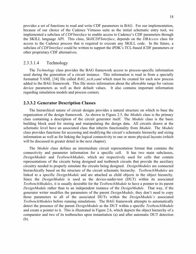
2.3.3.1.4 Technology The Technology class provides the BAG framework access to process-specific information
used during the generation of a circuit instance. This information is read in from a specially formatted YAML [34] file called BAG_tech.yaml which must be created for each new process added to the BAG framework. This file stores information about the allowable range for various device parameters as well as their default values. It also contains important information regarding simulation models and process corners.
2.3.3.2 Generator Description Classes The hierarchical nature of circuit designs provides a natural structure on which to base the
organization of the design framework. As shown in Figure 2.5, the Module class is the primary class containing a description of the circuit generator itself. The Module class is the basic building block used for storing and manipulating the design data. All circuits drawn at the schematic level have an associated class that inherits functionality from Module. The Module class provides functions for accessing and modifying the circuit’s schematic hierarchy and sizing information as well as for linking the logical connectivity to one or more physical layouts (which will be discussed in greater detail in the next chapter).
The Module class defines an intermediate circuit representation format that contains the connectivity and parameter information for a specific cell. It has two main subclasses, DesignModule and TestbenchModule, which are respectively used for cells that contain representations of the circuits being designed and testbench circuits that provide the auxiliary circuitry needed to properly simulate the circuits being designed. DesignModules are connected hierarchically based on the structure of the circuit schematic hierarchy. TestbenchModules are linked to a specific DesignModule and are attached as child objects in the object hierarchy. Since the DesignModule is used as the device-under-test (DUT) within its associated TestbenchModules, it is usually desirable for the TestbenchModule to have a pointer to its parent DesignModule rather than to an independent instance of the DesignModule. That way, if the generator writer modifies the parameters of the parent DesignModule, they don’t need to copy those parameters to all of the associated DUTs within the DesignModule’s associated TestbenchModules before running simulations. The BAG framework attempts to automatically detect the presence of the parent DesignModule as the DUT within a specific TestbenchModule and create a pointer to it. This is illustrated in Figure 2.6, which depicts the object hierarchy of a comparator and two of its testbenches upon instantiation (a) and after automatic DUT detection (b).

19
Figure 2.6: TestbenchModules with a single DUT before (a) and after (b) automatic DUT detection and with multiple DUTs before (c) and after (d) user-specified DUT detection.
Figure 2.6(c) shows a TestbenchModule used for characterizing the frequency tuning range of a supply-regulated voltage-controlled oscillator (VCO). Within the BAG framework, this TestbenchModule is associated with the PLL DesignModule rather than the VCO or regulator DesignModules. In general, TestbenchModules should be associated with the lowest level DesignModule that contains all of the DUTs used within that TestbenchModule. For simple testbench schematics that contain a single DUT, the link from the testbench DUT to the parent DesignModule is made automatically. For the PLL example shown in Figure 2.6(d), the link must be made manually in the initialization function for the PLL object.
Modules contain several attributes that store the schematic/netlist information for a circuit. Instances is a python dictionary in which the keys are the instance names of all the subcircuits of the current module and the values are the corresponding Modules associated with each instance name. The Module object also contains attributes that point directly to each of the instances listed in the Instances dictionary. This provides a shorter notation when accessing subcircuits, especially when they are several levels deep – e.g.
pll.loop_filter.amplifier.M1
instead of
pll.instances['loop_filter'].instances['amplifier'].instances['M1']
In addition to the subcircuit instance information, the connectivity for the cell is also stored in the Module object’s child objects. Pins is a dictionary that stores the input/output connection points for the current module. Connections is a list of connectivity between nets and pins, both the pins at the current level of the hierarchy and the pins of the subcircuit instances. The net information from the Connection objects can also be accessed though a child object of Module called nets.
&RPSDUDWRU
2YHUGULYH�5HFRYHU\
2IIVHW�7XQLQJ�5DQJH
&RPSDUDWRU &RPSDUDWRU
&RPSDUDWRU
2YHUGULYH�5HFRYHU\
2IIVHW�7XQLQJ�5DQJH
�D�
3//
6XSSO\�5HJXODWHG�9&2��7XQLQJ�
5DQJH
5HJXODWRU 9&2
5HJXODWRU 9&2
'HVLJQ0RGXOH7HVWEHQFK0RGXOH
3//
6XSSO\�5HJXODWHG�9&2��7XQLQJ�
5DQJH
5HJXODWRU 9&2
�E�
�F� �G�
$JJUHJDWLRQ��³KDV�D´�
%LGLUHFLWRQDO�$VVRFLDWLRQ

20
2.3.3.2.1 PyNetlist The data structures for instances, pins, and connections stored in the Module are also grouped
together in a class called PyNetlist. A PyNetlist object contains the minimal amount of netlist information to translate a Module instance to or from a schematic or netlist. The PyNetlist class can be initialized from a YAML file containing the netlist information that is created directly from a schematic template made in Cadence. It can also be created from an existing Module object and then parsed to create a netlist for use in simulation or LVS operations. A PyNetlist object is essentially a generator instance or a generator skeleton that respectively contains the circuit sizing and connectivity information or a placeholder for that information. Unlike the Module objects, it does not contain any information about the design procedure.
2.3.3.2.2 Parameters Parameters are a key attribute shared by all types of Modules. They store the process-
specific sizes associated with a generated circuit instance. Each parameter has several attributes including a name, value, default value, and an optional callback function that is called every time the parameter value is updated. All the parameters for a particular Module are stored together in a dictionary-like container object that is a direct child of the Module object. Pointers to each parameter are also created as children of the Module object for ease of access. Parameters are created automatically during the template schematic and template testbench schematic import process and can also be added by the generator writer in the initialization function of a specific Module subclass.
Setting and adjusting parameter values is one of the most common tasks a generator writer must perform, so the framework provides several ways of simplifying and speeding up parameter setting. One way is by overloading the assignment operator to simplify code for setting a single parameter value. If a parameter is assigned to a Parameter object, e.g.
amp.M1.width = Parameter('width',desired_width)
then the assignment operator functions as expected. If, however, the parameter is set to a variable that stores a number, e.g.
amp.M1.width = desired_width
then the value of the existing parameter is assigned to the number in question. Without overloading the user would have to write
amp.M1.width.value = desired_width
Parameters can also be set en masse using the set_parameters() function at the Module level. By default, this function recursively sets all parameters with the specified name, and at the level of the current module and below, to a specific value. This is useful for setting default values for a module, such as channel length or multiplier, which can then be overridden on a device-by-device basis if necessary.

21
Helper Classes 2.3.4Given a particular circuit topology, a designer typically makes assumptions about which
design procedure should be used to size the circuit and how the layout should be structured. In many cases, these assumptions are shared across a specific category of circuits, so it is useful to create helper functions that aid with the specific sizing and layout procedures. The BAG framework groups them into helper classes associated with specific circuit categories in order to enable reuse and to reduce the effort required for the initial codification of a generator. This section will describe helper classes for primitive devices, custom digital logic, and circuits with connectivity that depends on the input parameters. Layout related helper classes, which we refer to as layout styles, will be described further in the next chapter.
2.3.4.1 Primitive Devices Classes and LookupTable BAG includes helper classes for primitive devices – i.e. transistors, capacitors, and resistors –
that provide the generator writer access to device characterization data for the primitive device in any technology node. This allows designers to write sizing procedures in terms of technology independent function calls that reference characterization data lookup tables. These helper classes also enable the automatic mapping of device intent, based on the device characterization data, to specific devices in a given technology. The helper classes also provide callback functions for the primitive device parameters that verify that the parameter values fall within the valid range and on the grid specified by the process. Figure 2.7 shows an example of a primitive device template for an NMOS transistor and several generated instances resulting from that device.
Figure 2.7: NMOS primitive device class schematic template and three example instances with different parameters.
Many knowledge-based design techniques rely on accurate models of basic device characteristics for use in analytical calculations. For example, the gm/Id sizing methodology [35], commonly used to design analog circuits such as amplifiers, requires the ratio of the small-signal transconductance to drain current as a function of device sizing and bias voltages. The primitive device helper class for transistors builds and maintains a lookup table containing the small-signal parameters for different bias conditions, channel lengths, channel widths, process corners, and temperatures. The transistor helper classes include a size_for() function that allows the designer
'' '
6
6 6
* * *% % %
1026�
'
6
* %6FKHPDWLF�7HPSODWH
*HQHUDWHG�6FKHPDWLF�,QVWDQFHV
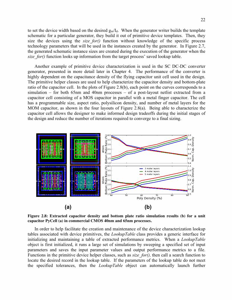
22
to set the device width based on the desired gm/Id. When the generator writer builds the template schematic for a particular generator, they build it out of primitive device templates. Then, they size the devices using the size_for() function without knowledge of the specific process technology parameters that will be used in the instances created by the generator. In Figure 2.7, the generated schematic instance sizes are created during the execution of the generator when the size_for() function looks up information from the target process’ saved lookup table.
Another example of primitive device characterization is used in the SC DC-DC converter generator, presented in more detail later in Chapter 4. The performance of the converter is highly dependent on the capacitance density of the flying capacitor unit cell used in the design. The primitive helper classes are used to help characterize the capacitor density and bottom-plate ratio of the capacitor cell. In the plots of Figure 2.8(b), each point on the curves corresponds to a simulation – for both 65nm and 40nm processes – of a post-layout netlist extracted from a capacitor cell consisting of a MOS capacitor in parallel with a metal finger capacitor. The cell has a programmable size, aspect ratio, polysilicon density, and number of metal layers for the MOM capacitor, as shown in the four layouts of Figure 2.8(a). Being able to characterize the capacitor cell allows the designer to make informed design tradeoffs during the initial stages of the design and reduce the number of iterations required to converge to a final sizing.
Figure 2.8: Extracted capacitor density and bottom plate ratio simulation results (b) for a unit capacitor PyCell (a) in commercial CMOS 40nm and 65nm processes.
In order to help facilitate the creation and maintenance of the device characterization lookup tables associated with device primitives, the LookupTable class provides a generic interface for initializing and maintaining a table of extracted performance metrics. When a LookupTable object is first initialized, it runs a large set of simulations by sweeping a specified set of input parameters and saves the input parameter values and output performance metrics to a file. Functions in the primitive device helper classes, such as size_for(), then call a search function to locate the desired record in the lookup table. If the parameters of the lookup table do not meet the specified tolerances, then the LookupTable object can automatically launch further
�D� �E�
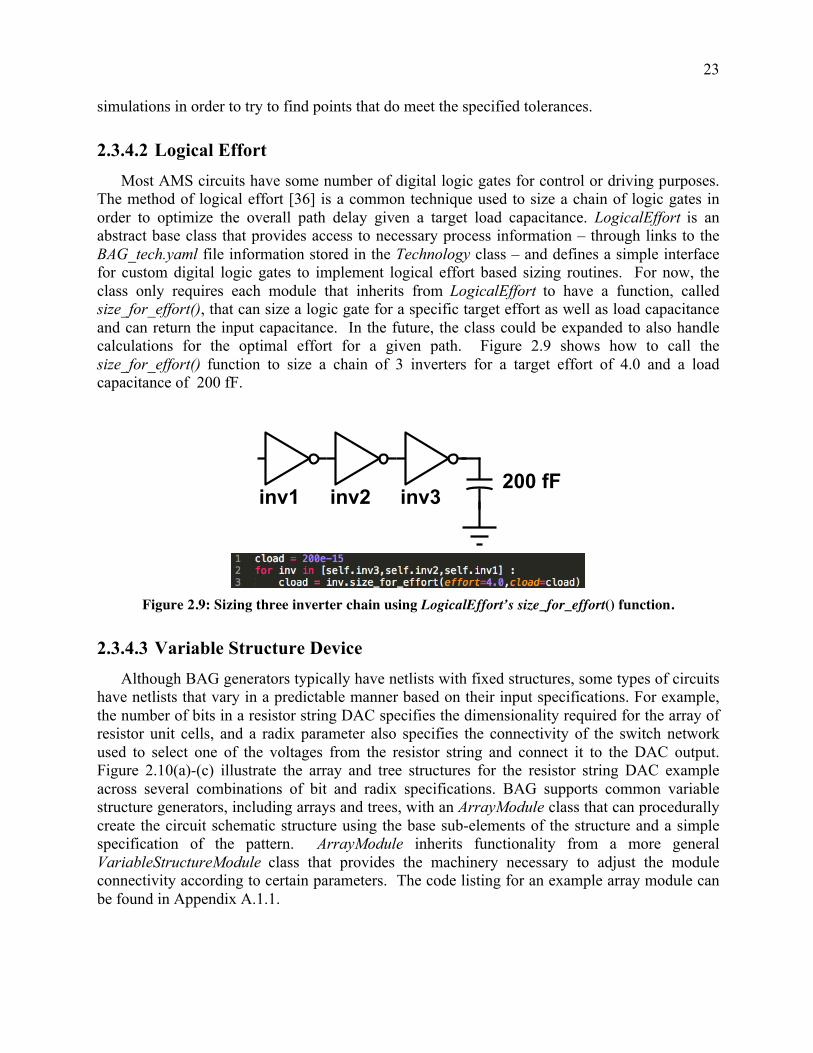
23
simulations in order to try to find points that do meet the specified tolerances.
2.3.4.2 Logical Effort Most AMS circuits have some number of digital logic gates for control or driving purposes.
The method of logical effort [36] is a common technique used to size a chain of logic gates in order to optimize the overall path delay given a target load capacitance. LogicalEffort is an abstract base class that provides access to necessary process information – through links to the BAG_tech.yaml file information stored in the Technology class – and defines a simple interface for custom digital logic gates to implement logical effort based sizing routines. For now, the class only requires each module that inherits from LogicalEffort to have a function, called size_for_effort(), that can size a logic gate for a specific target effort as well as load capacitance and can return the input capacitance. In the future, the class could be expanded to also handle calculations for the optimal effort for a given path. Figure 2.9 shows how to call the size_for_effort() function to size a chain of 3 inverters for a target effort of 4.0 and a load capacitance of 200 fF.
Figure 2.9: Sizing three inverter chain using LogicalEffort’s size_for_effort() function.
2.3.4.3 Variable Structure Device Although BAG generators typically have netlists with fixed structures, some types of circuits
have netlists that vary in a predictable manner based on their input specifications. For example, the number of bits in a resistor string DAC specifies the dimensionality required for the array of resistor unit cells, and a radix parameter also specifies the connectivity of the switch network used to select one of the voltages from the resistor string and connect it to the DAC output. Figure 2.10(a)-(c) illustrate the array and tree structures for the resistor string DAC example across several combinations of bit and radix specifications. BAG supports common variable structure generators, including arrays and trees, with an ArrayModule class that can procedurally create the circuit schematic structure using the base sub-elements of the structure and a simple specification of the pattern. ArrayModule inherits functionality from a more general VariableStructureModule class that provides the machinery necessary to adjust the module connectivity according to certain parameters. The code listing for an example array module can be found in Appendix A.1.1.
����I)LQY� LQY� LQY�

24
Figure 2.10: Three specific instances of a variable structure architecture for a resistor string DAC with bits = 2, radix = 4 (a), bits = 3, radix = 4 (b), and bits = 3, radix = 2 (c).
Each VariableStructureModule object has a set of regular design parameters and a set of parameters that can lead to a structural change called structural parameters. When a structural parameter is changed, it sets the value of an attribute of the module indicating that it requires a structural update. The designer can cause this structural update to happen immediately after the structural parameter value is changed by having the callback function for that structural parameter directly call the update_structure() function. By default, the update_structure() function is not called after every parameter change because that can waste a lot of time especially when the designer sets a large number of structural parameters in one contiguous code block. Instead of updating the structure after each one, it makes more sense to set all of the parameters and then just update the structure once. By default, operations that require an up-to-date netlist call update_structure() directly to make sure that the current circuit netlist matches the value specified by the structural parameters. As an example, the functions that launch simulations call update_structure() before doing any other action.
2.3.4.4 Veriloga When cells have a variable structure, they often need a testbench with a variable structure. A
simple example is a DAC; in order to measure the DNL of a DAC, we need a digital source with a variable number of output bits. One way to implement a source like this is to write some simple veriloga code. The veriloga helper class allows the designer to include veriloga blocks in their testbenches. Note that this class would also be useful in the future to allow simulations to swap out a spice model of a schematic cell with a veriloga model.
2.4 Design Flow Example In this section, the design flow of Figure 2.2 is elucidated through an example design of the
power-gated NOR driver shown in Figure 2.11(a). This design is relevant because it is used as a building block of the DC- DC converter that will be described in Chapter 4. Figure 2.11(b)
9UHI
9UHI 9UHI
�D� �E� �F�
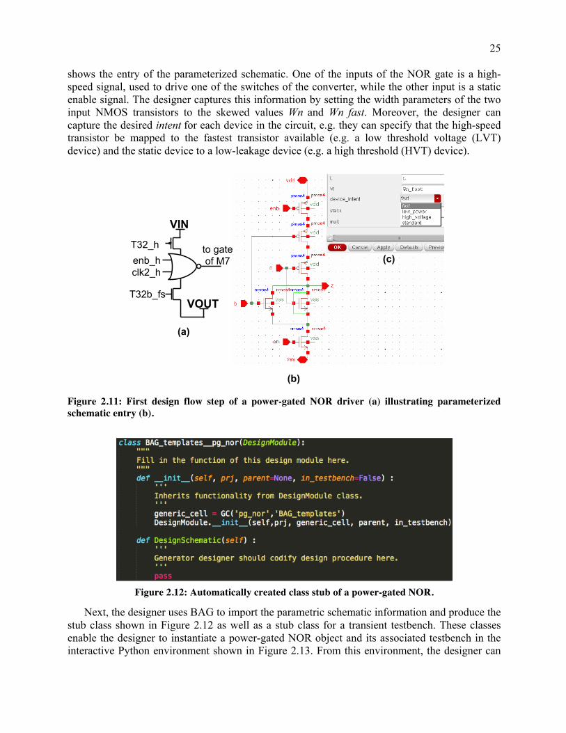
25
shows the entry of the parameterized schematic. One of the inputs of the NOR gate is a high-speed signal, used to drive one of the switches of the converter, while the other input is a static enable signal. The designer captures this information by setting the width parameters of the two input NMOS transistors to the skewed values Wn and Wn fast. Moreover, the designer can capture the desired intent for each device in the circuit, e.g. they can specify that the high-speed transistor be mapped to the fastest transistor available (e.g. a low threshold voltage (LVT) device) and the static device to a low-leakage device (e.g. a high threshold (HVT) device).
Figure 2.11: First design flow step of a power-gated NOR driver (a) illustrating parameterized schematic entry (b).
Figure 2.12: Automatically created class stub of a power-gated NOR.
Next, the designer uses BAG to import the parametric schematic information and produce the stub class shown in Figure 2.12 as well as a stub class for a transient testbench. These classes enable the designer to instantiate a power-gated NOR object and its associated testbench in the interactive Python environment shown in Figure 2.13. From this environment, the designer can
9287
9,17��BK
FON�BKHQEBK
7��EBIV
WR�JDWH�RI�0�
�D�
�E�
�F�

26
access the design hierarchy and parameters using a simple dot syntax – e.g.
pg_nor.NM1.W = desired_width
The designer can then – within the interactive environment – explore the design by choosing an initial sizing, simulating, viewing the results, and adjusting the schematic sizes based on the results.
Figure 2.13: Interactive schematic exploration of a power-gated NOR.
Within the BAG framework, PyCells for custom digital cells – like the skewed, power-gated NOR of this example– can be generated automatically. The netlist information is used to create an intermediate data structure – as shown in Figure 2.14 – that is readable by the Standard Cell layout style described later in Chapter 3 [37].

27
Figure 2.14 : Fully automated PyCell generation of a power gated NOR.
Figure 2.15 shows a PyCell debugging environment provided by Synopsys where the designer can test further changes if needed before incorporating them into the PyCell code. Once an initial PyCell is compiled, the designer can return to the interactive Python environment to run physical verification checks (DRC and LVS), extract layout parasitics, and rerun the testbench simulations (Figure 2.16). The designer now has enough information to implement the methods of the generator interface into the BAG Gated-NOR generator class.
Figure 2.15: Interactive layout exploration using PyCell Explorer.

28
Figure 2.16: Interactive schematic exploration with post-layout extraction.

29
Chapter 3 – Layout As mentioned in the previous chapter, a circuit generator framework must provide a way to
codify all portions of the design process including layout. Unfortunately, analog layout generators are much more difficult to create than digital layout generators. In the digital world, layout generation is typically provided by place and route tools that rely on a functionally complete library of highly regular, easily-composable structures – i.e. digital standard cells – to automatically build hierarchical layouts from a circuit netlist. For analog circuits, the only functionally complete library of structures is the technology library itself. Since the devices in the technology library do not share a common template, they are not easily composable, and the tools for automatically placing and routing them are much more complex than the corresponding digital tools.
3.1 Layout in the BAG Framework The layout portion of the BAG framework, just like the framework as a whole, must be
simple to learn and easy to adapt for new layouts and new processes. Generated layouts should be LVS and DRC correct across most, if not all, of the allowable parameter space. If the designer encounters a corner case where the layout fails to meet DRC or LVS, it must be straightforward to modify the layout generator to fix the error.
Techniques for creating AMS layout generators generally fall into the same two categories as comprehensive circuit generators: optimization-based and knowledge-based. Optimization-based techniques usually require the circuit designer to enter constraints in a special format that is then passed to a tool that automatically places the devices and performs routing. In contrast to knowledge-based techniques, it is not necessary for the designer to write procedures that explicitly create geometric objects. There are several commercially available optimization-based tools for analog placement and routing including Synopsys Helix [38] and Pulsic’s Unity Analog Router [39]. Due to limited time, we have so far focused on just a few knowledge-based techniques and have not included interfaces for these commercial tools yet. However, the intent of the BAG framework is to allow the designer to choose whatever method for creating parametric layouts they want, so interfacing with optimization-based AMS layout tools is on the development roadmap.
Layout generation efforts in the BAG framework have largely focused on knowledge-based techniques for AMS layout built around parameterized cells (Pcells). Pcells are procedures written by layout designers that read in user-specified parameter values and create corresponding geometric objects in the design database of the cell. When writing Pcells, designers must take care to account for all relevant design rules in order to ensure a DRC correct layout. Typically, these are written using Cadence’s proprietary SKILL language, but the OpenAccess database provides a plugin interface so that they can be written in any language including C, TCL, or Python. Pcells are almost universally used for low-level device primitives – e.g. transistors – but avoided for even simple multi-device cells because of the amount of coding effort necessary to make a DRC clean layout.

30
In order to reduce this effort, Ciranova7 introduced PyCells that still directly create geometry, but use functions that automatically check and account for the design rules so that the produced layout is DRC correct by construction. This helps designers create more robust layout generators with much simpler code; in fact, in many cases these generators can be directly compiled for several different processes without changing the code, as shown in Figure 3.1. PyCells do have some disadvantages though, for example large PyCells that do not take advantage of structural repetitions can have long compile times, an anathema to iterative design flows. The generator designer should thus carefully plan the demarcation of hierarchical boundaries and take advantage of the capability of caching the layout of sub-modules if possible.
Figure 3.1: Instances of an amplifier PyCell compiled using a 65nm (a) and 40nm (b) technology file and of a network of power switches and drivers compiled using a 65nm (c) and a 40nm (d) technology file.
7 Now Synopsys.
�D� �E�
�F�
�G�

31
Figure 3.2 shows the three different paths enabled so far for creating layout generators in the BAG framework. All three rely on PyCells, but each requires a different amount of further design effort. For top level and high level cells with complex hierarchies, the designer can create a fully custom PyCell. The BAG framework provides some extra functions beyond the basic PyCell API, but of the three paths, this one certainly requires the most effort from the designer. At the other end of the spectrum, custom digital cell layouts can be fully generated as described in [37].
The contribution of this work is primarily for cells that fit in between these two categories. For AMS cells with only a few levels of hierarchy that fit into one of several categories of common layout styles, the BAG framework provides abstract base PyCells that the designer can use as a base for their PyCell code. These styles provide useful functions for performing common tasks in the layout and can even provide a complete layout procedure so that all the designer must do is enter parameters into a template data structure. Using only a handful of such layout styles, our goal is to provide a quick path to creating DRC/LVS correct layouts so that the designer can quickly begin design iterations including the effects of layout parasitics. Ideally, these layouts can be used with minimal modification, but in the event that they require modification, they are designed to be easy to alter and extend. The remainder of this chapter will focus on the four styles created for the BAG framework so far: Standard Cell, Standard Row, Standard Block, and Array.
Figure 3.2: BAG layout generator flow.
3.2 BAG Standard Styles The Standard family of layout styles – i.e. Standard Cell, Standard Row, and Standard Block – is intended for use as the default layout style for all AMS cells ranging from individual cells like amplifiers, comparators, and level shifters to larger blocks formed from hierarchical
3DUDPHWULF�6FKHPDWLF
&RPPRQ�ORZ�OHYHO�FHOO"
3URFHVV�,QGHSHQGHQW�
3FHOO
<HV 1R
'5&�/96�&OHDQ"
1R
'RQH
$XWRPDWLF�3FHOO
*HQHUDWLRQ
&XVWRP�'LJLWDO�&HOO"
3FHOO�/D\RXW�6W\OH
<HV
1R<HV

32
interconnections of cells. A general style that can handle almost any type of cell is very useful as an initial layout generator so that designers can easily create layouts early on in the generator writing process. This enables the designer to quickly identify and focus on the most important layout parasitics and use that information in the schematic sizing procedure. Beyond providing rapid layout feedback, the goal for the Standard styles is to create high quality layouts so that, for many cells, the initial layout is good enough (i.e. DRC and LVS clean with reasonable parasitics) – freeing the designer from spending any significant amount of time modifying the layout. Standard style cells also have programmable aspect ratios that make them ideally suited for placement around and between other AMS blocks with more rigid layout requirements.
Standard Cell 3.2.1The basic unit of the Standard family of layout styles is the Standard Cell style. Standard
Cell style is used to implement leaf cells, i.e. cells that are built entirely from primitive elements. All of the Standard styles are implemented as abstract PyCell classes that read a data structure entered by the designer and translate it into a layout. The data structure defining Standard Cell layouts, shown in Figure 3.3, consists of Python dictionaries that provide details about the layers and relative locations of power rails, transistor devices, and the cell terminals and internal routing nets. For many cells, creating this data structure is sufficient to produce a DRC and LVS clean layout, however, for more complex cells, the designer must extend or override the functionality of the Standard Cell class.
Figure 3.3: Standard Cell layout style.
Standard Cell PyCells have a number of parameters that allow the designer to control e.g. the vertical pitch of the cell, the width of power rails, the vertical space dedicated to NMOS vs. PMOS devices, whether the cell is in deep nwell or not, the flavors of the devices (LVT, HVT, thick oxide...), whether (and where) to add dummies to each device, whether to add vertical pins
5DLO
'HYLFH�*URXS
'HYLFH�*URXS
5RXWH�*URXS
5DLO

33
on either side of the cell, etc. Figure 3.4 illustrates several of these capabilities for an amplifier circuit; this figure also demonstrates an additional parameter that allows the class to automatically adjust the ratio of vertical space dedicated to NMOS vs. PMOS devices in order to equalize the number of PMOS fingers to the number of NMOS fingers and avoid wasting space. This is illustrated by the reduction of empty space next to the PMOS devices and the overall cell width between Figure 3.4(c) and Figure 3.4(d)-(f).
Figure 3.4: A 5-transistor amplifier PyCell (a) after sequentially lowering the vertical pitch (b), increasing the rail width (c), balancing the NMOS and PMOS ratios (d), adding dummies (e), and increasing the channel length (f).
�D� �E� �F�
�G� �H� �I�

34
The parameters available in Standard Cell PyCells are enabled by a python class that reads in the user-entered data structure and follows a specific procedure to generate a layout instance. This procedure, using the 5-transistor amplifier circuit shown in Figure 3.5 as an example, is as follows:
Figure 3.5: 5-transistor amplifier schematic.
1. Initial Placement – An initial placement of the three main components of all Standard Cells – rails, device groups, and route groups – is made using the order specified in the Python data structure. Placement is done relative to the mason-dixon line – i.e. the line through the middle of a routing group that separates the PMOS device groups (by default in the northern region of the cell) from the NMOS device groups. This initial placement, illustrated in Figure 3.6, makes use of the correct-by-construction PyCell methods to ensure a DRC-clean placement, but does not attempt to meet the vertical pitch constraint, which specifies the distance between the top and bottom rails.
Figure 3.6: Initial placement of a 5-T amplifier in the Standard Cell style.
2. Resizing Loop - A device resizing loop iterates through the devices in each device group and attempts to fit them in the vertical space allocated for that device group (based on
ELDV
LQS LQPWDLO
PLUURU RXW
PDVRQ�GL[RQRXWRXW
3ODFHPHQW�2UGHU
3ODFHPHQW�2UGHU
9HUWLFDO3LWFK
PLUURU
LQS
LQP
WDLO
ELDV
RXW
PLUURU
LQS
LQP
WDLO
ELDV
PLUURU

35
ratios allocated for the PMOS to NMOS regions as well as each device group) by increasing the number of fingers in the device while maintaining a constant (subject to quantization error) device width. As shown in Figure 3.7, the loop completes when the devices have been resized sufficiently that the power rails can be placed such that they meet the cell's vertical pitch constraint.
Figure 3.7: Automatic resizing of device groups in a standard cell in order to fit within the user-specified vertical pitch.
3. Initial Routing - Routing from the devices in each device group to the rails and to the routes in the route group is performed (see Figure 3.9(a)). The current routing mechanism relies on proper net ordering and device ordering in the data structure to avoid shorts. More sophisticated routing algorithms could be incorporated into the Standard Cell style in the future in order to simplify and/or improve the routing.
4. Routing Repair – The initial routing is not necessarily free of DRC errors so a cleanup step is performed that can repair certain types of DRC errors such as those created when devices from above and below connect routes to the same horizontal net and cause minimum spacing errors as shown in Figure 3.8(a). Drawing a rectangle to fill in the minimum spacing region can repair this. Also, if the contacts associated with the two routes are too close, the routing repair step simply removes one of the contacts. Another problem fixed during the repair step is associated with vertical routes from above and below connecting to adjacent horizontal nets, as shown in Figure 3.8(b). In order to repair this DRC error, the internal spacing between the horizontal nets is automatically increased, and steps 3 through 4 are rerun.
'5&�(UURU
'5&�(UURU
PDVRQ�GL[RQRXW
PLUURU
LQS
LQP
WDLO
ELDV
RXW
PLUURU
LQS
LQP
WDLO
ELDV
9HUWLFDO3LWFK

36
Figure 3.8: Two DRC errors and their associated fixes performed during the routing repair step.
5. Routing Finalization - The cell is finalized by trimming excess material from routes, creating pins, and adding/modifying enclosing layers as shown in Figure 3.9(b).
Figure 3.9: 5-transistor amplifier layout after initial routing (a) and routing finalization (b).
Standard Row 3.2.2The power of the Standard family of layout styles is fully realized when several Standard
Cells are connected together in such a way that the interconnected block still retains its programmability, especially the flexible aspect ratio. There are two styles in the BAG framework that enable the interconnection of Standard Cells. The simpler of these, the Standard Row style shown in Figure 3.10, is used to connect a row of Standard Cells if their inputs and outputs are connected only to adjacent cells. The cells and the route groups used to connect them are placed following the order specified in a data structure that the layout designer creates in the PyCell file. An example PyCell that uses the Standard Row style can be found in Appendix A.2.2.
�D� �E�
RXW
PLUURU
LQS
LQP
WDLO
ELDV
RXW
PLUURU
LQS
LQP
WDLO
ELDV
�D� �E�

37
Figure 3.10: Standard Row style cell.
Standard Block 3.2.3Standard Row is useful for small groups of Standard Cells with simple connectivity, but for
more complex hierarchical blocks, fully specifying the routing can be challenging due to the limitations imposed by the Standard Row route groups and by the potentially large number of routes. Also, because Standard Row layouts are limited to a single row of cells, it can be difficult to enable a flexible aspect ratio when the number of cells in the row becomes large. To enable larger hierarchical blocks, the Standard Block style, illustrated in Figure 3.11, has the capability to stack rows of Standard Cells (or Standard Row objects), includes a more flexible semi-automated routing mechanism as well as a function for creating a simple power grid. An example code listing for a Standard Block cell can be found in Appendix A.2.4.
Figure 3.11 Standard Block style.
5RXWH�*URXS
5RXWH�*URXS
6WG�&HOO
6WG�&HOO
6WG�&HOO
*1'9
''
9''
*1'
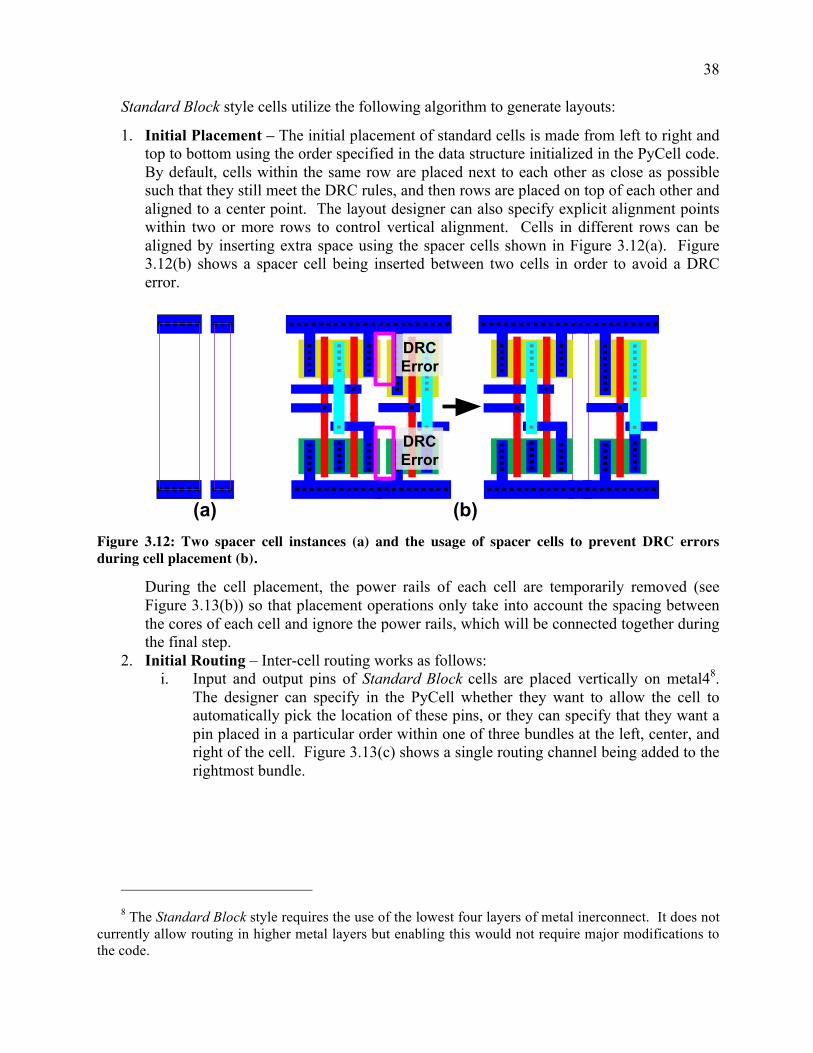
38
Standard Block style cells utilize the following algorithm to generate layouts:
1. Initial Placement – The initial placement of standard cells is made from left to right and top to bottom using the order specified in the data structure initialized in the PyCell code. By default, cells within the same row are placed next to each other as close as possible such that they still meet the DRC rules, and then rows are placed on top of each other and aligned to a center point. The layout designer can also specify explicit alignment points within two or more rows to control vertical alignment. Cells in different rows can be aligned by inserting extra space using the spacer cells shown in Figure 3.12(a). Figure 3.12(b) shows a spacer cell being inserted between two cells in order to avoid a DRC error.
Figure 3.12: Two spacer cell instances (a) and the usage of spacer cells to prevent DRC errors during cell placement (b).
During the cell placement, the power rails of each cell are temporarily removed (see Figure 3.13(b)) so that placement operations only take into account the spacing between the cores of each cell and ignore the power rails, which will be connected together during the final step.
2. Initial Routing – Inter-cell routing works as follows: i. Input and output pins of Standard Block cells are placed vertically on metal48.
The designer can specify in the PyCell whether they want to allow the cell to automatically pick the location of these pins, or they can specify that they want a pin placed in a particular order within one of three bundles at the left, center, and right of the cell. Figure 3.13(c) shows a single routing channel being added to the rightmost bundle.
8 The Standard Block style requires the use of the lowest four layers of metal inerconnect. It does not
currently allow routing in higher metal layers but enabling this would not require major modifications to the code.
�D� �E�
'5&(UURU
'5&(UURU

39
Figure 3.13: A Standard Block cell after initial placement with (a) and without (b) power rails and the same cell after the first routing step where a single vertical routing channel has been placed in the rightmost bundle.
ii. After the bundles are created, all the remaining nets that are connected to a top level pin are assigned to a free vertical routing channel from left to right in the order specified by the designer, as shown in Figure 3.14(a).
iii. Horizontal routing channels are assigned within each row for every net in the row (see Figure 3.14(b)). If the locations of the vertical routes associated with the horizontal route are known, then the horizontal route can be limited to a particular region, freeing up that horizontal routing channel for other routes. If not, by default, the entire length of the cell is temporarily dedicated to a single net.
iv. Vertical routing channels for any remaining nets that are shared between rows are placed on the x-axis as shown in Figure 3.14(c). The position of each vertical route is chosen so that the final length of interconnect required for the net will be minimized once the excess metal is trimmed from the horizontal routes in the cell finishing step.
Figure 3.14: During the initial routing phase a Standard Block cell has all top level pins assigned to a vertical channel (a), has horizontal channels assigned to all intra-row nets (b), and then has a vertical channel assigned for any inter-row nets (c).
3. Power Grid – A simple power grid is created according to the power grid specification in the PyCell code. The specification sets a pattern for power rails and a target width and spacing. If the spacing cannot be met because of existing routing channels, the power rail is placed in the next available routing channel as shown in Figure 3.15(a). The power grid step can be run before the initial routing if the designer desires a more regular grid.
�D� �E� �F�
�D� �E� �F�

40
4. Final Routing – Given the location of all the vertical routes at the higher and lower metal levels, the horizontal routes can now be reorganized within the horizontal routing channels to minimize the length of each net and minimize the total number of horizontal routing channels required (see Figure 3.15(b)).
5. Cell Finishing – The power rails for each of the Standard Cells, removed during the initial placement, are added back in on a row-by-row basis and are strapped up to metal3 and connected to the power grid on metal4 (see Figure 3.15(c)). Excess material from routes and power grid rails is also removed in order to minimize parasitic coupling but it can be added back in by a higher level PyCell if it is needed for connectivity or to connect the power grid of two cells.
Figure 3.15: A Standard Block cell is finalized by adding a power grid (a), trimming and reorganizing routes (b), and rerouting the power rails on each row (c).
3.3 BAG Array Style The repeated patterns that appear in the schematics of the variable tree structures described in
2.3.4.3 also appear in the layouts of those cells. BAG includes a layout Array style to simplify the creation of PyCells for cells constructed by repeatedly placing a handful of unit elements in a grid pattern. Figure 3.16 shows a floorplan of such a cell where an array of unit cells is connected using a common-centroid pattern. The style also includes provisions for inserting additional cells for auxiliary purposes - e.g., biasing and/or dummy cells.
9''
9''
*1'
*1'
9''
9''
*1'
*1'
*1'9
''
9''
*1'
�D� �E� �F�

41
Figure 3.16: Array style floorplan of top level array and example layout of a unit cell.
Implementing a layout in the Array style involves two PyCells: the top-level array PyCell which should inherit from the Array style class, and the unit cell PyCell which can be a fully custom PyCell, or can inherit from another style class such as Standard Cell. The top-level array PyCell has parameters to adjust the number of cells (or number of bits) in the array, the unit cell placement pattern, the symmetry of adjacent cells, and the number as well as the arrangement of auxiliary cells. It also helps route control signals at the edges of the array.
The unit cell PyCell can use any style the designer wants, but must adhere to a few basic rules in order to function properly when it is instantiated by a top level array cell. First, it should be DRC correct when abutted on any side to other unit cells on its cell boundary. Also, as shown in Figure 3.17, it should have a parameter that can be used to control whether it is a regular unit cell, a dummy cell, or some other auxiliary cell like a bias cell. If it is difficult to write a single unit PyCell that can create all the different auxiliary cells, then separate PyCells for each type of auxiliary cell can be wrapped by a higher level PyCell which can then be used as the unit cell of an array.
Figure 3.17: Using only the highlighted vias and stiches, a unit cell (a) can be configured for control by an odd bit (b), control by an even bit (c), or configured as a dummy cell (d).
Figure 3.18 shows three instances of a programmable array for two, three, and four bits of programmability. These instances use the default placement pattern of binary-weighted cells for Array Style cells. The main benefit of this pattern is that it only uses one horizontal and one vertical routing channel per control bit no matter how many bits are in the array. Even numbered control bits (as shown in Figure 3.17(c)) are routed to the left edge of the array horizontally and odd numbered control bits (as shown in Figure 3.17 (b)) are routed to the top vertically. If this pattern is not suitable for a particular application, the designer can select another placement pattern or can create their own.
%'HYLFHV
5RXWLQJ�&KDQQHOV
%%
'XPP\�&HOO
%LDV�&HOO
�D� �E� �F� �G�

42
Figure 3.18: Three instances of binary weighted DACs 2, 3, and 4 bits.
3.4 Summary An AMS circuit generator is not complete unless it can generate a full layout. There are
commercially available tools for automating the creation of analog circuit layouts, but they have not yet seen widespread adoption by designers. We believe the main complaint designers have with these tools – most of which are optimization-based tools – is the difficulty in creating constraints that can help the tool perform a layout in a way that is similar to the way the designer would manually layout the circuit. Some readers might rightly point out that manual layout techniques can be non-optimal and might include unnecessary levels of symmetry or possess other aesthetically pleasing but electrically irrelevant properties. While this may be true and the layout produced by an optimization-based AMS layout tool might actually match – or even exceed – the performance of a manual layout, it is also true that it is much easier for a designer to debug a layout when they are familiar with it and understand the details of how it was created9. Constraint-driven optimization tools can often lead to non-intuitive results, leading to extra time spent adding extra constraints in order to force the tool to behave as the designer wishes.
Due to these issues with existing constraint-based approaches, the initial efforts towards enabling designers to easily create layout generators using the BAG framework have primarily focused on knowledge-based techniques that allow designers to fully specify the procedure for building a parameterized layout. Naturally, these layouts match more closely with the designer’s plan but codifying a complex circuit can require many lines of code and a lot of time. To mitigate these issues, we created several Python classes that designers can use as the basis for building their own PyCell layout generators for a few common styles of AMS circuits. It is our
9 It is also important to recognize that designers have an inherent bias to trust the layout they personally envisioned more than one created by something (or someone) else. This isn’t a particularly justifiable or defensible bias but it is a reality that must be addressed.
� �� ' � �
� '� �
� �� �� '� �
� ����
����
�

43
hope that using just a handful of these layout styles, the BAG framework can provide a quick path for creating layout generators for 90% of the circuit generators created using the framework.
The main styles of the BAG framework are the Standard styles: Standard Cell, Standard Row, and Standard Block. These styles allow the designer to enter a design in a simple Python data structure wherein the order of elements in the data structure corresponds to the relative placement of the elements in the layout. They are also general enough to use for almost any circuit so they are useful for creating initial layout generators to provide accurate layout parasitic estimates early on in the design process. The Standard styles can be used for cells made of device primitives and/or groups of dissimilar cells; the Array style is used to create regular layouts for groups of a single unit cell. When combined with a unit cell layout built from the Standard Cell style, this can be used to build DAC and ADC structures and other regular arrays.

44
Chapter 4 – Integrated SC Regulator The previous 2 chapters have described the functionality of the BAG framework using only
simple example circuits such as basic digital gates and a 5-transistor amplifier. In order to demonstrate the true utility of an analog circuit automation framework, it must be used to create generators for more complex circuit blocks. The most complex circuit generator created using BAG so far is a fully-integrated Switched-Capacitor (SC) regulator. This chapter begins with some brief background on the operation of switched-capacitor converters before moving to a description of a fully-integrated switched-capacitor regulator architecture capable of responding to sub-nanosecond load current transients. The main topics of this chapter are a description of both the generator and the process of creating the generator for this switched-capacitor regulator architecture.
4.1 Switched-capacitor Converters As the number of digital cores and peripheral blocks with separate voltage supplies in
modern SoCs increases, integrated voltage regulators (IVRs) are becoming increasingly desirable as a means of providing multiple voltage supplies without requiring costly external components. Since a typical chip requires several independent supplies with different output voltage and efficiency requirements, the initial design effort spent creating an IVR generator can be immediately amortized across several instances. Furthermore, as IVRs are needed all over the SoC, having a layout with a programmable aspect ratio can help ease floor-planning by allowing the designer to fill in arbitrarily-shaped spaces on the die. IVRs do not typically have many critical, high speed input/output signals, so it is also useful to be able to adapt their shape to accommodate placement and routing constraints imposed by more critical high speed blocks such as transceivers or data paths.
Low-dropout regulators (LDOs) are a common choice for integrated voltage regulators, but their efficiency scales linearly with their conversion ratio (i.e. the ratio of the converter’s output voltage to its input voltage), and in many cases this inefficiency is unacceptable. In order to achieve higher efficiencies, designers use switching regulators. The buck converter is probably the most popular step-down converter used for efficient power conversion, but it relies on high quality inductors, which are difficult to integrate on chip in a cost effective way. Switched-capacitor converters [40] rely on dense capacitors rather than high quality inductors, generally making them more well-suited to complete integration on the die.
Switched-Capacitor DC-DC Converter Operation 4.1.1The basic operation of a simple two-to-one step-down – i.e. having an ideal voltage
conversion ratio of ½ – switched-capacitor converter is depicted in Figure 4.1(a). Two non-overlapped clocks, Phase 1 and Phase 2, control a group of switches that alternately shift a capacitor, called the flying capacitor, from being connected between an input and an output voltage to being connected between the output voltage and ground. While this switching action delivers power from the input to the output at the desired conversion ratio, it also creates an undesirable ripple voltage shown on the Vout waveform at the bottom of Figure 4.1(a). The loss

45
in system efficiency associated with this ripple can be improved by interleaving several of the switched-capacitor units. Figure 4.1(b) illustrates interleaving with two flying capacitors 90 degrees out of phase with each other. The number of interleaved phases along with the topology of the SC converter, frequency of switching, size of the flying capacitors, and size of the switches determine the exact relationship of the output voltage to the input voltage and the efficiency of the power conversion. For a more thorough analysis of switched-capacitor DC-DC converters, see [41].
Figure 4.1: Switched-capacitor Operation.
When controlled by a fixed frequency, as in Figure 4.1, a switched-capacitor converter does not truly regulate the output voltage. In order to create a regulated switched-capacitor converter (i.e., a switched-capacitor regulator), the frequency of the flying capacitor switching action must be controlled through a closed loop that compares the output voltage to a desired reference voltage. One way of doing this is by using a lower-bound hysteretic feedback controller shown in Figure 4.2 [42]. The lower-bound comparator detects when the output voltage drops below the reference and triggers a flip in the state of the switched-capacitor switch network. This action regulates the output voltage to the desired value despite changes in input voltage or load current such as the current steps in Figure 4.2(c).
3KDVH��3KDVH��E
�E��D�
9RXW
,QWHUOHDYLQJ
9RXW
&IO\
0� 0�
0� 0�
9LQ
&IO\
0� 0�
0� 0�
9LQ
9RXW
&IO\
0� 0�
0� 0�
9LQ
3KDVH��3KDVH��E3KDVH��
3KDVH��E

46
Figure 4.2: A lower bound hysteretic control circuit (a) used to control a switched-capacitor converter unit cell (b) and the waveforms (c) depicting its operation.
Switched-Capacitor Regulator Architecture 4.1.2Since fully integrated SC converters are physically close to their loads and have fewer
inductive and capacitive parasitics to deal with, they can inherently be made to respond faster than off-chip converters. If an integrated convert’s regulation loop can fully capitalize on this capability, it can be used to enable fast dynamic voltage and frequency scaling (DVFS) which can lead to substantial power savings [43]. For this reason, creating regulation schemes that achieve very fast response times is an open and worthwhile challenge. Therefore, we chose to implement (using BAG) a generator for a switched-capacitor regulator that extends the work of [40]–[42] with a very fast response time that can maintain output regulation in the presence of sub-nanosecond load current transients.
SC converters have an inherent voltage conversion ratio determined by their topology. Unfortunately, as a regulation loop adjusts the output voltage and the effective conversion ratio shifts below the inherent ratio of the topology, the efficiency of the converter drops linearly. In order to mitigate this, the architecture chosen for the SC regulator generator uses a reconfigurable switched-capacitor unit cell [41] that can switch between 1/2 to 2/3 conversion ratios. This allows the converter to be reconfigured for higher efficiency depending on the desired conversion ratio. The regulation loop used to control the reconfigurable unit cells is similar to the lower bound control shown in the previous section, but modified to handle multi-phase interleaving and to maintain a loop response time that is as fast as possible. Each phase has a separate asynchronous comparator that triggers a flip in the state of that phases’ switched-capacitor unit cell as soon as the output voltage drops below the desired reference. Once the output voltage has increased as a result of that flip in the switched-capacitor unit cell’s state, the next comparator in the chain is enabled.
By having a comparator located locally within each phase, the critical path from the comparator to its associated switched-capacitor unit cell is minimized. This is crucial to
9UHI9RXW
4ࡄ4
' 3KDVH��9UHI
9R
��
FON
1RQ�2YHUODS�&ON�*HQHUDWRU
9RXW
&IO\
0� 0�
0� 0�
9LQ
3KDVH��E
3KDVH��3KDVH��E
, ORDG
, ORDG
�D�
�E�
�F�

47
maintaining a fast response to transient load current steps because the maximum switching frequency of the converter, and therefore the maximum load current that the converter can supply while still maintaining output voltage regulation, is limited by this critical path delay.
Figure 4.3: Implemented SC Converter regulation loop with asynchronous lower bound control and its behavior in the presence of a load current step.
4.2 Switched-Capacitor Regulator Generator As highlighted in Figure 4.4, an SC regulator instance is made of an even number of
interleaved phases (the exact number is determined at optimization time) and a corresponding number of bias current DACs. Each of the interleaved phases is itself made of four parts: a collection of flying capacitors, a network of power switches and drivers, a control core, and a load current DAC.
(Q�(Q�(Q�(Q�(Q�(Q�
9UHI9RXW
/RDG�&XUUHQW
4ࡄ4
'4ࡄ4
'
3KDVH�� 3KDVH�� 3KDVH��
9UHI
9RHQ�
��
��
9UHI
9R
4ࡄ4
'
��
9UHI
9RHQ� HQ�

48
Figure 4.4: Switched-capacitor Regulator Generator.
In order to fully validate the functionality and flexibility of the BAG framework and to verify the quality of the resulting circuits, we utilized the SC regulator generator to create three different instantiations, each targeting different specifications in terms of total output power, power density, and aspect ratio, as shown in Table 4.1. The following section will describe the creation of a BAG generator for the regulator as well as the creation of generators for the main sub-blocks utilized by the regulator.
Specification Regulator A Regulator B Regulator C Power Density 1 𝑊 𝑚𝑚! 0.2 𝑊 𝑚𝑚! 1 𝑊 𝑚𝑚! Output Power 1 𝑊 100 𝑚𝑊 100 𝑚𝑊 Aspect Ratio [H/W] 0.35 1.2 0.5
Table 4.1: Switched-capacitor Regulator Target Specifications.
Sub-Circuit Generators 4.2.1We created generators for each sub-block in a bottom-up fashion so that during the
development of the higher-level generators, the lower level generators would be available to instantiate the sub-blocks. However, during the execution of a generator, the specifications are typically passed top-down to each sub-block in order to optimize global performance – e.g. to create as compact of a layout as possible.
4.2.1.1 SC Interleaved Phase Generator Each interleaved phase is made of two out-of-phase reconfigurable switched-capacitor
circuits consisting of two flying capacitors and nine switches along with their drivers. Each phase also has a control block that creates the signals used as inputs to the switch drivers. The generator code for sizing this circuit is trivial because the higher level SC regulator generator handles its sizing. The layout generator is a fully custom PyCell and does not use a specific layout style. The PyCell’s main actions are wrapping the capacitor around the edges of the
6&�&RQYHUWHU�,QWHUOHDYHG�3KDVH
)O\LQJ�&DSDFLWRU
6ZLWFK�1HWZRUN
'HVLJQ0RGXOH
$JJUHJDWLRQ��³KDV�D´�
&RQWURO�&RUH
6&�&RQYHUWHU�
����������1
/RDG�'$&
%LDV�'$&
����������1

49
control block and switch network, creating routing channels between the capacitors to carry static control signals and the comparator enable signal, and driving the switch network and control block PyCells to fit in the targeted space.
Figure 4.5: SC Interleaved Phase schematic (a) and layout (b).
4.2.1.2 Control Core Generator The control core circuit’s main function is to decide when to switch the state of the switched-
capacitor unit cell. To that end, it contains an asynchronous comparator whose output drives a toggle flop followed by a phase splitter that outputs two 180° out-of-phase signals. These out-of-phase signals are then fed to a circuit that creates non-overlapping versions in two voltage domains – between Vin and Vout and between Vout and ground – in order to supply the control signals to the power switch driver circuits in the SC interleaved phase unit cell. The delay from the enable signal of the comparator until the time at which the output voltage is boosted from the charge added in by the switched-capacitor unit represents the fastest speed the converter can maintain regulation. Minimizing the delay of the critical path shown in Figure 4.6 is equivalent to maximizing the allowable switching frequency of the converter and is directly related to the achievable output power. This delay also limits the speed that the regulation loop can respond to changes in the output load.
The primary goal of the control core generator is to minimize the critical path delay. Sizing is done using the logical effort helper class (see 2.3.4.2) to size the elements of the critical path. First, the asynchronous comparator is sized for minimal power and a specified minimum delay. Then, using the driver size specifications passed down from the SC interleaved cell generator, the optimal fanout target is calculated and used to size the rest of the critical path. The falling edge detector is sized to prevent a race condition that can occur if a comparator is enabled before the output voltage has jumped due to the signal from a previous comparators output. In addition to the critical path, the control core generator also sizes measurement circuits that can be used to
�D� ][jg]Y
9RXW9LQ
9LQ
9RXW 9LQ
9LQ
&� &�
&� &�
&�
&�
&�
&�
�E�

50
characterize each interleaved phase, circuitry for resetting the asynchronous comparator once the next phase’s comparator has been enabled, and circuitry for modifying the effective reference voltage depending on the output load.
Figure 4.6: Control core critical path.
The generator of the control core layout inherits from the Standard Block class (see 3.2.3), and all of the subcircuits used in the control core inherit from either Standard Row or Standard Cell. Figure 4.7 shows asynchronous comparator instances implemented using Standard Row. These layouts use a feature of the Standard styles that allows the designer to create isolated power islands using deep nwell regions and breaks in the power rails.
Figure 4.7: Asynchronous comparator PyCell compiled with 65nm and 40nm technology files.
An instance of the layout generator for the full implemented control core can be seen in Figure 4.8. The asynchronous comparator is highlighted in the bottom left of the figure to provide a sense of scale. The top three rows contain the non-overlap and level shift circuitry for the two phases of unit switched-capacitor cells. Their layouts are roughly mirror symmetric
'
1RQRYHUODS/HYHO�6KLIW
3KDVH�6SOLWWHU
9RXW
9UHI
4'
��
1RQRYHUODS/HYHO�6KLIW
8QLW�&DS&HOO���
(Q�)DOOLQJ(GJH�
'HWHFWRU
4
��
(Q�
1RQRYHUODS/HYHO�6KLIW
1RQRYHUODS/HYHO�6KLIW
)DOOLQJ(GJH�
'HWHFWRU
&/.�B+
8QLW�&DS&HOO���
&/.�&/.�B+&/.�
&/.�%B+&/.�%
&/.�%B+&/.�%
8QLW�&DS&HOO���
8QLW�&DS&HOO���
���QP
���QP
'HFRXSOLQJ�&DSDFLWRUV
/DWFKLQJ�(OHPHQW
5HIHUHQFH�(OHPHQW
2XWSXW�%XIIHUV

51
about the center of the y-axis in order to avoid mismatch. Control signals that interface with one SC cell or the other are placed in the left and right routing bundles while signals used for the asynchronous comparator and the shared portion of the control path are placed in the central routing bundle. The vertical portion of the power grid (thick yellow routes) is placed after the routing with extra spacing allocated to avoid adding extra load capacitance to any high speed signals. The power grid rails are also trimmed to avoid extra load capacitance, but this can be disabled with a parameter if a higher level PyCell needs the power grid to reach the borders of the cell.
Figure 4.8: Control Block PyCell.
4.2.1.3 Switch Network Generator The switch network circuit, shown in Figure 4.9, consists of all of the power switches used in
the SC converter as well as the first stage of digital logic driving the gates of the power switches. In order to enable decreased gate switching losses under light load conditions, the power switches are partitioned into 4 equal segments, each controlled by a separate driver. The power switches are sized based on the results of a high level optimization script, and the gate capacitors of these switches are used to size the driver gates for an optimal target effort. This target effort is passed from the higher level SC interleaved phase generator that has information about the entire critical path (and not just the final stage).
$V\QFKURQRXV�&RPSDUDWRU
5RXWLQJ�%XQGOHV

52
Figure 4.9: Power switches and drivers.
The layout of the switch network could be implemented using the Standard Block style, but we chose to implement it as a custom PyCell in order to ensure a compact layout and to avoid potential electromigration issues. Each partitioned switch is implemented as a PyCell like the one shown in Figure 4.10(a) in order to limit the finger width of the switches and maintain a strong connection to the gate. The drivers for most of the switches are NOR and NAND gates created using the Standard Cell layout style. In order to enable the switch network to reconfigure from a conversion ratio of 1/2 to 2/3, two of the switches, M5 and M7, require more complex drivers (see the M7 driver schematic in Figure 4.10(b)). As shown in Figure 4.11(d), the M5 driver has twice the vertical pitch of the other cells. Therefore, in order to avoid potential electromigration issues due to excessively large finger widths, its layout is implemented using the Standard Block style, as shown in Figure 4.10(c), to connect several vertically stacked copies of a unit element of the M5 driver in parallel.
Another challenge for the switch network layout is the need to deal with multiple voltage domains. It is difficult to handle the isolated pwells and deep nwell boundaries used to create separate voltage domains in a way that can easily scale with different switch widths, driver sizes, and target aspect ratios. The relative locations of the switch/driver groups were chosen to minimize the total number of deep nwell regions required in order to minimize the penalty that results from the large minimum spacing requirement associated with the deep nwell layer.
0��GULYHU
9RXW
9LQ0�
0�0
�
0�
0��GULYHU
9RXW
9LQ0�
0�0
�
0�
0��GULYHU
9RXW
9LQ0�
0�0
�
0�
9LQ
9RXW0�
0�0
�
0�
9LQ
9RXW0�
0�0
�
0�
9LQ
9RXW0�
0�0
�
0�
0��GULYHU
9LQ
9RXW0� 0�0� 0�
0��GULYHU
9RXW
9LQ0� 0�0� 0�
&/.�B+
&/.�
&/.�B+
&/.�
&/.�B+
&/.�
&/.�B+
&/.�
&/.�B+ 0�

53
Figure 4.10: Power switch PyCell (a), M7 driver schematic (b), and M5 driver PyCell (c).
The top level layout procedure of the switches and drivers is designed to minimize the amount of empty space in the layout. Using the programmable vertical pitch capability of the driver PyCells and switch PyCell, the bottom row of switches and drivers shown in Figure 4.11 (a) is first placed with a target width set to meet electro-migration specifications. Then a binary search is performed on the pitch of the top row (Figure 4.11(a)-(c)) to match the width of the bottom row. Performing the binary search on the width of the top row while fixing the bottom row is slightly faster than the alternative due to the slower layout generation time of the bottom row resulting from the added complexity of the M7 driver compared to the drivers in the top row. Finally the M5 driver and switch are placed on the left side of the two rows with a vertical pitch set equal to the total height of the two rows (Figure 4.11(d)). This compact layout (see Figure 4.11(e)) would have been hard to obtain using an optimization-based layout generator without specifying a very large number of constraints.
92870�
9,17��BK
FON�BK
HQEBK
7��EBIV
&�BSRV
�D� �E� �F�

54
Figure 4.11: A binary search matches the width of the top row of power switches and drivers with the bottom row (a)-(c) before the final M5 switch placed (d). The actual layout is overlaid by the cartoon in (e).
4.2.1.4 Flying Capacitor Generator The efficiency that a SC converter can achieve for a particular power density is strongly
dependent on the density of the flying capacitors. In order to achieve the densest possible capacitor layout, a PyCell was created covering a MOS capacitor with a programmable number of layers of metal finger capacitors. Since the achievable capacitor density is crucial to the optimization of the overall circuit, this PyCell is characterized early on in the generator’s design procedures (as described in 2.3.4.1) so that the sizes of the switches and capacitors can be determined before laying out the full converter.
One of the main constraints on the achievable capacitor density is the polysilicon maximum density design rule. In order to achieve the absolute highest density possible, once the full converter PyCell is ready, the density of the MOS capacitor in the flying capacitor PyCell can be optimized using a binary search for the highest density such that the full converter meets the maximum polysilicon density design rule.
4.2.1.5 DAC Generators The SC converter uses two different DAC generators for calibration and testing purposes.
Both generators use the ArrayModule class described in 2.3.4.3 to enable the variable structure
0� 0� 0� 0�
0� 0� 0� 0�
0�
0� 0� 0� 0�
0� 0� 0� 0�
0� 0� 0� 0�
0� 0� 0� 0�
0� 0� 0� 0�
0� 0� 0� 0�
0�
0� 0� 0�
0� 0� 0� 0�
0�
0�
0� 0� 0� 0�
0� 0� 0� 0�
�D�
�E�
�F� �G�
�H�
1026�VZLWFKHV3026�VZLWFKHV'ULYHUV

55
schematic required to generate a DAC with a variable number of bits. They also both use the Array style PyCell class described in 3.3 to simplify the layout procedure.
4.2.1.5.1 Bias Current DAC The bias current DAC is used to calibrate the asynchronous comparators in the control block.
It needs to be able to provide the proper current to reduce the offset of the comparator to a few mV. Once the asynchronous comparator is sized, the nominal required current can be calculated through simulation; the bias DAC is then sized (using the size_for() function described in 2.3.4.1) in order to provide that nominal bias current at the worst-case process corner when programmed with a digital value that is one half of its full scale value. The LSB size, and therefore the number of bits required for the bias DAC, is chosen to be small enough to limit the offset due to the step size to be less than a few mV.
The schematics and layouts for the three unit cells used by the Array style bias DAC PyCell are shown in Figure 4.12. The core of the unit cell uses the Standard Cell style and then vertical and horizontal routing channels are added on top of it and connected using programmable vias that transform the cell into a current source element, a mirror bias cell, or a dummy cell. The routing channels also include ground shields for the bias and output lines and are designed to be abutted with or without mirroring across the y-axis.
Figure 4.12: Bias DAC unit elements configured as a basic unit cell, a bias cell, and a dummy cell.
There are no high speed signal paths or high current wires in this design so the default configuration of the Array style is sufficient for the bias current DAC PyCell. The unit cells from Figure 4.12 are used to build the full array PyCell instances shown in Figure 4.13.
HQ
RXWELDV
HQ
HQ
RXWELDV
HQ
HQ
RXWELDV
HQ
%$6,&�&(// %,$6�&(// '800<�&(//

56
Figure 4.13: Bias Current DAC layout instances for 2 and 4 bit configurations.
4.2.1.5.2 Load DAC The benefits of fully integrated SC regulators, and in particular the speed of the transient load
response, are maximized if the load circuit they are supplying is located on the same die. The parasitic inductance incurred when routing power off the die, through the package, and to a load circuit often precludes the sub-nanosecond response time that is one of the goals of this SC regulator. In order to mimic the fast switching transients of a processor core, a dummy load DAC is integrated with each interleaved phase of the regulator. The schematic of the load itself is quite simple; as illustrated in Figure 4.14, it is just an array of unit-sized NMOS devices controlled by a binary-weighted digital code and connected between the power rails. In order to demonstrate the speed of the SC converter, it is useful to have the capability to adjust the speed of the transient load steps. In order to do this, the gates of the NMOS load devices are driven by a set of current-starved inverters whose bias current is digitally programmed using instances of the bias DAC shown previously. The DAC is sized to supply the maximum load current at the peak output voltage specification (1.2 V) under nominal conditions.
'800,(6
'
� �%� '
%
'
%
'
�
�
'
�
�
�
�
�
�
�
�
�
�
�
�
�
%���ELDV'���GXPP\����FRQWURO�ELW
'800,(6

57
Figure 4.14: Load DAC array and slew rate limiter schematics.
The major design considerations for the load DAC are electromigration and thermal power dissipation. Long channel devices are used to decrease the power density of the load DAC and the DAC itself is distributed with the interleaved phase cells such that each interleaved phase has a single copy of the load DAC. The power rails are also upsized to avoid electromigration problems. Figure 4.15 shows the schematic and layout for the unit cells used in the load array. As described earlier in 3.3, the basic Array style pattern dictates that the control signals for even bits are routed to the borders of the array horizontally and for odd bits are routed vertically.
Figure 4.15: Load DAC unit elements configured as a basic unit cell (with an even or odd control bit) and a dummy cell.
Figure 4.16 shows one of the actual load DAC layouts generated for one of the top level converters. A simple wrapper PyCell is created to place the slew rate limiter above the load DAC and connect the routes between them. The power nets of both circuits are connected to the top level power grid later when the load DAC PyCell is instantiated in the SC interleaved phase PyCell.
9287
�1��
9287
SELDV
QELDV
&/.�
� � �1��6/(:�5$7(�
/,0,7(5
/2$'�$55$<
&/.� &/.1
HQ
%$6,&�&(// '800<�&(//
HQ
(9(1 2''
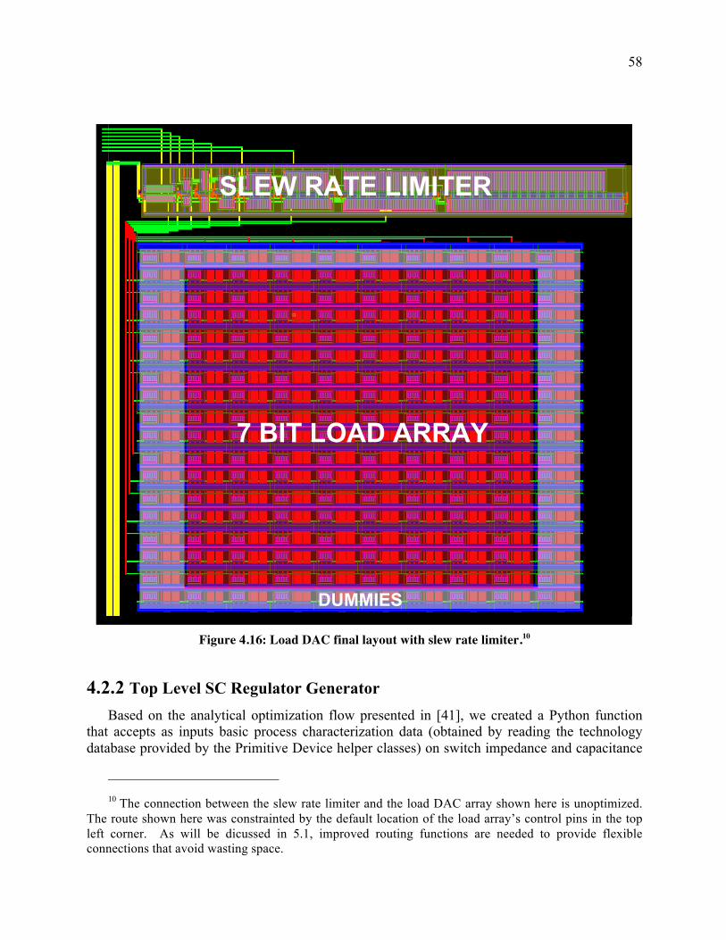
58
Figure 4.16: Load DAC final layout with slew rate limiter.10
Top Level SC Regulator Generator 4.2.2Based on the analytical optimization flow presented in [41], we created a Python function
that accepts as inputs basic process characterization data (obtained by reading the technology database provided by the Primitive Device helper classes) on switch impedance and capacitance
10 The connection between the slew rate limiter and the load DAC array shown here is unoptimized.
The route shown here was constrainted by the default location of the load array’s control pins in the top left corner. As will be dicussed in 5.1, improved routing functions are needed to provide flexible connections that avoid wasting space.
'800,(6
��%,7�/2$'�$55$<
6/(:�5$7(�/,0,7(5

59
density (see Figure 2.8) as well as target output power specifications. The function then determines the optimal switch and capacitor sizing for the regulator core and the optimal number of interleaved phases. Figure 4.17 shows a block diagram of a six phase SC regulator.
Figure 4.17: 6-phase instance of an interleaved switched-capacitor converter with per-phase lower bound control blocks.
The outputs of the system-level optimization are hierarchically passed to the generators for all of the sub-blocks. Figure 4.18 shows the hierarchical layouts of the three different converters targeting the specifications listed in Table 4.1. The top-level regulator generator inherits from the ArrayModule helper class (2.3.4.3) to instantiate the desired number of interleaved phases.
][jg]Y
9RXW9LQ
9LQ
9RXW 9LQ
9LQ
&�
&�
&�
&�
][jg]Y
9RXW9LQ
9LQ
9RXW 9LQ
9LQ
&�
&�
&�
&�
][jg]Y
9RXW9LQ
9LQ
9RXW 9LQ
9LQ
&�
&�
&�
&�
][jg]Y
9RXW9LQ
9LQ
9RXW 9LQ
9LQ
&�
&�
&�
&�
][jg]Y
9RXW9LQ
9LQ
9RXW 9LQ
9LQ
&�
&�
&�
&�
][jg]Y
9RXW9LQ
9LQ
9RXW 9LQ
9LQ
&�
&�
&�
&�

60
Figure 4.18: Final layouts of three complete SC regulator designs.
After the first iteration of the design flow has been completed, pre (see Figure 4.19 for the top-level schematic simulation of the 1 W regulator responding to load current steps) and post-layout simulations are run to evaluate the regulator performance, and the sizing flow is iterated to take the updated parasitic information into account. The automation of the design flow substantially lowers the cost of each iteration (in our implementation, each iteration is fully automated, and it takes around three hours to run), thus enabling a tighter tuning and verification of the regulator performance with respect to a manual flow.
Figure 4.19: Load transient step response simulation result.
�D� �E�
�F�
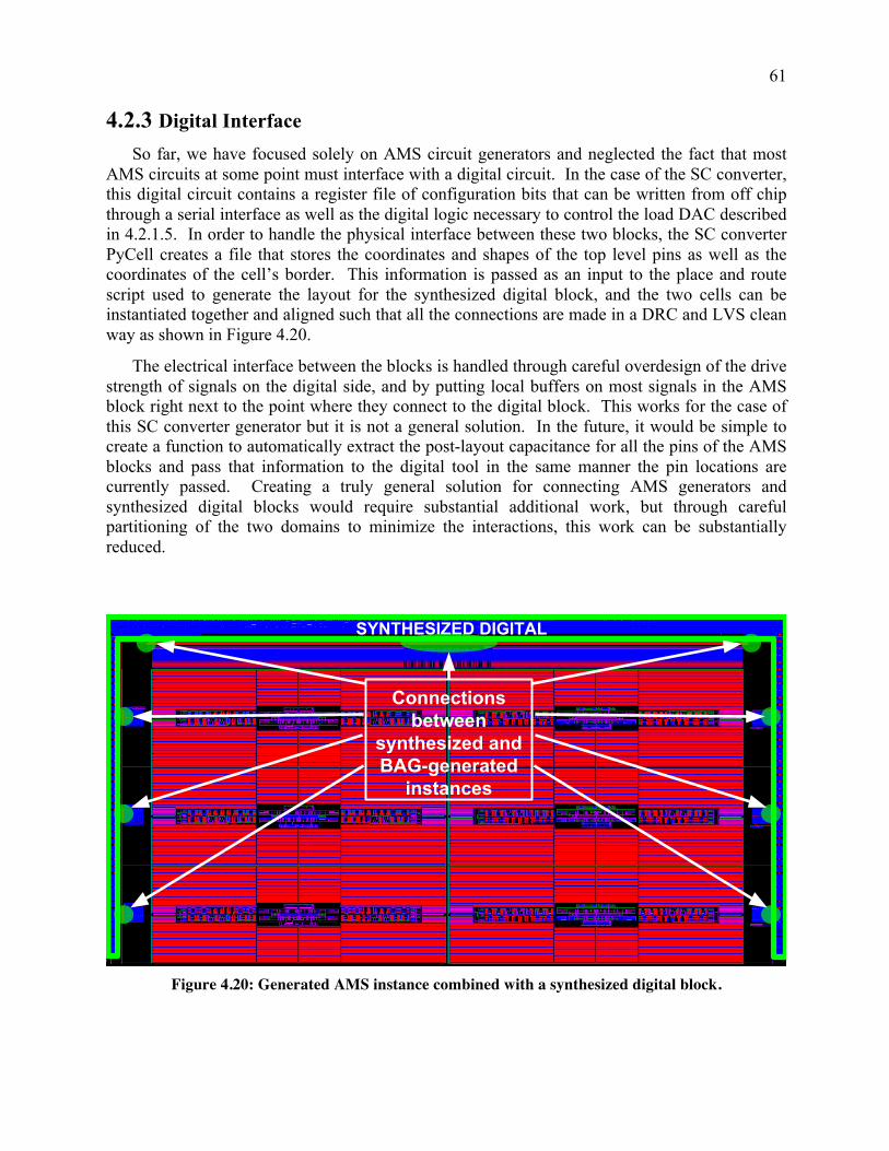
61
Digital Interface 4.2.3So far, we have focused solely on AMS circuit generators and neglected the fact that most
AMS circuits at some point must interface with a digital circuit. In the case of the SC converter, this digital circuit contains a register file of configuration bits that can be written from off chip through a serial interface as well as the digital logic necessary to control the load DAC described in 4.2.1.5. In order to handle the physical interface between these two blocks, the SC converter PyCell creates a file that stores the coordinates and shapes of the top level pins as well as the coordinates of the cell’s border. This information is passed as an input to the place and route script used to generate the layout for the synthesized digital block, and the two cells can be instantiated together and aligned such that all the connections are made in a DRC and LVS clean way as shown in Figure 4.20.
The electrical interface between the blocks is handled through careful overdesign of the drive strength of signals on the digital side, and by putting local buffers on most signals in the AMS block right next to the point where they connect to the digital block. This works for the case of this SC converter generator but it is not a general solution. In the future, it would be simple to create a function to automatically extract the post-layout capacitance for all the pins of the AMS blocks and pass that information to the digital tool in the same manner the pin locations are currently passed. Creating a truly general solution for connecting AMS generators and synthesized digital blocks would require substantial additional work, but through careful partitioning of the two domains to minimize the interactions, this work can be substantially reduced.
Figure 4.20: Generated AMS instance combined with a synthesized digital block.
6<17+(6,=('�',*,7$/
&RQQHFWLRQV�EHWZHHQ�
V\QWKHVL]HG�DQG�%$*�JHQHUDWHG�
LQVWDQFHV

62
Chapter 5 – Conclusion The number and complexity of analog/mixed-signal circuits included in modern SoC designs
is rising, and these circuits are increasingly becoming the primary critical bottleneck gating chip tapeouts even though they often occupy only a small portion of the total die area. In order to address this issue, we argued the need for a more automated methodology in AMS circuit design – specifically, that designers should no longer be focused on producing a sized schematic and layout of a singular circuit instance, but instead should produce circuit generators that can procedurally create schematics and layout of a circuit according to a set of input specifications utilizing the designer’s codified knowledge. Therefore, to ease the creation of these AMS circuit generators, we implemented a collection of Python-code called the Berkeley Analog Generator (BAG).
In order to reduce the learning curve for creating generators and to ease the adoption of the BAG framework, we borrowed heavily from the familiar manual design flow – especially for the initial steps of schematic and testbench-entry, which are nearly identical to the traditional flow. We chose Python as a user-friendly implementation language, and tried to structure the framework around an interactive flow that provides designers with an intermediate design exploration step after conceptualizing a new architecture, but before being tasked with writing code for a generator. While developing generators using the BAG framework, we noticed many design procedures relied on pre-characterizing certain key portions of the circuit. In this thesis, we demonstrated helper classes that assist with the creation and maintenance of simulation-based characterization information for device primitives as well as user-created cells. Other helper classes were created to enable circuits with variable structures and to assist with common sizing techniques like the method of logical effort.
We demonstrated the completeness of the BAG framework, i.e. that it can be used for a complete AMS design flow, with an integrated switched-capacitor regulator generator – a complex hierarchical system relevant to modern SoC architectures. By building hierarchical parameterized layouts, we were able to create a top level parameterized layout for the SC regulator and demonstrated its ability to handle different target aspect ratios and sizes. Initially we planned to use commercial AMS place-and-route tools driven by constraints for higher level layout generators because we assumed that it would be frustratingly difficult to create parameterized layouts for cells with many levels of hierarchy. However, as we added more functionality to the layout styles and built more complex manual PyCells for the SC converter, we found that we preferred the level of control that came from using PyCells as compared to a constraint-based automatic tool. It was very useful to be able to reuse the placement and routing methods in the Standard styles while still being able to add customized procedures for certain cells on top of the base style.
We also showed that, through judicious use of the PyCell correct-by-construction API and by constraining the layout to fit into one of the BAG layout styles, layout generators can be made portable from one process to another with few changes to the underlying code. This portability depends on the new process having a similar number of metal layers and generally similar design rules to the old process. If these requirements are met, even complex hierarchical blocks can be compiled for different processes using single PyCell source file.
63
5.1 Future Work The BAG framework is essentially functionally complete in that it can be used to create
generators for any kind of AMS circuit. Currently however, a generator writer implementing a design using the BAG framework might need to invest significant effort to e.g. use their preferred design or layout style because it is not yet enabled in the BAG framework. They might also encounter a problem related to a constraint imposed on the design stemming from the use of one of the helper functions or styles that are already in BAG. The potential improvements suggested in this section address one of these two problems by enabling more design techniques with the BAG framework or improving the speed and usability of those already in the framework.
In section 2.3.4.4, we described the BAG framework’s handling of veriloga blocks for use in testbench circuits, but it would be useful to have a more complete mixed-mode simulation capability available from within BAG. SPICE level simulation of complex analog circuits can be computationally expensive and have lengthy run times, so one common solution AMS designers employ is to simulate key blocks at the full SPICE level of accuracy while other blocks (e.g. control blocks) are simulated with faster methods using event-driven or behavioral models written in verilog or verilogams respectively. There are many tools for running mixed-mode simulations of this sort, and one can imagine a simple interface in BAG whereby each Module could have a default simulation method associated with it that could be adjusted as necessary.
Another simple improvement that could be easily implemented is a function for automatically calculating certain electrical parameters from post-layout parasitic extractions or post-layout simulations. For example, it would be useful to have a property associated with each pin of a Module that could return the effective capacitance seen looking into that pin which could be used for interfacing with digital synthesis tools or sizing chains of digital logic. The value could be calculated by recursively finding the capacitance of all connected pins and parsing the extracted netlist for parasitic wiring capacitances, or – depending on the accuracy desired – it could be calculated from simulation of the extracted netlist. All the necessary tools to implement this feature are already in BAG, but have not yet been assembled into a simple-to-use function.
The existing Standard styles are quite powerful in terms of enabling designers to create layouts with flexible aspect ratios that can implement most structures that appear in AMS circuits. However, there are several areas for improvement. Routing at the Standard Cell level is limited to only the lower two metal layers and the user must be careful to order the horizontal routing channels to avoid any shorts between vertical routes from the bottom of the cell to a higher horizontal routing channel as well as vertical routes from the top of the cell to a lower horizontal routing channel. Currently this limitation is avoided by creating extra horizontal routing channels for a single net, but the ideal solution is a more complex routing mechanism that can handle crossovers. Another limitation in Standard Cell is the inability to route from a device pin to a routing channel within a routing group that is not immediately adjacent to the device pin in the vertical stack. This precludes making layouts that look like the one in for the comparator in Figure 5.1 where there are PMOS precharge devices connected to nearly every internal node of the circuit that has five stacked device groups. This layout is very similar to a Standard Cell PyCell but is actually a fully custom PyCell because the designer wanted to avoid the current limitations of Standard Cell.

64
Figure 5.1 Manual PyCell of a comparator.
Another potential improvement for the Standard layout styles is to incorporate electromigration and thermal awareness into the PyCells. Currently, the geometric constraints for electromigration are calculated in custom code snippets within specific circuit generators (e.g. the power switches of the SC converter) once the initial sizing is determined. A more general method could be created where electrical information is passed to the layout by default. For example, the maximum current through every device could be stored in the Module and passed along with the netlist information to the PyCell. The Standard styles could then take this into account at each phase of the layout procedure and save the designer a lot of effort.
A final avenue for expanding the BAG framework is related to the restricted design rules that occur in more advanced technology nodes. In general, the complexity of code required to implement specific layout styles can be greatly simplified by drastically reducing the allowable design space through enforcing very strict routing grids and device placement grids. In older technologies, the performance penalty paid for oversimplifying the layout could be large, but in newer processes with multiple lithographic patterning steps for the lower layers, the DRC rules are already beginning to force extremely regular grid structures. Thus, the penalty for further restrictions might be small enough to be outweighed by the potential gains from the speedup in design iterations. If the grids are regular enough, layout could be performed on abstracted data structures expressed as a set of 2-dimensional arrays, i.e. one for each process layer. By characterizing the regular grid structure, post-layout parasitics could perhaps be estimated very quickly and with high accuracy. Writing placement and routing functions for such a simple representation of the layout would be much easier, and would hopefully lead to more experimentation on the part of designers. The speed of layout generators could potentially be dramatically increased, which could free designers to spend more time optimizing their designs at the system level.

65
Appendix A A.1 BAG Generator Code
This section has generator class listing files for example generators.
A.1.1 Load DAC Array
1. #!/usr/bin/python 2. # -‐*-‐ coding: utf-‐8 -‐*-‐ 3. from BAG.DesignDescription.ArrayModule import ArrayModule 4. from BAG.DesignDescription.GenericCell import GenericCell as GC 5. from numpy import floor, log2 6. 7. 8. class BAG_templates__load_dac_array(ArrayModule): 9. 10. """ 11. """ 12. 13. def inst_pin_formula(self, pin_name): 14. ''''' 15. Maps an instance pin name to a function that returns the net name. 16. 17. Args: 18. pin_name: (str) Instance pin name for a single instance of the 19. unit cell in the arry. 20. 21. Returns: 22. A function that takes two parameters (m,n) and returns a net_name. 23. The parameters identify the instance being operated on and the 24. net_name should be the net connected to the specified instance pin 25. <pin_name> on the instance indexed by (m,n). 26. 27. Example: 28. 29. Raises: 30. 31. BAG USER ACTION REQUIRED: Fill in the inst_pin_dict dictionary. 32. The keys to this dictionary are the names of the pins on 33. the unit cell (which should be the only cell in the template 34. schematic for the array module). The values for the keys 35. are functions. They can be other functions defined in this 36. class or lambda functions. Either way they must have two parameters 37. 'm' and 'n' which represent the outer and inner (or row and column) 38. iteration indexes that will be used in constructing the array. These 39. indexes are integers which can be used to form the net name that the 40. instance pin will be attached to. See some examples below: 41. 42. Examples: 43. 1 -‐ The corresponding pins on all instances are shorted to the same pins. 44. The 'a' and 'z' pins on all the unit cell instances are connected 45. to nets named 'in' and 'out'pins 46. inst_pin_dict = {'vdd': lambda m,n: 'vdd', 47. 'a': lambda m,n: 'in', 48. 'z': lambda m,n: 'out', 49. 'vss': lambda m,n: 'vss'} 50.

66
51. 2 -‐ The 'a' and 'z' pins on each unit cell instances are connected 52. to a net in a bus named 'in' and 'out' respectively 53. inst_pin_dict = {'vdd': lambda m,n: 'vdd', 54. 'a': lambda m,n: 'in<' + "%d"%(n) + '>', 55. 'z': lambda m,n: 'out<' + "%d"%(n) + '>', 56. 'vss': lambda m,n: 'vss'} 57. 58. 3 -‐ The 'a' and 'z' pins on each unit cell instances are connected 59. to a net in a bus named 'in' and 'out' respectively. The number 60. of cells connected to each net in the bus increases by 2 for each 61. additional net in the bus (one instance on net 'in<0>', two instances 62. on net 'in<1>', 4 instances on net 'in<2>' and so on. 63. inst_pin_dict = {'vdd': lambda m,n: 'vdd', 64. 'a': lambda m,n: 'in<' + "%d"%(floor(log2(n+1))) + '>', 65. 'z': lambda m,n: 'out<' + "%d"%(floor(log2(n+1))) + '>', 66. 'vss': lambda m,n: 'vss'} 67. ''' 68. 69. inst_pin_dict = {'control': lambda m, n: 'control', 70. 'VSS': lambda m, n: 'VSS', 'VDD': lambda m, n: \ 71. 'VDD'} 72. 73. return inst_pin_dict[pin_name] 74. 75. ## -‐-‐-‐-‐-‐-‐-‐-‐-‐-‐-‐-‐-‐-‐-‐-‐-‐-‐-‐ Example 1 for defining a tree structure -‐-‐-‐-‐-‐-‐-‐-‐-‐-‐-‐-‐ 76. ## This example assumes pin names 'in', 'out', 'vdd', and 'vss'. Modify as necessary.
77. ## Comment out the lines above defining inst_pin_dict and returning inst_pin_dict[pin_n
ame] 78. ## and uncomment this block of code as well as the other 2 blocks below labeled with 'E
xample 79. ## 1 for defining a tree structure' 80. # inst_pin_dict = {'vss': lambda m,n: 'vss', 81. # 'vdd': lambda m,n: 'vdd', 82. # 'a': self.instance_input_net, 83. # 'z': self.instance_output_net} 84. # 85. # return inst_pin_dict[pin_name] 86. # 87. # def instance_output_net(self,m,n) : 88. # Serves same purpose as 89. # if m == self.dim_0.value-‐1 : # last iteration 90. # return 'out' 91. # else : 92. # return 'int_' + "%d"%(int(m+1)) + '_' + "%d"%(int(n/self.radix.value)) 93. # 94. # 95. # def instance_input_net(self,m,n) : 96. # if m == 0 : # first iteration 97. # return 'in<' + "%d"%(int(n)) + '>' 98. # else : 99. # return 'int_' + "%d"%(int(m)) + '_' + "%d"%(int(n)) 100. ## -‐-‐-‐-‐-‐-‐-‐-‐-‐-‐-‐-‐-‐-‐-‐-‐-‐-‐-‐ Example 1 for defining a tree structure -‐-‐-‐-‐-‐-‐-‐-‐-‐-‐-‐-‐ 101. 102. def pin_formula(self, pin_name): 103. ''''' 104. Maps the cell pin names to functions that returns the net name. 105. 106. Args: 107. pin_name: (str) A cell pin name at the top level of the array cell. 108.
67
109. Returns: 110. A function that takes no parameters and returns a net_name. 111. 112. Example: 113. 114. Raises: 115. 116. BAG USER ACTION REQUIRED: Fill in the pin_dict dictionary. 117. The keys to this dictionary are the names of the pins on 118. the array cell (which should be the pin symbols in the template 119. schematic for the array module). The values for the keys 120. are functions. They can be other functions defined in this 121. class or lambda functions. These functions can access the parameters 122. of the array class including 'dim_0' and 'dim_1' which are the default a
rray 123. iteration indexes. The values returned by these functions 124. are the net names that should be connected to the pins. The pins will 125. be renamed so their names match the net names. 126. 127. Examples: 128. 1 -‐
The corresponding pins on all instances are shorted to the same pins. 129. The 'a' and 'z' pins on all the unit cell instances are connecte
d 130. to nets named 'in' and 'out'pins 131. pin_dict = {'vdd': lambda : 'vdd', 132. 'in': lambda : 'in', 133. 'out': lambda : 'out', 134. 'vss': lambda : 'vss'} 135. 136. 2 -‐ The 'a' and 'z' pins on each unit cell instances are connected 137. to a net in a bus named 'in' and 'out' respectively 138. pin_dict = {'vdd': lambda : 'vdd', 139. 'in': lambda : 'in<' + "%d"%(self.dim_1.value-‐
1) + ':0>', 140. 'out': lambda : 'out<' + "%d"%(self.dim_1.value-‐
1) + ':0>', 141. 'vss': lambda : 'vss'} 142. ''' 143. 144. ## -‐-‐-‐-‐-‐-‐-‐-‐-‐-‐-‐-‐-‐-‐-‐-‐-‐-‐-‐ Example 1 for defining a tree structure -‐-‐-‐-‐-‐-‐-‐-‐-‐-‐-‐-‐ 145. ## This example assumes pin names 'in', 'out', 'vdd', and 'vss'. Modify as nece
ssary. 146. ## Comment out the lines below defining pin_dict and uncomment this code block
147. ## as well as the other 2 blocks above/below labeled with 'Example 1 for definin
g a tree structure' 148. # pin_dict = {'vss': lambda : 'vss', 149. # 'in': lambda : 'in<' + "%d"%(int(2**self.dim_0.value-‐
1)) + ':0>', 150. # 'out': lambda : 'out', 151. # 'vdd': lambda : 'vdd', 152. # 'vss': lambda : 'vss'} 153. ## -‐-‐-‐-‐-‐-‐-‐-‐-‐-‐-‐-‐-‐-‐-‐-‐-‐-‐-‐ Example 1 for defining a tree structure -‐-‐-‐-‐-‐-‐-‐-‐-‐-‐-‐-‐ 154. 155. pin_dict = {'control': lambda : 'control', 'VSS': lambda : \ 156. 'VSS', 'VDD': lambda : 'VDD'} 157. return pin_dict[pin_name] 158. 159. def testbench_formula(self): 160. '''''

68
161. How to alter the testbench instances and their inst_pins so they 162. can connect properly to the new 163. testbench_pin_dict = { 'DNL' : { 'vdd': lambda 'vdd' 164. ' } 165. ''' 166. 167. pass 168. 169. # testbench_pin_dict = 170. 171. def instance_formula(self, m, n): 172. ''''' 173. BAG USER ACTION SUGGESTED: Formula generates the suffix 174. for the iterated unit cells. 175. ''' 176. 177. return '%04d' % int(m) + '_' + '%04d' % int(n) 178. 179. def __init__( 180. self, 181. prj, 182. parent=None, 183. in_testbench=False, 184. ): 185. generic_cell = GC('load_dac_array', 'BAG_templates') 186. ArrayModule.__init__(self, prj, generic_cell, parent, 187. in_testbench) 188. 189. # self.dim_0 must be an integer but self.dim_1 can be either an integer
or a function that 190. # returns an integer. 191. 192. self.dim_0 = 1 193. self.dim_1 = 1 194. 195. 196. # # -‐-‐-‐-‐-‐-‐-‐-‐-‐-‐-‐-‐-‐-‐-‐-‐-‐-‐-‐ Example 1 for defining a tree structure -‐-‐-‐-‐-‐-‐
-‐-‐-‐-‐-‐-‐ 197. # # This example assumes pin names 'in', 'out', 'vdd', and 'vss'. Modif
y as necessary. 198. # # Comment out the 2 lines above defining self.dim_0 and self.dim_1 and
uncomment this code block 199. # # as well as the other 2 blocks above labeled with 'Example 1 for defi
ning a tree structure' 200. # self.radix = self.add_design_parameter(DP(yaml_param_dict='radix',modu
le_handle=self,callback=self.update_array)) 201. # self.radix = 4 202. # self.num_bits = self.add_design_parameter(DP(yaml_param_dict='num_bits
',module_handle=self,callback=self.update_array)) 203. # self.num_bits = 4 204. # self.dim_0.set_expression('int(numpy.ceil(self.module.num_bits.value/n
umpy.log2(self.module.radix.value)))') 205. # self.dim_1 = lambda outer_iter: int((2**self.num_bits.value)/(self.rad
ix.value**outer_iter)) 206. # # -‐-‐-‐-‐-‐-‐-‐-‐-‐-‐-‐-‐-‐-‐-‐-‐-‐-‐-‐ Example 1 for defining a tree structure -‐-‐-‐-‐-‐-‐
-‐-‐-‐-‐-‐-‐ 207. 208. # # -‐-‐-‐-‐-‐-‐-‐-‐-‐-‐-‐-‐-‐-‐-‐-‐-‐-‐-‐ Example 2 for defining a tree structure -‐-‐-‐-‐-‐-‐-‐
-‐-‐-‐-‐-‐ 209. # self.dim_1 = lambda outer_iter: (2^outer_iter.value) #Use this definit
ion for self.dim_1 if the second dimension

69
210. # #of the array depends on the level as in a decoder or other
211. # #tree-‐like circuit. The function you write should take a single
212. # #parameter representing the outer iteration variable
213. # outer_iter = 0 # inner_iter = 2^0 = 1
214. # / \ 215. # outer_iter = 1 # # inner_iter = 2^1 =
2 216. # / \ / \ 217. # outer_iter = 2 # # # # inner_iter = 2^2 =
4 218. # # -‐-‐-‐-‐-‐-‐-‐-‐-‐-‐-‐-‐-‐-‐-‐-‐-‐-‐-‐ Example 2 for defining a tree structure -‐-‐-‐-‐-‐-‐-‐
-‐-‐-‐-‐-‐
A.1.2 DCDC Phase Unit Cell Generator
1. #!/usr/bin/python 2. # -‐*-‐ coding: utf-‐8 -‐*-‐ 3. 4. ##-‐-‐-‐-‐-‐-‐-‐-‐-‐-‐-‐-‐-‐-‐-‐-‐-‐-‐-‐-‐-‐-‐-‐-‐-‐-‐-‐-‐-‐-‐-‐-‐-‐-‐-‐-‐-‐-‐-‐-‐-‐-‐-‐-‐-‐-‐-‐-‐-‐-‐-‐-‐-‐-‐-‐-‐-‐-‐-‐-‐ 5. ## import modules 6. ##-‐-‐-‐-‐-‐-‐-‐-‐-‐-‐-‐-‐-‐-‐-‐-‐-‐-‐-‐-‐-‐-‐-‐-‐-‐-‐-‐-‐-‐-‐-‐-‐-‐-‐-‐-‐-‐-‐-‐-‐-‐-‐-‐-‐-‐-‐-‐-‐-‐-‐-‐-‐-‐-‐-‐-‐-‐-‐-‐-‐ 7. 8. """ 9. MODULE BAG_templates__conv_unit_cell2_wocap 10. 11. Fill in the funciton of this design module here 12. 13. 14. """ 15. 16. from BAG.DesignDescription.VarStructDesignModule import VarStructDesignModule 17. from BAG.DesignDescription.GenericCell import GenericCell as GC 18. from pylab import ceil 19. from copy import copy, deepcopy 20. import pdb 21. from BAG.DesignDescription.logical_effort import logical_effort 22. import yaml 23. 24. 25. ##-‐-‐-‐-‐-‐-‐-‐-‐-‐-‐-‐-‐-‐-‐-‐-‐-‐-‐-‐-‐-‐-‐-‐-‐-‐-‐-‐-‐-‐-‐-‐-‐-‐-‐-‐-‐-‐-‐-‐-‐-‐-‐-‐-‐-‐-‐-‐-‐-‐-‐-‐-‐-‐-‐-‐-‐-‐-‐-‐-‐ 26. ## class DesignModule 27. ##-‐-‐-‐-‐-‐-‐-‐-‐-‐-‐-‐-‐-‐-‐-‐-‐-‐-‐-‐-‐-‐-‐-‐-‐-‐-‐-‐-‐-‐-‐-‐-‐-‐-‐-‐-‐-‐-‐-‐-‐-‐-‐-‐-‐-‐-‐-‐-‐-‐-‐-‐-‐-‐-‐-‐-‐-‐-‐-‐-‐ 28. 29. class BAG_templates__conv_unit_cell2_wocap(VarStructDesignModule, 30. logical_effort): 31. 32. """ 33. """ 34. 35. def __init__( 36. self, 37. prj, 38. parent=None, 39. in_testbench=False, 40. ): 41. '''''

70
42. If project_name is empty then a new user_project will be created 43. ....(in both the CAD and python directories) 44. ''' 45. 46. generic_cell = GC('conv_unit_cell2_wocap', 'BAG_templates') 47. VarStructDesignModule.__init__(self, prj, generic_cell, parent, 48. in_testbench) 49. 50. # self.force_schematic = True 51. 52. logical_effort.__init__(self) 53. self.width_finger_pairs = [['M5_finger_w', 'M5_fingers']] 54. self.rBulk = 1.0 55. self.areaUnitCap = 1.0 56. self.interleaving = 1 57. self.HoverW = 0.0 58. self.route4LVS = 'False' 59. self.widthM5 = 0.0 60. self.cachedParameterFile = '' 61. self.path2CompCore = '' 62. self.powerLevel = '' 63. self.default_pycell_lib_cell = \ 64. 'demo_cells_oa_lib/DCDC2OutOfPhaseWoCaps' 65. 66. def simple_size(self): 67. pass 68. 69. def set_default_sizes( 70. self, 71. g_mult=1, 72. g_width=None, 73. g_length=None, 74. g_pnrat=None, 75. vin=2.0, 76. vref=0.9, 77. unit_inv_cap=1e-‐15, 78. switch_load_cap=2.0e-‐12, 79. target_fanout=4.0, 80. nonoverlap_ratio=2.0, 81. ): 82. 83. ccell = self 84. prj = self.prj 85. 86. # size the switches 87. 88. gate_cap_ff_per_um = 1.0 # extract this number 89. total_switch_width = switch_load_cap / 1e-‐15 \ 90. / gate_cap_ff_per_um * 1e-‐6 91. for the_cell in [ccell.I19.I0, ccell.I20.I0]: 92. for the_cap in [the_cell.C1, the_cell.C2]: 93. the_cap.set_parameters('W', 500e-‐6) 94. the_cap.cap_mult = 10 95. the_cap.mult = 280 96. the_cell.p_switch_width = g_width * 10 97. the_cell.n_switch_width = g_width * 10 98. the_cell.n_switch_mult = int(total_switch_width 99. / the_cell.n_switch_width.value) 100. the_cell.p_switch_mult = int(total_switch_width 101. / the_cell.p_switch_width.value) 102. the_cell.cfly = 2.8e-‐10

71
103. the_cell.cfly_ic = vref 104. 105. unit_inverter_gate_cap = g_width * 3 * gate_cap_ff_per_um / 1e-‐6 106. switch_gate_cap = ccell.I20.I0.n_switch_width.value \ 107. * the_cell.n_switch_mult.value * gate_cap_ff_per_um / 1e-‐6 108. switch_load = int(switch_gate_cap / unit_inverter_gate_cap) 109. if not g_width: 110. dummy_M = prj.classes['BAG_prim__nmos4'](prj) 111. dummy_M.W = 0.0 112. g_width = 2.0 * dummy_M.W.value 113. del dummy_M 114. if not g_length: 115. dummy_M = prj.classes['BAG_prim__nmos4'](prj) 116. dummy_M.L = 0.0 117. g_length = dummy_M.L.value 118. del dummy_M 119. if not g_pnrat: 120. g_pnrat = 1.6 121. ccell.set_parameters('PN_ratio', g_pnrat) 122. ccell.set_parameters('L', g_length) 123. ccell.set_parameters('W', g_width) 124. ccell.set_parameters('stack', 1) 125. 126. # set capacitor cell driver sizes 127. 128. ccell.I20.pnrat = g_pnrat * 2 # multiply by 2 because this is a nor gat
e 129. ccell.I20.pgatedrive_W = g_width 130. ccell.I19.pnrat = g_pnrat * 2 # multiply by 2 because this is a nor gat
e 131. ccell.I19.pgatedrive_W = g_width 132. gatedrive_mult = ceil(switch_load / (target_fanout * 3 / 5.0)) # logica
l effor of nor is 3/5 133. ccell.I20.pgatedrive_mult = gatedrive_mult 134. ccell.I19.pgatedrive_mult = gatedrive_mult 135. 136. ccell.sw_cap = switch_load_cap 137. ccell.critical_path.set_default_sizes(g_mult, g_width, 138. g_length, g_pnrat) 139. ccell.critical_path.adjust_mults(gatedrive_mult, 140. target_fanout=target_fanout, 141. nonoverlap_ratio=nonoverlap_ratio) 142. 143. # these phase_splitters drive clock of the toggle flop 144. 145. load_mult = ceil(ccell.critical_path.dflop.pg_mult.value 146. + ccell.critical_path.dflop.tristate_mult_2.value 147. + ccell.critical_path.dflop.tristate_mult.value) 148. ccell.phase_split_long.size_to_drive(load_mult, target_fanout) 149. 150. # comparator should actually sized based on delay and mistmatch constrai
nts 151. 152. mult_normalization_factor = \ 153. ccell.phase_split_long.inverting_stage.W.value \ 154. / ccell.phase_split_long.buf_stage_1.W.value 155. ps_mult = ccell.phase_split_long.buf_stage_1.mult.value \ 156. + mult_normalization_factor \ 157. * ccell.phase_split_long.inverting_stage.mult.value 158. comp_mult = ceil(ps_mult / target_fanout) 159. ccell.comparator.set_default_sizes(comp_mult, g_width)

72
160. 161. # size gates in clk_output driver 162. # should be sized based on comparator 163. 164. clk_driver_mult = 4 165. ccell.pull_up_keeper.mult = clk_driver_mult * 2 166. ccell.pull_down_keeper.mult = clk_driver_mult 167. ccell.pull_down_reset.mult = clk_driver_mult 168. ccell.pull_up_long_1.set_default_sizes(g_mult=g_mult, 169. g_width=g_width, g_length=g_length, g_pnrat=g_pnrat) 170. ccell.pull_up_long_2.set_default_sizes(g_mult=g_mult, 171. g_width=g_width, g_length=g_length, g_pnrat=g_pnrat) 172. ccell.pull_up_long_1.pull_up_mult = clk_driver_mult * 2 173. ccell.pull_up_long_2.pull_up_mult = clk_driver_mult * 2 174. 175. # make sure reset parameter uses thick gate devices so it can handle ful
l 176. # scale voltages on its inputs 177. 178. ccell.reset_inv_fs.set_parameters('device_intent', 179. 'high_voltage') 180. dummy_M = prj.classes['BAG_prim__nmos4'](prj) 181. dummy_M.device_intent = 'high_voltage' 182. dummy_M.W = 0.0 183. dummy_M.L = 0.0 184. the_width = dummy_M.W.value 185. the_length = dummy_M.L.value 186. del dummy_M 187. ccell.reset_inv_fs.W = the_width 188. ccell.reset_inv_fs.L = the_length 189. 190. # pnration should be fine 191. 192. def get_pycell_to_bag_mapping(self, lib_cell): 193. if lib_cell == 'demo_cells_oa_lib/DCDC2OutOfPhaseWoCaps': 194. pycell_to_bag_mapping = [['control', self.control_core, 195. 'BAG_std_cells_oa/comp_core2'], ['load', 196. self.load_dac, 'BAG_std_cells_oa/load_dac'], ['slew' 197. , self.load_dac.slew_rate_limiter, 198. 'BAG_std_cells_oa/slew_rate_limiter'], ['switches', 199. self.swcap_w_driver_out_phase, 200. 'demo_cells_oa_lib/DCDC_unit_cell_noM5']] 201. 202. # ['caps',, 'demo_cells_oa_lib/dense_unit_
capNM'] 203. 204. return pycell_to_bag_mapping 205. 206. def pycell_mapper(self, lib_cell, use_pycell_defaults=False): 207. ''''' 208. This function should map the BAG parameters to pycell parameters and ret
urn a dictionary 209. which can then be passed (through a yaml file) to the pycell 210. ''' 211. 212. the_params = {} 213. the_cell = GC(self.cell_name, self.inst_lib_name) 214. 215. # the pycell_to_bag_mapping should help map the subpycells to BAG module
s

73
216. # each row should be of the format [ pycell_instance_name, bag_module, lib_cell]
217. 218. if lib_cell == 'demo_cells_oa_lib/DCDC2OutOfPhaseWoCaps': 219. self._dict_for_param_file = {} 220. self._dict_for_param_file['instance_parameters'] = dict() 221. for (pycell_instance_name, bag_module, lib_cell) in \ 222. self.get_pycell_to_bag_mapping(lib_cell): 223. 224. self._dict_for_param_file['instance_parameters' 225. ][pycell_instance_name] = \ 226. bag_module.pycell_mapper(lib_cell) 227. self._dict_for_param_file.update(dict( 228. rBulk=self.rBulk, 229. areaUnitCap=self.areaUnitCap, 230. interleaving=self.interleaving, 231. HoverW=self.HoverW, 232. route4LVS=self.route4LVS, 233. widthM5=self.widthM5, 234. cachedParameterFile=self.cachedParameterFile, 235. loadBits=self.load_dac.bits.value, 236. vRefWidth=self.parent_module.parent_module.parent_module.vRefWid
th, 237. )) 238. self.param_file = self.prj.project_directory + '/OOP_' \ 239. + self.powerLevel + '.yaml' 240. yaml_string = yaml.dump(self._dict_for_param_file) 241. print 'DCDC2OutOfPhaseWoCaps yaml parameter file %s' \ 242. % self.param_file 243. the_file = open(self.param_file, 'w') 244. the_file.write(yaml_string) 245. the_file.close() 246. the_params = {'param_file': self.param_file} 247. 248. # 'polyDensity': float(self.polyDensity.value), 249. 250. the_params.update(self._dict_for_param_file) 251. if not use_pycell_defaults: 252. return the_params 253. else: 254. return {} 255. 256. def pycell_reverse_mapper(self, result_props): 257. ''''' 258. This level doesn't get the control core and switch cell parameters in th
e result_props 259. 260. ''' 261. 262. self.M5_finger_w = result_props['M5_finger_w'] 263. self.M5_fingers = result_props['M5_fingers'] 264. 265. # ['switches', self.swcap_w_driver_out_phase, "demo_cells_oa_lib/DCDC_un
it_cell_noM5"], 266. # pycell_reverse_mapper for swcap_w_driver_out_phase gets called automat
icallys 267. 268. # swcap.I0.M1M4_finger_w = result_props['M1M4_finger_w']*1e-‐6 269. # swcap.I0.M1M4_fingers = result_props['M1M4_fingers'] 270. # swcap.I0.M2M3_finger_w = result_props['M2M3_finger_w']*1e-‐6 271. # swcap.I0.M2M3_fingers = result_props['M2M3_fingers']

74
272. # swcap.I0.M6M9_finger_w = result_props['M6M9_finger_w']*1e-‐6 273. # swcap.I0.M6M9_fingers = result_props['M6M9_fingers'] 274. # swcap.I0.M7M8_finger_w = result_props['M7M8_finger_w']*1e-‐6 275. # swcap.I0.M7M8_fingers = result_props['M7M8_fingers'] 276. 277. # swcap.I0.M1M4_true_mult = result_props['M1M4_true_mult'] 278. # swcap.I0.M2M3_true_mult = result_props['M2M3_true_mult'] 279. # swcap.I0.M6M9_true_mult = result_props['M6M9_true_mult'] 280. # swcap.I0.M7M8_true_mult = result_props['M7M8_true_mult'] 281. 282. def create_layout_for_lvs( 283. self, 284. flatten=False, 285. use_pycell_defaults=False, 286. route4LVS=False, 287. ): 288. 289. the_cell = GC(self.cell_name, self.inst_lib_name) 290. pcell = GC('DCDC2OutOfPhaseWoCaps', 'demo_cells_oa_lib') 291. lib_cell = pcell.lib_name + '/' + pcell.cell_name 292. if route4LVS: 293. self.route4LVS = 'True' 294. else: 295. self.route4LVS = 'False' 296. param_dict = self.pycell_mapper(lib_cell, use_pycell_defaults) 297. 298. # layout : schematic 299. 300. pin_dict = {'pmos_bias': 'pmos_slew_bias', 301. 'nmos_bias': 'nmos_slew_bias'} 302. 303. # incomplete 304. # pin_dict = zip(self.pins.keys(),self.pins.keys()) 305. # pdb.set_trace() 306. 307. result_props = \ 308. self.prj.db.instantiate_layout_for_extraction(the_cell, 309. pcell, param_dict, pin_dict, flatten=flatten) 310. self.result_props = result_props 311. 312. def _perform_structure_update(self): 313. ''''' 314. The user should implement this function so the structure of the 315. module is updated based on the parameter 316. values. It will be called triggered when any structural design 317. parameters are altered although it will not actually be run until 318. update_structure is called. 319. ''' 320. 321. VarStructDesignModule._perform_structure_update(self) 322. self.pins['load_code'].pin_name = 'load_code<%d:0>' \ 323. % (self.load_dac.bits.value -‐ 1) 324. self.pins['load_code'].net_name = 'load_code<%d:0>' \ 325. % (self.load_dac.bits.value -‐ 1) 326. self._update_connections_from_children() 327. for x in self.connections: 328. if x.net_name == 'load_code': 329. x.net_name = 'load_code<%d:0>' \ 330. % (self.load_dac.bits.value -‐ 1) 331. if x.pin_name == 'load_code' and not x.inst_name: 332. x.pin_name = 'load_code<%d:0>' \

75
333. % (self.load_dac.bits.value -‐ 1) 334. 335. # self.pin_order = [self.pins[x].pin_name for x in self._orig_pin_order
] 336. 337. def _update_connections_from_children(self): 338. ''''' 339. Refresh the connections on this module by starting with the original sch
ematic connections 340. (from the yaml file) and then update them according to the current pins
object 341. in all child instances 342. ''' 343. 344. self.connections = deepcopy(self._original_connections) 345. for (inst_name, inst) in self.instances.iteritems(): 346. for (orig_pin_name, pin) in inst.pins.iteritems(): 347. if not pin.pin_name == orig_pin_name: 348. 349. # print inst_name,pin['pin_name'],orig_pin_name 350. # indicates this pin name has been changed due to a structur
al change 351. # so we should update that in the current parent module 352. 353. for x in self.connections: 354. if x.inst_name == inst_name and x.pin_name \ 355. == orig_pin_name: 356. x.pin_name = pin.pin_name 357. x.orig_pin_name = orig_pin_name 358. break # should only be one pin with that name 359. 360. def generate_layout(self): 361. '''''Generates the layout of the current Module. Abstract function 362. that should be implemented by all functions that inherit from 363. DesignModule. 364. ....''' 365. 366. pass 367. 368. def design( 369. self, 370. DCDC_params={}, 371. the_switch_params={}, 372. num_phases=10, 373. L=60e-‐9, 374. target_effort=None, 375. cell_height=None, 376. switch_device_intent='standard', 377. later_stage_device_intent='fast', 378. power_scale_factor=0.6, 379. **kwargs 380. ): 381. '''''Abstract function that should be implemented by all functions 382. ....that inherit from DesignModule. 383. ....''' 384. 385. oop = self 386. 387. # power_scale_factor = 0.25 388.

76
389. self.update_device_char() # There aren't any nmos or pmos at this level so it probably uses defaults
390. for arg in ( 391. 'pnrat', 392. 'stack_2n', 393. 'cgate', 394. 'cgaten', 395. 'cgatep', 396. 'stack_3n', 397. 'stack_2p', 398. 'stack_3p', 399. 'gamma', 400. 'tinv', 401. ): 402. exec "%s = kwargs.get('%s',self.%s)" % (arg, arg, arg) # put argume
nt into local variables for this function 403. oop.set_parameters('pcell_id', 'basic') 404. if self.prj.__dict__.has_key('Wmin'): 405. Wmin = self.prj.Wmin 406. else: 407. Wmin = 400e-‐9 408. snap = self.prj.snap 409. 410. oop.control_core.simple_size() 411. 412. if cell_height: 413. oop.control_core.cell_height = cell_height 414. 415. # set M5 size 416. 417. self.M5_fingers = 1 418. self.M5_finger_w = DCDC_params['instance_parameters']['OOP' 419. ]['M5width'] / 1e6 420. self.rBulk = DCDC_params['instance_parameters']['OOP']['rBulk'] 421. self.areaUnitCap = DCDC_params['instance_parameters']['OOP' 422. ]['areaUnitCap'] 423. self.interleaving = DCDC_params['instance_parameters']['OOP' 424. ]['interleaving'] 425. self.HoverW = DCDC_params['instance_parameters']['OOP']['HoverW' 426. ] 427. self.widthM5 = DCDC_params['instance_parameters']['OOP' 428. ]['M5width'] 429. self.cachedParameterFile = './OOPParams_' \ 430. + DCDC_params['powerLevel'] + '.yaml' 431. self.path2CompCore = 'control_core_' + DCDC_params['powerLevel'] 432. self.powerLevel = DCDC_params['powerLevel'] 433. self.fix_widths() 434. M5_load_cap = self.M5_in_phase.total_width * cgate 435. 436. oop.swcap_w_drivers_in_phase.simple_size(the_switch_params=the_switch_pa
rams, 437. switch_device_intent=switch_device_intent, 438. M5_load_cap=M5_load_cap) 439. oop.swcap_w_driver_out_phase.simple_size(the_switch_params=the_switch_pa
rams, 440. switch_device_intent=switch_device_intent, 441. M5_load_cap=M5_load_cap) 442. 443. # oop.Cfly_in_phase.simple_size() 444. # oop.cfly_out_phase.simple_size() 445.

77
446. cur_volt_pair = [(1.0, 0.8), (1.0, 1.2)] 447. oop.load_dac.design(bits=7, cur_volt_pairs=cur_volt_pair, 448. num_phases=num_phases) 449. 450. # figure out which path has the highest fanout 451. 452. partitions = the_switch_params['swPartitions'] 453. nov_ratio = 1.0 454. nov_pg_ratio = 1 / 4.0 # pg inputs to are 4 times smaller than what the
y are driving 455. 456. nov_driver = oop.control_core.critical_path.nov_ls.nov_high 457. 458. # intrinsic delay factors 459. 460. p_nor2 = (pnrat * stack_2p + 2) / (1 + pnrat) 461. p_nand2 = (pnrat * 2 + stack_2n) / (1 + pnrat) 462. p_flying_inv = (stack_3p * pnrat + 1) / (1 + pnrat) 463. p_nov_h = (2 * pnrat + 1) / (1 + pnrat) 464. p_nov_l = (pnrat + 2) / (1 + pnrat) 465. p_pg = 1 466. 467. delay_fanout = 4.0 468. 469. # side loads from layout parasitics 470. 471. cin_8_side_load = 5e-‐15 472. 473. C1 = power_scale_factor * partitions \ 474. * (oop.swcap_w_drivers_in_phase.I0.I0.M1.W.value 475. * oop.swcap_w_drivers_in_phase.I0.I0.M1.mult.value 476. * cgatep) 477. C2 = power_scale_factor * partitions \ 478. * (oop.swcap_w_drivers_in_phase.I0.I0.M2.W.value 479. * oop.swcap_w_drivers_in_phase.I0.I0.M2.mult.value 480. * cgaten) 481. C3 = power_scale_factor * partitions \ 482. * (oop.swcap_w_drivers_in_phase.I0.I0.M3.W.value 483. * oop.swcap_w_drivers_in_phase.I0.I0.M3.mult.value 484. * cgaten) 485. C4 = power_scale_factor * partitions \ 486. * (oop.swcap_w_drivers_in_phase.I0.I0.M4.W.value 487. * oop.swcap_w_drivers_in_phase.I0.I0.M4.mult.value 488. * cgatep) 489. C5 = power_scale_factor * oop.M5_out_phase.W.value \ 490. * oop.M5_out_phase.mult.value * cgaten 491. C6 = power_scale_factor * partitions \ 492. * (oop.swcap_w_drivers_in_phase.I0.I0.M6.W.value 493. * oop.swcap_w_drivers_in_phase.I0.I0.M6.mult.value 494. * cgatep) 495. C7 = power_scale_factor * partitions \ 496. * (oop.swcap_w_drivers_in_phase.I0.I0.M7.W.value 497. * oop.swcap_w_drivers_in_phase.I0.I0.M7.mult.value 498. * cgaten) 499. C8 = power_scale_factor * partitions \ 500. * (oop.swcap_w_drivers_in_phase.I0.I0.M8.W.value 501. * oop.swcap_w_drivers_in_phase.I0.I0.M8.mult.value 502. * cgaten) 503. C9 = power_scale_factor * partitions \ 504. * (oop.swcap_w_drivers_in_phase.I0.I0.M9.W.value 505. * oop.swcap_w_drivers_in_phase.I0.I0.M9.mult.value
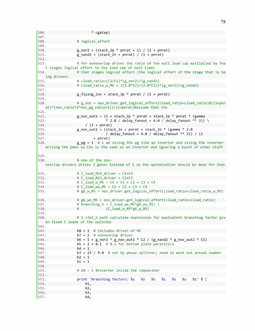
78
506. * cgatep) 507. 508. # logical_effort 509. 510. g_nor2 = (stack_2p * pnrat + 1) / (1 + pnrat) 511. g_nand2 = (stack_2n + pnrat) / (1 + pnrat) 512. 513. # for nonoverlap driver the ratio of the out1 load cap mutliplied by tha
t stages logical effort to the load cap of out2 times 514. # that stages logical effort (the logical effort of the stage that is be
ing driven) 515. # cload_ratio=(C2/C1)*(g_nor2)/(g_nand2) 516. # cload_ratio_w_M5 = ((3.0*C2)/(2.0*C1))*(g_nor2)/(g_nand2) 517. 518. g_flying_inv = stack_3p * pnrat / (1 + pnrat) 519. 520. # g_nov = nov_driver.get_logical_effort(cload_ratio=cload_ratio)#((1+pnr
at)*(nov_ratio*2*nov_pg_ratio+1))/(1+pnrat)#assume that the 521. 522. g_nov_out2 = (1 + stack_2p * pnrat + stack_2p * pnrat * (gamma 523. * 2.0 / delay_fanout + 4.0 / delay_fanout ** 3)) \ 524. / (1 + pnrat) 525. g_nov_out1 = (stack_2n + pnrat + stack_2n * (gamma * 2.0 526. / delay_fanout + 4.0 / delay_fanout ** 3)) / (1 527. + pnrat) 528. g_pg = 1 # i am sizing the pg like an inverter and sizing the inverter
driving the pmos so Cin is the same as an inverter and ignoring a bunch of other stuff
529. 530. # one of the non-‐
overlap drivers drives 3 gates instead of 2 so the opitmization should be done for that
531. # C_load_M14_driver = C1+C4 532. # C_load_M23_driver = C2+C3 533. # C_load_w_M5 = C5 + C1 + C2 + C3 + C4 534. # C_load_wo_M5 = C1 + C2 + C3 + C4 535. # g6_w_M5 = nov_driver.get_logical_effort(cload_ratio=cload_ratio_w_M5)
536. # g6_wo_M5 = nov_driver.get_logical_effort(cload_ratio=cload_ratio) 537. # branching_5 = C_load_wo_M5*g6_wo_M5/ \ 538. # (C_load_w_M5*g6_w_M5) 539. 540. # 1 clk2_h path calculate expression for equivalent branching factor giv
en fixed C loads of the switches 541. 542. b8 = 1 # includes driver of M5 543. b7 = 2 # nonoverlap driver 544. b6 = 1 + g_nor2 * g_nov_out1 * C2 / (g_nand2 * g_nov_out2 * C1) 545. b5 = 2 + 0.1 # 0.1 for bottom plate parasitics 546. b4 = 1 547. b3 = 25 / 9.0 # set by phase splitter; need to work out actual number 548. b2 = 1 549. b1 = 1 550. 551. # b0 = 1 #inverter inside the comparator 552. 553. print 'Branching factors: %s %s %s %s %s %s %s' % ( 554. b1, 555. b2, 556. b3, 557. b4,

79
558. b5, 559. b6, 560. b7, 561. ) 562. 563. # 2 calculate optimal fanout per stage 564. 565. g1 = 1 # inverter inside comparator (second stage with fixed size) 566. g2 = g_pg # pass gate in d flop 567. g3 = 1 # 568. g4 = 1 # stage 1 of phase splitter 569. g5 = 1 # stage 2 of phase splitter 570. g6 = 1 # level shift inverter 571. g7 = g_nov_out2 572. g8 = g_nand2 573. 574. cin1 = oop.control_core.comparator.Wn.value \ 575. * oop.control_core.comparator.nmult_inv2.value * cgaten \ 576. + oop.control_core.comparator.Wp.value \ 577. * oop.control_core.comparator.pmult_inv2.value * cgatep 578. 579. # cin1 = 0.4e-‐
6*(cgaten+pnrat*cgatep) #(minimum sized inverter (with M1 min area constraint)) 580. 581. G = g1 * g2 * g3 * g4 * g5 * g6 * g7 * g8 582. F = C1 / cin1 583. B = b1 * b2 * b3 * b4 * b5 * b6 * b7 * b8 584. PE = G * F * B 585. h = PE ** (1 / 8.0) 586. 587. if target_effort: 588. h = target_effort 589. self.target_effort = h 590. 591. # now use this to size the path 592. # size the M1 and M6 nand gates 593. # pdb.set_trace() 594. 595. for driver in (oop.swcap_w_drivers_in_phase.M1_driver, 596. oop.swcap_w_drivers_in_phase.M6_driver, 597. oop.swcap_w_driver_out_phase.M1_driver, 598. oop.swcap_w_driver_out_phase.M6_driver): 599. cin8_nand = driver.size_for_effort( 600. pnrat=pnrat, 601. stack_2n=stack_2n, 602. effort=h, 603. cload=C1, 604. branching=1, 605. cgate=cgaten, 606. ) 607. driver.set_parameters('device_intent', 608. later_stage_device_intent) 609. 610. # size M4 and M9 nor gates and M5 driver 611. # for now just size with the same fanout 612. 613. for driver in (oop.swcap_w_drivers_in_phase.M4_driver, 614. oop.swcap_w_drivers_in_phase.M9_driver, 615. oop.swcap_w_driver_out_phase.M4_driver, 616. oop.swcap_w_driver_out_phase.M9_driver): 617. driver.size_for_effort(

80
618. pnrat=pnrat, 619. stack_2n=stack_2n, 620. effort=h, 621. cload=C4, 622. branching=1, 623. cgate=cgaten, 624. ) 625. driver.set_parameters('device_intent', 626. later_stage_device_intent) 627. 628. # size M3 and M8 nor gates and M5 driver 629. # for now just size with the same fanout 630. 631. for driver in (oop.swcap_w_drivers_in_phase.M3_driver, 632. oop.swcap_w_drivers_in_phase.M8_driver, 633. oop.swcap_w_driver_out_phase.M3_driver, 634. oop.swcap_w_driver_out_phase.M8_driver): 635. cin8_nor = driver.size_for_effort( 636. pnrat=pnrat, 637. stack_2p=stack_2p, 638. effort=h, 639. cload=C3, 640. branching=1, 641. cgate=cgatep, 642. ) 643. driver.set_parameters('device_intent', 644. later_stage_device_intent) 645. 646. print '=================' 647. 648. # size M2 and M7 nor gates and M5 driver 649. # for now just size with the same fanout 650. 651. for driver in (oop.swcap_w_drivers_in_phase.M2_driver, 652. oop.swcap_w_drivers_in_phase.M7_driver, 653. oop.swcap_w_driver_out_phase.M2_driver, 654. oop.swcap_w_driver_out_phase.M7_driver): 655. driver.size_for_effort( 656. pnrat=pnrat, 657. stack_2p=stack_2p, 658. effort=h, 659. cload=C2, 660. branching=1, 661. cgate=cgatep, 662. ) 663. driver.set_parameters('device_intent', 664. later_stage_device_intent) 665. print '========sfsdfsdfsf=========' 666. 667. for driver in (oop.swcap_w_drivers_in_phase.M5_driver, 668. oop.swcap_w_drivers_in_phase.M5_driver): 669. driver.size_for_effort( 670. pnrat=pnrat, 671. stack_3p=stack_3p, 672. effort=h, 673. cload=C5, 674. branching=1, 675. cgate=cgatep, 676. ) 677. driver.set_parameters('device_intent', 678. later_stage_device_intent)

81
679. 680. # need to size paths to other gates for the same delay 681. # pdb.set_trace() 682. # size the clock driver 683. # cp = oop.control_core.clock_driver 684. 685. # size the test circuit 686. # pdb.set_trace() 687. # now size the nov level shifters 688. # these return cin6 sideload because stage 6 and 7 are in this block 689. 690. cp = oop.control_core.critical_path 691. (cin6, cin6_sideload) = cp.nov_ls.nov_high.size_for_effort( 692. effort=h, 693. branching=b7, 694. branching2=b6, 695. cload=cin8_nand, 696. cload_ratio=cin8_nor / cin8_nand, 697. device_intent=later_stage_device_intent, 698. ) 699. (cin6, cin6_sideload) = cp.nov_ls.nov_low.size_for_effort( 700. effort=h, 701. branching=b7, 702. branching2=b6, 703. cload=cin8_nand, 704. cload_ratio=cin8_nor / cin8_nand, 705. device_intent=later_stage_device_intent, 706. ) 707. (cin6, cin6_sideload) = cp.nov_ls_b.nov_high.size_for_effort( 708. effort=h, 709. branching=b7, 710. branching2=b6, 711. cload=cin8_nand, 712. cload_ratio=cin8_nor / cin8_nand, 713. device_intent=later_stage_device_intent, 714. ) 715. (cin6, cin6_sideload) = cp.nov_ls_b.nov_low.size_for_effort( 716. effort=h, 717. branching=b7, 718. branching2=b6, 719. cload=cin8_nand, 720. cload_ratio=cin8_nor / cin8_nand, 721. device_intent=later_stage_device_intent, 722. ) 723. 724. # now size the level shifter caps (at inputs and outputs) 725. # input caps first; they are 10 times the size of the input capacitance
they are driving. This is accomplished 726. # by setting the channel length 10 times larger than normal. 727. 728. max_width = 20e-‐6 729. W_ls_cap = snap(cin6 / cgaten) 730. mult = 1.0 731. while W_ls_cap > max_width: 732. W_ls_cap = snap(W_ls_cap * mult / (mult + 1)) 733. mult = mult + 1.0 734. for ls_cap in (oop.control_core.cap_ls_1, 735. oop.control_core.cap_ls_2): 736. ls_cap.W = W_ls_cap 737. ls_cap.L = snap(L * 10.0) 738. ls_cap.mult = mult * 2 # times 2 because we are using thick ox

82
739. ls_cap.device_intent = 'high_voltage' 740. print 'Sizing level shifter caps to W=%s L=%s mult=%s' \ 741. % (ls_cap.W.value, ls_cap.L.value, ls_cap.mult.value) 742. 743. # now output caps 744. # Ccoupling is 1/4 the size of Cload 745. 746. W_coupling = snap(cin8_nand / cgaten) 747. mult = 1.0 748. while W_coupling > max_width: 749. W_coupling = snap(W_coupling * mult / (mult + 1)) 750. mult = mult + 1.0 751. for nov_cap in (cp.M_clk1_coupling, cp.M_clk2_coupling, 752. cp.M_clk1b_coupling, cp.M_clk2b_coupling): 753. nov_cap.L = L 754. nov_cap.mult = mult * 2 # times 2 because we are using thick ox 755. nov_cap.W = W_coupling 756. nov_cap.device_intent = 'high_voltage' 757. if snap(W_coupling / 10.0) > Wmin: 758. nov_cap.W = snap(W_coupling / 10.0) 759. nov_cap.L = snap(L * 10.0) 760. 761. print 'Sizing gate driver coupling caps to W=%s L=%s mult=%s' \ 762. % (nov_cap.W.value, nov_cap.L.value, nov_cap.mult.value) 763. 764. print 'Target effort: %s' % self.target_effort 765. 766. # now size the phase_splitter 767. 768. phase_splitter_load_cap = cp.phase_splitter.size_for_effort( 769. pnrat=pnrat, 770. effort=h, 771. cload=cin6, 772. branching=b5, 773. cgate=cgaten, 774. device_intent=later_stage_device_intent, 775. ) 776. 777. # now size the dflop 778. 779. # import pdb 780. # pdb.set_trace() 781. 782. dflop_load_cap = cp.dflop.size_for_effort( 783. pnrat=pnrat, 784. effort=h, 785. cload=phase_splitter_load_cap, 786. branching=b3, 787. cgate=cgaten, 788. device_intent=later_stage_device_intent, 789. ) 790. 791. # 792. 793. ccell = oop.control_core 794. 795. # now the clk_output driver has been sized, we can size the delay cell 796. 797. cload_clk_driver = cgaten \ 798. * (ccell.clk_driver.toggle_out_nor.Wn.value 799. * ccell.clk_driver.toggle_out_nor.nmult.value
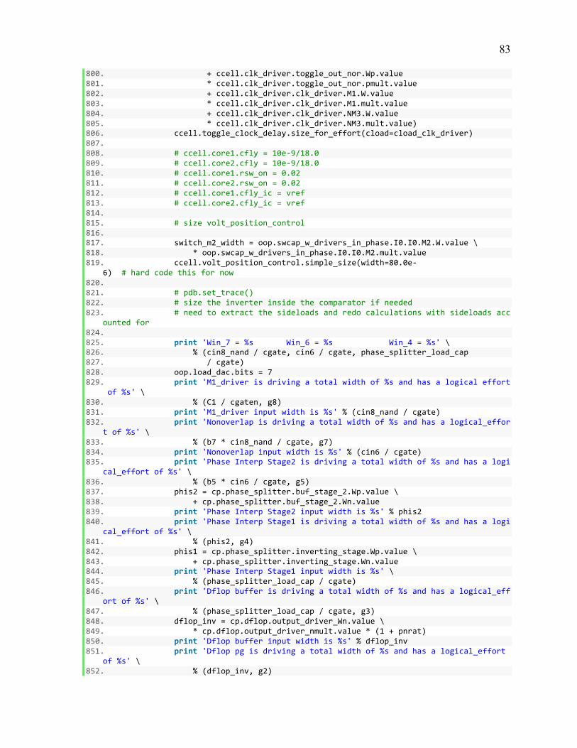
83
800. + ccell.clk_driver.toggle_out_nor.Wp.value 801. * ccell.clk_driver.toggle_out_nor.pmult.value 802. + ccell.clk_driver.clk_driver.M1.W.value 803. * ccell.clk_driver.clk_driver.M1.mult.value 804. + ccell.clk_driver.clk_driver.NM3.W.value 805. * ccell.clk_driver.clk_driver.NM3.mult.value) 806. ccell.toggle_clock_delay.size_for_effort(cload=cload_clk_driver) 807. 808. # ccell.core1.cfly = 10e-‐9/18.0 809. # ccell.core2.cfly = 10e-‐9/18.0 810. # ccell.core1.rsw_on = 0.02 811. # ccell.core2.rsw_on = 0.02 812. # ccell.core1.cfly_ic = vref 813. # ccell.core2.cfly_ic = vref 814. 815. # size volt_position_control 816. 817. switch_m2_width = oop.swcap_w_drivers_in_phase.I0.I0.M2.W.value \ 818. * oop.swcap_w_drivers_in_phase.I0.I0.M2.mult.value 819. ccell.volt_position_control.simple_size(width=80.0e-‐
6) # hard code this for now 820. 821. # pdb.set_trace() 822. # size the inverter inside the comparator if needed 823. # need to extract the sideloads and redo calculations with sideloads acc
ounted for 824. 825. print 'Win_7 = %s Win_6 = %s Win_4 = %s' \ 826. % (cin8_nand / cgate, cin6 / cgate, phase_splitter_load_cap 827. / cgate) 828. oop.load_dac.bits = 7 829. print 'M1_driver is driving a total width of %s and has a logical effort
of %s' \ 830. % (C1 / cgaten, g8) 831. print 'M1_driver input width is %s' % (cin8_nand / cgate) 832. print 'Nonoverlap is driving a total width of %s and has a logical_effor
t of %s' \ 833. % (b7 * cin8_nand / cgate, g7) 834. print 'Nonoverlap input width is %s' % (cin6 / cgate) 835. print 'Phase Interp Stage2 is driving a total width of %s and has a logi
cal_effort of %s' \ 836. % (b5 * cin6 / cgate, g5) 837. phis2 = cp.phase_splitter.buf_stage_2.Wp.value \ 838. + cp.phase_splitter.buf_stage_2.Wn.value 839. print 'Phase Interp Stage2 input width is %s' % phis2 840. print 'Phase Interp Stage1 is driving a total width of %s and has a logi
cal_effort of %s' \ 841. % (phis2, g4) 842. phis1 = cp.phase_splitter.inverting_stage.Wp.value \ 843. + cp.phase_splitter.inverting_stage.Wn.value 844. print 'Phase Interp Stage1 input width is %s' \ 845. % (phase_splitter_load_cap / cgate) 846. print 'Dflop buffer is driving a total width of %s and has a logical_eff
ort of %s' \ 847. % (phase_splitter_load_cap / cgate, g3) 848. dflop_inv = cp.dflop.output_driver_Wn.value \ 849. * cp.dflop.output_driver_nmult.value * (1 + pnrat) 850. print 'Dflop buffer input width is %s' % dflop_inv 851. print 'Dflop pg is driving a total width of %s and has a logical_effort
of %s' \ 852. % (dflop_inv, g2)

84
853. 854. # dflop_inv = cp.dflop.output_driver_Wn.value*(1+pnrat) 855. 856. print 'Dflop pg input width is %s' % (dflop_load_cap / cgate) 857. print 'comparator gate should be driving a Dflop pg input of %s' \ 858. % (cin1 / cgate * self.target_effort) 859. 860. # pdb.set_trace() 861. 862. self.fix_widths()
A.2 BAG PyCell Code This section contains PyCell code for examples of several different layout styles.
A.2.1 5 Transistor Amplifier PyCell
1. #!/usr/bin/python 2. # -‐*-‐ coding: utf-‐8 -‐*-‐ 3. from __future__ import with_statement 4. 5. __version__ = '$Revision: #1 $' 6. __author__ = 'John Crossley' 7. 8. from BAG_layout import * 9. import pdb 10. from operator import itemgetter 11. import inspect 12. 13. 14. class simple_amp(std_cell): 15. 16. ''''' 17. ''' 18. 19. paramNames = dict(L='L', Wn='Wn', Wp='Wp', Wtail='Wtail', 20. tail_height_ratio='tail_height_ratio') 21. 22. # types: 'rail', 'route_group' (NORTH to SOUTH list of ordered groups), route, devi
ce_row, device 23. 24. layout_info = [ # shared_source, shared_drain, series, parallel 25. # 'enforce_even_fingers' : True, # 26. { 27. 'name': 'VDD', 28. 'type': 'rail', 29. 'layer': 'metal1', 30. 'terminal': 'VDD', 31. 'term_type': 'INPUT_OUTPUT', 32. 'contact_to': 'diffusion', 33. 'enclose_contact': ['nimplant', 'nwell'], 34. }, 35. { 36. 'name': 'p_row1', 37. 'type': 'device_group', 38. 'tran_type': 'pmos', 39. 'height_ratio': None, 40. 'vertical_align': 'SOUTH', 41. 'subelements': [{

85
42. 'name': 'Mpmos', 43. 'param_mapping': {'W': 'Wp', 'L': 'L'}, 44. 'G': ['OUTN', 'OUTN'], 45. 'D': ['OUTN', 'OUTP'], 46. 'S': ['VDD'], 47. 'B': ['VDD'], 48. 'layout_type': 'shared_source', 49. 'align_position': 'CENTER', 50. 'align_point': 1, 51. }], 52. }, 53. {'name': 'route_group1', 'type': 'route_group', 54. 'subelements': [{ 55. 'name': 'OUTN', 56. 'layer': 'metal1', 57. 'terminal': None, 58. 'term_type': None, 59. }, { 60. 'name': 'OUTP', 61. 'layer': 'metal1', 62. 'terminal': 'OUTP', 63. 'term_type': 'OUTPUT', 64. }]}, 65. { 66. 'name': 'n_row1', 67. 'type': 'device_group', 68. 'tran_type': 'nmos', 69. 'height_ratio': None, 70. 'vertical_align': 'NORTH', 71. 'subelements': [{ 72. 'name': 'Mnmos', 73. 'param_mapping': {'W': 'Wn', 'L': 'L'}, 74. 'G': ['INP', 'INN'], 75. 'D': ['OUTN', 'OUTP'], 76. 'S': ['source'], 77. 'B': ['GND'], 78. 'layout_type': 'shared_source', 79. 'align_position': 'CENTER', 80. 'align_point': 1, 81. }], 82. }, 83. {'name': 'route_group2', 'type': 'route_group', 84. 'subelements': [{ 85. 'name': 'INN', 86. 'layer': 'metal1', 87. 'terminal': 'INN', 88. 'term_type': 'INPUT', 89. }, { 90. 'name': 'INP', 91. 'layer': 'metal1', 92. 'terminal': 'INP', 93. 'term_type': 'INPUT', 94. }, { 95. 'name': 'source', 96. 'layer': 'metal1', 97. 'terminal': None, 98. 'term_type': None, 99. }, { 100. 'name': 'BIAS', 101. 'layer': 'metal1', 102. 'terminal': 'BIAS',

86
103. 'term_type': 'INPUT', 104. }]}, 105. { 106. 'name': 'n_row2', 107. 'type': 'device_group', 108. 'tran_type': 'nmos', 109. 'height_ratio': 'tail_height_ratio', 110. 'vertical_align': 'NORTH', 111. 'subelements': [{ 112. 'name': 'Mtail', 113. 'param_mapping': {'W': 'Wtail', 'L': 'L'}, 114. 'G': ['BIAS'], 115. 'D': ['source'], 116. 'S': ['GND'], 117. 'B': ['GND'], 118. 'layout_type': 'single', 119. 'align_position': 'CENTER', 120. 'align_point': 1, 121. }], 122. }, 123. { 124. 'name': 'GND', 125. 'type': 'rail', 126. 'layer': 'metal1', 127. 'terminal': 'GND', 128. 'term_type': 'INPUT_OUTPUT', 129. 'contact_to': 'diffusion', 130. 'enclose_contact': ['pimplant'], 131. }, 132. ] 133. 134. default = dict(Wn=1.0, nmos_ratio=0.64, verticalPitch=10.2, 135. extra_rail_space_bottom=0.12) 136. 137. # ################################################################### 138. 139. @classmethod 140. def defineParamSpecs(cls, specs): 141. """Define the PyCell parameters. The order of invocation of 142. specs() becomes the order on the form. 143. 144. Arguments: 145. specs -‐ (ParamSpecArray) PyCell parameters 146. 147. These are the parameters in the paramNames dictionary -‐
define them here 148. """ 149. 150. [selfcopy, hlink] = printmeth(cls) 151. 152. # Super makes all the parent functions available in the new defineParamS
pecs 153. 154. super(simple_amp, cls).defineParamSpecs(specs) 155. mySpecs = ParamSpecArray() 156. 157. # Set up specs 158. 159. L = specs.tech.getMosfetParams('nmos', cls.oxide, 'minLength') # minimu
m length (get from tech file) 160. L = cls.grid.snap(L) # snap to grid

87
161. 162. # stepConstraint = starting value, step size, and resolution (maybe numb
er of points?) or max value 163. 164. stepConstraint = StepConstraint(cls.maskgrid, start=L, 165. resolution=cls.resolution, action=FailAction.REJECT) 166. 167. # myspecs: (name, (default OR L you've defined), constraint) 168. 169. mySpecs('L', cls.default.get('L', L), constraint=stepConstraint) 170. 171. Wn = specs.tech.getMosfetParams('nmos', cls.oxide, 'minWidth') 172. Wn = cls.grid.snap(Wn) 173. stepConstraint = StepConstraint(cls.maskgrid, start=Wn, 174. resolution=cls.resolution, action=FailAction.REJECT) 175. mySpecs('Wn', cls.default.get('Wn', Wn), 176. constraint=stepConstraint) 177. mySpecs('Wp', cls.default.get('Wp', Wn), 178. constraint=stepConstraint) 179. mySpecs('Wtail', cls.default.get('Wtail', Wn), 180. constraint=stepConstraint) 181. mySpecs('tail_height_ratio', 0.25) 182. 183. # Parameter renaming: adds mySpecs (what you've defined above) into spec
s 184. 185. renameParams(mySpecs, specs, cls.paramNames) 186. 187. # This is a Debugging call and should ALWAYS be the last line of a metho
d 188. 189. savemeth(cls, selfcopy, hlink) 190. 191. # ################################################################### 192. 193. def define_derived_parameters(self): 194. ''''' 195. Any derived parameters that are referenced in self.layout_info should be
defined here 196. 197. For example, in the pmos device_group below the param_mapping of 'W' is
'Wp'. If Wp is not a 198. parameter defined at the pycell level, then self.Wp must be defined in t
his function. 199. 200. 'subelements' : [ { 'name':'M3M4',
201. 'param_mapping': {'W':'Wp' }, 202. 'G' : ['IN1','IN2'], 203. 'D' : ['OUT'], 204. 'S' : ['VDD'], 205. 'B' : ['VDD'], 206. 'layout_type' : 'series' #sh
ared_source, shared_drain, series, parallel 207. }, 208. 209. def define_derived_parameters(self) : 210. self.Wp = self.grid.snap(self.PNratio*self.Wn) 211. 212. Basically, the contents of params get turned into fields, so here you sh
ould add any derived parameters as fields if they

88
213. don't appear in params 214. ''' 215. 216. [selfcopy, hlink] = printmeth(self) 217. 218. # This is a Debugging call and should ALWAYS be the last line of a metho
d 219. 220. savemeth(self, selfcopy, hlink)
A.2.2 Asynchronous Comparator
1. #!/usr/bin/python 2. # -‐*-‐ coding: utf-‐8 -‐*-‐ 3. from __future__ import with_statement 4. 5. __version__ = '$Revision: #1 $' 6. __author__ = 'John Crossley' 7. 8. from BAG_layout import * 9. import pdb 10. from operator import itemgetter 11. 12. 13. class async_comp(std_cell_row): 14. 15. ''''' 16. This is a new version of the async_comp that inherits from std_cell_row 17. ''' 18. 19. paramNames = dict( 20. L='L', 21. input_width='input_width', 22. mult_input_mirror='mult_input_mirror', 23. bias_enable_width='bias_enable_width', 24. mult_bias_enable_mirror='mult_bias_enable_mirror', 25. bias_width='bias_width', 26. mult_input='mult_input', 27. mult_precharge='mult_precharge', 28. mult_bias_mirror='mult_bias_mirror', 29. mult_bias_enable='mult_bias_enable', 30. mult_bias='mult_bias', 31. inv_feedback_width='inv_feedback_width', 32. mult_feedback='mult_feedback', 33. inv_n_width='inv_n_width', 34. inv_p_width='inv_p_width', 35. inv2_n_width='inv2_n_width', 36. inv2_p_width='inv2_p_width', 37. inv_en_n_width='inv_en_n_width', 38. inv_en_p_width='inv_en_p_width', 39. extra_vertical_pitch_vref='extra_vertical_pitch_vref', 40. decap_p_width='decap_p_width', 41. decap_length='decap_length', 42. decap_n_width='decap_n_width', 43. decap_n_type='decap_n_type', 44. decap_p_type='decap_p_type', 45. ) 46. 47. # types: 'route_group' (WEST to EAST list of ordered routes), route, std_cell, std
_cell_row

89
48. 49. pin_info = [{ 50. 'name': 'VREF', 51. 'term_type': 'INPUT_OUTPUT', 52. 'subelements': [{'instance': 'async_comp_p1', 'terminal': 'VDD' 53. }, {'instance': 'M_bias_decouple', 54. 'terminal': 'VDD'}, 55. {'instance': 'M_bias_decouple_VREF_GND', 56. 'terminal': 'VDD'}], 57. 'type': 'rail', 58. }, { 59. 'name': 'VDD', 60. 'term_type': 'INPUT_OUTPUT', 61. 'subelements': [{'instance': 'async_comp_p2', 'terminal': 'VDD' 62. }, {'instance': 'async_comp_p3', 63. 'terminal': 'VDD'}], 64. 'type': 'rail', 65. }, { 66. 'name': 'GND', 67. 'term_type': 'INPUT_OUTPUT', 68. 'subelements': [{'instance': 'M_bias_decouple_VREF_GND', 69. 'terminal': 'GND'}, 70. {'instance': 'M_bias_decouple', 71. 'terminal': 'GND'}, {'instance': 'async_comp_p1' 72. , 'terminal': 'GND'}, 73. {'instance': 'async_comp_p2', 'terminal': 'GND' 74. }, {'instance': 'async_comp_p3', 75. 'terminal': 'GND'}], 76. 'type': 'rail', 77. }] 78. 79. layout_info = [ # extra space on left and right of this routing group (in um) 80. # {'name': 'con_vref', 'layer':'metal', 'terminal': None, 'term_ty
pe': None }, 81. # extra space on left and right of this routing group (in um) 82. # 83. # extra space on left and right of this routing group (in um) 84. # {'name': 'int', 'layer':'metal2', 'terminal': None, 'term_type':
None }, 85. # extra space on left and right of this routing group (in um) 86. # 'mirror_y' : 'True', 87. # extra space on left and right of this routing group (in um) 88. # 'mirror_y' : 'True', 89. # extra space on left and right of this routing group (in um) 90. # extra space on left and right of this routing group (in um) 91. { 92. 'name': 'M_bias_decouple_VREF_GND', 93. 'type': 'std_cell', 94. 'lib_cell': 'BAG_std_cells_oa/cap_decouple', 95. 'param_mapping': { 96. 'Wn': 'decap_n_width', 97. 'Wp': 'decap_p_width', 98. 'L': 'decap_length', 99. 'extra_vertical_pitch_top': 'extra_vertical_pitch_vref' 100. , 101. 'verticalPitch': 'p1_verticalPitch', 102. 'extend_enclosing_layers_to_pr': 'extend_enclosing_layers_pmos_c
ap' 103. , 104. 'device_type_nmos': 'decap_n_type', 105. 'device_type_pmos': 'decap_p_type',

90
106. 'extra_space_for_thick_ox': 'extra_space_for_thick_ox', 107. }, 108. 'pin_mapping': {'VDD': 'con_vref', 'GND': 'GND'}, 109. }, 110. { 111. 'name': 'route_groupm1', 112. 'type': 'route_group', 113. 'extra_space': 0.4, 114. 'subelements': [{ 115. 'name': 'bias', 116. 'layer': 'metal2', 117. 'terminal': None, 118. 'term_type': None, 119. }], 120. }, 121. { 122. 'name': 'M_bias_decouple', 123. 'type': 'std_cell', 124. 'lib_cell': 'BAG_std_cells_oa/async_cap_decouple', 125. 'param_mapping': { 126. 'Wn': 'decap_n_width', 127. 'Wp': 'decap_p_width', 128. 'L': 'decap_length', 129. 'extra_vertical_pitch_top': 'extra_vertical_pitch_vref' 130. , 131. 'verticalPitch': 'p1_verticalPitch', 132. 'extend_enclosing_layers_to_pr': 'extend_enclosing_layers_pmos_c
ap' 133. , 134. 'device_type_nmos': 'decap_n_type', 135. 'device_type_pmos': 'decap_p_type', 136. 'extra_space_for_thick_ox': 'extra_space_for_thick_ox', 137. }, 138. 'pin_mapping': { 139. 'VDD': 'con_vref', 140. 'comp_bias': 'bias', 141. 'comp_bias_global': 'bias2', 142. 'GND': 'GND', 143. }, 144. }, 145. { 146. 'name': 'route_group0', 147. 'type': 'route_group', 148. 'extra_space': 0.2, 149. 'subelements': [{ 150. 'name': 'bias', 151. 'layer': 'metal2', 152. 'terminal': None, 153. 'term_type': None, 154. }, { 155. 'name': 'bias2', 156. 'layer': 'metal2', 157. 'terminal': None, 158. 'term_type': None, 159. }, { 160. 'name': 'con_vref', 161. 'layer': 'metal1', 162. 'terminal': None, 163. 'term_type': None, 164. }], 165. },

91
166. { 167. 'name': 'async_comp_p1', 168. 'type': 'std_cell', 169. 'lib_cell': 'BAG_std_cells_oa/async_comp_p1', 170. 'param_mapping': { 171. 'input_width': 'input_width', 172. 'mult_input_mirror': 'mult_input_mirror', 173. 'bias_enable_width': 'bias_enable_width', 174. 'mult_bias_enable_mirror': 'mult_bias_enable_mirror', 175. 'bias_width': 'bias_width', 176. 'mult_bias_mirror': 'mult_bias_mirror', 177. 'extra_vertical_pitch_top': 'extra_vertical_pitch_vref' 178. , 179. 'verticalPitch': 'p1_verticalPitch', 180. 'extend_enclosing_layers_to_pr': 'extend_enclosing_layers_pmos_c
ap' 181. , 182. }, 183. 'pin_mapping': { 184. 'bias': 'bias', 185. 'bias2': 'bias2', 186. 'vref_in': 'con_vref', 187. 'VDD': 'con_vref', 188. 'GND': 'GND', 189. }, 190. }, 191. { 192. 'name': 'route_group1', 193. 'type': 'route_group', 194. 'extra_space': 0.2, 195. 'subelements': [{ 196. 'name': 'bias', 197. 'layer': 'metal2', 198. 'terminal': 'bias', 199. 'term_type': 'INPUT_OUTPUT', 200. 'extra_space': 0.0, 201. }, { 202. 'name': 'bias2', 203. 'layer': 'metal2', 204. 'terminal': 'bias2', 205. 'term_type': 'INPUT_OUTPUT', 206. 'extra_space': 0.0, 207. }], 208. }, 209. { 210. 'name': 'async_comp_p2', 211. 'type': 'std_cell', 212. 'lib_cell': 'BAG_std_cells_oa/async_comp_p2', 213. 'param_mapping': { 214. 'input_width': 'input_width', 215. 'mult_input': 'mult_input', 216. 'mult_precharge': 'mult_precharge', 217. 'bias_enable_width': 'bias_enable_width', 218. 'mult_bias_enable': 'mult_bias_enable', 219. 'bias_width': 'bias_width', 220. 'mult_bias': 'mult_bias', 221. 'share_nwell_left': 'share_nwell_left_p2', 222. 'extend_enclosing_layers_to_pr': 'extend_enclosing_layers_to_pr_
p2' 223. , 224. },

92
225. 'pin_mapping': { 226. 'bias': 'bias', 227. 'bias2': 'bias2', 228. 'VDD': 'VDD', 229. 'GND': 'GND', 230. 'enable': 'int_enable', 231. 'int': 'int', 232. }, 233. }, 234. { 235. 'name': 'route_group10', 236. 'type': 'route_group', 237. 'extra_space': 0.2, 238. 'subelements': [{ 239. 'name': 'int', 240. 'layer': 'metal2', 241. 'terminal': None, 242. 'term_type': None, 243. 'extra_space': 0.1, 244. }, { 245. 'name': 'int_enable', 246. 'layer': 'metal2', 247. 'terminal': 'int_enable', 248. 'term_type': 'INPUT_OUTPUT', 249. }], 250. }, 251. { 252. 'name': 'inv_enable_2', 253. 'type': 'std_cell', 254. 'lib_cell': 'BAG_std_cells_oa/Inverter_pass_through', 255. 'param_mapping': {'L': 'L', 'Wn': 'Wn_inv', 256. 'PNratio': 'pnrat_inv'}, 257. 'pin_mapping': { 258. 'IN': 'enable_b', 259. 'OUT': 'int_enable', 260. 'int': 'int', 261. 'VDD': 'VDD', 262. 'GND': 'GND', 263. }, 264. }, 265. { 266. 'name': 'route_group11', 267. 'type': 'route_group', 268. 'extra_space': 0.2, 269. 'subelements': [{ 270. 'name': 'enable_b', 271. 'layer': 'metal2', 272. 'terminal': None, 273. 'term_type': None, 274. }, { 275. 'name': 'int', 276. 'layer': 'metal2', 277. 'terminal': None, 278. 'term_type': None, 279. 'extra_space': 0.1, 280. }], 281. }, 282. { 283. 'name': 'inv_enable_1', 284. 'type': 'std_cell', 285. 'lib_cell': 'BAG_std_cells_oa/Inverter_pass_through',

93
286. 'param_mapping': {'L': 'L', 'Wn': 'Wn_inv', 287. 'PNratio': 'pnrat_inv'}, 288. 'pin_mapping': { 289. 'IN': 'enable', 290. 'OUT': 'enable_b', 291. 'int': 'int', 292. 'VDD': 'VDD', 293. 'GND': 'GND', 294. }, 295. }, 296. { 297. 'name': 'route_group12', 298. 'type': 'route_group', 299. 'extra_space': 0.2, 300. 'subelements': [{ 301. 'name': 'enable', 302. 'layer': 'metal2', 303. 'terminal': 'enable', 304. 'term_type': 'INPUT', 305. }, { 306. 'name': 'int', 307. 'layer': 'metal2', 308. 'terminal': 'internal_node', 309. 'term_type': 'INPUT_OUTPUT', 310. 'extra_space': 0.1, 311. }], 312. }, 313. { 314. 'name': 'async_comp_p3', 315. 'type': 'std_cell', 316. 'lib_cell': 'BAG_std_cells_oa/async_comp_p3_v2', 317. 'param_mapping': { 318. 'inv_feedback_width': 'inv_feedback_width', 319. 'mult_feedback': 'mult_feedback', 320. 'inv_n_width': 'inv_n_width', 321. 'inv_p_width': 'inv_p_width', 322. 'inv2_n_width': 'inv2_n_width', 323. 'inv2_p_width': 'inv2_p_width', 324. }, 325. 'pin_mapping': { 326. 'VDD': 'VDD', 327. 'GND': 'GND', 328. 'out': 'out', 329. 'in': 'int', 330. }, 331. }, 332. { 333. 'name': 'route_group_out', 334. 'type': 'route_group', 335. 'extra_space': 0.2, 336. 'subelements': [{ 337. 'name': 'out', 338. 'layer': 'metal2', 339. 'terminal': 'out', 340. 'term_type': 'OUTPUT', 341. }], 342. }, 343. ] 344. 345. default = dict(Wn=0.4, nmos_ratio=0.45, PNRatio=2.0, 346. verticalPitch=5.0, railWidth=0.36)
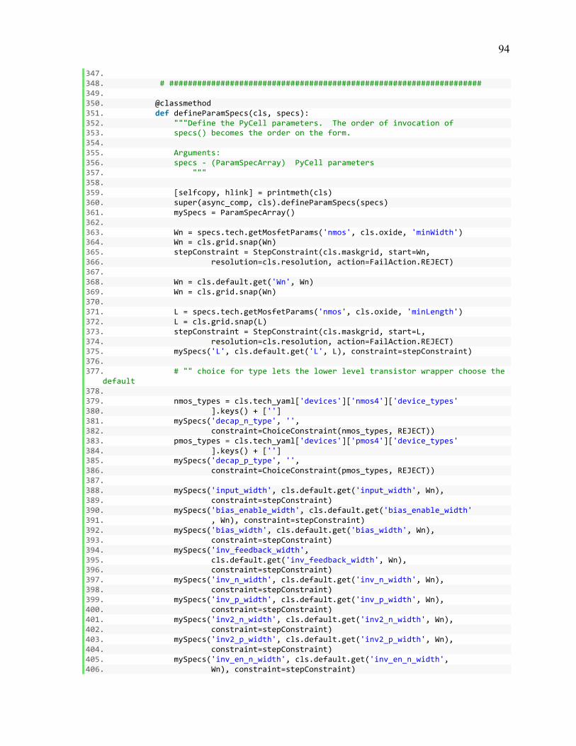
94
347. 348. # ################################################################### 349. 350. @classmethod 351. def defineParamSpecs(cls, specs): 352. """Define the PyCell parameters. The order of invocation of 353. specs() becomes the order on the form. 354. 355. Arguments: 356. specs -‐ (ParamSpecArray) PyCell parameters 357. """ 358. 359. [selfcopy, hlink] = printmeth(cls) 360. super(async_comp, cls).defineParamSpecs(specs) 361. mySpecs = ParamSpecArray() 362. 363. Wn = specs.tech.getMosfetParams('nmos', cls.oxide, 'minWidth') 364. Wn = cls.grid.snap(Wn) 365. stepConstraint = StepConstraint(cls.maskgrid, start=Wn, 366. resolution=cls.resolution, action=FailAction.REJECT) 367. 368. Wn = cls.default.get('Wn', Wn) 369. Wn = cls.grid.snap(Wn) 370. 371. L = specs.tech.getMosfetParams('nmos', cls.oxide, 'minLength') 372. L = cls.grid.snap(L) 373. stepConstraint = StepConstraint(cls.maskgrid, start=L, 374. resolution=cls.resolution, action=FailAction.REJECT) 375. mySpecs('L', cls.default.get('L', L), constraint=stepConstraint) 376. 377. # "" choice for type lets the lower level transistor wrapper choose the
default 378. 379. nmos_types = cls.tech_yaml['devices']['nmos4']['device_types' 380. ].keys() + [''] 381. mySpecs('decap_n_type', '', 382. constraint=ChoiceConstraint(nmos_types, REJECT)) 383. pmos_types = cls.tech_yaml['devices']['pmos4']['device_types' 384. ].keys() + [''] 385. mySpecs('decap_p_type', '', 386. constraint=ChoiceConstraint(pmos_types, REJECT)) 387. 388. mySpecs('input_width', cls.default.get('input_width', Wn), 389. constraint=stepConstraint) 390. mySpecs('bias_enable_width', cls.default.get('bias_enable_width' 391. , Wn), constraint=stepConstraint) 392. mySpecs('bias_width', cls.default.get('bias_width', Wn), 393. constraint=stepConstraint) 394. mySpecs('inv_feedback_width', 395. cls.default.get('inv_feedback_width', Wn), 396. constraint=stepConstraint) 397. mySpecs('inv_n_width', cls.default.get('inv_n_width', Wn), 398. constraint=stepConstraint) 399. mySpecs('inv_p_width', cls.default.get('inv_p_width', Wn), 400. constraint=stepConstraint) 401. mySpecs('inv2_n_width', cls.default.get('inv2_n_width', Wn), 402. constraint=stepConstraint) 403. mySpecs('inv2_p_width', cls.default.get('inv2_p_width', Wn), 404. constraint=stepConstraint) 405. mySpecs('inv_en_n_width', cls.default.get('inv_en_n_width', 406. Wn), constraint=stepConstraint)

95
407. mySpecs('inv_en_p_width', cls.default.get('inv_en_p_width', 408. Wn), constraint=stepConstraint) 409. mySpecs('decap_n_width', cls.default.get('decap_n_width', 10 410. * Wn), constraint=stepConstraint) 411. mySpecs('decap_p_width', cls.default.get('decap_p_width', 10 412. * Wn), constraint=stepConstraint) 413. mySpecs('decap_length', cls.default.get('decap_length', 10 414. * L), constraint=stepConstraint) 415. 416. mySpecs('mult_feedback', cls.default.get('mult_feedback', 2), 417. constraint=StepConstraint(1, start=1, 418. action=FailAction.REJECT)) 419. mySpecs('mult_input_mirror', cls.default.get('mult_input_mirror' 420. , 2), constraint=StepConstraint(1, start=1, 421. action=FailAction.REJECT)) 422. mySpecs('mult_bias_enable_mirror', 423. cls.default.get('mult_bias_enable_mirror', 2), 424. constraint=StepConstraint(1, start=1, 425. action=FailAction.REJECT)) 426. mySpecs('mult_bias_mirror', cls.default.get('mult_bias_mirror', 427. 2), constraint=StepConstraint(1, start=1, 428. action=FailAction.REJECT)) 429. mySpecs('mult_input', cls.default.get('mult_input', 2), 430. constraint=StepConstraint(1, start=1, 431. action=FailAction.REJECT)) 432. mySpecs('mult_precharge', cls.default.get('mult_precharge', 2), 433. constraint=StepConstraint(1, start=1, 434. action=FailAction.REJECT)) 435. mySpecs('mult_bias_enable', cls.default.get('mult_bias_enable', 436. 2), constraint=StepConstraint(1, start=1, 437. action=FailAction.REJECT)) 438. mySpecs('mult_bias', cls.default.get('mult_bias', 2), 439. constraint=StepConstraint(1, start=1, 440. action=FailAction.REJECT)) 441. mySpecs('extra_vertical_pitch_vref', 0.0, 442. constraint=RangeConstraint(0.0, None, 443. action=FailAction.REJECT)) 444. 445. # Parameter renaming 446. 447. renameParams(mySpecs, specs, cls.paramNames) 448. 449. # This is a Debugging call and should ALWAYS be the last line of a metho
d 450. 451. savemeth(cls, selfcopy, hlink) 452. 453. # ################################################################### 454. 455. def define_derived_parameters(self): 456. ''''' 457. Any derived parameters that are referenced in self.layout_info should be
defined here 458. 459. For example, in the pmos device_group below the param_mapping of 'W' is
'Wp'. If Wp is not a 460. parameter defined a the pycell level, then self.Wp must be defined in th
is function. 461. 462. 'subelements' : [ { 'name':'M3M4',
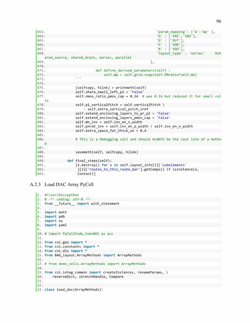
96
463. 'param_mapping': {'W':'Wp' }, 464. 'G' : ['IN1','IN2'], 465. 'D' : ['OUT'], 466. 'S' : ['VDD'], 467. 'B' : ['VDD'], 468. 'layout_type' : 'series' #sh
ared_source, shared_drain, series, parallel 469. }, 470. 471. def define_derived_parameters(self) : 472. self.Wp = self.grid.snap(self.PNratio*self.Wn) 473. ''' 474. 475. [selfcopy, hlink] = printmeth(self) 476. self.share_nwell_left_p2 = 'False' 477. self.nmos_ratio_pmos_cap = 0.24 # was 0.16 but reduced it for small cel
ls 478. self.p1_verticalPitch = self.verticalPitch \ 479. -‐ self.extra_vertical_pitch_vref 480. self.extend_enclosing_layers_to_pr_p2 = 'False' 481. self.extend_enclosing_layers_pmos_cap = 'False' 482. self.Wn_inv = self.inv_en_n_width 483. self.pnrat_inv = self.inv_en_p_width / self.inv_en_n_width 484. self.extra_space_for_thick_ox = 0.4 485. 486. # This is a Debugging call and should ALWAYS be the last line of a metho
d 487. 488. savemeth(self, selfcopy, hlink) 489. 490. def final_steps(self): 491. [x.destroy() for x in self.layout_info[3]['subelements' 492. ][2]['routes_to_this_route_bar'].getComps() if isinstance(x, 493. Contact)]
A.2.3 Load DAC Array PyCell
1. #!/usr/bin/python 2. # -‐*-‐ coding: utf-‐8 -‐*-‐ 3. from __future__ import with_statement 4. 5. import math 6. import pdb 7. import os 8. import yaml 9. 10. # import PyCellCode_tsmcN65 as pcc 11. 12. from cni.geo import * 13. from cni.constants import * 14. from cni.dlo import * 15. from BAG_layout.ArrayMethods import ArrayMethods 16. 17. # from demo_cells.ArrayMethods import ArrayMethods 18. 19. from cni.integ.common import createInstances, renameParams, \ 20. reverseDict, stretchHandle, Compare 21. 22. 23. class load_dac(ArrayMethods):

97
24. 25. """Define the PyCell class. 26. """ 27. 28. paramNames = dict( 29. W_n='W_n', 30. L_n='L_n', 31. pwr_width_horiz='pwr_width_horiz', 32. pwr_width_vert='pwr_width_vert', 33. drain_width='drain_width', 34. rc_width='rc_width', 35. nmos_ratio='nmos_ratio', 36. verticalPitch='verticalPitch', 37. mirrorx='mirrorx', 38. mirrory='mirrory', 39. ) 40. 41. default = dict( 42. bits=4, 43. mirrorx='true', 44. mirrory='false', 45. pwr_width_horiz=0.8, 46. pwr_width_vert=0.8, 47. verticalPitch=2.2, 48. W_n=1.2, 49. L_n=.06, 50. nmos_ratio=.74, 51. ) 52. 53. oxide = 'thin' 54. 55. # Unit cell name 56. 57. cell_name = 'BAG_std_cells_oa/load_dac_ucell/layout' 58. 59. @classmethod 60. def defineParamSpecs(cls, specs): 61. """ Define the PyCell parameters. 62. """ 63. 64. super(load_dac, cls).defineParamSpecs(specs) 65. minmetal1 = float(specs.tech.getPhysicalRule('minWidth', 66. cls.layer['metal1'])) 67. maskgrid = specs.tech.getGridResolution() 68. cls.specs = specs 69. cls.tech = specs.tech 70. 71. cls.maskgrid = specs.tech.getGridResolution() 72. cls.resolution = specs.tech.uu2dbu(1) * 10 73. cls.grid = Grid(cls.maskgrid, snapType=SnapType.ROUND) 74. 75. mySpecs = ParamSpecArray() 76. 77. Wmin_nmos = specs.tech.getMosfetParams('nmos', cls.oxide, 78. 'minWidth') 79. Wmin_pmos = specs.tech.getMosfetParams('pmos', cls.oxide, 80. 'minWidth') 81. 82. Lmin_nmos = specs.tech.getMosfetParams('nmos', cls.oxide, 83. 'minLength') 84. Lmin_pmos = specs.tech.getMosfetParams('pmos', cls.oxide,

98
85. 'minLength') 86. 87. W_n = Wmin_nmos 88. W_n = cls.grid.snap(W_n) 89. stepConstraint = StepConstraint(cls.maskgrid, start=W_n, 90. resolution=cls.resolution, action=FailAction.REJECT) 91. mySpecs('W_n', cls.default.get('W_n', W_n), 92. constraint=stepConstraint) 93. 94. L_n = Lmin_nmos 95. L_n = cls.grid.snap(L_n) 96. stepConstraint = StepConstraint(cls.maskgrid, start=L_n, 97. resolution=cls.resolution, action=FailAction.REJECT) 98. mySpecs('L_n', cls.default.get('L_n', L_n), 99. constraint=stepConstraint) 100. 101. pwr_width_horiz = float(cls.default.get('pwr_width_horiz', -‐1)) 102. pwr_width_horiz_constraint = RangeConstraint(0.1, 10.0, 103. action=FailAction.REJECT) 104. mySpecs('pwr_width_horiz', pwr_width_horiz, 105. constraint=pwr_width_horiz_constraint) 106. 107. pwr_width_vert = float(cls.default.get('pwr_width_vert', -‐1)) 108. pwr_width_vert_constraint = RangeConstraint(0.1, 10.0, 109. action=FailAction.REJECT) # TODO: this shoudn't be hard coded 110. specs('pwr_width_vert', pwr_width_vert, 111. constraint=pwr_width_vert_constraint) 112. 113. rc_width = float(cls.default.get('rc_width', 114. cls.metal_min_width[cls.layer['metal2']])) 115. rc_width_constraint = \ 116. RangeConstraint(cls.metal_min_width[cls.layer['metal2']], 117. 10.0, action=FailAction.REJECT) 118. specs('rc_width', rc_width, constraint=rc_width_constraint) 119. 120. drain_width = float(cls.default.get('drain_width', 121. cls.metal_min_width[cls.layer['metal2']])) 122. drain_width_constraint = \ 123. RangeConstraint(cls.metal_min_width[cls.layer['metal2']], 124. 10.0, action=FailAction.REJECT) 125. specs('drain_width', drain_width, 126. constraint=drain_width_constraint) 127. 128. nmos_ratio = cls.default.get('nmos_ratio', 0.42) 129. mySpecs('nmos_ratio', nmos_ratio, 130. constraint=RangeConstraint(0.01, 0.99, 131. action=FailAction.REJECT)) 132. 133. verticalPitch = cls.default.get('verticalPitch', 60.0 134. * minmetal1) 135. mySpecs('verticalPitch', verticalPitch, 136. constraint=StepConstraint(cls.maskgrid, 137. start=minmetal1, resolution=cls.resolution, 138. action=FailAction.REJECT)) 139. 140. renameParams(mySpecs, specs, cls.paramNames) 141. 142. def setupParams(self, params): 143. """ Do parameter checking. 144. """ 145.

99
146. super(load_dac, self).setupParams(params) 147. self.name_num = 0 148. self.max_iter = 50 149. self.bias_enable = False 150. 151. # self.max_dist = self.max_distance_from_bias 152. 153. def genTopology(self): 154. """ 155. """ 156. 157. # First, we must calculate the number of extra contacts needed to make e
ach cell 158. # mirrorable. 159. 160. params = ParamArray( 161. cell_intent='dummy', 162. pwr_width_horiz=self.pwr_width_horiz, 163. rc_width=self.rc_width, 164. drain_width=self.drain_width, 165. verticalPitch=self.verticalPitch, 166. W_n=self.W_n, 167. L_n=self.L_n, 168. ) 169. instance_data = self.make_unit_cells_mirrorable(self.cell_name, 170. params) 171. 172. # Save the transistor parameters as well 173. 174. self.result_props['cs_fing_width'] = \ 175. instance_data['M1_finger_width'] 176. self.result_props['cs_nf'] = instance_data['M1_num_fingers'] 177. 178. # Define connectivity for "normal" cells -‐
this will change for different designs! 179. 180. dummy_params = ParamArray( 181. cell_intent='dummy', 182. pwr_width_horiz=self.pwr_width_horiz, 183. rc_width=self.rc_width, 184. drain_width=self.drain_width, 185. verticalPitch=self.verticalPitch, 186. W_n=self.W_n, 187. L_n=self.L_n, 188. make_mirrorable='False', 189. extra_vdd_rail_contacts_right=self.extra_vdd_rail_contacts_right, 190. extra_gnd_rail_contacts_right=self.extra_gnd_rail_contacts_right, 191. extra_vdd_rail_contacts_left=self.extra_vdd_rail_contacts_left, 192. extra_gnd_rail_contacts_left=self.extra_gnd_rail_contacts_left, 193. ) 194. 195. prefixes = {'dummy': 'D', 'normal_even': 'I', 'normal_odd': 'I'} 196. 197. self.createArray(dummy_params, dummy_params, prefixes) # pass dummy_par
ams to bias_params but bias is disabled 198. 199. def connect_up_to_power_grid(self): 200. for hpin in self.horizontal_power_pins: 201. the_shape = hpin.getShapes()[0] 202. the_net = hpin.getTerm().getName() 203. m3_shape = Rect(self.layer['metal3'], the_shape.getBBox())

100
204. m5_shape = Rect(self.layer['metal5'], the_shape.getBBox()) 205. for vpin in self.vertical_power_pins: 206. if vpin.getTerm().getName() == the_net: 207. vshape = vpin.getShapes()[0] 208. overlap = vshape.fgAnd(the_shape, 209. self.layer['metal1']) 210. p1 = overlap.getBBox().lowerLeft() 211. p2 = overlap.getBBox().upperRight() 212. AbutContact( 213. vshape.getLayer(), 214. m5_shape.getLayer(), 215. routeDir1=NORTH_SOUTH, 216. routeDir2=EAST_WEST, 217. point1=p1, 218. point2=p2, 219. abutDir=EAST_WEST, 220. ) 221. overlap.destroy() 222. hpin.removeShape(the_shape) 223. hpin.addShape(m5_shape) 224. for vpin in self.vertical_power_pins: 225. the_shape = vpin.getShapes()[0] 226. the_net = vpin.getTerm().getName() 227. m6_shape = Rect(self.layer['metal6'], the_shape.getBBox()) 228. m7_shape = Rect(self.layer['metal7'], the_shape.getBBox()) 229. for hpin in self.horizontal_power_pins: 230. if hpin.getTerm().getName() == the_net: 231. hshape = hpin.getShapes()[0] 232. overlap = hshape.fgAnd(the_shape, 233. self.layer['metal1']) 234. p1 = overlap.getBBox().lowerLeft() 235. p2 = overlap.getBBox().upperRight() 236. AbutContact( 237. hshape.getLayer(), 238. m6_shape.getLayer(), 239. routeDir1=EAST_WEST, 240. routeDir2=NORTH_SOUTH, 241. point1=p1, 242. point2=p2, 243. abutDir=EAST_WEST, 244. ) 245. overlap.destroy() 246. p1 = m6_shape.getBBox().lowerLeft() 247. p2 = m6_shape.getBBox().upperRight() 248. AbutContact( 249. m7_shape.getLayer(), 250. m6_shape.getLayer(), 251. routeDir1=NORTH_SOUTH, 252. routeDir2=NORTH_SOUTH, 253. point1=p1, 254. point2=p2, 255. abutDir=NORTH_SOUTH, 256. ) 257. vpin.removeShape(the_shape) 258. vpin.addShape(m7_shape) 259. for hpin in self.horizontal_power_pins: 260. hpin.destroy() 261. del self.horizontal_power_pins 262. 263. def genLayout(self): 264. """ Construct the PyCell geometries.
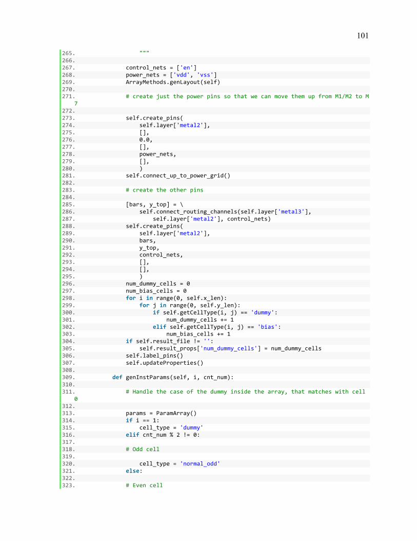
101
265. """ 266. 267. control_nets = ['en'] 268. power_nets = ['vdd', 'vss'] 269. ArrayMethods.genLayout(self) 270. 271. # create just the power pins so that we can move them up from M1/M2 to M
7 272. 273. self.create_pins( 274. self.layer['metal2'], 275. [], 276. 0.0, 277. [], 278. power_nets, 279. [], 280. ) 281. self.connect_up_to_power_grid() 282. 283. # create the other pins 284. 285. [bars, y_top] = \ 286. self.connect_routing_channels(self.layer['metal3'], 287. self.layer['metal2'], control_nets) 288. self.create_pins( 289. self.layer['metal2'], 290. bars, 291. y_top, 292. control_nets, 293. [], 294. [], 295. ) 296. num_dummy_cells = 0 297. num_bias_cells = 0 298. for i in range(0, self.x_len): 299. for j in range(0, self.y_len): 300. if self.getCellType(i, j) == 'dummy': 301. num_dummy_cells += 1 302. elif self.getCellType(i, j) == 'bias': 303. num_bias_cells += 1 304. if self.result_file != '': 305. self.result_props['num_dummy_cells'] = num_dummy_cells 306. self.label_pins() 307. self.updateProperties() 308. 309. def genInstParams(self, i, cnt_num): 310. 311. # Handle the case of the dummy inside the array, that matches with cell
0 312. 313. params = ParamArray() 314. if i == 1: 315. cell_type = 'dummy' 316. elif cnt_num % 2 != 0: 317. 318. # Odd cell 319. 320. cell_type = 'normal_odd' 321. else: 322. 323. # Even cell

102
324. 325. cell_type = 'normal_even' 326. params = ParamArray( 327. cell_intent=cell_type, 328. pwr_width_horiz=self.pwr_width_horiz, 329. pwr_width_vert=self.pwr_width_vert, 330. rc_width=self.rc_width, 331. drain_width=self.drain_width, 332. verticalPitch=self.verticalPitch, 333. W_n=self.W_n, 334. L_n=self.L_n, 335. make_mirrorable='False', 336. extra_vdd_rail_contacts_right=self.extra_vdd_rail_contacts_right, 337. extra_gnd_rail_contacts_right=self.extra_gnd_rail_contacts_right, 338. extra_vdd_rail_contacts_left=self.extra_vdd_rail_contacts_left, 339. extra_gnd_rail_contacts_left=self.extra_gnd_rail_contacts_left, 340. ) 341. return [cell_type, params]
A.2.4 Control Core
1. #!/usr/bin/python 2. # -‐*-‐ coding: utf-‐8 -‐*-‐ 3. from __future__ import with_statement 4. 5. from BAG_layout import * 6. import pdb 7. from operator import itemgetter 8. 9. # comp_core3.py vs comp_core2.py -‐ comp_core3 moves the level shifter caps 10. # (pmos in isolated nwells) into the control 11. # core cell and moves all pmos caps (both 12. # level shifter and output couplers) to an 13. # isolated row between the 2 level shifter rows 14. 15. class comp_core(std_block): 16. 17. ''''' 18. This pycell is the controler for a DCDC switched capacitor regulator. It consists of an async
hronous comparator 19. whose output is preset to a logic high value and drops to logic low after the supply voltage (
which is the input) 20. drops below a reference voltage. 21. 22. Attributes: 23. 24. Pycell Parameters: 25. L -‐ The default channel length used for devices. 26. nov_Wn_tristate -‐ the channel width for the 27. ''' 28. 29. paramNames = dict( 30. L='L', 31. nov_Wn_tristate='nov_Wn_tristate', 32. nov_PNratio='nov_PNratio', 33. nov_Wn='nov_Wn', 34. nov_Wp='nov_Wp', 35. nov_Wn_mid='nov_Wn_mid', 36. nov_Wp_mid='nov_Wp_mid', 37. reset_inv_Wn='reset_inv_Wn',
103
38. PNratio='PNratio', 39. Wn='Wn', 40. Wn_clk_driver='Wn_clk_driver', 41. toggle_out_width='toggle_out_width', 42. out_buffer_width='out_buffer_width', 43. Wn_uct_nand='Wn_uct_nand', 44. Wn_uct_nand_xor='Wn_uct_nand_xor', 45. reset_inv_width='reset_inv_width', 46. pullup_width='pullup_width', 47. Wn_inv='Wn_inv', 48. Wn_uct_buf1='Wn_uct_buf1', 49. Wn_uct_buf2='Wn_uct_buf2', 50. Wn_uct_inv='Wn_uct_inv', 51. ps_Wn_inv='ps_Wn_inv', 52. ps_Wn_buf1='ps_Wn_buf1', 53. ps_Wn_buf2='ps_Wn_buf2', 54. vertical_pitch_center='vertical_pitch_center', 55. extra_vertical_pitch='extra_vertical_pitch', 56. cell_height='cell_height', 57. power_grid_pitch='power_grid_pitch', 58. ) 59. 60. ordered_pins = [ # dict(name='C1_pos_in_phase',justification='LEFT'), 61. # dict(name='VIN', pin_name='VIN2',justification='LEFT'), 62. # dict(name='VOUT', pin_name='VOUT2',justification='LEFT'), 63. # dict(name='GND', pin_name='GND2',justification='LEFT'), 64. # dict(name='C1_pos_out_phase',justification='RIGHT'), 65. dict(name='clk1', justification='LEFT'), 66. dict(name='clk1_h', justification='LEFT'), 67. dict(name='clk2', justification='LEFT'), 68. dict(name='clk2_h', justification='LEFT'), 69. dict(name='clk2_feedback', justification='LEFT'), 70. dict(name='clk_in', justification='CENTER'), 71. dict(name='clk_out', justification='CENTER'), 72. dict(name='clk_out_buffered', justification='CENTER'), 73. dict(name='flip1b_h', justification='CENTER'), 74. dict(name='flip1b', justification='CENTER'), 75. dict(name='flip2b_h', justification='CENTER'), 76. dict(name='flip2b', justification='CENTER'), 77. dict(name='clk_xor', justification='CENTER'), 78. dict(name='comp_bias_global', justification='CENTER'), 79. dict(name='comp_bias', justification='CENTER'), 80. dict(name='clk1b_feedback', justification='RIGHT'), 81. dict(name='clk1b', justification='RIGHT'), 82. dict(name='clk1b_h', justification='RIGHT'), 83. dict(name='clk2b', justification='RIGHT'), 84. dict(name='clk2b_h', justification='RIGHT'), 85. ] 86. 87. power_grid = {'pitch': 'power_grid_pitch', 'subelements': [{ 88. 'name': 'VIN', 89. 'term_type': 'INPUT_OUTPUT', 90. 'route': 'rail', 91. 'width': 'vrailWidth', 92. 'extra_space': 'M4_rail_spacing', 93. }, { 94. 'name': 'VOUT', 95. 'term_type': 'INPUT_OUTPUT', 96. 'route': 'rail', 97. 'width': 'vrailWidth', 98. 'extra_space': 'M4_rail_spacing',

104
99. }, { 100. 'name': 'GND', 101. 'term_type': 'INPUT_OUTPUT', 102. 'route': 'rail', 103. 'width': 'vrailWidth', 104. 'extra_space': 'M4_rail_spacing', 105. }]} 106. 107. pass_through_pins = [{'name': 'comparator', 'pin': 'int_enable', 108. 'term_name': 'comp_int_enable'}, 109. {'name': 'comparator', 'pin': 'internal_node', 110. 'term_name': 'comp_internal_node'}] 111. 112. # types: 'rail', 'route_group' (NORTH to SOUTH list of ordered groups), route, device_row, dev
ice 113. 114. pin_info = [ # {'name' : 'VIN', 'pin_name': 'VIN2','term_type' : "INPUT_OUTPUT" , 'route'
: 'rail', 'width': 'vrailWidth', 'extra_space' : 'M4_rail_spacing' }, 115. # {'name' : 'VOUT', 'pin_name': 'VOUT2', 'term_type' :"INPUT_OUTPUT" , 'route'
: 'rail', 'width': 'vrailWidth', 'extra_space' : 'M4_rail_spacing' }, 116. # {'name' : 'GND', 'pin_name': 'GND2', 'term_type' : "INPUT_OUTPUT" , 'route'
: 'rail', 'width': 'vrailWidth', 'extra_space' : 'M4_rail_spacing' }, 117. { 118. 'name': 'VIN', 119. 'term_type': 'INPUT_OUTPUT', 120. 'route': 'rail', 121. 'width': 'vrailWidth', 122. 'extra_space': 'M4_rail_spacing', 123. }, 124. { 125. 'name': 'VOUT', 126. 'term_type': 'INPUT_OUTPUT', 127. 'route': 'rail', 128. 'width': 'vrailWidth', 129. 'extra_space': 'M4_rail_spacing', 130. }, 131. { 132. 'name': 'GND', 133. 'term_type': 'INPUT_OUTPUT', 134. 'route': 'rail', 135. 'width': 'vrailWidth', 136. 'extra_space': 'M4_rail_spacing', 137. }, 138. { 139. 'name': 'VREF', 140. 'term_type': 'INPUT_OUTPUT', 141. 'route': 'isolated_rail', 142. 'width': 'vrailWidth', 143. 'extra_space': 'M4_rail_spacing', 144. }, 145. { 146. 'name': 'vcomp_pos', 147. 'term_type': None, 148. 'route': 'rail', 149. 'width': 'vrailWidth', 150. 'extra_space': 'M4_rail_spacing', 151. }, 152. { 153. 'name': 'clk_out', 154. 'term_type': 'OUTPUT', 155. 'route': 'signal',

105
156. 'extra_space': 'M4_signal_spacing', 157. }, 158. { 159. 'name': 'clk_out_buffered', 160. 'term_type': 'OUTPUT', 161. 'route': 'signal', 162. 'extra_space': 'M4_signal_spacing', 163. }, 164. { 165. 'name': 'clk_xor', 166. 'term_type': 'OUTPUT', 167. 'route': 'signal', 168. 'extra_space': 'M4_signal_spacing', 169. }, 170. { 171. 'name': 'clk2_h', 172. 'term_type': 'OUTPUT', 173. 'route': 'signal', 174. 'extra_space': 'M4_signal_spacing', 175. }, 176. { 177. 'name': 'clk1_h', 178. 'term_type': 'OUTPUT', 179. 'route': 'signal', 180. 'extra_space': 'M4_signal_spacing', 181. }, 182. { 183. 'name': 'clk2', 184. 'term_type': 'OUTPUT', 185. 'route': 'signal', 186. 'extra_space': 'M4_signal_spacing', 187. }, 188. { 189. 'name': 'clk1', 190. 'term_type': 'OUTPUT', 191. 'route': 'signal', 192. 'extra_space': 'M4_signal_spacing', 193. }, 194. { 195. 'name': 'clk2b_h', 196. 'term_type': 'OUTPUT', 197. 'route': 'signal', 198. 'extra_space': 'M4_signal_spacing', 199. }, 200. { 201. 'name': 'clk1b_h', 202. 'term_type': 'OUTPUT', 203. 'route': 'signal', 204. 'extra_space': 'M4_signal_spacing', 205. }, 206. { 207. 'name': 'clk2b', 208. 'term_type': 'OUTPUT', 209. 'route': 'signal', 210. 'extra_space': 'M4_signal_spacing', 211. }, 212. { 213. 'name': 'clk1b', 214. 'term_type': 'OUTPUT', 215. 'route': 'signal', 216. 'extra_space': 'M4_signal_spacing',

106
217. }, 218. { 219. 'name': 'comp_bias_global', 220. 'term_type': 'INPUT_OUTPUT', 221. 'route': 'signal', 222. 'extra_space': 'M4_signal_spacing', 223. }, 224. { 225. 'name': 'comp_bias', 226. 'term_type': 'INPUT_OUTPUT', 227. 'route': 'signal', 228. 'extra_space': 'M4_signal_spacing', 229. }, 230. { 231. 'name': 'clk_in', 232. 'term_type': 'INPUT', 233. 'route': 'signal', 234. 'extra_space': 'M4_signal_spacing', 235. }, 236. { 237. 'name': 'clk1b_feedback', 238. 'term_type': 'INPUT', 239. 'route': 'signal', 240. 'extra_space': 'M4_signal_spacing', 241. }, 242. { 243. 'name': 'clk2_feedback', 244. 'term_type': 'INPUT', 245. 'route': 'signal', 246. 'extra_space': 'M4_signal_spacing', 247. }, 248. { 249. 'name': 'clk_feedback', 250. 'term_type': 'INPUT_OUTPUT', 251. 'route': 'signal', 252. 'extra_space': 'M4_signal_spacing', 253. }, 254. { 255. 'name': 'toggle_clock', 256. 'term_type': 'INPUT_OUTPUT', 257. 'route': 'signal', 258. 'extra_space': 'M4_signal_spacing', 259. }, 260. { 261. 'name': 'spi_enable_xor_test', 262. 'term_type': 'INPUT', 263. 'route': 'signal', 264. 'extra_space': 'M4_signal_spacing', 265. }, 266. { 267. 'name': 'spi_resetb_h', 268. 'term_type': 'INPUT', 269. 'route': 'signal', 270. 'extra_space': 'M4_signal_spacing', 271. }, 272. { 273. 'name': 'spi_resetb', 274. 'term_type': 'INPUT', 275. 'route': 'signal', 276. 'extra_space': 'M4_signal_spacing', 277. },

107
278. { 279. 'name': 'spi_start', 280. 'term_type': 'INPUT', 281. 'route': 'signal', 282. 'extra_space': 'M4_signal_spacing', 283. }, 284. { 285. 'name': 'test_clk', 286. 'term_type': 'INPUT', 287. 'route': 'signal', 288. 'extra_space': 'M4_signal_spacing', 289. }, 290. { 291. 'name': 'spi_toggle_out_enable_b', 292. 'term_type': 'INPUT', 293. 'route': 'signal', 294. 'extra_space': 'M4_signal_spacing', 295. }, 296. { 297. 'name': 'spi_extra_delay', 298. 'term_type': 'INPUT', 299. 'route': 'signal', 300. 'extra_space': 'M4_signal_spacing', 301. }, 302. { 303. 'name': 'spi_extra_delay_h', 304. 'term_type': 'INPUT', 305. 'route': 'signal', 306. 'extra_space': 'M4_signal_spacing', 307. }, 308. { 309. 'name': 'spi_volt_position_conductance_h<4>', 310. 'term_type': 'INPUT', 311. 'route': 'signal', 312. 'extra_space': 'M4_signal_spacing', 313. }, 314. { 315. 'name': 'spi_volt_position_conductance_h<3>', 316. 'term_type': 'INPUT', 317. 'route': 'signal', 318. 'extra_space': 'M4_signal_spacing', 319. }, 320. { 321. 'name': 'spi_volt_position_conductance_h<2>', 322. 'term_type': 'INPUT', 323. 'route': 'signal', 324. 'extra_space': 'M4_signal_spacing', 325. }, 326. { 327. 'name': 'spi_volt_position_conductance_h<1>', 328. 'term_type': 'INPUT', 329. 'route': 'signal', 330. 'extra_space': 'M4_signal_spacing', 331. }, 332. { 333. 'name': 'spi_volt_position_conductance_h<0>', 334. 'term_type': 'INPUT', 335. 'route': 'signal', 336. 'extra_space': 'M4_signal_spacing', 337. }, 338. {

108
339. 'name': 'spi_en_volt_positionb_h', 340. 'term_type': 'INPUT', 341. 'route': 'signal', 342. 'extra_space': 'M4_signal_spacing', 343. }, 344. { 345. 'name': 'C1_pos_in_phase', 346. 'term_type': 'INPUT_OUTPUT', 347. 'route': 'rail', 348. 'width': 'vrailWidth', 349. 'extra_space': 'M4_rail_spacing', 350. }, 351. { 352. 'name': 'C1_pos_out_phase', 353. 'term_type': 'INPUT_OUTPUT', 354. 'route': 'rail', 355. 'width': 'vrailWidth', 356. 'extra_space': 'M4_rail_spacing', 357. }, 358. { 359. 'name': 'flip2b_h', 360. 'term_type': 'INPUT_OUTPUT', 361. 'route': 'signal', 362. 'extra_space': 'M4_signal_spacing', 363. }, 364. { 365. 'name': 'flip2b', 366. 'term_type': 'INPUT_OUTPUT', 367. 'route': 'signal', 368. 'extra_space': 'M4_signal_spacing', 369. }, 370. { 371. 'name': 'flip1b', 372. 'term_type': 'INPUT_OUTPUT', 373. 'route': 'signal', 374. 'extra_space': 'M4_signal_spacing', 375. }, 376. { 377. 'name': 'flip1b_h', 378. 'term_type': 'INPUT_OUTPUT', 379. 'route': 'signal', 380. 'extra_space': 'M4_signal_spacing', 381. }, 382. ] 383. 384. layout_info = [ # Row 0 385. # This row contains the voltage positioning circuitry which is in the high vo
ltage domain therefore it is in DNW 386. # ('LEFT','RIGHT','CENTER') 387. # #Row 1 388. # #This row contains the high voltage domain portion of the level-‐
shifter circuits 389. # ('LEFT','RIGHT','CENTER') 390. # #Row 1.5 391. # #This row contains DC blocking caps 392. # ('LEFT','RIGHT','CENTER') 393. # Row 2 394. # Row 3 395. # ('LEFT','RIGHT','CENTER') 396. # {'name' : 'clk_in_inv', 397. # 'lib_cell' : 'BAG_std_cells_oa/Inverter',

109
398. # 'param_mapping': { 'vertical_pins' : 'vertical_pins', }, 399. # 'pin_mapping' : { 'IN' : 'clk_in', 400. # 'OUT' : 'clk_inb', 401. # 'VDD' : 'VOUT', 402. # 'GND' : 'GND', 403. # } 404. # }, 405. # #Row 4 406. # 'param_mapping': { 'verticalPitch' : 'vertical_pitch_center', }, 407. # 'extra_vertical_pitch_vref' : 'extra_vertical_pitch_vref', 408. # disconnect between vdd rail to left and vdd rail to right 409. # filler should include minimum amount of nwell 410. # this is a dummy pin to force the std_block to connect 411. # the lower level reset net (it isn't connected in the dflop pycell) 412. { 413. 'param_mapping': {'extra_vertical_pitch_bottom': 'volt_position_spacing' 414. , 'deep_nwell': 'true_value', 415. 'verticalPitch': 'vertical_pitch_volt_position' 416. }, 417. 'mirror_x': 'False', 418. 'justification': 'LEFT', 419. 'subelements': [{ 420. 'name': 'volt_position', 421. 'lib_cell': 'BAG_std_cells_oa/volt_position', 422. 'mirror_y': 'False', 423. 'mirror_x': 'False', 424. 'param_mapping': {'share_pwell_left': 'false_value', 425. 'share_pwell_right': 'false_value'}, 426. 'pin_mapping': { 427. 'en_volt_positionb_h_left': 'spi_en_volt_positionb_h' 428. , 429. 'in_phase_en_h': 'clk1_h', 430. 'volt_position_conductance_h<4>': 'spi_volt_position_conductance_h<4>', 431. 'volt_position_conductance_h<3>': 'spi_volt_position_conductance_h<3>', 432. 'volt_position_conductance_h<2>': 'spi_volt_position_conductance_h<2>', 433. 'volt_position_conductance_h<1>': 'spi_volt_position_conductance_h<1>', 434. 'volt_position_conductance_h<0>': 'spi_volt_position_conductance_h<0>', 435. 'C1_pos_in_phase': 'C1_pos_in_phase', 436. 'C1_pos_out_phase': 'C1_pos_out_phase', 437. 'en_volt_positionb_h_right': 'spi_en_volt_positionb_h' 438. , 439. 'out_phase_en_h': 'clk2b_h', 440. 'vcomp_pos': 'vcomp_pos', 441. 'VDD': 'VIN', 442. 'GND': 'VOUT', 443. }, 444. }], 445. }, 446. { 447. 'param_mapping': {'deep_nwell': 'true_value', 448. 'verticalPitch': 'vertical_pitch_nov'}, 449. 'mirror_x': 'True', 450. 'justification': 'LEFT', 451. 'subelements': [{ 452. 'name': 'nov_1', 453. 'lib_cell': 'BAG_std_cells_oa/nov_level_shift_2', 454. 'mirror_y': 'True', 455. 'simple_filler': 'True', 456. 'param_mapping': { 457. 'L': 'L', 458. 'Wn_tristate': 'nov_Wn_tristate',

110
459. 'PNratio': 'nov_PNratio', 460. 'share_pwell_right': 'false_value', 461. 'Wn': 'nov_Wn', 462. 'Wp': 'nov_Wp', 463. 'Wn_mid': 'nov_Wn_mid', 464. 'Wp_mid': 'nov_Wp_mid', 465. 'extra_nwell_space': 'extra_nwell_space', 466. }, 467. 'pin_mapping': { 468. 'outb_slow_fall': 'clk2_h', 469. 'outb_slow_rise': 'clk1_h', 470. 'in': 'flip1b_h', 471. 'extra_delay': 'spi_extra_delay_h', 472. 'reset': 'reset_h', 473. 'resetb': 'resetb_h', 474. 'setb': 'VOUT', 475. 'vdd': 'VIN', 476. 'vss': 'VOUT', 477. 'buffered_ls_signal': 'buffered_ls_signal_1', 478. 'feedback_2': 'feedback_2_1', 479. 'fast_feedback_pmos': 'fast_feedback_pmos_1', 480. 'fast_feedback_nmos': 'fast_feedback_nmos_1', 481. 'mux_input_a2': 'mux_input_a2_1', 482. }, 483. }, { 484. 'name': 'reset_h_pre_inv', 485. 'lib_cell': 'BAG_std_cells_oa/Inverter', 486. 'mirror_y': 'False', 487. 'param_mapping': {'Wn': 'reset_inv_Wn', 488. 'PNratio': 'PNratio', 489. 'vertical_pins': 'vertical_pins'}, 490. 'pin_mapping': { 491. 'IN': 'spi_resetb_h', 492. 'OUT': 'reseth_int1', 493. 'VDD': 'VIN', 494. 'GND': 'VOUT', 495. }, 496. }, { 497. 'name': 'resetb_h_inv', 498. 'lib_cell': 'BAG_std_cells_oa/Inverter', 499. 'mirror_y': 'False', 500. 'param_mapping': {'Wn': 'reset_inv_Wn', 501. 'PNratio': 'PNratio', 502. 'vertical_pins': 'vertical_pins'}, 503. 'pin_mapping': { 504. 'IN': 'reseth_int1', 505. 'OUT': 'resetb_h', 506. 'VDD': 'VIN', 507. 'GND': 'VOUT', 508. }, 509. }, { 510. 'name': 'reset_h_inv', 511. 'lib_cell': 'BAG_std_cells_oa/Inverter', 512. 'mirror_y': 'False', 513. 'param_mapping': {'Wn': 'reset_inv_Wn', 514. 'PNratio': 'PNratio', 515. 'vertical_pins': 'vertical_pins'}, 516. 'pin_mapping': { 517. 'IN': 'resetb_h', 518. 'OUT': 'reset_h', 519. 'VDD': 'VIN',

111
520. 'GND': 'VOUT', 521. }, 522. }, { 523. 'name': 'nov_4', 524. 'lib_cell': 'BAG_std_cells_oa/nov_level_shift_2', 525. 'mirror_y': 'False', 526. 'param_mapping': { 527. 'L': 'L', 528. 'Wn_tristate': 'nov_Wn_tristate', 529. 'PNratio': 'nov_PNratio', 530. 'share_pwell_right': 'false_value', 531. 'Wn': 'nov_Wn', 532. 'Wp': 'nov_Wp', 533. 'Wn_mid': 'nov_Wn_mid', 534. 'Wp_mid': 'nov_Wp_mid', 535. 'extra_nwell_space': 'extra_nwell_space', 536. }, 537. 'pin_mapping': { 538. 'outb_slow_fall': 'clk1b_h', 539. 'outb_slow_rise': 'clk2b_h', 540. 'in': 'flip2b_h', 541. 'extra_delay': 'spi_extra_delay_h', 542. 'reset': 'reset_h', 543. 'resetb': 'resetb_h', 544. 'setb': 'VIN', 545. 'vdd': 'VIN', 546. 'vss': 'VOUT', 547. 'buffered_ls_signal': 'buffered_ls_signal_4', 548. 'feedback_2': 'feedback_2_4', 549. 'fast_feedback_pmos': 'fast_feedback_pmos_4', 550. 'fast_feedback_nmos': 'fast_feedback_nmos_4', 551. 'mux_input_a2': 'mux_input_a2_4', 552. }, 553. }], 554. }, 555. {'justification': 'LEFT', 556. 'param_mapping': {'extra_vertical_pitch_top': 'extra_vertical_pitch_dnw' 557. , 'verticalPitch': 'vertical_pitch_caps'}, 'subelements': [ 558. { 559. 'name': 'M_clk1_coupling', 560. 'lib_cell': 'BAG_std_cells_oa/pmos_cap_m2', 561. 'simple_filler': 'True', 562. 'param_mapping': { 563. 'vdd_rail_pin_in_metal': 'number_one', 564. 'deep_nwell': 'false_value', 565. 'share_nwell_right': 'share_nwell_pmos_cap', 566. 'share_nwell_left': 'share_nwell_pmos_cap', 567. 'extend_enclosing_layers_to_pr': 'extend_enclosing_layers_pmos_cap' 568. , 569. 'nmos_ratio': 'nmos_ratio_pmos_cap', 570. }, 571. 'pin_mapping': { 572. 'PLUS': 'clk1_h', 573. 'PLUS_rail': None, 574. 'MINUS': 'clk1', 575. 'GND': 'GND', 576. }, 577. }, 578. { 579. 'name': 'M_clk2_coupling', 580. 'lib_cell': 'BAG_std_cells_oa/pmos_cap_m2',

112
581. 'simple_filler': 'True', 582. 'param_mapping': { 583. 'vdd_rail_pin_in_metal': 'number_one', 584. 'share_nwell_right': 'share_nwell_pmos_cap', 585. 'share_nwell_left': 'share_nwell_pmos_cap', 586. 'extend_enclosing_layers_to_pr': 'extend_enclosing_layers_pmos_cap' 587. , 588. 'nmos_ratio': 'nmos_ratio_pmos_cap', 589. }, 590. 'pin_mapping': { 591. 'PLUS': 'clk2_h', 592. 'PLUS_rail': None, 593. 'MINUS': 'clk2', 594. 'GND': 'GND', 595. }, 596. }, 597. { 598. 'name': 'cap_ls_1', 599. 'lib_cell': 'BAG_std_cells_oa/pmos_cap_m2', 600. 'simple_filler': 'True', 601. 'param_mapping': { 602. 'vdd_rail_pin_in_metal': 'number_one', 603. 'share_nwell_right': 'share_nwell_pmos_cap', 604. 'share_nwell_left': 'share_nwell_pmos_cap', 605. 'extend_enclosing_layers_to_pr': 'extend_enclosing_layers_pmos_cap' 606. , 607. 'nmos_ratio': 'nmos_ratio_pmos_cap', 608. }, 609. 'pin_mapping': { 610. 'PLUS': 'flip2b_h', 611. 'PLUS_rail': None, 612. 'MINUS': 'flip2b', 613. 'GND': 'GND', 614. }, 615. }, 616. { 617. 'name': 'cap_ls_2', 618. 'lib_cell': 'BAG_std_cells_oa/pmos_cap_m2', 619. 'mirror_y': 'True', 620. 'simple_filler': 'True', 621. 'param_mapping': { 622. 'vdd_rail_pin_in_metal': 'number_one', 623. 'share_nwell_right': 'share_nwell_pmos_cap', 624. 'share_nwell_left': 'share_nwell_pmos_cap', 625. 'extend_enclosing_layers_to_pr': 'extend_enclosing_layers_pmos_cap' 626. , 627. 'nmos_ratio': 'nmos_ratio_pmos_cap', 628. }, 629. 'pin_mapping': { 630. 'PLUS': 'flip1b_h', 631. 'PLUS_rail': None, 632. 'MINUS': 'flip1b', 633. 'GND': 'GND', 634. }, 635. }, 636. { 637. 'name': 'M_clk1b_coupling', 638. 'lib_cell': 'BAG_std_cells_oa/pmos_cap_m2', 639. 'mirror_y': 'True', 640. 'simple_filler': 'True', 641. 'param_mapping': {

113
642. 'vdd_rail_pin_in_metal': 'number_one', 643. 'deep_nwell': 'false_value', 644. 'share_nwell_right': 'share_nwell_pmos_cap', 645. 'share_nwell_left': 'share_nwell_pmos_cap', 646. 'extend_enclosing_layers_to_pr': 'extend_enclosing_layers_pmos_cap' 647. , 648. 'nmos_ratio': 'nmos_ratio_pmos_cap', 649. }, 650. 'pin_mapping': { 651. 'PLUS': 'clk1b_h', 652. 'PLUS_rail': None, 653. 'MINUS': 'clk1b', 654. 'GND': 'GND', 655. }, 656. }, 657. { 658. 'name': 'M_clk2b_coupling', 659. 'lib_cell': 'BAG_std_cells_oa/pmos_cap_m2', 660. 'mirror_y': 'True', 661. 'simple_filler': 'True', 662. 'param_mapping': { 663. 'vdd_rail_pin_in_metal': 'number_one', 664. 'share_nwell_right': 'share_nwell_pmos_cap', 665. 'share_nwell_left': 'share_nwell_pmos_cap', 666. 'extend_enclosing_layers_to_pr': 'extend_enclosing_layers_pmos_cap' 667. , 668. 'nmos_ratio': 'nmos_ratio_pmos_cap', 669. }, 670. 'pin_mapping': { 671. 'PLUS': 'clk2b_h', 672. 'PLUS_rail': None, 673. 'MINUS': 'clk2b', 674. 'GND': 'GND', 675. }, 676. }, 677. ]}, 678. {'param_mapping': {'verticalPitch': 'vertical_pitch_nov'}, 679. 'mirror_x': 'True', 'subelements': [{ 680. 'name': 'nov_2', 681. 'lib_cell': 'BAG_std_cells_oa/nov_level_shift_2', 682. 'mirror_y': 'True', 683. 'simple_filler': 'True', 684. 'param_mapping': { 685. 'L': 'L', 686. 'Wn_tristate': 'nov_Wn_tristate', 687. 'PNratio': 'nov_PNratio', 688. 'Wn': 'nov_Wn', 689. 'Wp': 'nov_Wp', 690. 'Wn_mid': 'nov_Wn_mid', 691. 'Wp_mid': 'nov_Wp_mid', 692. }, 693. 'pin_mapping': { 694. 'outb_slow_fall': 'clk2', 695. 'outb_slow_rise': 'clk1', 696. 'in': 'flip1b', 697. 'extra_delay': 'spi_extra_delay', 698. 'reset': 'reset', 699. 'resetb': 'resetb', 700. 'setb': 'GND', 701. 'vdd': 'VOUT', 702. 'vss': 'GND',

114
703. 'buffered_ls_signal': 'buffered_ls_signal_2', 704. 'feedback_2': 'feedback_2_2', 705. 'fast_feedback_pmos': 'fast_feedback_pmos_2', 706. 'fast_feedback_nmos': 'fast_feedback_nmos_2', 707. 'mux_input_a2': 'mux_input_a2_2', 708. }, 709. }, { 710. 'name': 'reset_pre_inv', 711. 'lib_cell': 'BAG_std_cells_oa/Inverter', 712. 'mirror_y': 'True', 713. 'param_mapping': {'Wn': 'reset_inv_Wn', 'PNratio': 'PNratio' 714. , 'vertical_pins': 'vertical_pins'}, 715. 'pin_mapping': { 716. 'IN': 'spi_resetb', 717. 'OUT': 'reset_int1', 718. 'VDD': 'VOUT', 719. 'GND': 'GND', 720. }, 721. }, { 722. 'name': 'resetb_inv', 723. 'lib_cell': 'BAG_std_cells_oa/Inverter', 724. 'mirror_y': 'True', 725. 'param_mapping': {'Wn': 'reset_inv_Wn', 'PNratio': 'PNratio' 726. , 'vertical_pins': 'vertical_pins'}, 727. 'pin_mapping': { 728. 'IN': 'reset_int1', 729. 'OUT': 'resetb', 730. 'VDD': 'VOUT', 731. 'GND': 'GND', 732. }, 733. }, { 734. 'name': 'reset_inv', 735. 'lib_cell': 'BAG_std_cells_oa/Inverter', 736. 'mirror_y': 'False', 737. 'param_mapping': {'Wn': 'reset_inv_Wn', 'PNratio': 'PNratio' 738. , 'vertical_pins': 'vertical_pins'}, 739. 'pin_mapping': { 740. 'IN': 'resetb', 741. 'OUT': 'reset', 742. 'VDD': 'VOUT', 743. 'GND': 'GND', 744. }, 745. }, { 746. 'name': 'nov_3', 747. 'lib_cell': 'BAG_std_cells_oa/nov_level_shift_2', 748. 'mirror_y': 'False', 749. 'param_mapping': { 750. 'L': 'L', 751. 'Wn_tristate': 'nov_Wn_tristate', 752. 'PNratio': 'nov_PNratio', 753. 'Wn': 'nov_Wn', 754. 'Wp': 'nov_Wp', 755. 'Wn_mid': 'nov_Wn_mid', 756. 'Wp_mid': 'nov_Wp_mid', 757. }, 758. 'pin_mapping': { 759. 'outb_slow_fall': 'clk1b', 760. 'outb_slow_rise': 'clk2b', 761. 'in': 'flip2b', 762. 'extra_delay': 'spi_extra_delay', 763. 'reset': 'reset',
115
764. 'resetb': 'resetb', 765. 'setb': 'VOUT', 766. 'vdd': 'VOUT', 767. 'vss': 'GND', 768. 'buffered_ls_signal': 'buffered_ls_signal_3', 769. 'feedback_2': 'feedback_2_3', 770. 'fast_feedback_pmos': 'fast_feedback_pmos_3', 771. 'fast_feedback_nmos': 'fast_feedback_nmos_3', 772. 'mux_input_a2': 'mux_input_a2_3', 773. }, 774. }]}, 775. { 776. 'param_mapping': {}, 777. 'mirror_x': 'False', 778. 'justification': 'LEFT', 779. 'subelements': [ 780. { 781. 'name': 'uct_nand1', 782. 'lib_cell': 'BAG_std_cells_oa/Nand', 783. 'param_mapping': { 784. 'L': 'L', 785. 'Wn': 'Wn_uct_nand', 786. 'PNratio': 'pnrat_nand', 787. 'vertical_pins': 'vertical_pins', 788. }, 789. 'pin_mapping': { 790. 'IN1': 'spi_enable_xor_test', 791. 'IN2': 'clk_in', 792. 'OUT': 'uct_clk_in_b', 793. 'VDD': 'VOUT', 794. 'GND': 'GND', 795. }, 796. }, 797. { 798. 'name': 'uct_inv1', 799. 'lib_cell': 'BAG_std_cells_oa/Inverter', 800. 'param_mapping': { 801. 'L': 'L', 802. 'Wn': 'Wn_uct_inv', 803. 'PNratio': 'pnrat_inv', 804. 'vertical_pins': 'vertical_pins', 805. }, 806. 'pin_mapping': { 807. 'IN': 'uct_clk_in_b', 808. 'OUT': 'uct_clk_in', 809. 'VDD': 'VOUT', 810. 'GND': 'GND', 811. }, 812. }, 813. { 814. 'name': 'uct_nand2', 815. 'lib_cell': 'BAG_std_cells_oa/Nand', 816. 'param_mapping': {'Wn': 'Wn_uct_nand', 817. 'PNratio': 'pnrat_nand', 818. 'vertical_pins': 'vertical_pins'}, 819. 'pin_mapping': { 820. 'IN1': 'spi_enable_xor_test', 821. 'IN2': 'clk_feedback', 822. 'OUT': 'uct_clk_out_b', 823. 'VDD': 'VOUT', 824. 'GND': 'GND',

116
825. }, 826. }, 827. { 828. 'name': 'uct_inv2', 829. 'lib_cell': 'BAG_std_cells_oa/Inverter', 830. 'param_mapping': {'Wn': 'Wn_uct_inv', 831. 'PNratio': 'pnrat_inv', 832. 'vertical_pins': 'vertical_pins'}, 833. 'pin_mapping': { 834. 'IN': 'uct_clk_out_b', 835. 'OUT': 'uct_clk_out', 836. 'VDD': 'VOUT', 837. 'GND': 'GND', 838. }, 839. }, 840. { 841. 'name': 'uct_dflop_1', 842. 'lib_cell': 'BAG_std_cells_oa/dflop', 843. 'param_mapping': {}, 844. 'pin_mapping': { 845. 'clk': 'uct_clk_in', 846. 'clk_b': 'uct_dflop_1_clk_b_connect', 847. 'reset': 'uct_dflop_1_reset_connect', 848. 'int1': 'uct_dflop_1_int1_connect', 849. 'resetb': 'resetb', 850. 'Q': 'uct_Q1', 851. 'D': 'test_clk', 852. 'vdd': 'VOUT', 853. 'vss': 'GND', 854. }, 855. }, 856. { 857. 'name': 'uct_dflop_2', 858. 'lib_cell': 'BAG_std_cells_oa/dflop', 859. 'param_mapping': {}, 860. 'pin_mapping': { 861. 'clk': 'uct_clk_out', 862. 'clk_b': 'uct_dflop_2_clk_b_connect', 863. 'reset': 'uct_dflop_2_reset_connect', 864. 'int1': 'uct_dflop_2_int1_connect', 865. 'resetb': 'resetb', 866. 'Q': 'uct_Q2', 867. 'D': 'test_clk', 868. 'vdd': 'VOUT', 869. 'vss': 'GND', 870. }, 871. }, 872. { 873. 'name': 'start_inv', 874. 'lib_cell': 'BAG_std_cells_oa/Inverter', 875. 'param_mapping': {'Wn': 'Wn', 'PNratio': 'pnrat_inv' 876. , 'vertical_pins': 'vertical_pins'}, 877. 'pin_mapping': { 878. 'IN': 'spi_start', 879. 'OUT': 'startb_int1', 880. 'VDD': 'VOUT', 881. 'GND': 'GND', 882. }, 883. }, 884. { 885. 'name': 'start_inv2',

117
886. 'lib_cell': 'BAG_std_cells_oa/Inverter', 887. 'param_mapping': {'Wn': 'Wn', 'PNratio': 'pnrat_inv' 888. , 'vertical_pins': 'vertical_pins'}, 889. 'pin_mapping': { 890. 'IN': 'startb_int1', 891. 'OUT': 'startb_int2', 892. 'VDD': 'VOUT', 893. 'GND': 'GND', 894. }, 895. }, 896. { 897. 'name': 'start_inv3', 898. 'lib_cell': 'BAG_std_cells_oa/Inverter', 899. 'param_mapping': {'Wn': 'Wn', 'PNratio': 'pnrat_inv' 900. , 'vertical_pins': 'vertical_pins'}, 901. 'pin_mapping': { 902. 'IN': 'startb_int2', 903. 'OUT': 'startb', 904. 'VDD': 'VOUT', 905. 'GND': 'GND', 906. }, 907. }, 908. { 909. 'name': 'pull_up_start', 910. 'lib_cell': 'BAG_std_cells_oa/falling_edge_detect_pull_up' 911. , 912. 'param_mapping': {'pullup_width': 'pullup_width', 913. 'Wn_inv': 'Wn_inv'}, 914. 'pin_mapping': { 915. 'in': 'startb', 916. 'out': 'clk_feedback', 917. 'VDD': 'VOUT', 918. 'GND': 'GND', 919. }, 920. }, 921. { 922. 'name': 'inv_pre2', 923. 'lib_cell': 'BAG_std_cells_oa/Inverter', 924. 'param_mapping': { 925. 'L': 'L', 926. 'Wn': 'Wn_inv', 927. 'PNratio': 'pnrat_inv', 928. 'vertical_pins': 'vertical_pins', 929. }, 930. 'pin_mapping': { 931. 'IN': 'clk1b_feedback', 932. 'OUT': 'clk1b_feedback_b', 933. 'VDD': 'VOUT', 934. 'GND': 'GND', 935. }, 936. }, 937. { 938. 'name': 'nand_pre2', 939. 'lib_cell': 'BAG_std_cells_oa/Nand', 940. 'param_mapping': { 941. 'L': 'L', 942. 'Wn': 'Wn_inv', 943. 'PNratio': 'pnrat_nand', 944. 'vertical_pins': 'vertical_pins', 945. }, 946. 'pin_mapping': {

118
947. 'IN1': 'clk2_feedback', 948. 'IN2': 'clk1b_feedback_b', 949. 'OUT': 'clk1b_feedback_gated', 950. 'VDD': 'VOUT', 951. 'GND': 'GND', 952. }, 953. }, 954. { 955. 'name': 'pull_up_long_1', 956. 'lib_cell': 'BAG_std_cells_oa/falling_edge_detect_pull_up' 957. , 958. 'param_mapping': {'pullup_width': 'pullup_width', 959. 'Wn_inv': 'Wn_inv'}, 960. 'pin_mapping': { 961. 'in': 'clk1b_feedback_gated', 962. 'out': 'clk_feedback', 963. 'VDD': 'VOUT', 964. 'GND': 'GND', 965. }, 966. }, 967. { 968. 'name': 'clk_driver', 969. 'lib_cell': 'BAG_std_cells_oa/clk_driver', 970. 'param_mapping': {'Wn': 'Wn_clk_driver', 971. 'extra_vdd_rail_contacts_right': 'number_five' 972. , 973. 'extra_gnd_rail_contacts_right': 'number_five' 974. }, 975. 'pin_mapping': { 976. 'reset': 'reset', 977. 'resetb': 'resetb', 978. 'clk_out': 'clk_feedback', 979. 'clk_next': 'toggle_clockb_delayed', 980. 'clk_outb': 'clk_outb', 981. 'startb': 'startb', 982. 'VDD': 'VOUT', 983. 'GND': 'GND', 984. }, 985. }, 986. { 987. 'name': 'pull_up_long_2', 988. 'lib_cell': 'BAG_std_cells_oa/falling_edge_detect_pull_up' 989. , 990. 'param_mapping': {'pullup_width': 'pullup_width', 991. 'Wn_inv': 'Wn_inv'}, 992. 'pin_mapping': { 993. 'in': 'clk2_feedback_gated', 994. 'out': 'clk_feedback', 995. 'VDD': 'VOUT', 996. 'GND': 'GND', 997. }, 998. }, 999. { 1000. 'name': 'nand_pre1', 1001. 'lib_cell': 'BAG_std_cells_oa/Nand', 1002. 'param_mapping': { 1003. 'L': 'L', 1004. 'Wn': 'Wn_inv', 1005. 'PNratio': 'pnrat_nand', 1006. 'vertical_pins': 'vertical_pins', 1007. },

119
1008. 'pin_mapping': { 1009. 'IN1': 'clk1b_feedback', 1010. 'IN2': 'clk2_feedback_b', 1011. 'OUT': 'clk2_feedback_gated', 1012. 'VDD': 'VOUT', 1013. 'GND': 'GND', 1014. }, 1015. }, 1016. { 1017. 'name': 'inv_pre1', 1018. 'lib_cell': 'BAG_std_cells_oa/Inverter', 1019. 'param_mapping': { 1020. 'L': 'L', 1021. 'Wn': 'Wn_inv', 1022. 'PNratio': 'pnrat_inv', 1023. 'vertical_pins': 'vertical_pins', 1024. }, 1025. 'pin_mapping': { 1026. 'IN': 'clk2_feedback', 1027. 'OUT': 'clk2_feedback_b', 1028. 'VDD': 'VOUT', 1029. 'GND': 'GND', 1030. }, 1031. }, 1032. { 1033. 'name': 'toggle_out_nor', 1034. 'lib_cell': 'BAG_std_cells_oa/Nor', 1035. 'param_mapping': {'Wn': 'toggle_out_width', 1036. 'PNratio': 'PNratio', 1037. 'vertical_pins': 'vertical_pins'}, 1038. 'pin_mapping': { 1039. 'IN1': 'spi_toggle_out_enable_b', 1040. 'IN2': 'toggle_clockb_delayed', 1041. 'OUT': 'clk_drv_nor_int', 1042. 'VDD': 'VOUT', 1043. 'GND': 'GND', 1044. }, 1045. }, 1046. { 1047. 'name': 'out_buffer', 1048. 'lib_cell': 'BAG_std_cells_oa/Nor', 1049. 'param_mapping': {'Wn': 'out_buffer_width', 1050. 'PNratio': 'PNratio', 1051. 'vertical_pins': 'vertical_pins'}, 1052. 'pin_mapping': { 1053. 'IN1': 'clk_drv_nor_int', 1054. 'IN2': 'clk_feedback', 1055. 'OUT': 'clk_outb', 1056. 'VDD': 'VOUT', 1057. 'GND': 'GND', 1058. }, 1059. }, 1060. { 1061. 'name': 'output_inverter_3', 1062. 'lib_cell': 'BAG_std_cells_oa/Inverter', 1063. 'param_mapping': {'vertical_pins': 'vertical_pins' 1064. }, 1065. 'pin_mapping': { 1066. 'IN': 'clk_outb', 1067. 'OUT': 'clk_out_int1', 1068. 'VDD': 'VOUT',
120
1069. 'GND': 'GND', 1070. }, 1071. }, 1072. { 1073. 'name': 'output_inverter_2', 1074. 'lib_cell': 'BAG_std_cells_oa/Inverter', 1075. 'param_mapping': {'vertical_pins': 'vertical_pins' 1076. }, 1077. 'pin_mapping': { 1078. 'IN': 'clk_out_int1', 1079. 'OUT': 'clk_out_int2', 1080. 'VDD': 'VOUT', 1081. 'GND': 'GND', 1082. }, 1083. }, 1084. { 1085. 'name': 'output_inverter', 1086. 'lib_cell': 'BAG_std_cells_oa/Inverter', 1087. 'param_mapping': {'vertical_pins': 'vertical_pins' 1088. }, 1089. 'pin_mapping': { 1090. 'IN': 'clk_out_int2', 1091. 'OUT': 'clk_out_buffered', 1092. 'VDD': 'VOUT', 1093. 'GND': 'GND', 1094. }, 1095. }, 1096. { 1097. 'name': 'nand_xor1', 1098. 'lib_cell': 'BAG_std_cells_oa/Nand', 1099. 'param_mapping': {'Wn': 'Wn_uct_nand_xor', 1100. 'PNratio': 'pnrat_nand', 1101. 'vertical_pins': 'vertical_pins'}, 1102. 'pin_mapping': { 1103. 'IN1': 'uct_Q2', 1104. 'IN2': 'uct_Q1', 1105. 'OUT': 'xor_int1', 1106. 'VDD': 'VOUT', 1107. 'GND': 'GND', 1108. }, 1109. }, 1110. { 1111. 'name': 'nand_xor2', 1112. 'lib_cell': 'BAG_std_cells_oa/Nand', 1113. 'param_mapping': {'Wn': 'Wn_uct_nand_xor', 1114. 'PNratio': 'pnrat_nand', 1115. 'vertical_pins': 'vertical_pins'}, 1116. 'pin_mapping': { 1117. 'IN1': 'xor_int1', 1118. 'IN2': 'uct_Q1', 1119. 'OUT': 'xor_int2', 1120. 'VDD': 'VOUT', 1121. 'GND': 'GND', 1122. }, 1123. }, 1124. { 1125. 'name': 'nand_xor3', 1126. 'lib_cell': 'BAG_std_cells_oa/Nand', 1127. 'param_mapping': {'Wn': 'Wn_uct_nand_xor', 1128. 'PNratio': 'pnrat_nand', 1129. 'vertical_pins': 'vertical_pins'},

121
1130. 'pin_mapping': { 1131. 'IN1': 'uct_Q2', 1132. 'IN2': 'xor_int1', 1133. 'OUT': 'xor_int3', 1134. 'VDD': 'VOUT', 1135. 'GND': 'GND', 1136. }, 1137. }, 1138. { 1139. 'name': 'nand_xor4', 1140. 'lib_cell': 'BAG_std_cells_oa/Nand', 1141. 'param_mapping': {'Wn': 'Wn_uct_nand_xor', 1142. 'PNratio': 'pnrat_nand', 1143. 'vertical_pins': 'vertical_pins'}, 1144. 'pin_mapping': { 1145. 'IN1': 'xor_int3', 1146. 'IN2': 'xor_int2', 1147. 'OUT': 'xor_out', 1148. 'VDD': 'VOUT', 1149. 'GND': 'GND', 1150. }, 1151. }, 1152. { 1153. 'name': 'uct_dflop_3', 1154. 'lib_cell': 'BAG_std_cells_oa/dflop', 1155. 'param_mapping': {}, 1156. 'pin_mapping': { 1157. 'clk': 'uct_clk_in', 1158. 'clk_b': 'uct_dflop_3_clk_b_connect', 1159. 'reset': 'uct_dflop_3_reset_connect', 1160. 'int1': 'uct_dflop_3_int1_connect', 1161. 'resetb': 'resetb', 1162. 'Q': 'clk_xor_pre', 1163. 'D': 'xor_out', 1164. 'vdd': 'VOUT', 1165. 'vss': 'GND', 1166. }, 1167. }, 1168. { 1169. 'name': 'uct_out_buf1', 1170. 'lib_cell': 'BAG_std_cells_oa/Inverter', 1171. 'param_mapping': {'Wn': 'Wn_uct_buf1', 1172. 'PNratio': 'pnrat_inv', 1173. 'vertical_pins': 'vertical_pins'}, 1174. 'pin_mapping': { 1175. 'IN': 'clk_xor_pre', 1176. 'OUT': 'clk_xor_b', 1177. 'VDD': 'VOUT', 1178. 'GND': 'GND', 1179. }, 1180. }, 1181. { 1182. 'name': 'uct_out_buf2', 1183. 'lib_cell': 'BAG_std_cells_oa/Inverter', 1184. 'param_mapping': {'Wn': 'Wn_uct_buf2', 1185. 'PNratio': 'pnrat_inv', 1186. 'vertical_pins': 'vertical_pins'}, 1187. 'pin_mapping': { 1188. 'IN': 'clk_xor_b', 1189. 'OUT': 'clk_xor', 1190. 'VDD': 'VOUT',

122
1191. 'GND': 'GND', 1192. }, 1193. }, 1194. ], 1195. }, 1196. {'mirror_x': 'True', 'subelements': [{ 1197. 'name': 'comparator', 1198. 'lib_cell': 'BAG_std_cells_oa/async_comp', 1199. 'param_mapping': {'nmos_ratio': 'comparator_nmos_ratio'}, 1200. 'pin_mapping': { 1201. 'bias': 'comp_bias', 1202. 'bias2': 'comp_bias_global', 1203. 'enable': 'clk_feedback', 1204. 'out': 'toggle_clock', 1205. 'VREF': 'VREF', 1206. 'VDD': 'vcomp_pos', 1207. 'GND': 'GND', 1208. 'int_enable': 'comp_int_enable', 1209. 'internal_node': 'comp_internal_node', 1210. }, 1211. }, { 1212. 'name': 'toggle_clock_delay', 1213. 'type': 'std_cell', 1214. 'lib_cell': 'BAG_std_cells_oa/inverting_delay', 1215. 'simple_filler': 'True', 1216. 'param_mapping': {'vertical_pins': 'vertical_pins', 1217. 'share_nwell_left': 'false_value'}, 1218. 'pin_mapping': { 1219. 'IN': 'toggle_clock', 1220. 'OUT': 'toggle_clockb_delayed', 1221. 'VDD': 'VOUT', 1222. 'GND': 'GND', 1223. }, 1224. }, { 1225. 'name': 'dflop', 1226. 'lib_cell': 'BAG_std_cells_oa/dflop_cp', 1227. 'param_mapping': {'share_nwell_left': 'false_value'}, 1228. 'simple_filler': 'True', 1229. 'pin_mapping': { 1230. 'clk': 'dflop_clk_connect', 1231. 'clkb': 'toggle_clock', 1232. 'clkb_buf': 'dflop_clkb_buf_connect', 1233. 'reset': 'dflop_reset_connect', 1234. 'int1': 'dflop_int1_connect', 1235. 'resetb': 'resetb', 1236. 'Q': 'clk_out', 1237. 'D': 'D', 1238. 'vdd': 'VOUT', 1239. 'vss': 'GND', 1240. }, 1241. }, { 1242. 'name': 'feedback_inv', 1243. 'lib_cell': 'BAG_std_cells_oa/Inverter', 1244. 'param_mapping': {'vertical_pins': 'vertical_pins'}, 1245. 'pin_mapping': { 1246. 'IN': 'clk_out', 1247. 'OUT': 'D', 1248. 'VDD': 'VOUT', 1249. 'GND': 'GND', 1250. }, 1251. }, {

123
1252. 'name': 'phase_splitter', 1253. 'lib_cell': 'BAG_std_cells_oa/phase_splitter_21', 1254. 'param_mapping': {'Wn_inv': 'ps_Wn_inv', 1255. 'Wn_buf1': 'ps_Wn_buf1', 1256. 'Wn_buf2': 'ps_Wn_buf2'}, 1257. 'pin_mapping': { 1258. 'IN': 'clk_in', 1259. 'OUT': 'flip2b', 1260. 'OUTB': 'flip1b', 1261. 'VDD': 'VOUT', 1262. 'VSS': 'GND', 1263. }, 1264. }]}, 1265. ] 1266. 1267. default = dict( 1268. Wn=1.0, 1269. PNratio=2.0, 1270. nov_PNratio=2.0, 1271. railWidth=0.6, 1272. rail_pins_in_metal=3, 1273. power_grid_pitch=2.5, 1274. param_file='/tools/designs/crossley/BAG_2012/BAG_tsmc65/pycell_work/comp_core_file
.yaml', 1275. cell_height=50.0, 1276. L=0.06, 1277. ) 1278. 1279. # ################################################################### 1280. 1281. @classmethod 1282. def defineParamSpecs(cls, specs): 1283. """Define the PyCell parameters. The order of invocation of 1284. specs() becomes the order on the form. 1285. 1286. Arguments: 1287. specs -‐ (ParamSpecArray) PyCell parameters 1288. """ 1289. 1290. super(comp_core, cls).defineParamSpecs(specs) 1291. mySpecs = ParamSpecArray() 1292. 1293. minmetal1 = float(specs.tech.getPhysicalRule('minWidth', 1294. cls.layer['metal1'])) 1295. 1296. 1297. Wn = specs.tech.getMosfetParams('nmos', cls.oxide, 'minWidth') 1298. Wn = cls.default.get('Wn', Wn) 1299. Wn = cls.grid.snap(Wn) 1300. stepConstraint = StepConstraint(cls.maskgrid, start=Wn, 1301. resolution=cls.resolution, 1302. action=FailAction.REJECT) 1303. mySpecs('Wn', Wn, constraint=stepConstraint) 1304. 1305. params_using_Wn_as_default = [ 1306. 'nov_Wn', 1307. 'nov_Wn_tristate', 1308. 'nov_Wp', 1309. 'nov_Wn_mid', 1310. 'nov_Wp_mid', 1311. 'Wn_clk_driver',

124
1312. 'toggle_out_width', 1313. 'out_buffer_width', 1314. 'Wn_uct_nand', 1315. 'Wn_uct_nand_xor', 1316. 'reset_inv_Wn', 1317. 'reset_inv_width', 1318. 'pullup_width', 1319. 'Wn_inv', 1320. 'Wn_uct_buf1', 1321. 'Wn_uct_buf2', 1322. 'Wn_uct_inv', 1323. ] 1324. 1325. for the_p in params_using_Wn_as_default: 1326. mySpecs(the_p, cls.default.get(the_p, Wn), 1327. constraint=stepConstraint) 1328. 1329. mySpecs('ps_Wn_inv', cls.default.get('ps_Wn_inv', 4 * Wn), 1330. constraint=stepConstraint) 1331. mySpecs('ps_Wn_buf1', cls.default.get('ps_Wn_buf1', 4 * Wn), 1332. constraint=stepConstraint) 1333. mySpecs('ps_Wn_buf2', cls.default.get('ps_Wn_buf2', 4 * Wn), 1334. constraint=stepConstraint) 1335. 1336. L = specs.tech.getMosfetParams('nmos', cls.oxide, 'minLength') 1337. L = cls.grid.snap(L) 1338. stepConstraint = StepConstraint(cls.maskgrid, start=L, 1339. resolution=cls.resolution, action=FailAction.REJECT) 1340. mySpecs('L', cls.default.get('L', L), constraint=stepConstraint) 1341. 1342. PNratio = cls.default.get('PNratio', 1.0) 1343. mySpecs('PNratio', PNratio, constraint=StepConstraint(0.01, 1344. start=0.2, action=FailAction.REJECT)) 1345. 1346. nov_PNratio = cls.default.get('nov_PNratio', 1.0) 1347. mySpecs('nov_PNratio', nov_PNratio, 1348. constraint=StepConstraint(0.01, start=0.2, 1349. action=FailAction.REJECT)) 1350. 1351. vertical_pitch_center = cls.default.get('vertical_pitch_center' 1352. , 60.0 * minmetal1) 1353. mySpecs('vertical_pitch_center', vertical_pitch_center, 1354. constraint=StepConstraint(cls.maskgrid, 1355. start=minmetal1, resolution=cls.resolution, 1356. action=FailAction.REJECT)) 1357. 1358. cell_height = cls.default.get('cell_height', 62.25) 1359. mySpecs('cell_height', cell_height, 1360. constraint=StepConstraint(cls.maskgrid, 1361. start=minmetal1, resolution=cls.resolution, 1362. action=FailAction.REJECT)) 1363. 1364. power_grid_pitch = cls.default.get('power_grid_pitch', 2.5) 1365. mySpecs('power_grid_pitch', power_grid_pitch, 1366. constraint=StepConstraint(cls.maskgrid, start=minmetal1 1367. * 2, resolution=cls.resolution, 1368. action=FailAction.REJECT)) 1369. 1370. mySpecs('extra_vertical_pitch', 0.0, 1371. constraint=RangeConstraint(0.0, None, 1372. action=FailAction.REJECT))

125
1373. 1374. # Parameter renaming 1375. 1376. renameParams(mySpecs, specs, cls.paramNames) 1377. 1378. # ################################################################### 1379. 1380. def final_steps(self): 1381. ''''' 1382. ''' 1383. 1384. for (row_index, row) in enumerate(self.layout_info): 1385. print (row_index, 'row width is:', row['group' 1386. ].getBBox(ShapeFilter([self.layer['pr' 1387. ]])).getWidth()) 1388. for (row_index, row) in enumerate(self.layout_info): 1389. print (row_index, 'row height is:', row['group' 1390. ].getBBox(ShapeFilter([self.layer['pr' 1391. ]])).getHeight()) 1392. 1393. def define_derived_parameters(self): 1394. ''''' 1395. Any derived parameters that are referenced in self.layout_info 1396. should be defined here 1397. 1398. For example, in the pmos device_group below the param_mapping of 1399. 'W' is 'Wp'. If Wp is not a parameter defined a the pycell level, 1400. then self.Wp must be defined in this function. 1401. 'subelements' : [ { 'name':'M3M4',
1402. 'param_mapping': {'W':'Wp' }, 1403. 'G' : ['IN1','IN2'], 1404. 'D' : ['OUT'], 1405. 'S' : ['VDD'], 1406. 'B' : ['VDD'], 1407. 'layout_type' : 'series' #shared_sourc
e, shared_drain, series, parallel 1408. }, 1409. 1410. def define_derived_parameters(self) : 1411. self.Wp = self.grid.snap(self.PNratio*self.Wn) 1412. ''' 1413. 1414. # self.Wp = self.grid.snap(self.PNratio*self.Wn) 1415. 1416. self.pnrat_nand = 1.0 1417. self.pnrat_inv = 2.0 1418. self.vrailWidth = self.grid.snap(self.railWidth * 2.0) 1419. self.ps_PNratio = self.pnrat_inv 1420. self.num_stages = 3 1421. self.comparator_nmos_ratio = self.nmos_ratio # > (unknown date) This doesn't need
to match other cells so optimize it 1422. 1423. # to handle equal pmos and nmos finger widths (
set to 0.5) 1424. # > (1-‐24-‐
13) If it doesn't match the ratio of the cells to the right then 1425. # it causes nwell to cut through the nmos diff
usion region which ain't good 1426. 1427. self.r = 1.0

126
1428. self.number_one = 1 1429. self.number_five = 5 1430. self.nmos_ratio_pmos_cap = 0.24 # was 0.16 but reduced it for small cells 1431. self.vertical_pins = 'True' 1432. self.enable_deep_nwell = 'True' 1433. self.false_value = 'False' 1434. self.true_value = 'True' 1435. self.share_nwell_pmos_cap = 'False' 1436. self.extend_enclosing_layers_pmos_cap = 'False' 1437. 1438. # self.vertical_pitch_center = 4.0 1439. 1440. self.extra_vertical_pitch = 1.5 1441. 1442. # self.extra_vertical_pitch_vref = 1.5 1443. # self.DNW_spacing = 2.25 1444. 1445. self.volt_position_spacing = 1.44 # ideally the top 2 rows should be sharing an i
solated PWELL but for the sake 1446. 1447. # development time I am creating 2 isolated PW
ELL regions 1448. 1449. self.extra_nwell_space = 0.06 # TSMC DRC fix 1450. 1451. # self.extra_nov_spacing = 6.0 1452. 1453. self.extra_vertical_pitch_dnw = 3.4 1454. total_extra_spacing = self.volt_position_spacing \ 1455. + self.extra_vertical_pitch_dnw 1456. 1457. # calculate cell pitch based on desired cell height and fixed DNW_spacing paramete
r 1458. 1459. extra_ratio_for_nov = 1.0 1460. extra_ratio_for_volt_position = 0.7 1461. total_extra_raio = extra_ratio_for_nov \ 1462. + extra_ratio_for_volt_position 1463. self.verticalPitch = self.grid.snap((self.cell_height 1464. -‐ total_extra_spacing) / (len(self.layout_info) 1465. + extra_ratio_for_nov)) 1466. self.vertical_pitch_nov = self.grid.snap(self.verticalPitch 1467. * (1 + extra_ratio_for_nov / 2.0)) # +self.extra_nov_spacing 1468. self.M4_rail_spacing = 0.16 1469. self.M4_signal_spacing = 0.04 1470. self.vertical_pitch_volt_position = \ 1471. self.grid.snap(self.verticalPitch * (1 1472. + extra_ratio_for_volt_position)) 1473. self.vertical_pitch_caps = self.verticalPitch \ 1474. -‐ self.extra_vertical_pitch 1475. 1476. 1477. # pdb.set_trace()

127

128
Bibliography
[1] “International Technology Roadmap for Semiconductors.” [Online]. Available: http://www.itrs.net/Links/2012ITRS/Home2012.htm. [Accessed: 04-Dec-2013].
[2] D. James, “Inside the Apple A7 from the iPhone 5s,” Chipworks inside technology. [Online]. Available: http://www.chipworks.com/en/technical-competitive-analysis/resources/blog/inside-the-a7/. [Accessed: 05-Dec-2013].
[3] J. Crossley, E. Naviasky, and E. Alon, “An energy-efficient ring-oscillator digital PLL,” in 2010 IEEE Custom Integrated Circuits Conference (CICC), 2010, pp. 1–4.
[4] E. Alon, “Measurement and regulation of on-chip power supply noise,” Stanford University, 2006.
[5] G. G. E. Gielen and R. A. Rutenbar, “Computer-aided design of analog and mixed-signal integrated circuits,” Proc. IEEE, vol. 88, no. 12, pp. 1825–1854, 2000.
[6] M. G. R. Degrauwe, O. Nys, E. Dijkstra, J. Rijmenants, S. Bitz, B. L. A. G. Goffart, E. A. Vittoz, S. Cserveny, C. Meixenberger, G. Van Der Stappen, and H. J. Oguey, “IDAC: an interactive design tool for analog CMOS circuits,” IEEE J. Solid-State Circuits, vol. 22, no. 6, pp. 1106–1116, 1987.
[7] R. Harjani, R. A. Rutenbar, and L. R. Carley, “OASYS: a framework for analog circuit synthesis,” IEEE Trans. Comput.-Aided Des. Integr. Circuits Syst., vol. 8, no. 12, pp. 1247–1266, 1989.
[8] U. Choudhury and A. Sangiovanni-Vincentelli, “Automatic generation of parasitic constraints for performance-constrained physical design of analog circuits,” IEEE Trans. Comput.-Aided Des. Integr. Circuits Syst., vol. 12, no. 2, pp. 208–224, 1993.
[9] G. Van der Plas, G. Debyser, F. Leyn, K. Lampaert, J. Vandenbussche, G. G. E. Gielen, W. Sansen, P. Veselinovic, and D. Leenarts, “AMGIE-A synthesis environment for CMOS analog integrated circuits,” IEEE Trans. Comput.-Aided Des. Integr. Circuits Syst., vol. 20, no. 9, pp. 1037–1058, 2001.
[10] R. A. Rutenbar, G. G. E. Gielen, and J. Roychowdhury, “Hierarchical Modeling, Optimization, and Synthesis for System-Level Analog and RF Designs,” Proc. IEEE, vol. 95, no. 3, pp. 640–669, 2007.
[11] M. Horowitz, M. Jeeradit, F. Lau, S. Liao, B. Lim, and J. Mao, “Fortifying analog models with equivalence checking and coverage analysis,” in 2010 47th ACM/IEEE Design Automation Conference (DAC), 2010, pp. 425–430.
[12] P. Nuzzo, A. Sangiovanni-Vincentelli, X. Sun, and A. Puggelli, “Methodology for the Design of Analog Integrated Interfaces Using Contracts,” IEEE Sens. J., vol. 12, no. 12, pp. 3329–3345, 2012.
[13] Virtuoso Analog Design Environment GXL. Cadence Design Systems Inc.

129
[14] J. Rumbaugh, I. Jacobson, and G. Booch, “The unified modeling language reference manual,” 1999.
[15] J. Crossley, “BAG Source Code.” [Online]. Available: http://www.eecs.berkeley.edu/ ⇠crossley/BAG.
[16] L. Torvalds and J. Hamano, “Git: Fast version control system,” URL Httpgit-Scm Com, 2010.
[17] R. E. Johnson and B. Foote, “Designing reusable classes,” J. Object-Oriented Program., vol. 1, no. 2, pp. 22–35, 1988.
[18] P. Coad and E. Yourdon, “Object-oriented design,” 1991.
[19] J. Rumbaugh, M. Blaha, W. Lorensen, F. Eddy, and W. Premerlani, Object-Oriented Modeling and Design. Prentice-Hall, 1990.
[20] D. Liu, “A FRAMEWORK FOR DESIGNING REUSABLE ANALOG CIRCUITS,” STANFORD UNIVERSITY, 2003.
[21] L. Prechelt, “An empirical comparison of seven programming languages,” Computer, vol. 33, no. 10, pp. 23–29, 2000.
[22] “NumPy.” [Online]. Available: http://www.numpy.org/. [Accessed: 24-Nov-2013].
[23] “SciPy.” [Online]. Available: http://scipy.org/. [Accessed: 24-Nov-2013].
[24] “matplotlib.” [Online]. Available: http://matplotlib.org. [Accessed: 24-Nov-2013].
[25] “A Python-embedded modeling language for optimization problems,” GitHub. [Online]. Available: https://github.com/cvxgrp/cvxpy. [Accessed: 05-Dec-2013].
[26] “IPython Interactive Computing.” [Online]. Available: http://ipython.org/. [Accessed: 24-Nov-2013].
[27] MATLAB. Natick, Massachusetts, United States: The MathWorks, Inc.
[28] “IPL Interoperable PDK Libraries.” [Online]. Available: http://www.iplnow.com/index.php. [Accessed: 22-Nov-2013].
[29] “OpenAccess Coalition,” Si2. [Online]. Available: http://www.si2.org/oac_index.php. [Accessed: 05-Dec-2013].
[30] D. M. Beazley and others, “SWIG: An easy to use tool for integrating scripting languages with C and C++,” in Proceedings of the 4th USENIX Tcl/Tk workshop, 1996, pp. 129–139.
[31] N. Spurrier, “Pexpect,” Pexpect - Pure Python Expect-like module. [Online]. Available: http://sourceforge.net/projects/pexpect/files/. [Accessed: 22-Nov-2013].
[32] “LSI Python for OpenAccess,” Si2. [Online]. Available: http://www.si2.org/openeda.si2.org/projects/python4oa. [Accessed: 05-Dec-2013].
[33] “oaScript Extension Language Bindings,” Si2. [Online]. Available: http://www.si2.org/openeda.si2.org/projects/oascript/. [Accessed: 05-Dec-2013].
130
[34] “YAML: YAML Ain’t Markup Language,” YAML 1.2. [Online]. Available: www.yaml.org. [Accessed: 05-Dec-2013].
[35] F. Silveira, D. Flandre, and P. G. A. Jespers, “A gm/ID based methodology for the design of CMOS analog circuits and its application to the synthesis of a silicon-on-insulator micropower OTA,” IEEE J. Solid-State Circuits, vol. 31, no. 9, pp. 1314–1319, 1996.
[36] I. E. Sutherland, R. F. Sproull, and D. F. Harris, Logical Effort: Designing Fast CMOS Circuits. Morgan Kaufmann, 1999.
[37] R. Nancollas, “Fully Automatic Standard Cell Creation in an Analog Generator Framework,” EECS Department, University of California, Berkeley, 2013.
[38] Helix. Mountain View, CA: Synopsys.
[39] “Unity Analog Router.” [Online]. Available: http://www.pulsic.com/products/pulsic-implementation-solution/unity-analog-router/. [Accessed: 24-Nov-2013].
[40] H.-P. Le, J. Crossley, S. R. Sanders, and E. Alon, “A sub-ns response fully integrated battery-connected switched-capacitor voltage regulator delivering 0.19W/mm2 at 73% efficiency,” in Solid-State Circuits Conference Digest of Technical Papers (ISSCC), 2013 IEEE International, 2013, pp. 372–373.
[41] H.-P. Le, S. R. Sanders, and E. Alon, “Design Techniques for Fully Integrated Switched-Capacitor DC-DC Converters,” IEEE J. Solid-State Circuits, vol. 46, no. 9, pp. 2120–2131, 2011.
[42] M. D. Seeman, “A Design Methodology for Switched-Capacitor DC-DC Converters,” May 2009.
[43] W. Kim, M. S. Gupta, G.-Y. Wei, and D. Brooks, “System level analysis of fast, per-core DVFS using on-chip switching regulators,” in IEEE 14th International Symposium on High Performance Computer Architecture, 2008. HPCA 2008, 2008, pp. 123–134.

![JWC 5.25-Jan-10 - The John Wood Company · PDF file• ASME BPV Code Section VIII, Div. 1 ... (UT) • Mag particle ... JWC 5.25-Jan-10 [Compatibility Mode] Author: dfix](https://static.fdocuments.us/doc/165x107/5a7653d37f8b9a93088d0db8/jwc-productsrev-525-jan-10-the-john-wood-company-asme-bpv-code-section.jpg)


![Invitation For Bid [Non-Federal] CQ15216/JWC LEASING of ... Leasing of...[Non-Federal] CQ15216/JWC LEASING of INSTITUTIONAL MATS ... is seeking bids from a qualified firm to lease](https://static.fdocuments.us/doc/165x107/5e77e5abdf80f2220845835e/invitation-for-bid-non-federal-cq15216jwc-leasing-of-leasing-of-non-federal.jpg)