doc.: IEEE 802.15-11-0476-00 Project: IEEE ... · Broad Area Maritime Surveillance (BAMS)...
28
doc.: IEEE 802.15-11-0476-00 Submission <July 2011> Stephen Sarkozy, Northrop Grumman Aerospace Systems Slide 1 Project: IEEE P802.15 Working Group for Wireless Personal Area Networks (WPANs) Submission Title: With InP HEMT, THz Dreams are Taking on a More Solid State Date Submitted: 14 July, 2011 Source: Stephen Sarkozy Company Northrop Grumman Aerospace Systems (NGAS) Address One Space Park, Redondo Beach, 90278, California, United States of America Voice:310-812-1106, FAX: --, E-Mail: [email protected] Re: [N/A] Abstract: This document contains some of the work done by NGAS with regards to advanced high frequency millimeter wave, sub-millimeter wave, and terahertz solid state technology. Purpose: IEEE P802.15 may use this document to promote discussion at interest groups, including posting the document publically. This document is not meant to be a transfer of copyright of the information from NGAS to IEEE. Portions of this work were conducted under DARPA THz Electronics, DARPA HiFIVE, NASA GRIP, and JIEDDO LORPI, and material has been appropriately cleared for public release. Notice: This document has been prepared to assist the IEEE P802.15. It is offered as a basis for discussion and is not binding on the contributing individual(s) or organization(s). The material in this document is subject to change in form and content after further study. The contributor(s) reserve(s) the right to add, amend or withdraw material contained herein. Release: The contributor acknowledges and accepts that this contribution becomes the property of IEEE and may be made publicly available by P802.15.
Transcript of doc.: IEEE 802.15-11-0476-00 Project: IEEE ... · Broad Area Maritime Surveillance (BAMS)...
doc.: IEEE 802.15-11-0476-00
Submission
<July 2011>
Stephen Sarkozy,
Northrop Grumman Aerospace Systems
Slide 1
Project: IEEE P802.15 Working Group for Wireless Personal Area Networks (WPANs)
Submission Title: With InP HEMT, THz Dreams are Taking on a More Solid State
Date Submitted: 14 July, 2011
Source: Stephen Sarkozy Company Northrop Grumman Aerospace Systems (NGAS)
Address One Space Park, Redondo Beach, 90278, California, United States of America
Voice:310-812-1106, FAX: --, E-Mail: [email protected]
Re: [N/A]
Abstract: This document contains some of the work done by NGAS with regards to advanced high
frequency millimeter wave, sub-millimeter wave, and terahertz solid state technology.
Purpose: IEEE P802.15 may use this document to promote discussion at interest groups, including posting
the document publically. This document is not meant to be a transfer of copyright of the information from
NGAS to IEEE. Portions of this work were conducted under DARPA THz Electronics, DARPA HiFIVE,
NASA GRIP, and JIEDDO LORPI, and material has been appropriately cleared for public release.
Notice: This document has been prepared to assist the IEEE P802.15. It is offered as a basis for
discussion and is not binding on the contributing individual(s) or organization(s). The material in this
document is subject to change in form and content after further study. The contributor(s) reserve(s) the right
to add, amend or withdraw material contained herein.
Release: The contributor acknowledges and accepts that this contribution becomes the property of IEEE
and may be made publicly available by P802.15.

doc.: IEEE 802.15-11-0476-00
Submission Stephen Sarkozy,
Northrop Grumman Aerospace Systems
Slide 2
With InP HEMT, THz Dreams are
Taking on a More Solid State
Stephen Sarkozy
<July 2011>

doc.: IEEE 802.15-11-0476-00
Submission
IEEE Spectrum: Edholm's Law of BandwidthNeed for access to THz Spectrum
• Information driven society and consumers have shown an
insatiable need for greater data rates spanning decades
(Edholm’s Law), and are showing no signs of subsiding
• Spectral reuse and trying to cram more bits/Hz is offering
diminishing returns
• Need for access to a reservoir of untapped and reusable
spectrum to satisfy next generation of data transfers needs (3D
High Definition resolution, continual access to cloud computing,
real time 360 awareness and projection
• THz frequency (0.1 to 1 THz) solid state electronics is the only
solution which can meet the requirements of the consumer:
• Low Receiver Power consumption (battery life)
• Low cost (Batch Fabricated micro/nano electronics)
• High Reliability
• Selectable attenuation windows/bands to tailor point-to-point,
point-to-multipoint, and other signal sharing operation
concepts
• Evolutionary/Revolutionary Blend
• Evolution – Consumer understands microchips,
semiconductors - uses them in products today
• Revolution – Game-changing capabilities with regards
to integration, performance, and capabilities only
tomorrow’s generation can even imagine
Atmospheric Attenuation
Slide 3 Stephen Sarkozy,
Northrop Grumman Aerospace Systems
<July 2011>
doc.: IEEE 802.15-11-0476-00
Submission
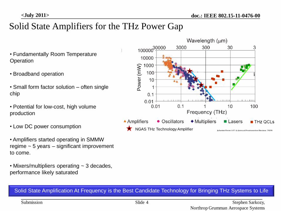
Solid State Amplifiers for the THz Power Gap
Slide 4 Stephen Sarkozy,
Northrop Grumman Aerospace Systems
Po
we
r (m
W)
NGAS THz Technology Amplifier Adapted from UCLA Annual Engineering Review, 2009
Pow
er (m
W)
NGAS THz Technology Amplifier Adapted from UCLA Annual Engineering Review, 2009
Pow
er (m
W)
NGAS THz Technology Amplifier Adapted from UCLA Annual Engineering Review, 2009
Solid State Amplification At Frequency is the Best Candidate Technology for Bringing THz Systems to Life
• Fundamentally Room Temperature
Operation
• Broadband operation
• Small form factor solution – often single
chip
• Potential for low-cost, high volume
production
• Low DC power consumption
• Amplifiers started operating in SMMW
regime ~ 5 years – significant improvement
to come.
• Mixers/multipliers operating ~ 3 decades,
performance likely saturated
<July 2011>
doc.: IEEE 802.15-11-0476-00
Submission Stephen Sarkozy,
Northrop Grumman Aerospace Systems
Slide 5
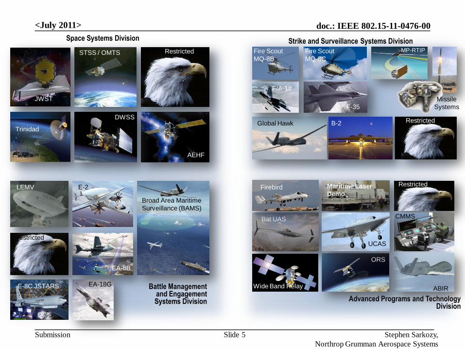
Space Systems Division
Battle Management and Engagement Systems Division Advanced Programs and Technology
Division
EA-18G
EA-6B
Broad Area Maritime
Surveillance (BAMS)
Restricted
LEMV E-2
E-8C JSTARS
Maritime Laser
Demo
Restricted
Bat UAS
ABIRWide Band Relay
ORS
Strike and Surveillance Systems Division
AEHF
STSS / OMTS Restricted
Trinidad
JWST
DWSS
CMMSCMMS
Global Hawk
F-35
Fire Scout
MQ-8B
MP-RTIP
F/A-18
Missile
Systems
B-2 RestrictedGlobal Hawk
Fire Scout
MQ-8C
UCAS
Firebird
<July 2011>
doc.: IEEE 802.15-11-0476-00
Submission
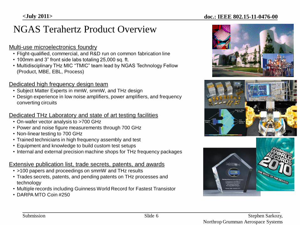
Multi-use microelectronics foundry• Flight-qualified, commercial, and R&D run on common fabrication line
• 100mm and 3” front side labs totaling 25,000 sq. ft.
• Multidisciplinary THz MIC “TMIC” team lead by NGAS Technology Fellow
(Product, MBE, EBL, Process)
Dedicated high frequency design team• Subject Matter Experts in mmW, smmW, and THz design
• Design experience in low noise amplifiers, power amplifiers, and frequency
converting circuits
Dedicated THz Laboratory and state of art testing facilities• On-wafer vector analysis to >700 GHz
• Power and noise figure measurements through 700 GHz
• Non-linear testing to 700 GHz
• Trained technicians in high frequency assembly and test
• Equipment and knowledge to build custom test setups
• Internal and external precision machine shops for THz frequency packages
Extensive publication list, trade secrets, patents, and awards• >100 papers and proceedings on smmW and THz results
• Trades secrets, patents, and pending patents on THz processes and
technology
• Multiple records including Guinness World Record for Fastest Transistor
• DARPA MTO Coin #250
08-02666-024b_02
Complete clean room fabrication facilities with more than 40,000 ft2 of Class 10 clean room space
3 Leica EBL machines for sub 0.1-mm lithography 3 cannon I-line steppers 6 Ultratech g-line steppers Premier producer of advanced HBT and HEMT
integrated circuits for DoD and commercial use Production wafer bonding capabilities
Microelectronics Fabrication Facility
• NGST has complete fabrication facilities (Class 10) ISO 9001 certified
• GaAs production of 20,000 HBT and HEMT wafers per year
• InP production line for high-volume InP
• HBT technology 20,000 ft2
NGST’s Microelectronics Fabrication Facility
• Over 40,000 ft2 of Class 10 clean room space
• Two Leica EBL machines for sub-0.1- m lithography, 1000 wafer/year capacity
• Three cannon I-line steppers
• Six Ultratech g-line steppers
• Premier producer of advanced HBT and HEMT integrated circuits for DoD and commercial use
• Automated CD SEM
Figure A2-1. NGST’s Facilites and Design Capability Complement and Support the Efficient Development of GAN:STAR Technology
• Growth capabilities from 2 inches up to 100 mm
• High volume wafer capabilities• Multiple material suppliers• Material uniformity <2%• Run-to-run reproducibility <3%• Detailed wafer mapping capabilities
NGST’s Microelectronics Epitaxial Capability
• NGST has more than 35 years experience in mixed signal and RF component design
• Mentor Graphics and Cadence design tool for high speed digital design
• Agilent’s Advance Design system for RF MMIC design
• 2D Sonnet and 3D HFSS EM simulation tools for passive component design
NGST’s Component Design Capability
Growth capabilities from 2 inches up to 100 mm High volume wafer capabilities Multiple material suppliers Material uniformity <2% Run-to-run reproducibility <3% Detailed wafer mapping capabilities
Microelectronics Epitaxial Capability
Component Design Capability More than 40 years experience in RF component and mixed signal design
Agilent’s Advanced Design System for RF MMIC design
HFSS, Sonnet and Momentum electromagnetic design tools
Cadence layout tools and dedicated layout support team
ISO 9001 certified Proven III-V production line for 20,000 wafers per
year Trusted foundry Class H and K production
Stephen Sarkozy,
Northrop Grumman Aerospace Systems
Slide 6
NGAS Terahertz Product Overview
<July 2011>
doc.: IEEE 802.15-11-0476-00
Submission
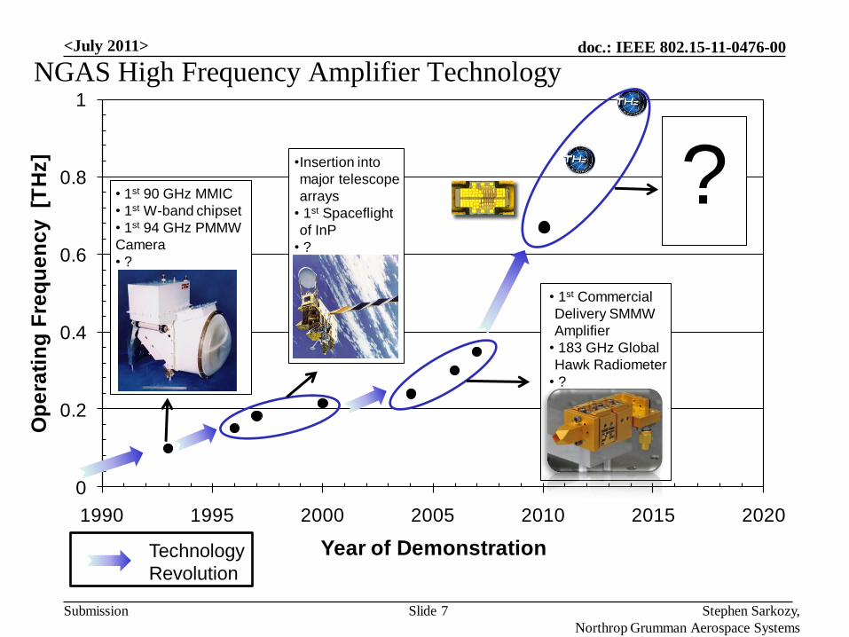
NGAS High Frequency Amplifier Technology
0
0.2
0.4
0.6
0.8
1
1990 1995 2000 2005 2010 2015 2020
Op
era
tin
g F
req
ue
nc
y
[TH
z]
Year of Demonstration
• 1st 90 GHz MMIC
• 1st W-band chipset
• 1st 94 GHz PMMW
Camera
• ?
•Insertion into
major telescope
arrays
• 1st Spaceflight
of InP
• ?
• 1st Commercial
Delivery SMMW
Amplifier
• 183 GHz Global
Hawk Radiometer
• ?
Technology
Revolution
?
Stephen Sarkozy,
Northrop Grumman Aerospace Systems
Slide 7
<July 2011>

doc.: IEEE 802.15-11-0476-00
Submission
Sub-50nm InP HEMT Technology
Frontside
Via Gold
Molecular Beam Epitaxy• 3’’ wafers
• Indium Arsenide Composite Channel (IACC)
• µ > 14000 cm2/V∙s, ns = 3.5 x 1012 cm-2
• Composite cap for tunnel Ohmic Contacts
IACC HEMT IC Features
• Non-alloyed Ohmic Contact
• sub-50nm T-gate
• 600 pF/mm Metal-Insulator-Metal Capacitors
• 20 and 100 Ω/ Thin Film Resistors
• Two layer metal interconnect with air bridges
• PECVD SiN passivation
• Substrate thinning to 25 -75 µm (frequency dependent)
• Scaled transmission lines and passive/active layouts
Process Commonality• Same Fabrication Line for spaceflight, commercial, R&D
• Same MBE, EBL, and process for Low Noise Amplifiers,
Power Amplifiers, and Frequency Conversion circuits
• High Frequency ICs small – multiple designs/circuit on a
single wafer
• Macrocells and System-on-Chip Possibilities
Stephen Sarkozy,
Northrop Grumman Aerospace Systems
Slide 8
<July 2011>
doc.: IEEE 802.15-11-0476-00
Submission
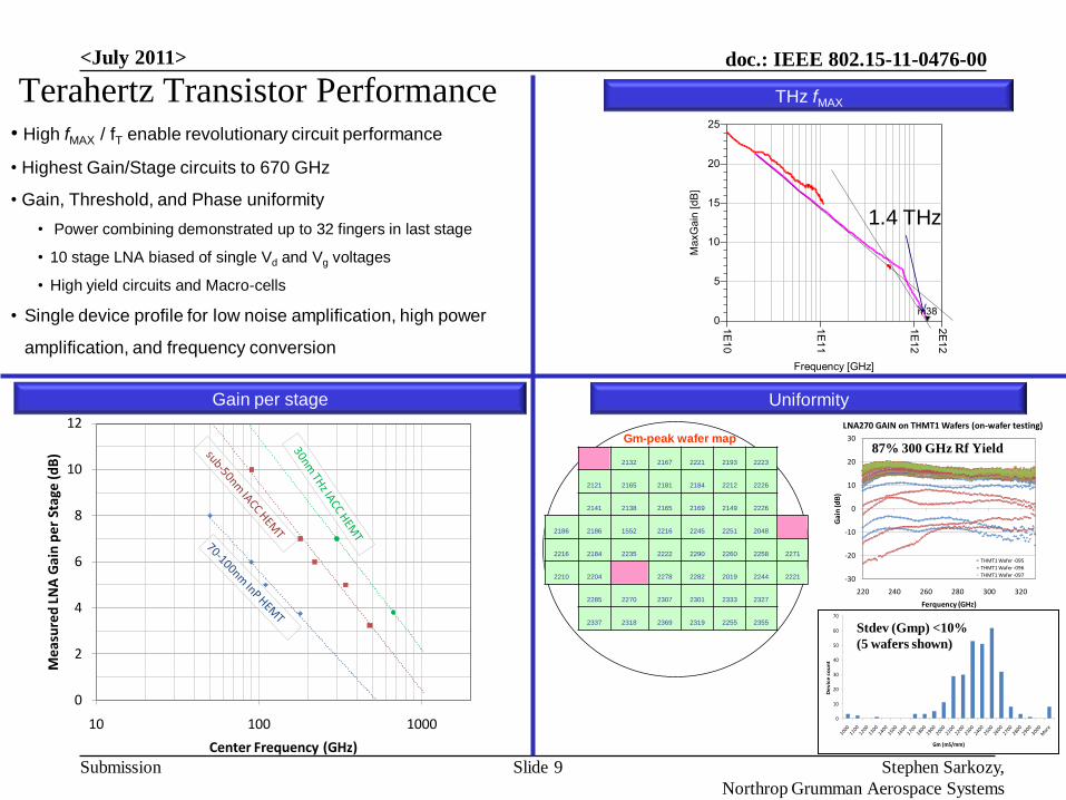
Terahertz Transistor Performance THz fMAX
Gain per stage
• High fMAX / fT enable revolutionary circuit performance
• Highest Gain/Stage circuits to 670 GHz
• Gain, Threshold, and Phase uniformity
• Power combining demonstrated up to 32 fingers in last stage
• 10 stage LNA biased of single Vd and Vg voltages
• High yield circuits and Macro-cells
• Single device profile for low noise amplification, high power
amplification, and frequency conversion
Uniformity
2132 2167 2221 2193 2223
2121 2165 2181 2184 2212 2226
2141 2138 2165 2169 2149 2226
2186 2186 1552 2216 2245 2251 2048
2216 2184 2235 2222 2290 2260 2258 2271
2210 2204 2278 2282 2019 2244 2221
2285 2270 2307 2301 2333 2327
2337 2318 2369 2319 2255 2355
Gm-peak wafer map
0
10
20
30
40
50
60
70
De
vic
e c
ou
nt
Gm (mS/mm)
Stdev (Gmp) <10%
(5 wafers shown)
87% 300 GHz Rf Yield
-30
-20
-10
0
10
20
30
220 240 260 280 300 320
Gai
n (d
B)
Ferquency (GHz)
LNA270 GAIN on THMT1 Wafers (on-wafer testing)
THMT1 Wafer -095
THMT1 Wafer -096
THMT1 Wafer -097
0
2
4
6
8
10
12
10 100 1000
Me
asu
red
LN
A G
ain
pe
r St
age
(d
B)
Center Frequency (GHz)
m38freq=devicemodeling_5_25_2011_THMT2_WR1p5_TL_model..MaxGain1=-0.053
1.400THz
1E
11
1E
12
1E
10
2E
12
5
10
15
20
0
25
Frequency [GHz]
Ma
xG
ain
[d
B]
Readout
m38
m38freq=devicemodeling_5_25_2011_THMT2_WR1p5_TL_model..MaxGain1=-0.053
1.400THz
1.4 THz
Stephen Sarkozy,
Northrop Grumman Aerospace Systems
Slide 9
<July 2011>
doc.: IEEE 802.15-11-0476-00
Submission
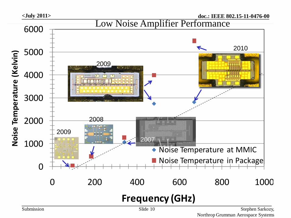
0
1000
2000
3000
4000
5000
6000
0 200 400 600 800 1000
No
ise
Te
mp
era
ture
(K
elv
in)
Frequency (GHz)
Noise Temperature at MMIC
Noise Temperature in Package
2007
11-0
0551_3-0
06
b_
15
4
Frequency [GHz]
Gain
[d
B],
No
ise F
igu
re [d
B]
No
ise T
em
pera
ture
[K]
0
2
4
6
8
10
12
14
16
18
150 160 170 180 190300
400
500
600
700
800
900
1000
1100
1200
Gain [dB]
NF [dB]
NT [K]
Legacy MMIC Noise Figure and Gain
Gain (dB)
RF Frequency (GHz)
Noise Figure (dB)
20
192-200
5.5
Return Losses (dB) 10
GRIFFEN Goals
Legacy MMIC2008
2009
2009
2010
Low Noise Amplifier Performance
Stephen Sarkozy,
Northrop Grumman Aerospace Systems
Slide 10
<July 2011>
doc.: IEEE 802.15-11-0476-00
Submission
-5
0
5
10
15
20
25
30
10 100 1000
Ou
tpu
t P
ow
er (d
Bm
)
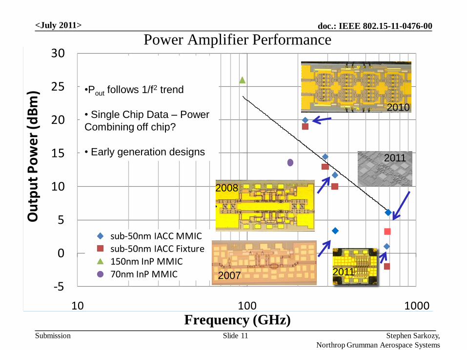
Frequency (GHz)
sub-50nm IACC MMICsub-50nm IACC Fixture150nm InP MMIC70nm InP MMIC 2007
2010
2011
2008
•Pout follows 1/f2 trend
• Single Chip Data – Power
Combining off chip?
• Early generation designs2011
Stephen Sarkozy,
Northrop Grumman Aerospace Systems
Slide 11
Power Amplifier Performance<July 2011>
Frequency (GHz)

doc.: IEEE 802.15-11-0476-00
Submission
Enabling Circuit – 340 GHz LNA
Coplanar Waveguide (CPW)Coplanar Waveguide (CPW)
GNDSignal
InP
GND
-20
-15
-10
-5
0
220 260 300 340
Frequency [GHz]
Retu
rn L
oss [
dB
]
-8
-6
-4
-2
0
Insert
ion
Lo
ss [
dB
]
Sim.
Sim.
Meas.
Meas.
0
-2
-4
-8
-6
0
-5
-10
-20
-15
220 260 340300Frequency (GHz)
Ret
urn
Lo
ss (
dB
)
MeasuredModeled
MeasuredModeled
S21 (d
B)
Stephen Sarkozy,
Northrop Grumman Aerospace Systems
Slide 12
<July 2011>
doc.: IEEE 802.15-11-0476-00
Submission
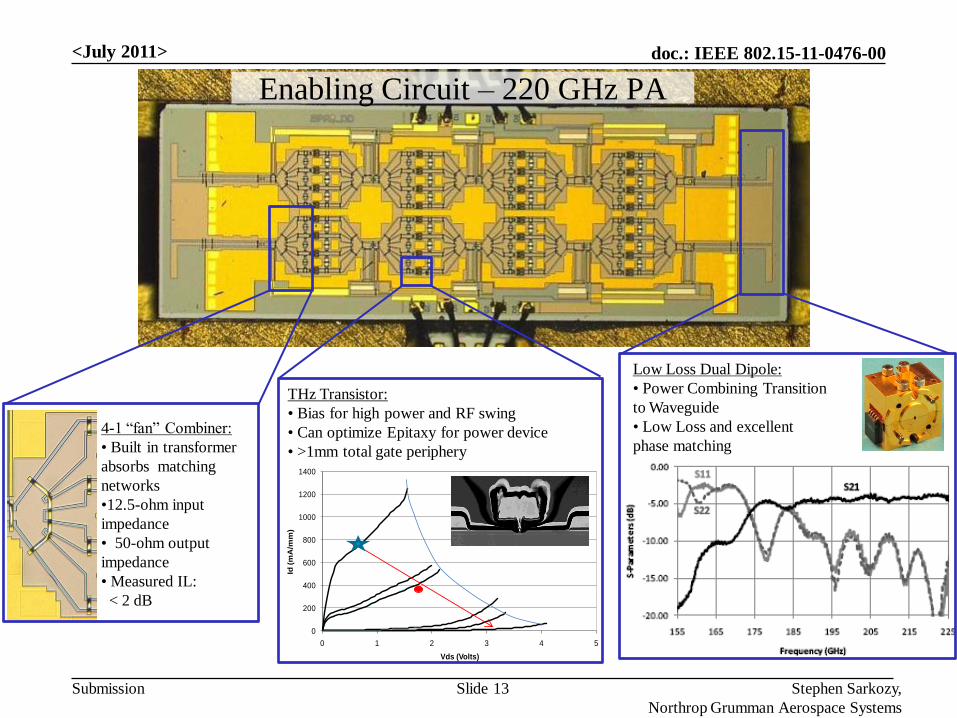
4-1 “fan” Combiner:
• Built in transformer
absorbs matching
networks
•12.5-ohm input
impedance
• 50-ohm output
impedance
• Measured IL:
< 2 dB
Low Loss Dual Dipole:
• Power Combining Transition
to Waveguide
• Low Loss and excellent
phase matching
0
200
400
600
800
1000
1200
1400
0 1 2 3 4 5
Id (
mA
/mm
)
Vds (Volts)
THz Transistor:
• Bias for high power and RF swing
• Can optimize Epitaxy for power device
• >1mm total gate periphery
Stephen Sarkozy,
Northrop Grumman Aerospace Systems
Slide 13
Enabling Circuit – 220 GHz PA
<July 2011>

doc.: IEEE 802.15-11-0476-00
Submission
THz Measurement Capability
THz Metrology Infrastructure “Needs”
• Method for evaluating large sample of designs
• Should be relatively low-cost (not packaged chips)
NGAS THz Metrology Infrastructure Capabilities
• On-Wafer Measurements from 140-950 GHz
• Waveguide Measurements from 70-1000 GHz
• Power Sensors from 70-1000 GHz
• Sources from 180-670 GHz
• Receiver from 180-1000 GHz
THz Collaboration
• Frequency Extenders developed by Virginia Diodes, Inc
• Probes developed by University of Virginia
VNA
Port 1 Extender Port 2 Extender
WR1.5 Probe (UVA)
WR1.5 Probe Station
Probe Configuration
Images of WR-1.5 probe circuits and probe tip
Measurement of 1-mm line with on-wafer TRL Calibration
-180
-120
-60
0
60
120
180
-30
-25
-20
-15
-10
-5
0
500 550 600 650 700 750
Ph
ase [degrees]
S-Pa
ram
eter
s [d
B]
Frequency [GHz]
S21
S11
S21
Stephen Sarkozy,
Northrop Grumman Aerospace Systems
Slide 14
<July 2011>
doc.: IEEE 802.15-11-0476-00
Submission
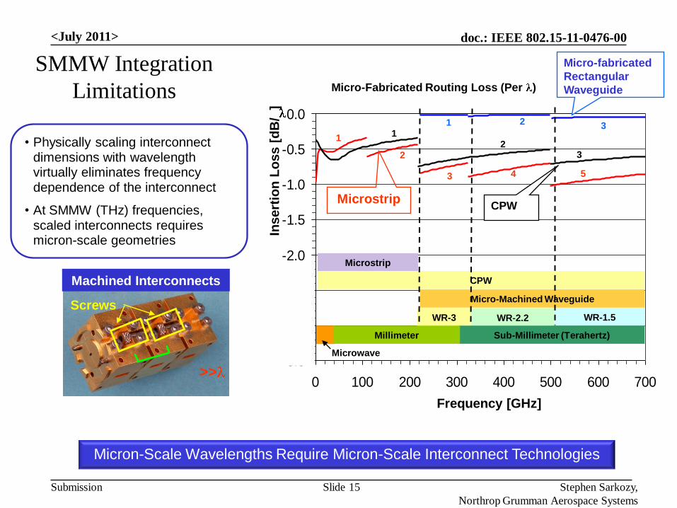
SMMW Integration
Limitations
Micron-Scale Wavelengths Require Micron-Scale Interconnect Technologies
-3.5
-3.0
-2.5
-2.0
-1.5
-1.0
-0.5
0.0
0 100 200 300 400 500 600 700
WR-3 WR-2.2 WR-1.5
Micro-Machined Waveguide
Microstrip
CPW
Sub-Millimeter (Terahertz)Millimeter
Microwave
Micro-Fabricated Routing Loss (Per )
Insert
ion
Lo
ss [
dB
/]
Frequency [GHz]
1
2
3 4 5
12
3
1 2 3
• Physically scaling interconnect dimensions with wavelength virtually eliminates frequency dependence of the interconnect
• At SMMW (THz) frequencies, scaled interconnects requires micron-scale geometries
MicrostripCPW
Micro-fabricated
Rectangular
Waveguide
Machined Interconnects
Screws
>>
Stephen Sarkozy,
Northrop Grumman Aerospace Systems
Slide 15
<July 2011>
doc.: IEEE 802.15-11-0476-00
Submission
WR1.5 Fixture Evolution
• Ripples in transmission measurement, due to
low via density per wavelength, and orthogonal
waveguide modes excited in wide chip fixture
520 540 560 580 600 620 640 660 680500 700
-25
-20
-15
-10
-5
-30
0
Frequency [GHz]
Insert
ion L
oss [
dB
]
WR1.5 Dipole Transition v1
Sim. S21
Meas. S21
375
µm
CPW thru chip in fixture
Chip width
set by circuit
size
Outcome: Need for more densely
spaced vias and reduced chip width
WR2.2 Dipole Transition
475 500 525450 550
-15
-10
-5
-20
0
Frequency [GHz]
Inse
rtio
n L
oss [d
B]
320
µm
CPW thru chip in fixture
• Successful fabrication of 500 GHz
transition on 1-mil InP
Outcome: Demonstration of 1
mil InP chip
Sim. S21 Meas. S21
Test set glitch
-20
-15
-10
-5
0
500 525 550 575 600 625 650 675 700 725 750
Inse
rtio
n Lo
ss [d
B]
Frequency [GHz]
Scaled chip width WR1.5
Transition
270
µm
CPW thru chip in fixture
Outcome: Demonstration of dense
vias, shows need for scaled chip
width, but need more space for
circuit
Sim. S21
Meas. S21
Test set glitch
Stephen Sarkozy,
Northrop Grumman Aerospace Systems
Slide 16
<July 2011>

doc.: IEEE 802.15-11-0476-00
Submission
WR1.5 Fixture Evolution
• Ripples in transmission measurement, due to
low via density per wavelength, and orthogonal
waveguide modes excited in wide chip fixture
520 540 560 580 600 620 640 660 680500 700
-25
-20
-15
-10
-5
-30
0
Frequency [GHz]
Insert
ion L
oss [
dB
]
WR1.5 Dipole Transition v1
Sim. S21
Meas. S21
375
µm
CPW thru chip in fixture
Chip width
set by circuit
size
Outcome: Need for more densely
spaced vias and reduced chip width
WR2.2 Dipole Transition
475 500 525450 550
-15
-10
-5
-20
0
Frequency [GHz]
Inse
rtio
n L
oss [d
B]
320
µm
CPW thru chip in fixture
• Successful fabrication of 500 GHz
transition on 1-mil InP
Outcome: Demonstration of 1
mil InP chip
Sim. S21 Meas. S21
Test set glitch
-20
-15
-10
-5
0
500 525 550 575 600 625 650 675 700 725 750
Inse
rtio
n Lo
ss [d
B]
Frequency [GHz]
Scaled chip width WR1.5
Transition
270
µm
CPW thru chip in fixture
Outcome: Demonstration of dense
vias, shows need for scaled chip
width, but need more space for
circuit
Sim. S21
Meas. S21
Test set glitch
525 550 575 600 625 650 675500 700
-4
-3
-2
-1
-5
0
Frequency [GHz]
Inse
rtio
n L
oss [dB
]
7 mm WR1.5, gold
plated
Loss mechanisms Loss @ 670 GHz
Comments
Transition ~1.7 dB Agrees with simulation, verify CPW loss
515 μm CPW ~2.25 dB Based on W-band data (measure at 670 to verify)
7 mm WG ~0.75 dB Based measuredconductivity at 670 GHz
Total TMIC external loss (WGx2+DPx2)
~4.9 dB Two transitions with waveguide loss
515 μm
Transition
525 550 575 600 625 650 675 700500 725
-35
-30
-25
-20
-15
-10
-5
-40
0
-25
-20
-15
-10
-5
0
5
-30
10
Frequency [GHz]
Insert
ion L
oss [
dB
] Retu
rn L
oss [d
B]
Single Dipole Insertion Loss
De embededmeasurement
Simulation
s11
s22
Sim. Return loss
Sim. Insertion loss
S21
7 mm WR1.5, gold
plated
WR1.5 Integrated dipole probe with thru line
Stephen Sarkozy,
Northrop Grumman Aerospace Systems
Slide 17
<July 2011>
doc.: IEEE 802.15-11-0476-00
Submission
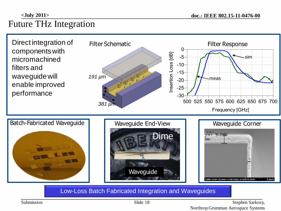
Future THz Integration
Low-Loss Batch Fabricated Integration and Waveguides
Direct integration of
components with micromachinedfilters and
waveguide will enable improved
performance
191 µm
381 µm
Filter Schematic
525 550 575 600 625 650 675500 700
-25
-20
-15
-10
-5
-30
0
Frequency [GHz]
Insert
ion L
oss [dB
]
sim
meas
Filter Response
Batch-Fabricated Waveguide Waveguide End-View
Dime
Waveguide
Waveguide Corner
Stephen Sarkozy,
Northrop Grumman Aerospace Systems
Slide 18
<July 2011>
doc.: IEEE 802.15-11-0476-00
Submission
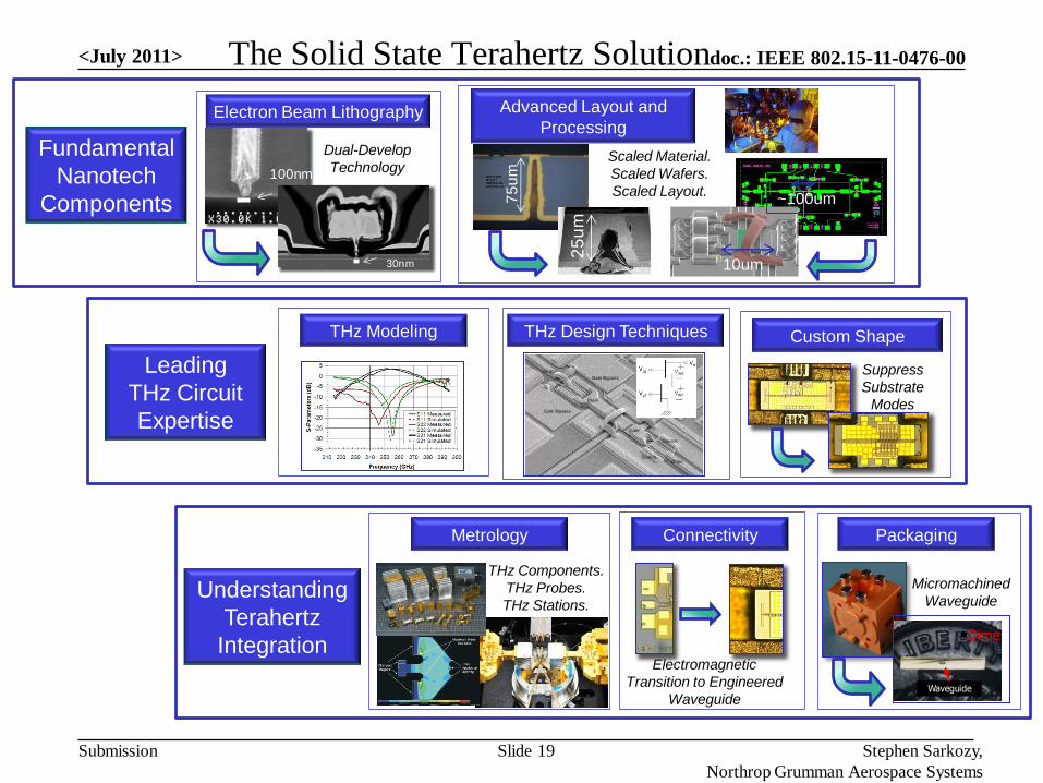
The Solid State Terahertz Solution
Understanding
Terahertz
Integration
Fundamental
Nanotech
Components
Electromagnetic
Transition to Engineered
Waveguide
Connectivity
Dual-Develop
Technology100nm
30nm
Electron Beam Lithography
•Dime
•Waveguide
Micromachined
Waveguide
Packaging
Suppress
Substrate
Modes
Custom Shape
Metrology
THz Components.
THz Probes.
THz Stations.
Leading
THz Circuit
Expertise
THz Modeling THz Design Techniques
Gate Bypass
Gate Bypass
Source
Drain
Gate
DrainSource
Source
75
um
25
um
Scaled Material.
Scaled Wafers.
Scaled Layout.
Advanced Layout and
Processing
~100um
10um
Stephen Sarkozy,
Northrop Grumman Aerospace Systems
Slide 19
<July 2011>

doc.: IEEE 802.15-11-0476-00
Submission
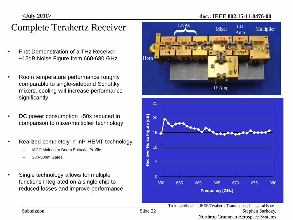
Terahertz Transceiver
LO Amp
LO
IF Amp
•RF
LO Amp
RF out
THz Receiver
LNA
PA
SH Mixer RF in
SH Mixer
THz Transmitter
IF
IF
LNA
PA
670 GHz
LNA TMIC
PA TMIC
LO Amp
IF Amp
SH Mixer
LO Multiplier
LO multiplier
LO multiplier
670 GHz
THz Transceivers are possible with THz amplifiers
•300 GHz LO Port, WR3•670 GHz RF
Input Port, WR1.5
•70 GHz IF Output Port,
WR12
•DC Bias
Stephen Sarkozy,
Northrop Grumman Aerospace Systems
Slide 20
Architecture of DARPA THz Electronics Program
<July 2011>

doc.: IEEE 802.15-11-0476-00
Submission
0
5
10
15
20
25
0
10
20
30
40
50
60
-15 -10 -5 0 5 10 15
Pou
t (dB
m) / G
ain (d
B)
Pou
t (m
W)
Pin (dBm)
BPA3_DP, WR4-e with 5 ohm resistors, fc=217.5 GHz
Pout (mW) Pout (dBm) Gain (dB)
4
5
6
7
8
0
10
20
30
40
50
60
216 217 218 219 220 221 222 223
Ga
in (d
B)
Po
ut,
Pin
(m
W)
Frequency (GHz)
Measured Pout at 217.5 GHz Measured Pout vs. Frequency
Pout (mW)
Gain (dB)
Pin (mW)
Gain (dB)
Pout (mW)
Pout (dBm)
220 GHz PA
• Program Goal - microfabricate vacuum tube
delivering ~5W output power centered at 220 GHz
• 50mW output power at waveguide flange
• Preliminary Life Test - no degradation with > 1
month continual operation at 20mW
0 5 10 15 20 25
0
10
20
30
40
50
60
0 100 200 300 400 500 600 700
50 mW Life-Test Time (Hours)
Po
we
r Ou
t (m
W)
20 mW Life-Test Time (Hours)
Preliminary Life Test
Stephen Sarkozy,
Northrop Grumman Aerospace Systems
Slide 21
Results from DARPA HiFIVE program
<July 2011>
doc.: IEEE 802.15-11-0476-00
Submission
0
5
10
15
20
25
650 655 660 665 670 675 680
Recie
ver
No
ise F
igu
re [
dB
]
Frequency [GHz]
• First Demonstration of a THz Receiver,
~15dB Noise Figure from 660-680 GHz
• Room temperature performance roughly
comparable to single-sideband Schottky
mixers, cooling will increase performance
significantly
• DC power consumption ~50x reduced in
comparison to mixer/multiplier technology
• Realized completely in InP HEMT technology
– IACC Molecular Beam Epitaxial Profile
– Sub-50nm Gates
• Single technology allows for multiple
functions integrated on a single chip to
reduced losses and improve performance
Complete Terahertz Receiver
Horn
{LNAsMixer
LO
AmpMultiplier
IF Amp
Stephen Sarkozy,
Northrop Grumman Aerospace Systems
Slide 22
To be published in IEEE Terahertz Transactions, Inaugural Issue
<July 2011>
doc.: IEEE 802.15-11-0476-00
Submission
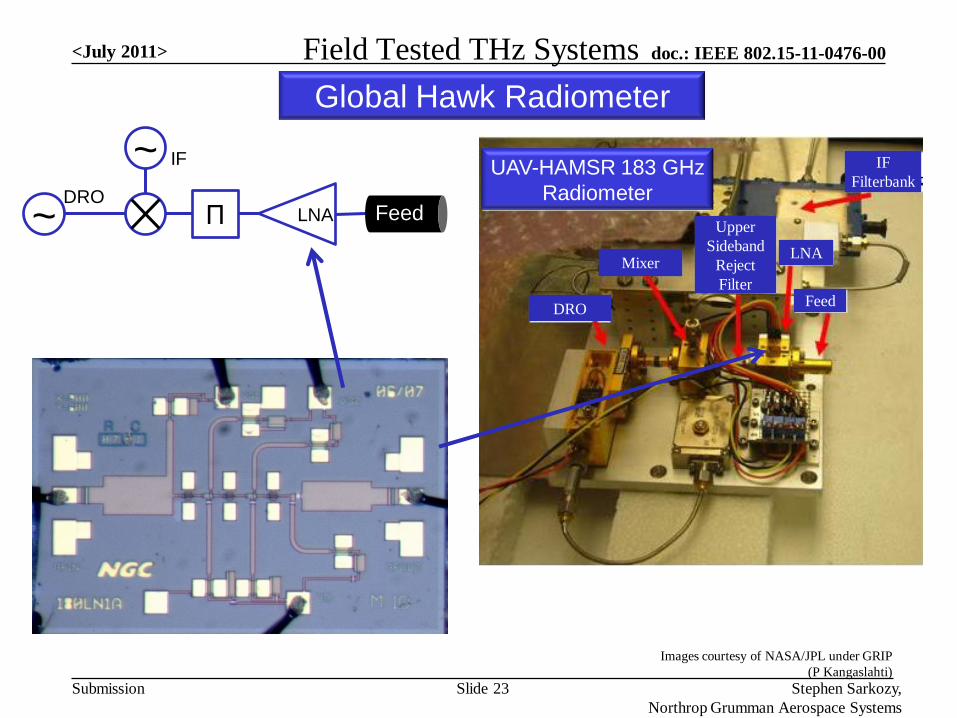
FeedLNA
~ IF
Π~DRO
Field Tested THz Systems
Stephen Sarkozy,
Northrop Grumman Aerospace Systems
Slide 23
Images courtesy of NASA/JPL under GRIP
(P Kangaslahti)
UAV-HAMSR 183 GHz
Radiometer
IF
Filterbank
Feed
LNA
DRO
Mixer
Upper
Sideband
Reject
Filter
Global Hawk Radiometer
<July 2011>

doc.: IEEE 802.15-11-0476-00
Submission
Field Tested THz Systems
Global Hawk Radiometer
Stephen Sarkozy,
Northrop Grumman Aerospace Systems
Slide 24
• 10x improvement in NEΔT
• >150 hours of flight time in
open air housing
• Successful radiometry over
multiple storms including
Hurricane Earl
Images courtesy of NASA/JPL under GRIP
UAV-HAMSR 183 GHz
Radiometer
IF
Filterbank
Feed
LNA
DRO
Mixer
Upper
Sideband
Reject
Filter
<July 2011>
doc.: IEEE 802.15-11-0476-00
Submission
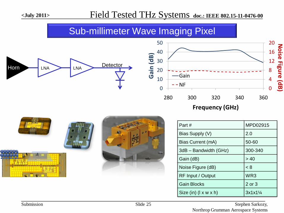
0
4
8
12
16
20
0
10
20
30
40
50
280 300 320 340 360
No
ise Figu
re (d
B)
Gai
n (
dB
)
Frequency (GHz)
Gain
NF
Part # MPD02915
Bias Supply (V) 2.0
Bias Current (mA) 50-60
3dB – Bandwidth (GHz) 300-340
Gain (dB) > 40
Noise Figure (dB) < 8
RF Input / Output WR3
Gain Blocks 2 or 3
Size (in) (l x w x h) 3x1x1¼
LNA LNADetectorHorn
Field Tested THz Systems
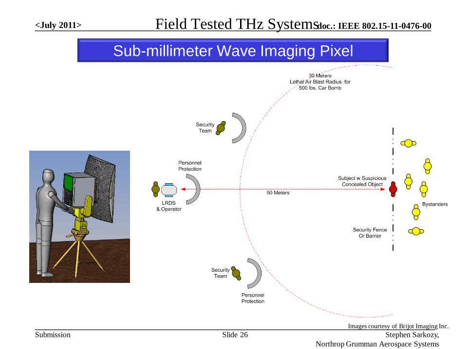
Sub-millimeter Wave Imaging Pixel
Stephen Sarkozy,
Northrop Grumman Aerospace Systems
Slide 25
<July 2011>
doc.: IEEE 802.15-11-0476-00
Submission
Trimmed histogram
Stephen Sarkozy,
Northrop Grumman Aerospace Systems
Slide 26
Images courtesy of Brijot Imaging Inc.
Field Tested THz Systems
Sub-millimeter Wave Imaging Pixel
<July 2011>

doc.: IEEE 802.15-11-0476-00
Submission
Trimmed histogram
Stephen Sarkozy,
Northrop Grumman Aerospace Systems
Slide 27
Images courtesy of Brijot Imaging Inc.
Field Tested THz Systems
Sub-millimeter Wave Imaging Pixel
<July 2011>
doc.: IEEE 802.15-11-0476-00
Submission
Dreams to Solid State RealityMicrointegration and Wafer Level Package for Array Scalability
Aperture Materials Evaluation and Enhancements
-0.35
-0.3
-0.25
-0.2
-0.15
-0.1
-0.05
0
0.05
15 16 17 18 19 20 21 22 23 24 25
Am
plit
ude
[mV
]
Time [nsec]
1.4 nsec
X6 PA X3
Pulsed sourceHorn Antenna
17 GHz 102 GHz 306 GHz
d LO
LNA LNA
X6
10 GHz
24.7 GHz
SHM
IFDetector
Focal Lens
• Quartz
• Kapton
• Mylar
• Metamaterials
• POC Solid State THz Hardware is
performing in the field today, and
demonstrating system value
• Drivers for advancing technology for
immediate future seem to continue to be
military and scientific missions
• Transition to commercial world will
require a paradigm shift
• Compaction
• Cost/Ease of Use
• Propagation Understanding
THz technology pieces exist, is there a player willing to put them together?
Stephen Sarkozy,
Northrop Grumman Aerospace Systems
Slide 28
<July 2011>