Jp Cover Spreads - Yuminaka Lab.133.8.16.23/analog/iedm2005.pdf · of Integrated Silicon...
74
2005 Hilton Washington and Towers Washington, DC December 5-7,2005 Sponsored by Electron Devices Society of IEEE iedm iedm international Electron Devices meeting international Electron Devices meeting
Transcript of Jp Cover Spreads - Yuminaka Lab.133.8.16.23/analog/iedm2005.pdf · of Integrated Silicon...

2005
Hilton Washingtonand TowersWashington, DCDecember 5-7, 2005
Sponsored by Electron Devices Society of IEEE
iedmiedm�
iedmiedm2 0 0 5 C o n f e r e n c ea t a G l a n c e
international Electron Devices meetinginternational Electron Devices meeting
Pres
orted
First
Clas
s Mail
U.S.
Pos
tage
PAID
Rock
ville,
MD
Perm
it No
. 800
1622
0 S.
Fre
deric
k Av
enue
Suite
312
Gaith
ersb
urg,
MD
208
77US
A Adva
nce
Prog
ram
Dec
embe
r 5-
7, 2
005
see
our
hom
e pa
geht
tp://
ww
w.i
eee.
org/
conf
eren
ce/ie
dm
inte
rnat
iona
l Ele
ctro
n D
evic
es m
eetin
gie
dmie
dm20
05
Jp Cover Spreads 10/6/05 12:37 PM Page 1

Date Time International International International Georgetown Jefferson Lincoln Military ThoroughbredBallroom West Ballroom Ballroom East Room Room Room Room Room
CenterSun. 9:00 a.m. -5:30 p.m. Short Course Short Course
Mon. 9:00 a.m. -12:00 p.m. PLENARY
1:30 p.m. - Process Integrated Process Displays, CMOS Solid State CMOS and Modeling and 5:30 p.m. Technology Circuits and Technology Sensors and Devices and Interconnect Simulation
High-k I Manufacturing Advanced MEMS Mobility Nanoelectronic Reliability CompactGate Stacks Advanced Interconnect Organic Enhancement Devices Interconnect, Models
CMOS and Technology and Flexible and Low Non-Volatile Plasma Damage,Platform Electronics Resistance Memory and ESDTechnology Sources/Drain Technologies: Reliability
MONOS and NanocrystalMemories
6:00 p.m. - 7:30 p.m. RECEPTION
Tues. 9:00 a.m. - CMOS Solid State Displays, Integrated Process Quantum Power CMOS and12:00 p.m. Devices and Sensors and Circuits Technology and Compound Interconnect
High Performance Nanoelectronic MEMS and Advanced Semiconductor ReliabilityCMOS Devices MEMS Manufacturing Integration Devices Gate Dielectric
Nanotubes and Technologies DRAM and Concepts High Performance Breakdown —Nanowires for and NAND Si-RF Power and Modeling andThermal and Applications Flash Power-Switching MechanismElectrical DevicesApplications
12:20 p.m. LUNCHEON
2:15 p.m. - Process Emerging Solid State CMOS Modeling and CMOS and Quantum5:30 p.m. Technology Technologies and Devices Simulation Interconnect Power and
High-k II Gate Flexible Nanoelectronic Strained- Nanowires Reliability CompoundDielectrics Electronics Devices Silicon and Process and Semiconductor
Novel Device Technology Nanotubes Electrical DevicesConcepts Degradation in GaN High-PowerFlash Memories Devices, Pushing and Performance the LimitsBoosted CMOS Devices
8:00 p.m. - IEDM Evening IEDM Evening10:00 p.m. Panel Session Panel Session
Wed. 9:00 a.m. - Modeling Process Integrated Circuits CMOS and CMOS Sold State Quantum Power Displays, 12:00 p.m. and Simulation Technology and Interconnect Devices and and Compound Sensors
Transport in Advanced Fully Silicided Gates Manufacturing Reliability SOI and Nanoelectronic Semiconductor and MEMSPlanar CMOS Advanced SRAM Bias-Temperature Multi-Gate Devices Devices Image Sensors and Devices and Novel Integration Instability and Devices Resistive Switching High-Speed Photon Detectors
Technology Interface Traps Memories Compound SemiconductorDevices for Logic &Communications
1:30 p.m. - Process Integrated CMOS Displays, Solid State and Modeling and Quantum Power Modeling and 5:30 p.m. Technology Circuits and Devices Sensors, and Nanoelectronic Simulation and Compound Simulation
Advanced Manufacturing Advanced Gate MEMS Devices Simulation of Semiconductor System Level FEOL Non-Volatile Stacks Thin Film Active and Passive Doping and Devices Device ModelingTechnology Memories Transistors Components in Stress Effects in Silicon Challenges
for Displays and CMOS-Compatible Advanced CMOS Conventional III-VSystem on Panel Technolgies Light Emitters
2 3 4 5 6 7 8 9
10 11 12 13 14 15 16
17 18 19 20 21 22 23
24 25
26 27 28 29 30 31 32 33
34 35 36 37 38 39 40 41
2 0 0 5 C o n f e r e n c e a t a G l a n c eiedmiedm1
Jp Cover Spreads 10/6/05 12:37 PM Page 2

On behalf of the entire IEDM Committee, I would liketo welcome you to the 2005 IEEE InternationalElectron Devices Meeting. We begin our second 50
years of existence honoring the past wealth of technicalwork presented here first as well aslooking forward towards the future ofthis great conference. It continues to bethe premier venue for presenting thelatest, broadest and best technicalinformation of critical importance tosustaining and expanding our worldthrough exciting breakthroughs inelectronic device technologies.
This great tradition continues to growthis year, with what we believe is the bestcollection of contributed and invitedpapers we’ve ever had. They will bepresented by industrial and academicleaders and students from over sixteencountries around the world. Over 670abstracts were submitted this year, a nearrecord, of which more than 240 wereaccepted for presentation at thisconference. Short summaries of eachpaper are included on the IEDM web sitewhich we encourage everyone to visit –http://www.ieee.org/conference/iedm
If you are not already an IEEE member,please consider joining this greatinstitution which has played such animportant role globally for over 120years. More detailed informationregarding IEEE is available at thisconference and on their website –http://www.ieee.org
In addition to the many regular papersessions, we will again feature severalvery special sessions:
On Sunday, two short courses are scheduled entitled: “NextGeneration Semiconductor Manufacturing” and “Low Power‘System-On-Chip’ CMOS Technology Platforms”. They havebeen designed for broad appeal to IEDM participants withmaterial suitable for both newcomers as well as detailed
i e d m 1
JJoonn CCaannddeellaarriiaaGeneral Chair
KKaaiizzaadd MMiissttrryyTechnical Program
Chair
HH..SS.. PPhhiilliipp WWoonnggTechnical Program
Vice Chair
C O N F E R E N C EW E L C O M E F R O M T H E
G E N E R A L C H A I R
Jp pg1-13 10/5/05 9:00 AM Page 1
enough for experts in their fields. These courses have beenorganized and will be presented by internationally-knownleading researchers active in their respective areas oftechnology.
The Plenary Session on Monday morning will feature thefollowing invited talks – “More Than Moore:Micromachined Products Enable New Applications andOpen New Markets”, presented by Benedetto Vigna from STMicroelectronics; “Scaling, Power and the Future of CMOS”,given by Mark Horowitz, Stanford University and Rambus,Inc.; and “Past and Future of Information Displays”, byKouji Suzuki, Toshiba Corp. and SED, Inc.
The Emerging Technology special session this year featuresbreakthroughs in the area of Flexible Electronics, and willinclude five talks from leading experts in this exciting newarea looking from a broad variety of perspectives includingmaterials, processing and structures, as well as systems andapplications.
On Tuesday night, we will again feature our popular andinteractive Panel sessions. This year we will explore thequestions “Will Non-Volatile Memory Technology Scale Pastthe End of the Decade?” and “Semiconductor Research andDevelopment: Who Will Do It and Who Will Pay For It In2010?” These discussions will be lead by two great sets ofinternationally-known panelists and moderators.
And last but certainly not least, on behalf of the IEEEElectron Device Society which sponsors IEDM, KaizadMistry, Technical Program Chair, and Philip Wong,Technical Program Vice-Chair, I want to express our sincereappreciation to each of the members of the IEDMcommittee for the outstanding job they have done inplanning and organizing the 2005 conference. Likewise, allof the authors are to be commended for their tremendousefforts in preparing and sharing their latest work with us,covering so many fields of great importance and interest toour global technical audience.
It is again my great honor and pleasure to extend a warmwelcome to everyone attending the 2005 IEEE InternationalElectron Devices Meeting.
Jon CandelariaGeneral Chair
2 i e d m
Jp pg1-13 10/5/05 9:00 AM Page 2

C O N F E R E N C E
S H O R T C O U R S E SSunday, December 4, 9:00 a.m. - 5:30 p.m.
International Ballroom East, International Ballroom Center
P L E N A R Y S E S S I O N
Monday, December 5, 9:00 a.m. - 12:00 p.m.International Ballroom Center
P L E N A R Y S E S S I O N AWA R DP R E S E N T A T I O N S
2004 Roger A. Haken Best Student Paper Award:To: Masumi Saitoh, University of TokyoFor the paper entitled: “Room Temperature Demonstrationof Integrated Silicon Single-electron Transistor Circuits forCurrent Switching and Analog Pattern Matching”
2005 EDS Chapter of the Year AwardTo: To Be Announced
“To an EDS chapter, based on the quantity and quality of theactivities and programs implemented by the chapter.”
2005 EDS Graduate Student Fellowship AwardTo: Christopher Morris, University of Washington; ElenaSmotrova, National Academy of Sciences of Ukraine; Sun-Jung Kim, The National University of Singapore; and TonyAik Seng Low, The National University of Singapore “
“To promote, recognize, and support graduate level studyand research within the Electron Devices Society’s field ofinterest.”
2005 George E. Smith AwardTo: Zhi-Yuan Charles Cheng, Arthur J. Pitera, Minjoo LarryLee, Jongwan Jung, Judy L. Hoyt, Dimitri A. Antoniadis, andEugene A. Fitzgerald
For the paper entitled: “Fully Depleted Strained-SOI n- andp-MOSFETs on Bonded SGOI Substrates and Study of theSiGe/BOX Interface”
2005 Paul Rappaport AwardTo: Franco Stellari, Peilin Song, James C. Tsang, Moyra K.McManus and Mark B. Ketchen
For the paper entitled: “Testing and Diagnostics of CMOSCircuits Using Light Emission from Off-State LeakageCurrent”
C O N F E R E N C E H I G H L I G H T S
i e d m 3
Jp pg1-13 10/5/05 9:00 AM Page 3

C O N F E R E N C E H I G H L I G H T S
2005 IEEE/EDS Fellows(Only includes those who requested to be
recognized at the IEDM)
Supriyo Bandyopadhyay, Virginia CommonwealthUniversity, Richmond, VA, USA
”For contributions to device applications of nanostructures.”
Duane S. Boning, Massachusetts Institute of Technology,Cambridge, MA, USA
”For contributions to modeling and control insemiconductor manufacturing.”
Jeff D. Bude, Agere Systems, New Providence, NJ, USA
”For contributions to the deep submicron MOSFETs.”
Robert S. Chau, Intel Corporation, Beaverton, OR, USA
”For contributions to gate dielectric and transistortechnology for microprocessors.”
Guido V. Groeseneken, IMEC, Leuven, Belgium
”For his contributions to the physical understanding and themodeling of reliability of metal oxide semiconductor fieldeffect transistors.”
James Albert Hutchby, Semiconductor Research Corp.,Research Triangle Park, NC, USA
”For leadership in the development of high-efficiency solarcells and heterojunction bipolar transistors.”
Masaaki Kuzuhara, University of Fukui, Japan“For contributions to group III-V microwave devices.”
John Melngailis, University of Maryland, College Park, MD,USA
”For contributions to focused ion beam applications.”
Mehrdad J. Moslehi, Semizone Inc., Palo Alto, CA, USA
”For contributions to single wafer processing technologies.”
Laurence W. Nagel, Omega Enterprises, Randolph, NJ, USA
”For contributions to the field of integrated circuitsimulation.”
4 i e d m
Jp pg1-13 10/5/05 9:00 AM Page 4

C O N F E R E N C E H I G H L I G H T S
Hidehito Obayashi, Hitachi High-Technologies Corporation,Hitachinaka, Ibaraki, Japan
”For contributions to critical dimension scanning electronmicroscopy.”
Yutaka Ohmori, Osaka University, Suita, Osaka, Japan
”For contributions to the development of organic andsemiconductor light emitting materials and devices.”
Enrico Sangiorgi, University of Bologna, Cesna, FC, Italy
”For contributions to the modeling and characterization ofhot carriers and non stationary transport effects in smallsilicon devices.”
Tangali S. Sudarshan, University of South Carolina,Columbia, SC, USA
”For contributions to surface flashover of dielectric andsemiconductor materials.”
Juzer M. Vasi, Indian Institute of Technology (IIT), Bombay,Mumbai Maharashtra, India
”For leadership in microelectronics education.”
Sophie V. Verdonckt-Vandebroek, Xerox Corporation,Webster, NY, USA
”For leadership in developing document systems.”
Donald Coolidge Wunsch, University of Missouri - Rolla,Rolla, MO, USA
”For contributions to hardware implementations ofreinforcement and unsupervised learning.”
2005 EDS Distinguished Service AwardTo: Cary Y. Yang
“To recognize and honor outstanding service to the ElectronDevices Society.”
2005 J.J. Ebers AwardTo: To Be Announced
“To honor a single or a series of contributions of recognizedscientific, economic, or social significance in the broad fieldof electron devices”
i e d m 5
Jp pg1-13 10/5/05 9:00 AM Page 5
C O N F E R E N C E H I G H L I G H T S
6 i e d m
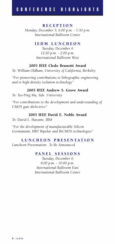
R E C E P T I O NMonday, December 5, 6:00 p.m. - 7:30 p.m.
International Ballroom Center
I E D M L U N C H E O NTuesday, December 6
12:20 p.m. - 2:00 p.m.International Ballroom West
2005 IEEE Cledo Brunetti AwardTo: William Oldham, University of California, Berkeley
“For pioneering contributions to lithographic engineeringand to high-density isolation technology”
2005 IEEE Andrew S. Grove AwardTo: Tso-Ping Ma, Yale University
“For contributions to the development and understanding ofCMOS gate dielectrics”
2005 IEEE David E. Noble AwardTo: David L. Harame, IBM
“For the development of manufacturable SiliconGermanuim, HBT Bipolar and BiCMOS technologies”
L U N C H E O N P R E S E N T A T I O NLuncheon Presentation: To Be Announced
P A N E L S E S S I O N STuesday, December 6
8:00 p.m. - 10:00 p.m.International Ballroom East
International Ballroom Center
Jp pg1-13 10/5/05 9:00 AM Page 6

G E N E R A L I N F O R M A T I O N
i e d m 7
international Electron Devices meeting
iedmiedm2005
G E N E R A L I N F O R M A T I O NHilton Washington
1919 Connecticut Avenue, NWWashington, DC 20009
202-483-3000December 5-7, 2005
R E G I S T R A T I O NI N F O R M A T I O N
Advance After(Postmarked by November 11th orNovember 11th) at Conference
Technical SessionIEEE Member $395.00 $435.00Non-member $485.00 $525.00Students:
Member $ 50.00 $ 50.00Non-Member $ 85.00 $ 85.00
Short Courses Member $400.00Non-member $450.00Student $100.00
Short Courses (Due to limited space, it is recommended thatyou register in advance for the Short Courses)
Payment of the Technical Session registration fee entitles theregistrant to one copy of the Technical Digest, one CD-ROM,one ticket for the Monday evening Wine and CheeseReception and entrance to all technical sessions. TechnicalSession registration does not include entrance to the ShortCourses. TO QUALIFY FOR THE MEMBERREGISTRATION FEE, REGISTRANT MUST BE A MEMBEROF IEEE PRIOR TO THE CONFERENCE.Payment of the Short Course registration fee entitles theregistrant to entrance to one short course, one copy of thecourse workbook and one copy of the CD-ROM of the shortcourse workbook. Short Course registration does notinclude entrance to the Technical Sessions.
Jp pg1-13 10/5/05 9:00 AM Page 7

For Advance Registration, complete the AdvanceRegistration Card (see centerfold) and return withremittance of appropriate registration fee NO LATER THANNOVEMBER 11, 2005 to qualify for the early registrationprice. Due to limited space, it is recommended that youregister in advance to attend the Short Courses.
Confirmations will be sent out to all conference registrants.
REGISTRATION FORM AND PAYMENT SHOULD BESENT TO:
IEDM16220 S. Frederick AvenueSuite 312Gaithersburg, MD 20877 USA301-527-0900, ext 103
Checks MUST BE MADE PAYABLE TO IEDM, IN U.S.DOLLARS AND DRAWN ON A U.S. BANK. Internationalregistrants should not send wire transfers. If Internationalparticipants cannot send a check prior to the conference,mail the registration form without payment prior to theconference. Bring payment with you and pay theregistration fee onsite.
Your registration materials will be held for you at theconference. Your cancelled check is your receipt.
CANCELLATION POLICY: You are encouraged to registerin advance for your own convenience. Due to printing andhotel commitments, refunds requested after November 11cannot be guaranteed. A $30.00 processing fee will bewithheld from ALL refunds.
REGISTRATION CENTER: The Conference RegistrationCenter, located in the Lower Concourse of the HiltonWashington, will be open as follows:
SHORT COURSE REGISTRANTS ONLY
Saturday, December 3 5:00 p.m.- 7:00 p.m.Sunday, December 4 8:00 a.m.- 12:00 p.m.
TECHNICAL SESSION REGISTRANTS
Sunday, December 4 2:00 p.m. - 5:00 p.m.Monday, December 5 8:00 a.m. - 5:00 p.m.Tuesday, December 6 8:30 a.m. - 5:00 p.m.Wednesday, December 7 8:30 a.m. - 3:00 p.m.
I N F O R M A T I O NG E N E R A L I N F O R M A T I O N
8 i e d m
Jp pg1-13 10/5/05 9:00 AM Page 8

G E N E R A L
HOTEL RESERVATIONS: A block of rooms at the HiltonWashington has been reserved for IEDM participants.Special IEDM room rates are as follows:
Single/Double: $186/$208Plus a 14.05% city tax.
To make a reservation, please complete the HotelReservation Form (see centerfold) and return directly to theHilton Washington NO LATER THAN NOVEMBER 10th toqualify for a room under our special rates. An advancedeposit or credit card guarantee is necessary to hold yourroom, if arrival is scheduled after 6:00 p.m.
SHORT COURSES: The IEDM sponsors two short courseson Sunday, December 4, from 9 a.m. to 5:30 p.m. Thecourses are “Low Power ‘System On Chip’ CMOSTechnology Platforms and “Next Generation SemiconductorManufacturing” These courses will be presented by expertsin the fields. Lectures will start with introductory materialfor the general audience and progress towards description ofthe latest developments.
To register, complete the Advance Registration form (seecenterfold). The registration fee is $400 for members and$450 for non-members and includes a visuals booklet, CD-ROM, refreshments and lunch. Attendance is limited, soadvanced registration is recommended.
EVENING PANEL DISCUSSIONS: On Tuesday evening,December 6, beginning at 8:00 p.m., the IEDM will offertwo evening Panel Discussions on timely issues.
1. Will Non-Volatile Memory Technology Scale Past the Endof the Decade?2. Semiconductor Research and Development: Who Will DoIt and Who Will Pay For It In 2010?
SPEAKER PREPARATION ROOM: The IEDM will sponsora Speaker Preparation Room for speakers to preview theirpresentations. Speakers must preview their presentations 1day in advance. There will be no previewing ofpresentations the day of the presentation.
The Speaker Ready Room will be open for speaker use:Saturday, December 3 5:00 p.m. – 7:00 p.m.Sunday, December 4 8:00 a.m. – 5:00 p.m.Monday, December 5 8:00 a.m. – 5:00 p.m.Tuesday, December 6 8:00 a.m. – 5:00 p.m.Wednesday, December 7 8:00 a.m. – 12:00 p.m.
G E N E R A L I N F O R M A T I O N
i e d m 9
Jp pg1-13 10/5/05 9:00 AM Page 9
I N F O R M A T I O N
IEDM LUNCHEON: The IEDM luncheon will be held onTuesday, December 6, at 12:20 p.m. in the InternationalBallroom West. Luncheon tickets are available throughAdvance Registration or on-site at a cost of $45.00 toconference attendees only.
WINE AND CHEESE RECEPTION: A Wine and CheeseReception for conference participants and their guests willbe held on Monday, December 5 from 6:00 p.m. to 7:30p.m. in the International Ballroom. ONE ADMISSION TOTHE RECEPTION IS INCLUDED IN THE REGISTRATIONFEE.
TECHNICAL DIGEST and CD-ROM: Extra copies of theTechnical Digest/CD-ROM can be purchased by conferenceregistrants through Advance Registration. A LIMITEDnumber of Digests will be for sale after 2:00 p.m. onTuesday, December 6 at the On-Site Registration Desk of theConference. The unit cost of the Digest, if ordered throughAdvance Registration or purchased on-site is $125.00.Digests will be available after the conference by mail fromIEEE Service Center, 445 Hoes Lane, Piscataway, NJ 08855.Customer Service Department 732-981-0060 or toll free:800-678-4333, email is [email protected]. ONECOPY OF THE TECHNICAL DIGEST/CD-ROM ISINCLUDED IN THE REGISTRATION FEE.
MEMBERSHIP PROMOTION FOR NON-IEEE MEMBERS:Conference registrants will be able to join IEEE, and theElectron Devices Society (EDS) during the conference at theIEEE Membership Desk located in the Registration Center.If you registered and paid for the conference as a non-member, you will be receiving a CREDIT voucher worth$25 towards an IEEE membership, and free EDSmembership for one year (worth $11). STUDENTSregistering at the student, non-member rate will receive acredit voucher that will entitle them to one-year of FREEIEEE and EDS memberships.
MEMBERSHIP PROMOTION FOR CURRENT IEEEMEMBERS: FREE Electron Devices Society membershipfor one-year will be offered to any IEEE memberattending the IEDM who is not currently a member ofEDS. A FREE EDS Membership Credit Voucher will beavailable at the IEEE Membership Desk. Just complete thevoucher by providing your name, address and membernumber and submit it at the Membership Desk. If you arecurrently a member of EDS, you cannot use this voucher torenew your membership. Credit vouchers are only valid atthe IEDM and must be redeemed at the IEEE MembershipDesk. Copies of the 2006 EDS Membership Brochure are
G E N E R A L I N F O R M A T I O N
1 0 i e d m
Jp pg1-13 10/5/05 9:00 AM Page 10
G E N E R A L
also available at the Membership Desk, which will be openthe following hours:
Monday, December 5 9:00 a.m. - 5:00 p.m.Tuesday, December 6 9:00 a.m. - 5:00 p.m.Wednesday, December 7 9:00 a.m. - 3:00 p.m.
MESSAGE CENTER: An IEDM Message Board will be inoperation in the Registration Center during registrationhours. Please advise callers who wish to reach you duringthe day to ask the hotel operator 202-483-3000 for theIEDM Conference Message Desk. Please check the messageboard periodically.
ROGER A. HAKEN BEST STUDENT PAPER: The 2004Roger A. Haken Best Student Paper will be presented onMonday, December 5, at the Plenary Session to MasumiSaitoh, University of Tokyo for the paper entitled, “RoomTemperature Demonstration of Integrated Silicon Single-Electron Transistor Circuits for Current Switching andAnalog Pattern Matching.”
One paper presented by a student at the 2005 IEDM will beselected for the 2005 Best Student Paper Award. To beeligible, the paper must be based on the student’s own workand have been identified as a student paper at the time ofsubmission. Presentation of the award will be made at the2006 IEDM.
BADGES: Badges are required for admittance to all sessionsand the Wine and Cheese Reception. Please wear yourbadge at all times while attending the conference, so thatyou will not be delayed entry to a session.
PRESS ROOM: Beginning on Monday, the Press Room, willbe in operation during registration hours.
AIRPORT TRANSPORTATION: The Washington FlyerShuttle Bus and taxi service is available from the RonaldReagon National Airport and Dulles Int’l to the HiltonWashington. The following estimated rates are subject tochange:Washington Flyer Suttle Bus - $20 one way/ $30 round TripTaxi - $50 one way
RECRUITING: In keeping with the long standing traditionof fostering a low key, research oriented atmosphere for theIEDM, the Conference Committee and the Electron DevicesSociety of the IEEE discourage overt and highly visiblerecruiting activities in association with the IEDM. IEEE
G E N E R A L I N F O R M A T I O N
i e d m 1 1
Jp pg1-13 10/5/05 9:00 AM Page 11
I N F O R M A T I O N
policy #9.l8 prohibits recruiting at IEEE-sponsoredconferences, consequently, recruiters and recruitmentadvertisements will not be permitted in IEDM hotel space ormeeting facilities and all unauthorized material will beremoved from the premises.
PLEASE DIRECT CONFERENCE INQUIRIES TO:Phyllis Mahoney
2005 IEDM16220 S. Frederick Road, Suite 312
Gaithersburg, MD 20877 USATEL: 301/527-0900 EXT. 103
FAX: 301/527-0994EMAIL: [email protected]
G E N E R A L I N F O R M A T I O N
1 2 i e d m
Jp pg1-13 10/5/05 9:00 AM Page 12

Seated from left to right: Paolo Pavan, EuropeonArrangements Co-Chair, Ralf Brederlow, Short Course Chair,Vivek Subramanian, Publicity Vice Chair, Kaizad Mistry,Technical Program Chair, Jon Candelaria, General Chair, H.-S. Philip Wong, Technical Program Vice Chair, ThomasBonifield, Publicity Chair, Thomas Skotnicki, EuropeanArrangements Co-Chair
Standing from left to right: Phyllis Mahoney, ConferencePlanner, Akintunde Akinwande, Diplays, Sensors and MEMSChair, Carlos Diaz, Asian Arrangements Co-Chair, ConorRafferty, Modeling and Simulation Chair, Toshiro Hiramoto,CMOS Devices Chair, Chris Auth, Short Course Vice Chair,Ashraf Alam, CMOS and Interconnect Reliability Chair,Kazunari Ishimaru, Asian Arrangements Co-Chair, GlenWilk, Process Technology Chair, Gaudenzio Meneghesso,Quantum Power and Compound Semiconductor DevicesChair, Bruce White, Solid State and Nanoelectronic DevicesChair, Meikei Ieong, Publications Chair, Luan Tran,Integrated Circuits and Manufacturing Chair, MelissaWiderkehr, Conference Planner
Missing: Veena Misra, Emerging Technologies Chair
2 0 0 5 I E D M C O N F E R E N C E A N DP R O G R A M C O M M I T T E E
i e d m 1 3
Jp pg1-13 10/5/05 9:00 AM Page 13

S U N D A Y
1 4 i e d m
SHORT COURSE:Low Power “System On Chip” CMOS Technology Platforms
Sunday, December 4, 9:00 a.m. – 5:30 p.m.International Ballroom CenterCourse Organizers: Margaret Huang, Freescale Semiconductor
Suresh Venkatesan, Freescale SemiconductorLow Power technologies serve the rapidly growing portableelectronics market including laptop computers, PDAs, cell phones,WLAN/WPAN connectivity devices, MP3 players, etc. A wide rangeof semiconductor technologies and design techniques serve thismarket. This short course will focus on CMOS SoC technologyplatform technologies and design techniques essential for enablingthis market segment.
The short course is organized to focus on three areas: technology,design and modeling. The first lecture will discuss therequirements and transistor design issues in current and future lowpower technologies. The course will focus on issues and tradeoffsbetween low standby and low active power device design and willconclude with requirements for future innovations in low powerprocess and transistor design. The second lecture will discussembedded memory technologies critical for low power systems.Challenges and technology requirements as well as trends inembedded SRAM, DRAM, NV memory and emerging memorytechnologies will be discussed. The third and fourth lecture willcover digital and analog/RF circuit design aspects with specialemphasis on technology and circuit co-optimization for low powersystems using nanometer CMOS technologies. The digital designsection will discuss general challenges for low power technology,discuss in detail circuits for leakage avoidance, control andtolerance, low power architectures and various system powermanagement concern and conclude with discussion on technology,circuits, architecture and system co-optimization. The lecture onanalog/RF designs will cover the impact of scaled CMOS on keydesign Figures-of-Merit, followed by discussion on specificanalog/RF design blocks and the challenges for technology anddesign co-optimization for designs such as Op-Amps, converters,LNAs and VCOs. The final lecture will focus on modeling of scaledCMOS with emphasis on the modeling aspects critical for lowpower systems. Reduced supply voltages and the push to operate atlow currents mean that the accuracy of near- and below-thresholdmodeling for MOSFETs is of prime importance, yet this is preciselywhere many existing models have the least physical accuracy.Modern surface-potential based models are recognized as the mostphysical and accurate near threshold, and will be reviewed in detail.Other critical near threshold modeling aspects including variability,noise and leakage current will also be discussed. Through thisseries of lectures, a comprehensive overview of state of the art LowPower SoC CMOS platforms will be provided.
Jp 14-62 10/10/05 11:05 AM Page 14

S U N D A Y
i e d m 1 5
Process TechnologyInstructor: Scott Crowder, IBM
What is a Low Power Process?Low Standby vs. Low Active PowerLow Cost vs. High Performance
Transistor Design for Low Standby PowerStandby Power Components
Scaling ChallengesMethods for Parasitic Leakage ReductionMaterials/Innovations for Performance Scaling
Transistor Design for Low Operating PowerOperating Power Components
Scaling ChallengesMobility EngineeringMaterials/Innovations for Performance Scaling
Additional Requirements for Low Power “System On Chip”Technology
BEOL ScalingPassive Elements
Embedded Memory Technology for Low PowerSystems
Instructor: Yasushi Yamagata, NEC Electronics
Importance of Embedded MemoryMemory Content TrendSingle-Core to Multi-Core
SRAM Challenges with Device ScalingLow Voltage OperationDevice VariabilityLeakagesSERSolution Candidate
Embedded DRAMAdvantage/Requirement of Embedded DRAMTechnology TrendTrench vs.Stack
Embedded DRAM ApplicationEmbedded NV Memory
Advantage/Requirement of Embedded NVTechnology Trend Floating Gate vs. Charge TrapEmbedded Flash for ROM Replacement
Emerging Memory TechnologyOverview of Various Technologies – Performance Trade-offsMRAM Technology - Issues and Future ProspectsNano-Bridges
Digital Design for Low Power SystemsInstructor: Shekhar Borkar, Intel
Active and Leakage Power Challenges Technology OutlookActive and Leakage Power Projections Cost
Circuits for Leakage Avoidance, Control, and Tolerance Dual Vt, Body Bias, Stack Effect, and Sleep TransistorTechniques Leakage Tolerant High Performance Circuits Leakage Control for Memory Circuits
Jp 14-62 10/10/05 11:05 AM Page 15

S U N D A Y
1 6 i e d m
Microarchitectures for Low Power Optimum Logic Pipelines Throughput Oriented Designs Multi-Everywhere: From Threads To Cores Technology and Design Co-Optimization Challenges
System Power Management Fine Grain Power Management Power Delivery Low Power Platform Design Power Management Software
Technology, Circuits, Microarchitecture, and System Co-Optimization
Analog/RF Design in Nanometer CMOSTechnologies
Instructor: Willy Sansen, KU Leuven
Impact of Nanometer Channel Lengths on Transistor PerformanceIntrinsic Gain ReductionSpeed EnhancementNoise - Thermal and 1/f NoiseOffset Distortion Cancellation
Operational Amplifiers with Supply Voltage Below 1 V and withMinimum Power Consumption
Gate-Driven, Bulk-Driven Single-Stage AmplifiersTwo-Stage Miller Op-Amps Multi-Stage AmplifiersTechnology and Design Co-Optimization Challenges
Low-Voltage Low-Power Delta-Sigma A-to-D ConvertersSwitched Op-Amp ApproachFull-Feedforward ApproachInput-Series-Resistor ApproachTechnology and Design Co-Optimization Challenges
Communication CircuitsVCO’s with Low Phase NoiseLNA’s with Low Noise FigureTechnology and Design Co-Optimization Challenges
Modeling for Digital and AMS/RF DesignInstructor: Colin McAndrew, Freescale Semiconductor
OverviewModeling Challenges and needs for Low-PowerAdditional Challenges from Technology ScalingDigital and Analog NeedsLinkage to Circuit and System Level Design and Simulation
MOSFET ModelingAccurate Near-Threshold Modeling, State-of-the-Art SurfacePotential ModelsVariability Exacerbation from Technology Scaling and LowPower OperationNoiseProximity Effects
Passive and Parasitic ModelingShift in the Nature of Parasitic Capacitances, Dependence onAdjacent StructuresDifficulties in Modeling of and Importance of Leakage for StaticPower
Jp 14-62 10/10/05 11:05 AM Page 16

S U N D A Y
i e d m 1 7
System Level ModelingSystem and Architecture Level Modeling and Optimization forLow Power DesignDynamic and Static Power Dissipation
SHORT COURSE:Next Generation Semiconductor Manufacturing
Sunday, December 4, 9:00 a.m. - 5:30 p.m.International Ballroom EastCourse Organizer: C. Rinn Cleavelin, Texas InstrumentsThe last 2-3 generations of semiconductor manufacturing havepresented some unique challenges. As the traditional scaling lawshave started to slow, new materials have been increasingly added inorder to continue the consistent gains in performance. These newmaterials have placed new requirements beyond just the typicalscaling of feature sizes. Additionally the varieties of end-userrequirements for ICs have led to a proliferation of processes tailoredto the features of the application. These shifts have led to a need forsubstantial innovation in order to enable manufacturing of multi-core, multi-GHz microprocessors, multi-Gb memories, and lowpower SoCs. Frequently in the same factory! This short course willexamine the requirements for the processes, from FEOL and BEOLto packaging to yield and reliability, that will be needed in order toproduce these chips at high performance, high density and lowcost. Through the five lectures, the speakers will detail the state ofthe art in process technology, the trends in development andprovide insight into what the next generation of semiconductormanufacturing will look like.
The first lecture consists of an overview of the state ofsemiconductor manufacturing and what the future holds. Thisincludes the global business trends, the impacts of introducing newmaterials and novel device architectures, and the outlook for450mm wafers. The second lecture focuses on the front endmanufacturing technology, delving into the problems confrontingthe development of new substrates, strain techniques, scaledjunctions and the anticipated changes to the gate stack. In the thirdlecture, the speaker will detail the challenges in the back endmanufacturing technology, including the material options for theinterlayer dielectrics and interconnect metals, the integration issueswith introducing these materials and examining the overall strategyfor development. With the variety of chip packages and the tightcoupling of the BEOL processing and the package, the fourthlecture will focus on packaging. The speaker will cover the state oflead-free, Cu, Low-k packaging and the obstacles in development ofnext generation packages including heat dissipation, SoC andinterconnect options. The final lecture will focus on the impacts ofthese new materials/structures on the yield and reliability of thedies. The speaker will address the inevitable new fail modes thatwill require innovation in testing, models, tools and solutions toenable high yield and reliable chips.
Jp 14-62 10/10/05 11:05 AM Page 17

1 8 i e d m
S U N D A Y
IntroductionOrganizer: C. Rinn Cleavelin, Texas Instruments
Overview of the Next Generation of Semiconductor Manufacturing
Instructor: Jai Hakhu, Intel
Worldwide Semiconductor Business Trends at the 45nm Node and Beyond
New Technology Challenges Key Areas for Manufacturing ConcernManufacturing Headlights – where are we headed?Outlook for 450mm wafersSummary
Front End of Line Manufacturing TechnologyInstructor: Raj Jammy, IBM/SEMATECH
Brief Review of current generation Scaling trends: factors driving change
Power and performanceSubstrates
Ultra Thin Body SOIsSOI/SGOIHybrid Orientation Technology (HOT)
Gate DielectricsScaled SiONHigh k dielectrics
Gate ElectrodesDoped poly-Si Metal gates
JunctionsScaling considerations and impact of series resistanceRapid thermal anneals vs mSec anneal technologies
Strain EngineeringUniaxial vs biaxialSiGe and stress liners
Likely elements for next generation CMOSNext generation low power technologiesIssues in implementation of key elements
Integration challengesProcess development and controlContamination concernsReliability concerns
Manufacturability concernsTool maturity/availabilityProcess controlCoOMetrologyOperational flexibility and agility
Summary and outlook for future scalability and manufacturability
Jp 14-62 10/10/05 11:05 AM Page 18

i e d m 1 9
S U N D A Y
Back End of Line Manufacturing TechnologyInstructor: Hans-Joachim Barth, Infineon
ScopeInterconnect Scaling Directions
Interconnect hierarchyMaterials and Processes
overview established materials & processes (180nm-65nmnode)Low k materials Thermo-mechanical properties & stress (oxide, dense &porous-low k)development of CVD low k precursors (3MS ‡ cyclic)Barriers & Cu seed ionized-PVD (pre-clean, re-sputtering approaches) ALD-barriers Cu – seed/plating/CMP
Integration ChallengesDual damascene integration Etch, ash & clean Barrier / low k interaction Adhesion & moisture control
Manufacturing and Tool Strategy Tool strategy & costsNew metrology challengesAdvanced process control strategyFrontside & backside cleansWafer edge control
Future Interconnect Strategy limitations of material innovationsdesign optionsevolutional approach (e.g. airgaps, 3D-IC stacking)future connectivity (e.g. RF & optical on chip, nanotubes)
Conclusions and future outlook
Packaging & the Integration with BEOLManufacturing
Instructor: Charles Lee, Infineon Technologies Asia Pacific
Packaging trends and challengesThe impact of environmental friendly (Pb- and halogen-free)packagingCu/low-k packaging issuesSystem integration: SOC (System On Chip) vs SIP (System InPackage) approachFuture outlookSummary
Reliability & YieldInstructor: Joe McPherson, Texas Instruments
OutlineGeneral scaling trends impacting reliability & yieldNew materials integration with conventional scaling
Ultra-thin SiOxNy gate-dielectric scalingHigh-k gate dielectricsMetal gates Low-k interconnect dielectrics
Old materials integration with novel structuresStrained SiliconCladded Cu
Jp 14-62 10/10/05 11:05 AM Page 19

2 0 i e d m
M O N D A Y
Non-planar devicesDefect Detection
Wafer-level Monitoring —- diminishing returnsPhysical Failure Analysis —- diminishing returnsElectrical Failure Analysis —- defect modeling requiredDefect test structures —- physics-based defect structuresrequired
Major reliability challenges for continued CMOS scalingStress migrationElectromigrationInterconnect Cracks and DelaminationLow-k TDDBUltra-thin SiOxNy TDDBHigh-k TDDBNBTIPlasma ChargingThermo-Mechanical FailuresSoft-ErrorsESD Power Dissipation Design-In ReliabilityBuild-in Reliability
SoC ChallengesPower density Stacked Die
Beyond CMOS Reinventing CMOS“Nanoelectronics”Molecular Electronics
Plenary SessionMonday, December 5, 9:00 a.m.International Ballroom Center
Welcome and AwardsGeneral Chair: Jon Candelaria, Motorola
Invited PapersTechnical Program Chair: Kaizad Mistry, Intel1.1 More Than Moore: Micromachined Products Enable New
Applications and Open New Markets, Benedetto Vigna, STMicroelectronics
Micro-Electromechanical Systems are not driven by the lithographyscaling law, like memories and microprocessors. Newmanufacturing dimensions become relevant for thecommercialization and the success of MEMS products and in thelast years the rate of success of MEMS products increasedtremendously. Bulk Acoustic Wave filters, 3-axis accelerometers forconsumers markets, silicon Microphone and Micro-mirrors forprojectors took off recently enabling new applications andenhancing the features of the current products. MEMS cansubstitute current products offering the advantage of lower size,greater reliability and lower power consumption, but can enabletotally new applications like the data protection in Hard Disk Drivebased devices. All the technical and business experts believe thatafter the “Nomadic Era” Wireless Sensor Networks and Domestic
Jp 14-62 10/10/05 11:05 AM Page 20
i e d m 2 1
M O N D A Y
Robots will represent the next big commercial wave forsemiconductors. And MEMS will be one of the key enablerproducts for these new markets and applications. The talk will givea picture of the current and future prospects of MEMS technologies,products and applications.
1.2 Scaling, Power and the Future of CMOS, Mark Horowitz,Stanford University and Rambus, Inc.
In the mid 1980’s the power growth that accompanied scalingforced the industry to focus on CMOS technology, and leave nMOSand bipolars for niche applications. Now 20 years later, CMOStechnology is facing power issues of its own. After first reviewingthe “cause” of the problem, it will become clear that there are noteasy solutions this time — no new technology or simplesystem/circuit change will rescue us. Power, and not number ofdevices is now the primary limiter of chip performance, and theneed to create power efficient designs is changing how we dodesign. This talk will review power optimized design methods andshows how power is strongly tied to performance and thatvariability aversely effects power efficiency. Projecting forward, itshows that unless die size shrinks, in future technologies most ofthe devices will need to be idle most of the time which has strongramifications for the both the underlying device and system design.
1.3 Past and Future of Information Displays, Kouji Suzuki,Toshiba Corp. and SED, Inc.
A concise summary will be given of the history of displaytechnology and new display devices coming in the near future. CRT(Cathode Ray Tube) display including CRT projection display wasfor a long time the only device capable of exhibiting moving pictureimages applicable to TV receivers. To improve bulky and heavystructure of CRT, FPDs (flat panel displays) have been developedand available in the market nowadays. Typical FPDs, namely LCD(Liquid Crystal Display) and PDP (Plasma Display Panel), havebeen applied to TV sets. Especially, LCD has many applicationfields, because of its size variation and high-resolution capability.However, picture quality of current FPD are still inferior to that ofthe CRT, and new types of flat panel display with high picturequality under development will come into the market in the nearfuture. Some examples are OLED (Organic Light Emitting Diode)and FED (Field Emission Display). The presentation will alsointroduce key technologies which realize those displays.
Session 2: Process Technology – High-k I MetalGate Stacks
Monday, December 5, 1:30 p.m.International Ballroom WestCo-Chairs: Franck Arnaud, STMicroelectronics
Min Yang, IBM
1:35 p.m.2.1 A Thermally-Stable Sub-0.9nm EOT TaSix/HfSiON Gate
Stack with High Electron Mobility Suitable for Gate-FirstFabrication of hp45 LOP Devices, S. Inumiya, Y. Akasaka,T. Matsuki, F. Ootsuka, K Torii and Y. Nara, Selete, Ibaraki,Japan
2:00 p.m.2.2 Advanced MOSFETs Using HfTaON/SiO2 Gate Dielectric
Jp 14-62 10/10/05 11:05 AM Page 21

2 2 i e d m
M O N D A Y
and TaN Metal Gate with Excellent Performances for LowStandby Power Application, X. Yu*, C. Zhu*, M. Yu^ M. F.Li*’^, A. Chin**, C. H. Tung^, D. Gui^^, D.-L. Kwong^,*National University of Singapore, Singapore, ^Institute ofMicroelectronics, Singapore, **National Chiao TungUniversity, Taiwan, ^^Chartered SemiconductorManufacturing Ltd., Singapore
2:25 p.m.2.3 High Performance Tantalum Carbide Metal Gate Stack for
nMOSFET Application, Y.T. Hou, F.Y. Yen, P.F. Hsu, V.S.Chang, P.S. Lim, C.L. Hung, L.G. Yao, J.C. Jiang, H.J. Lin, Y.Jin, S.M. Jang, H.J. Tao, S.C. Chen, M.S. Liang, TSMC,Hsinchu, R.O.C.
2:50 p.m.2.4 Microstructure Modified HfO2 Using Zr Addition with
TaxCy Gate for Improved Device Performance andReliability, R.I. Hegde, D.H. Triyoso, P.J. Tobin, S. Kalpat,M.E. Ramon, H.-H. Tseng, J.K. Schaeffer, E. Luckowski, W.J. Taylor, C. C. Capasso, D. C. Gilmer, M. Moosa, A. Haggag,M. Raymond, D. Roan, J. Nguyen, L.B. La, E. Hebert, R.Cotton, X-D. Wang, S. Zollner, R. Gregory, D. Werho, R.S.Rai, L. Fonseca, M. Stoker, C. Tracy, B.E. White Jr., FreescaleSemiconductor Inc., Austin, TX
3:15 p.m.2.5 Universal Theory of Workfunctions at Metal/Hf-Based
High-k Dielectrics Interfaces — Guiding Principles forGate Metal Selection, K. Shiraishi1,2, Y. Akasaka3, S.Miyazaki4,2, T. Nakayama5, T. Nakaoka1, G. Nakamura3, K.Torii3, H. Furutou4, A. Ohta4, P. Ahmet2, K. Ohmori2, H.Watanabe6, T. Chikyow2, M. L. Green7, Y. Nara3, K.Yamada8,2, 1University of Tsukuba, Tsukuba, Japan, 2NIMS,Tsukuba, Japan, 3Selete, Tsukuba, Japan, 4HiroshimaUniversity, Hiroshima, Japan, 5Chiba University, Chiba,Japan, 6Osaka University, Osaka, Japan, 7NIST, Gaithersburg,MD, 8Waseda University, Tokyo, Japan
3:40 p.m.2.6 Dependence of PMOS Metal Work Functions on Surface
Conditions of High-k Gate Dielectrics, R. Jha, B. Lee, B.Chen, S. Novak, J. Lee, P. Majhi*, V. Misra, North CarolinaState University, Raleigh, NC, *Intel Sematech Assignee,Austin, TX
Session 3: Integrated Circuits and Manufacturing– Advanced CMOS and Platform Technology
Monday, December 5, 1:30 p.m.International Ballroom CenterCo-Chairs: Shih-Fen Huang, IBM
Yee-Chaung See, TSMC
1:35 p.m.3.1 Lithography for Manufacturing of Sub-65nm Nodes and
Beyond (Invited), B. J. Lin, TSMC, Taiwan, R.O.C.
2:00 p.m.3.2 45-nm Node CMOS Integration with a Novel-STI
Structure, and Full-NCS/Cu Interlayers for Low-Operation-Power (LOP) Applications, M. Okuno, K. Okabe, T.
Jp 14-62 10/10/05 11:05 AM Page 22
i e d m 2 3
M O N D A Y
Sakuma, K. Suzuki, T. Miyashita, T. Yao, H. Morioka, M.Terahara, Y. Kojima*, H. Watatani, K. Sugimoto, T.Watanabe, Y. Hayami, T. Mori, T. Kubo, Y. Iba, I. Sugiura, H.Fukutome, Y. Morisaki, H. Minakata, K. Ikeda, S. Kishii, N.Shimizu, T. Tanaka, S. Asai, M. Nakaishi, S. Fukuyama, A.Tsukune, M. Yamabe, M. Miyajima, K. Kase*, K. Watanabe*,S. Sato, T. Sugii, Fujitsu Laboratories Ltd, Fujitsu Limited,Akiruno, Japan, *Mie, Japan
2:25 p.m.3.3 High Performance 65 nm SOI Technology with Enhanced
Transistor Strain and Advanced-Low-K BEOL, W-H. Lee,A.Waite*, H. Nii**, H. M. Nayfeh, V. McGahay, H.Nakayama^, D. Fried, H. Chen, L. Black*, R. Bolam, M.Cullinan-Scholl , C. Christiansen, D. Chidambarrao , D. R.Davies, A. Domenicucci, P. Fisher*, J. Fitzsimmons, J. Gill,M. Gribelyuk, D. Harmon, J. Holt, K. Ida^, M. Kiene*, J.Kluth*, C. Labelle*, D. Mocuta, S. Panda, M. Newport, A.Madan, K. Malone, P. V. McLaughlin, M. Minami^, R.Murphy, C. Muzzy, I. Peidous*, T. Sato**, A. Sakamoto^,G. Sudo**, T. Yamashita^, H. Zhu, P. Agnello, G. BronnerG. Freeman, S-F Huang, T. Ivers, S. Luning*, K.Miyamoto**, J. Pellerin*, K. Rim, D. Schepis, T. Spooner, H.Nye, X. Chen, M. Khare, M. Horstmann^^, A. Wei^^, T.Kammler^^, J. Höntschel^^, H. Bierstedt^^, H.-J.Engelmann^^, A. Hellmich^^, K. Hempel^^, G. Koerner^^,A. Neu^^, R. Otterbach^^, C. Reichel^^, M.Trentsch^^, P.Press^^, K. Frohberg^^, M. Schaller^^, H. Salz^^, J.Hohage^^, H. Ruelke^^, J. Klais^^, M. Raab^^, D.Greenlaw^^, N. Kepler^^, IBM Systems and TechnologyGroup, *Advanced Micro Devices Inc. at IBM SRDC,**Toshiba America Electronic Components Inc., ^SonyElectronics Inc., Hopewell Junction, NY, ^^AMD SaxonyLLC & Co. K.G., Dresden, Germany
2:50 p.m.3.4 A 65nm Ultra Low Power Logic Platform Technology
Using Uni-axial Strained Silicon Transistors, C.-H. Jan, P.Bai, S. Jacobs, K. Johnson, D. Jones, S. Klopcic, J. Lin, N.Lindert, A. Lio, S. Natarajan, J. Neirynck, P. Packan, I. Post,M. Patel, S. Ramey, P. Reese, A. Roskowski, Y. Wang, L. Wei,I. Young, K. Zhang, Y. Zhang, M. Bohr, B. Holt, IntelCorporation, Hillsboro, OR
3:15 p.m3.5 65nm CMOS Technology for Low Power Applications, A.
Steegen, R. Mo, R. Mann, M.-C. Sun^, M. Eller**, G. Leake,D. Vietzke**, A. Tilke**, F. Guarin, A. Fischer**, T.Pompl**, G. Massey, A. Vayshenker, W.-L. Tan*, A. Ebert, W.Lin*, W. Gao*, J. Lian**, J.-P. Kim^, P. Wrschka, J.-H. Yang^,A. Ajmera, R. Knoefler**, Y.-W. Teh*, F. Jamin, J.E. Park^, K.Hooper, C. Griffin, P. Nguyen, V. Klee**, V. Ku, C. Baiocco,G. Johnson, L. Tai, J. Benedict, S. Scheer, H. Zhuang**, V.Ramanchandran, G. Matusiewicz, Y.H. Lin, Y.K. Siew*, F.Zhang*, L.S. Leong*, S.L. Liew*, K.C. Park^, K.-W. Lee^,D.H. Hong^, S.-M. Choi^, E. Kaltalioglu**, S.O. Kim**, M.Naujok**, M. Sherony, A. Cowley, A. Thomas, J. Sudijono*,T. Schiml**, J.-H. Ku^, I. Yang, IBM SRDC, *CharteredSemiconductor Manufacturing, **Infineon Technologies AG,^Samsung Electronics Co., Hopewell Junction, NY
3:40 p.m.3.6 System LSI Multi-Vth Transistors Design Methodology for
Maximizing Efficiency of Body-Biasing Control to Reduce
Jp 14-62 10/10/05 11:05 AM Page 23
2 4 i e d m
M O N D A Y
Vth Variation and Power Consumption, Y. Yasuda, N.Kimizuka, Y. Akiyama, Y. Yamagata, Y. Goto, K. Imai, NECElectronics Corporation, Kanagawa, Japan
4:05 p.m.3.7 Application of On-Chip MIM Decoupling Capacitor for
90nm SOI Microprocessor, D. Roberts, W. Johnstone, H.Sanchez, O. Mandhana, D. Spilo, J. Hayden, E. Travis, B.Melnick, M. Celik, B. W. Min, J. Edgerton, M. Raymond, E.Luckowski, C. Happ, A. Martinez, B. Wilson, P. Leung, T.Garnett, D. Goedeke, T. Remmel, K. Ramakrishna, B. White,Freescale Semiconductor Inc., Austin, TX
Session 4: Process Technology – AdvancedInterconnect Technology
Monday, December 5, 1:30 p.m.International Ballroom EastCo-Chairs: Victor Wang, Freescale Semiconductor
Gerald Beyer, IMEC
1:35 p.m.4.1 A Robust 45 nm-node, Dual Damascene Interconnects with
High Quality Cu/barrier Interface by a Novel OxygenAbsorption Process, M. Abe, M. Tada, H. Ohtake, N.Furutake, M. Narihiro, K. Arai, T. Takeuchi, S. Saito, T.Taiji*, K. Motoyama*, Y. Kasama*, K. Arita*, F. Ito, H.Yamamoto, M. Tagami, T. Tonegawa*, Y. Tsuchiya*, K.Fujii*, N. Oda*, M. Sekine*, Y. Hayashi, NEC Corporation,Kanagawa, Japan, *NEC Electronics, Kanagawa, Japan
2:00 p.m.4.2 High Performance k=2.5 ULK Backend Solution Using an
Improved TFHM Architecture, Extendible to the 45nmTechnology Node, R. Fox, O. Hinsinger*, E. Richard**, E.Sabouret*, T. Berger*, C. Goldberg, A. Humbert**, G.Imbert*, P. Brun^, E. Ollier**, C. Maurice, M. Guillermet^,C. Monget*, V. Plantier**, H. Bono*, M. Zaleski, M.Mellier**, J.-P. Jacquemin**, J. Flake, B. G. Sharma, L.Broussous*, A. Farcy*, V. Arnal*, R. Gonella*, S. Maubert, V.Girault*, P. Vannier*, D. Reber, A. Schussler**, J. Mueller,W. Besling**, Freescale Semiconductor, *STMicroelectronics,**Philips Semiconductors, ^CEA-LETI, Crolles Cedex,France
2:25 p.m.4.3 Integration of Cu and Extra Low-k Dielectric (k=2.5~2.2)
for 65/45/32nm Generations, Y.N. Su, J.H. Shieh, J.S. Tsai,C.Y.Ting, C.H. Lin, C.L. Chou, J.W. Hsu, S.M. Jang, M.S.Liang, Taiwan Semiconductor Manufacturing Company,Hsin-Chu, Taiwan
2:50 p.m.4.4 Interconnect Issues Post 45 nm (Invited), S.M. Rossnagel,
R. Wisnieff, D. Edelstein, and T.S. Kuan*, IBM Research Div,Yorktown Heights, NY, * SUNY-Albany, NY
3:15 p.m.4.5 Advanced Scalable Ultralow-k/Cu Interconnect Technology
for 32- nm CMOS ULSI Using Self-Assembled PorousSilica and Self-aligned CoWP Barrier, T. Kikkawa*^, S.Chikaki**, R. Yagi**, M. Shimoyama**, Y. Shishida**, N.Fujii**, K. Kohmura**, H. Tanaka**, T. Nakayama**, S.Hishiya**, T. Ono**, T. Yamanishi**, A. Ishikawa**, H.
Jp 14-62 10/10/05 11:05 AM Page 24
i e d m 2 5
M O N D A Y
Matsuo**, Y. Seino*, N. Hata*, T. Yoshino*, S. Takada*, J.Kawahara**, K. Kinoshita**, *MIRAI-AIST, **MIRAI-ASET,Tsukuba, Japan, ^Hiroshima University, Hiroshima, Japan
Session 5: Displays, Sensors, and MEMS – Organic and Flexible Electronics
Monday, December 5, 1:30 p.m.Georgetown RoomCo-Chairs: Arokia Nathan, Univerisity of Waterloo
William Milne, Univerisity of Cambridge
1:35 p.m.5.1 A Flexible, Lightweight Braille Sheet Display with Plastic
Actuators Driven by An Organic Field-Effect TransistorActive Matrix, Y. Kato, S. Iba, T.Sekitani, Y. Noguchi, K.Hizu, X. Wang, K. Takenoshita, Y. Takamatsu, S. Nakano, K.Fukuda, K. Nakamura, T. Yamaue, M. Doi, K. Asaka*, H.Kawaguchi, M. Takamiya, T. Sakurai, T. Someya, Universityof Tokyo, Tokyo, Japan, *National Institute of AdvancedIndustrial Science and Technology, Osaka, Japan
2:00 p.m.5.2 Thin Film Transistor Circuits Integrated onto Elastomeric
Substrates for Elastically Stretchable Electronics, S. P.Lacour, S. Wagner, Princeton University, Princeton, NJ
2:25 p.m.5.3 High Mobility Solution-Processed OTFTs, S. K. Park, C.-C.
Kuo, J. E. Anthony*, T. N. Jackson, Penn State University,University Park, PA, *University of Kentucky, Lexington, KY
2:50 p.m.5.4 Low-Voltage Inkjetted Organic Transistors for Printed
RFID and Display Applications, S. E. Molesa, A. de laFuente Vornbrock, P. C. Chang, V. Subramanian, Universityof California Berkeley, Berkeley, CA
3:15 p.m5.5 Realization of a 5-stage Divider Circuitry in p-type
Polymer Transistor Technology, C. Lackner, H. Klauk*, W.Gut, M. Halik*, R. Spilka, U. Zschieschang*, A. Tanda, F.Eder*, D. Rohde*, T. Ostermann, G. Schmid*, JohannesKepler University of Linz, Linz, Austria, *InfineonTechnologies, Erlangen, Germany
3:40 p.m.5.6 High Performance Nanocrystalline-Si TFT Fabricated at
150ºC Using ICP-CVD, S.-M. Han, J.-H. Park, H.-S. Shin, Y.-H. Choi, M.-K. Han, Seoul National University, Seoul, Korea
4:05 p.m.5.7 An Integrated Position-Sensing System for a MEMS-Based
Cochlear Implant, J. Wang, M. Gulari, K. D. Wise,University of Michigan, Ann Arbor, MI
Jp 14-62 10/10/05 11:05 AM Page 25

2 6 i e d m
M O N D A Y
Session 6: CMOS Devices – Mobility Enhancementand Low Resistance Source/Drain
Monday, December 5, 1:30 p.m.Jefferson RoomCo-Chairs: Frederic Boeuf, STMicroelectronics
Huiling Shang, IBM T.J. Watson Research Center
1:35 p.m.6.1 Physical Mechanisms of Electron Mobility Enhancement in
Uniaxial Stressed MOSFETs and Impact of Uniaxial StressEngineering in Ballistic Regime, K. Uchida, T.Krishnamohan, K. C. Saraswat, Y. Nishi, Stanford University,Stanford, CA
2:00 p.m.6.2 New Findings on Inversion-Layer Mobility in Highly
Doped Channel Si MOSFETs, Y. Nakabayashi, T. Ishihara, J.Koga, M. Takayanagi*, S. Takagi**, Toshiba Corporation,Yokohama, Japan, *Toshiba Corporation SemiconductorCompany, Japan, **The University of Tokyo, Tokyo, Japan
2:25 p.m.6.3 Strained Si and Ge MOSFETs with High-K/Metal Gate
Stack for High Mobility Dual Channel CMOS, O. Weber1,*,Y. Bogumilowicz11**, T. Ernst1, J.-M. Hartmann1, F.Ducroquet1^, F. Andrieu1, C. Dupré1, L. Clavelier1, C. LeRoyer1, N. Cherkashin1^^, M. Hytch1^^, H. Dansas1, A.-M.Papon1, V. Carron1, C. Tabone1, S. Deleonibus11. CEA-LETI,Grenoble Cedex, France, * LPM-INSA, Villeurbanne Cedex,France, **STMicroelectronics, Crolles Cedex, France,^IMEP, Grenoble Cedex, France, ^^LAAS,CEMES/CNRS,Toulouse, France
2:50 p.m.6.4 Channel Backscattering Characteristics of Strained
PMOSFETs with Embedded SiGe Source/Drain, H.-N. Lin,H.-W. Chen*, C.-H. Ko*, C.-H. Ge*, H.-C. Lin, T.-Y. Huang,W.-C. Lee*, National Chiao-Tung University, Taiwan, R.O.C.,*Taiwan Semiconductor Manufacturing Company, Taiwan,R.O.C.
3:15 p.m.6.5 Improved Sub-10-nm CMOS Devices with Elevated
Source/Drain Extensions by Tunneling Si-Selective-Epitaxial-Growth, H. Wakabayashi, T. Tatsumi, N. Ikarashi,M. Oshida, H. Kawamoto*, N. Ikezawa*, T. Ikezawa**, T.Yamamoto, M. Hane, Y. Mochizuki, T. Mogami, NECCorporation, *NEC Electronics Corporation, **NECInformatec Systems Ltd., Kanagawa, Japan
3:40 p.m.6.6 An Integrated Methodology for Accurate Extraction of S/D
Series Resistance Components in Nanoscale MOSFETs, S.-D. Kim, S. Narasimha*, K. Rim*, IBM SRDC, Essex Junction,VT, *Hopewell Junction, NY
Jp 14-62 10/10/05 11:05 AM Page 26
i e d m 2 7
M O N D A Y
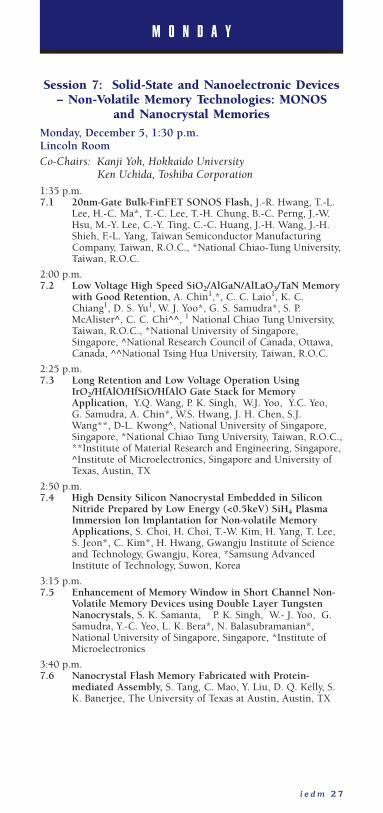
Session 7: Solid-State and Nanoelectronic Devices– Non-Volatile Memory Technologies: MONOS
and Nanocrystal MemoriesMonday, December 5, 1:30 p.m. Lincoln RoomCo-Chairs: Kanji Yoh, Hokkaido University
Ken Uchida, Toshiba Corporation
1:35 p.m.7.1 20nm-Gate Bulk-FinFET SONOS Flash, J.-R. Hwang, T.-L.
Lee, H.-C. Ma*, T.-C. Lee, T.-H. Chung, B.-C. Perng, J.-W.Hsu, M.-Y. Lee, C.-Y. Ting, C.-C. Huang, J.-H. Wang, J.-H.Shieh, F.-L. Yang, Taiwan Semiconductor ManufacturingCompany, Taiwan, R.O.C., *National Chiao-Tung University,Taiwan, R.O.C.
2:00 p.m.7.2 Low Voltage High Speed SiO2/AlGaN/AlLaO3/TaN Memory
with Good Retention, A. Chin1,*, C. C. Laio1, K. C.Chiang1, D. S. Yu1, W. J. Yoo*, G. S. Samudra*, S. P.McAlister^, C. C. Chi^^, 1 National Chiao Tung University,Taiwan, R.O.C., *National University of Singapore,Singapore, ^National Research Council of Canada, Ottawa,Canada, ^^National Tsing Hua University, Taiwan, R.O.C.
2:25 p.m.7.3 Long Retention and Low Voltage Operation Using
IrO2/HfAlO/HfSiO/HfAlO Gate Stack for MemoryApplication, Y.Q. Wang, P. K. Singh, W.J. Yoo, Y.C. Yeo,G. Samudra, A. Chin*, W.S. Hwang, J. H. Chen, S.J.Wang**, D-L. Kwong^, National University of Singapore,Singapore, *National Chiao Tung University, Taiwan, R.O.C.,**Institute of Material Research and Engineering, Singapore,^Institute of Microelectronics, Singapore and University ofTexas, Austin, TX
2:50 p.m.7.4 High Density Silicon Nanocrystal Embedded in Silicon
Nitride Prepared by Low Energy (<0.5keV) SiH4 PlasmaImmersion Ion Implantation for Non-volatile MemoryApplications, S. Choi, H. Choi, T.-W. Kim, H. Yang, T. Lee,S. Jeon*, C. Kim*, H. Hwang, Gwangju Institute of Scienceand Technology, Gwangju, Korea, *Samsung AdvancedInstitute of Technology, Suwon, Korea
3:15 p.m.7.5 Enhancement of Memory Window in Short Channel Non-
Volatile Memory Devices using Double Layer TungstenNanocrystals, S. K. Samanta, P. K. Singh, W.- J. Yoo, G.Samudra, Y.-C. Yeo, L. K. Bera*, N. Balasubramanian*,National University of Singapore, Singapore, *Institute ofMicroelectronics
3:40 p.m.7.6 Nanocrystal Flash Memory Fabricated with Protein-
mediated Assembly, S. Tang, C. Mao, Y. Liu, D. Q. Kelly, S.K. Banerjee, The University of Texas at Austin, Austin, TX
Jp 14-62 10/10/05 11:05 AM Page 27
2 8 i e d m
M O N D A Y
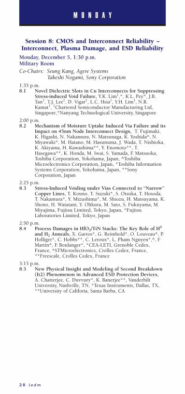
Session 8: CMOS and Interconnect Reliability –Interconnect, Plasma Damage, and ESD Reliability
Monday, December 5, 1:30 p.m.Military RoomCo-Chairs: Seung Kang, Agere Systems
Takeshi Nogami, Sony Corporation
1:35 p.m.8.1 Novel Dielectric Slots in Cu Interconnects for Suppressing
Stress-induced Void Failure, Y.K. Lim1,*, K.L. Pey*, J.B.Tan1, T.J. Lee1, D. Vigar1, L.C. Hsia1, Y.H. Lim1, N.R.Kamat1, 1Chartered Semiconductor Manufacturing Ltd,Singapore,*Nanyang Technological University, Singapore
2:00 p.m.8.2 Mechanism of Moisture Uptake Induced Via Failure and its
Impact on 45nm Node Interconnect Design, T. Fujimaki,K. Higashi, N. Nakamura, N. Matsunaga, K. Yoshida^, N.Miyawaki*, M. Hatano, M. Hasunuma, J. Wada, T. Nishioka,K. Akiyama, H. Kawashima**, Y. Enomoto**, T.Hasegawa**, K. Honda, M. Iwai, S. Yamada, F. Matsuoka,Toshiba Corporation, Yokohama, Japan, ^ToshibaMicroelectronics Corporation, Japan, *Toshiba InformationSystems Corporation, Yokohama, Japan, **SonyCorporation, Japan
2:25 p.m.8.3 Stress-Induced Voiding under Vias Connected to “Narrow”
Copper Lines, T. Kouno, T. Suzuki*, S. Otsuka, T. Hosoda,T. Nakamura*, Y. Mizushima*, M. Shiozu, H. Matsuyama, K.Shono, H. Watatani, Y. Ohkura, M. Sato, S. Fukuyama, M.Miyajima, Fujitsu Limited, Tokyo, Japan, *FujitsuLaboratories Limited, Tokyo, Japan
2:50 p.m.8.4 Process Damages in HfO2/TiN Stacks: The Key Role of H0
and H2 Anneals, X. Garros*, G. Reimbold*, O. Louveau^, P.Holliger*, C. Hobbs**, C. Leroux*, L. Pham Nguyen*,^, FMartin^, F. Boulanger*, *CEA-LETI, Grenoble Cedex,France, ^STMicroelectronics, Crolles Cedex, France,**Freescale, Crolles Cedex, France
3:15 p.m.8.5 New Physical Insight and Modeling of Second Breakdown
(It2) Phenomenon in Advanced ESD Protection Devices,A. Chatterjee, C. Duvvury*, K. Banerjee**, VanderbiltUniversity, Nashville, TN, *Texas Instruments, Dallas, TX,**University of Califoria, Santa Barba, CA
Jp 14-62 10/10/05 11:05 AM Page 28
i e d m 2 9
M O N D A Y
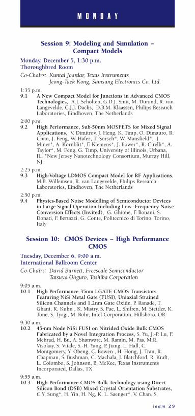
Session 9: Modeling and Simulation – Compact Models
Monday, December 5, 1:30 p.m.Thoroughbred RoomCo-Chairs: Kuntal Joardar, Texas Instruments
Jeong-Taek Kong, Samsung Electronics Co. Ltd.
1:35 p.m.9.1 A New Compact Model for Junctions in Advanced CMOS
Technologies, A.J. Scholten, G.D.J. Smit, M. Durand, R. vanLangevelde, C.J.J. Dachs, D.B.M. Klaassen, Philips ResearchLaboratories, Eindhoven, The Netherlands
2:00 p.m.9.2 High Performance, Sub-50nm MOSFETS for Mixed Signal
Applications, V. Dimitrov, J. Heng, K. Timp, O. Dimauro, R.Chan, J. Feng, W. Hafez, T. Sorsch*, W. Mansfield*, J.Miner*, A. Kornblit*, F. Klemens*, J. Bower*, R. Cirelli*, A.Taylor*, M. Feng, G. Timp, University of Illinois, Urbana,IL, *New Jersey Nanotechnology Consortium, Murray Hill,NJ
2:25 p.m.9.3 High-Voltage LDMOS Compact Model for RF Applications,
M.B. Willemsen, R. van Langevelde, Philips ResearchLaboratories, Eindhoven, The Netherlands
2:50 p.m.9.4 Physics-Based Noise Modelling of Semiconductor Devices
in Large-Signal Operation Including Low -Frequency NoiseConversion Effects (Invited), G. Ghione, F. Bonani, S.Donati, F. Bertazzi, G. Conte, Politecnico di Torino, Torino,Italy
Session 10: CMOS Devices – High PerformanceCMOS
Tuesday, December 6, 9:00 a.m. International Ballroom CenterCo-Chairs: David Burnett, Freescale Semiconductor
Tatsuya Ohguro, Toshiba Corporation
9:05 a.m.10.1 High Performance 35nm LGATE CMOS Transistors
Featuring NiSi Metal Gate (FUSI), Uniaxial StrainedSilicon Channels and 1.2nm Gate Oxide, P. Ranade, T.Ghani, K. Kuhn , K. Mistry, S. Pae, L. Shifren, M. Stettler, K.Tone, S. Tyagi, M. Bohr, Intel Corporation, Hillsboro, OR
9:30 a.m.10.2 45-nm Node NiSi FUSI on Nitrided Oxide Bulk CMOS
Fabricated by a Novel Integration Process, S. Yu, J.-P. Lu, F.Mehrad, H. Bu, A. Shanware, M. Ramin, M. Pas, M.R.Visokay, S. Vitale, S.-H. Yang, P. Jiang, L. Hall, C.Montgomery, Y. Obeng, C. Bowen , H. Hong, J. Tran, R.Chapman, S. Bushman, C. Machala, J. Blatchford, R. Kraft,L. Colombo, S. Johnson, B. McKee, Texas InstrumentsIncorporated, Dallas, TX
9:55 a.m.10.3 High Performance CMOS Bulk Technology using Direct
Silicon Bond (DSB) Mixed Crystal Orientation Substrates,C.Y. Sung*, H. Yin, H. Ng, K. L. Saenger*, V. Chan, S.
Jp 14-62 10/10/05 11:05 AM Page 29

3 0 i e d m
T U E S D A Y
Crowder, J. Li, J.A. Ott*, R. Bendernagel, J. Kempisty, V. Ku,H.K. Lee, Z.J. Luo, A. Madan, R.T. Mo, P. Nguyen, G. Pfeiffer,M. Raccioppo, N. Rovedo, D.K. Sadana*, J.P. de Souza*, R.Zhang, Z. Ren, C. Wann, IBM Semiconductor Research andDevelopment Center, Hopewell Junction, NY, *IBM T.J.Watson Research Center, Yorktown Heights, NY
10:20 a.m.10.4 High Performance CMOSFET Technology for 45nm
Generation and Scalability of Stress-Induced MobilityEnhancement Technique, A. Oishi, O. Fujii, T. Yokoyama*,K. Ota*, T. Sanuki, H. Inokuma, K. Eda, T. Idaka, H.Miyajima, S. Iwasa, H. Yamasaki, K. Oouchi, K. Matsuo, H.Nagano, T. Komoda, Y. Okayama, T. Matsumoto*, K.Fukasaku*, T. Shimizu, K. Miyano, T. Suzuki, K. Yahashi, A.Horiuchi*, Y. Takegawa, K. Saki, S. Mori, K. Ohno*, I.Mizushima, M. Saito*, M. Iwai, S. Yamada, N. Nagashima*, F.Matsuoka, Toshiba Corporation, Yokohama, Japan, *SonyCorporation, Yokohama, Japan
10:45 a.m.10.5 Integration and Optimization of Embedded-SiGe,
Compressive and Tensile Stressed Liner Films, and StressMemorization in Advanced SOI CMOS Technologies, M.Horstmann, A. Wei, T. Kammler, J. Höntschel, H. Bierstedt,H.-J. Engelmann, A. Hellmich, K. Hempel, G. Koerner, A.Neu, R. Otterbach, C. Reichel, M. Trentsch, P. Press, K.Frohberg, M. Schaller, H. Salz, J. Hohage, H. Ruelke, J. Klais,M. Raab , D. Greenlaw, N. Kepler, H. Chen*, D.Chidambarrao*, D. Fried*, J. Holt*, W. Lee*, H. Nii**, S.Panda*, T. Sato**, A. Waite^, S. Luning^, K. Rim*, D.Shepis*, M. Khare*, S.F. Huang*, J. Pellerin^, L.T. Su*, AMDSaxony LLC & Co., Dresden, Germany, *IBM Systems &Technology Group, Hopewell Junction, NY, **ToshibaAmerica Electronic Components Inc., Hopewell Junction, NY,^AMD Corporation, Hopewell Junction, NY
11:10 a.m.10.6 High Performance 30 nm Gate Bulk CMOS for 45nm Node
with �-shaped SiGe-SD, H. Ohta, Y. Kim, Y. Shimamune*, T.Sakuma, A. Hatada*, A. Katakami*, T. Soeda, K. Kawamura,H. Kokura, H. Morioka, T. Watanabe, J. Oh, Y. Hayami, J.Ogura, T. Mori, N. Tamura*, M. Kojima, T. Sugii*, K.Hashimoto, Fujitsu Limited, Tokyo, Japan, * FujitsuLaboratories Ltd., Tokyo, Japan
11:35 a.m.10.7 Record RF Performance of Sub-46nm Lgate NFETs in
Microprocessor SOI CMOS Technologies, S. Lee*, L.Wagner, B. Jaganathan, S. Csutak, J. Pekarik*, N. Zamdmer,M. Breitwisch, R. Ramachandran, G. Freeman, IBM Systemsand Technology Group, Hopewell Junction, NY, *IBMSystems and Technology Group, Essex Junction, VT
Jp 14-62 10/10/05 11:05 AM Page 30

i e d m 3 1
T U E S D A Y
Session 11: Solid-State and Nanoelectronic Devices– Nanotubes and Nanowires for Thermal and
Electrical ApplicationsTuesday, December 6, 9:00 a.m.International Ballroom EastCo-Chairs: Ali Javey, Stanford University
Ted Kamins, Hewlett Packard Labs
9:05 a.m.11.1 Carbon Nanotube Interconnects: Implications for
Performance, Power Dissipation and ThermalManagement, N. Srivastava, R. V. Joshi*, K. Banerjee,University of California, Santa Barba, CA, *IBM T. J. WatsonResearch Center, Yorktown Heights, NY
9:30 a.m.11.2 Electro-Thermal Transport in Metallic Single-Wall Carbon
Nanotubes for Interconnect Applications, E. Pop, D. Mann,J. Reifenberg, K. Goodson, H. Dai, Stanford University,Stanford, CA
9:55 a.m.11.3 Thermal and Source Bumps Utilizing Carbon Nanotubes
for Flip-chip High Power Amplifiers, T. Iwai*,1, H. Shioya*,D. Kondo*, S. Hirose*, A. Kawabata*, S. Sato*, M. Nihei*, T.Kikkawa1, K. Joshin1, Y. Awano*, N. Yokoyama*, *FujitsuLaboratories, Atsugi, Japan, 1Fujitsu Ltd., Atsugi, Japan
10:20 a.m.11.4 Nanoelectromechanical DRAM for Ultra-Large-Scale
Integration (ULSI), J.E. Jang, S.N. Cha, Y. Choi, D.J Kang,D.G. Hasko, J.E. Jung*, J.M. Kim*, G.A. J. Amaratunga,Cambridge University, Cambridge, U. K.,* SamsungAdvanced Institute of Technology, Yongin, Korea
10:45 a.m.11.5 Wrap-Gated InAs Nanowire Field Effect Transistor
(Invited), L.-E. Wernersson*,^, T. Bryllert*,#, E. Lind*, L.Samuelson*,^, *Lund University, Lund, Sweden, #ChalmersUniversity of Technology, Göteborg, Sweden, ^QuMatTechnologies AB, Lund, Sweden
11:10 a.m.11.6 A New Logic Family Based on Hybrid MOSFET-Polysilicon
Nano-Wires, S. Ecoffey, M. Mazza, V. Pott, D. Bouvet, A.Schmid, Y. Leblebici, M.J. Declercq, A.M. Ionescu, SwissFederal Institute of Technology, Lausanne, Switzerland
Jp 14-62 10/10/05 11:05 AM Page 31
3 2 i e d m
T U E S D A Y
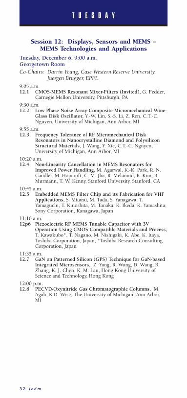
Session 12: Displays, Sensors and MEMS – MEMS Technologies and Applications
Tuesday, December 6, 9:00 a.m.Georgetown RoomCo-Chairs: Darrin Young, Case Western Reserve University
Juergen Brugger, EPFL
9:05 a.m.12.1 CMOS-MEMS Resonant Mixer-Filters (Invited), G. Fedder,
Carnegie Mellon University, Pittsburgh, PA
9:30 a.m.12.2 Low Phase Noise Array-Composite Micromechanical Wine-
Glass Disk Oscillator, Y.-W. Lin, S.-S. Li, Z. Ren, C.T.-C.Nguyen, University of Michigan, Ann Arbor, MI
9:55 a.m.12.3 Frequency Tolerance of RF Micromechanical Disk
Resonators in Nanocrystalline Diamond and PolysiliconStructural Materials, J. Wang, Y. Xie, C.T.-C. Nguyen,University of Michigan, Ann Arbor, MI
10:20 a.m.12.4 Non-Linearity Cancellation in MEMS Resonators for
Improved Power Handling, M. Agarwal, K.-K. Park, R. N.Candler, M. Hopcroft, C. M. Jha, R. Melamud, B. Kim, B.Murmann, T. W. Kenny, Stanford University, Stanford, CA
10:45 a.m.12.5 Embedded MEMS Filter Chip and its Fabrication for VHF
Applications, S. Mitarai, M. Tada, S. Yanagawa, T.Yamaguchi, T. Kinoshita, M. Tanaka, K. Ikeda, K. Yamashita,Sony Corporation, Kanagawa, Japan
11:10 a.m.12p6 Piezoelectric RF MEMS Tunable Capacitor with 3V
Operation Using CMOS Compatible Materials and Process,T. Kawakubo*, T. Nagano, M. Nishigaki, K. Abe, K. Itaya,Toshiba Corporation, Japan, *Toshiba Research ConsultingCorporation, Japan
11:35 a.m.12.7 GaN on Patterned Silicon (GPS) Technique for GaN-based
Integrated Microsensors, Z. Yang, R. Wang, D. Wang, B.Zhang, K. J. Chen, K. M. Lau, Hong Kong University ofScience and Technology, Hong Kong
12:00 p.m.12.8 PECVD-Oxynitride Gas Chromatographic Columns, M.
Agah, K.D. Wise, The University of Michigan, Ann Arbor,MI
Jp 14-62 10/10/05 11:05 AM Page 32
i e d m 3 3
T U E S D A Y
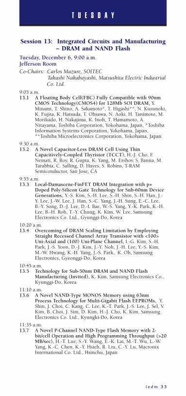
Session 13: Integrated Circuits and Manufacturing– DRAM and NAND Flash
Tuesday, December 6, 9:00 a.m.Jefferson RoomCo-Chairs: Carlos Mazure, SOITEC
Takashi Nakabayashi, Matsushita Electric IndustrialCo. Ltd. Co. Ltd.
9:05 a.m.13.1 A Floating Body Cell(FBC) Fully Compatible with 90nm
CMOS Technology(CMOS4) for 128Mb SOI DRAM, Y.Minami, T. Shino, A. Sakamoto*, T. Higashi**, N. Kusunoki,K. Fujita, K. Hatsuda, T. Ohsawa, N. Aoki, H. Tanimoto, M.Morikado, H. Nakajima, K. Inoh, T. Hamamoto, A.Nitayama, Toshiba Corporation, Yokohama, Japan, *ToshibaInformation Systems Corporation, Yokohama, Japan,**Toshiba Microelectronics Corporation, Yokohama, Japan
9:30 a.m.13.2 A Novel Capacitor-Less DRAM Cell Using Thin
Capacitively-Coupled Thyristor (TCCT), H.-J. Cho, F.Nemati, R. Roy, R. Gupta, K. Yang, M. Ershov, S. Banna, M.Tarabbia, C. Salling, D. Hayes, S. Robins, T-RAMSemiconductor, San Jose, CA
9:55 a.m.13.3 Local-Damascene-FinFET DRAM Integration with p+
Doped Poly-Silicon Gate Technology for Sub-60nm DeviceGenerations, Y.-S. Kim, S.-H. Lee, S.-H. Shin, S.-H. Han, J.-Y. Lee, J.-W. Lee, J. Han, S.-C. Yang, J.-H. Sung, E.-C. Lee,B.-Y. Song, D.-J. Lee, D.-I. Bae, W.-S. Yang, Y.-K. Park, K.-H.Lee, B.-H. Roh, T.-Y. Chung, K. Kim, W. Lee, SamsungElectronics Co. Ltd., Gyunggi-Do, Korea
10:20 a.m.13.4 Overcoming of DRAM Scaling Limitation by Employing
Straight Recessed Channel Array Transistor with <100>Uni-Axial and (100) Uni-Plane Channel, I.-G. Kim, S.-H.Park, J.-S. Yoon, D.-J. Kim, J.-Y. Noh, J.-H. Lee, Y.-S. Kim,M.-W. Hwang, K.-H. Yang, J.-S. Park, K. Oh, SamsungElectronics, Gyeonggi-Do, Korea
10:45 a.m.13.5 Technology for Sub-50nm DRAM and NAND Flash
Manufacturing (Invited), K. Kim, Samsung Electronics Co.,Kyunggi-Do, Korea
11:10 a.m.13.6 A Novel NAND-Type MONOS Memory using 63nm
Process Technology for Multi-Gigabit Flash EEPROMs, Y.Shin, J. Choi, C. Kang, C. Lee, K.-T. Park, J.-S. Lee, J. Sel, V.Kim, B. Choi, J. Sim, D. Kim, H.-J. Cho, K. Kim, SamsungElectronics Co. Ltd., Kyungki-Do, Korea
11:35 a.m.13.7 A Novel P-Channel NAND-Type Flash Memory with 2-
bit/cell Operation and High Programming Throughput (>20MB/sec), H.-T. Lue, S.-Y. Wang, E.-K. Lai, M.-T. Wu, L.-W.Yang, K.-C. Chen, K.-Y. Hsieh, R. Liu, C.-Y. Lu, MacronixInternational Co. Ltd., Hsinchu, Japan
Jp 14-62 10/10/05 11:05 AM Page 33

3 4 i e d m
T U E S D A Y
Session 14: Process Technology – Advanced Integration Concepts
Tuesday, December 6, 9:00 a.m.Lincoln RoomCo-Chairs: Simon Deleonibus, CEA/LETI
Sunit Tyagi, Intel Corporation
9:05 a.m.14.1 Challenges for the DRAM Cell Scaling to 40nm (Invited),
W. Mueller, W. Bergner, E. Erben, S. Jakschik, C. Kapteyn, A.Kersch, S. Kudelka, F. Lau, J. Luetzen, A. Orth, J. Nuetzel, J.Regul, T. Schloesser, A. Scholz, U. Schroeder, A. Sieck, A.Spitzer, M. Strasser, D. Temmler, P.F. Wang, S. Wege, R. Weis,Infineon Technologies, Dresden, Germany
9:30 a.m.14.2 Fabrication of 3D Trench PZT Capacitors for 256Mbit
FRAM Device Application, J.-M. Koo, B.-S. Seo, S. Kim, S.Shin, Jung-H. Lee, H. Baik, Jang-H. Lee, J.H. Lee, B.-J. Bae*,J.-E. Lim*, D.-C. Yoo*, S.-O. Park*, H.-S. Kim*, H. Han**,S. Baik**, J.-Y. Choi**, Y. J. Park**, Y. Park, SamsungAdvanced Institute of Technology, Kyungki-Do, Korea,*Samsung Electronics Co. Ltd., Kyungki-Do, Korea,**Pohang University of Science and Technology, Pohang,Korea
9:55 a.m.14.3 Highly Scalable Flash Memory with Novel Deep Trench
Isolation Embedded into High-Performance CMOS for the90nm Node & Beyond, D. Shum, A.T. Tilke, L. Pescini*,M. Stiftinger**, R. Kakoschke**, K.J. Han^, S.R. Kim^, V.Hecht^, N. Chan^, A. Yang^, R. Broze^, InfineonTechnologies North America, Hopewell Junction, NY,*Infineon Technologies Dresden GmbH & Co. OHG,Dresden, Germany, **Infineon Technologies AG, Munich,Germany, ^Actel Corporation, Mountain View, CA
10:20 a.m.14.4 New Three-Dimensional Integration Technology Using
Self-Assembly Technique, T. Fukushima, Y. Yamada, H.Kikuchi, M. Koyanagi, Tohoku University, Miyagi, Japan
10:45 a.m.14.5 Enabling SOI-Based Assembly Technology for Three-
Dimensional (3D) Integrated Circuits (ICs), A.W. Topol,D.C. La Tulipe, L. Shi, S.M. Alam, D.J. Frank, S.E. Steen, J.Vichiconti, D. Posillico, M. Cobb, S. Medd, S. Goma, D.DiMilia, M. T. Robson, E. Duch, M. Farinelli, C. Wang, R. A.Conti, D.M. Canaperi, L. Deligianni, A. Kumar, K.T.Kwietniak, C. D’Emic, J. Ott, A.M. Young , K. W. Guarini,M. Ieong, IBM T.J. Watson Research Center, YorktownHeights, NY
11:10 a.m.14.6 Self-Assembling Resists for Nanolithography (Invited), P.
F. Nealey, E. W. Edwards, M. Müller, M. P. Stoykovich, H.H.Solak*, J. J. de Pablo, University of Wisconsin-Madison,Madison, WI, *Paul Sherrer Institute, Villigen, Switzerland
Jp 14-62 10/10/05 11:05 AM Page 34

CCH
ECK
OOFF
RR EG
ISTR
ATIO
NTT Y
PEDD
ESIR
EDRR E
GIS
TRAT
ION
CCAT
EGO
RIES
AA DVA
NC
EBY
NNOV
..15
ON
SITE
TT OTA
LDD
UE
CConf
eren
ceTe
chni
calS
essi
onIE
EE M
embe
r__
___
$395
____
_ $4
35Fe
e in
clud
es e
ntra
nce
to M
on. -
Wed
. ses
sion
s, 1
cop
y of
No
n M
embe
r__
___
$485
__
___
$525
Tech
nica
l Dig
est,
one
CD-R
OM, a
nd o
ne ti
cket
for
Stud
ents
the
Mon
day
rece
ptio
n. D
OES
NOT
INCL
UDE
Mem
ber
____
_ $
50
____
_ $
50
ENTR
ANCE
TO
SHOR
T CO
URSE
S.No
n-M
embe
r__
___
$ 85
__
___
$ 85
TTota
lReg
istra
tion
Fee
Due
$
Shor
tCou
rses
- AD
VANC
E RE
GIST
RATI
ON IS
RECO
MM
ENDE
DLo
w Po
wer
____
_ $4
00__
___
$450
DUE
TOLI
MIT
EDSP
ACE.
Fee
incl
udes
ent
ranc
e to
one
Sho
rt Se
mi.
Mfg
____
_ $4
00__
___
$450
Cour
se, o
ne c
opy
of th
e Co
urse
wor
kboo
k, o
ne c
opy
of th
e Sh
ort
Cour
se C
D-RO
M a
nd C
ours
e lu
nche
on o
n Su
nday
. DOE
S NO
T IN
CLUD
E EN
TRAN
CE T
O TE
CHNI
CAL
SESS
IONS
.S St
uden
t -Lo
w Po
wer
____
_ $1
00
____
_ $1
00SSt
uden
t -Se
mi.
Mfg
____
_ $1
00__
___
$100
TTota
lSho
rtCo
urse
Regi
stra
tion
Due
$
Mis
cella
neou
s:Tu
esda
y Lu
nche
on__
___
$ 45
__
___
$ 45
Addi
tiona
l Tec
hnic
al D
iges
t__
___
$ 12
5 __
___
$ 12
5
TTota
lMis
cella
neou
sDu
e$
TOTA
LEN
CLOS
ED$ _
____
____
_
For O
ffice
Use
Onl
y
Chec
k #
Amou
nt $
Depo
sit D
ate
AD
VA
NC
E R
EG
IST
RA
TIO
N F
OR
M 2
005
Inte
rnat
iona
l Ele
ctro
n De
vice
s M
eeti
ngD
ecem
ber
5-7,
200
5, W
ashi
ngto
n, D
C •
Adva
nce
Dea
dlin
e: A
fter
Adva
nce
Reg
istr
atio
n D
eadl
ine
post
mar
ked
by N
ovem
ber
15pl
ease
reg
iste
r O
N S
ITE
STE
P 1
La
st N
ame
(Fam
ily N
ame)
......
......
......
......
......
......
......
......
......
....F
irst.
......
......
......
......
......
......
......
......
......
......
......
..In
itial
......
....
Com
pany
/Uni
vers
ity...
......
......
......
......
......
......
......
......
......
......
......
......
......
......
......
......
......
......
......
......
MS:
......
......
......
......
......
.....
Addr
ess.
......
......
......
......
......
......
......
......
......
......
......
......
......
......
......
......
......
......
......
......
......
......
......
......
......
......
......
......
......
......
...
City
......
......
......
......
......
......
......
......
......
......
......
......
......
...St
ate/
Coun
try...
......
......
......
......
......
......
....Z
ip C
ode.
......
......
......
......
.....
Phon
e (
)....
......
......
......
......
......
......
......
......
......
......
.Fax
(
)
......
......
......
......
......
......
......
......
......
......
......
......
......
......
......
.
Emai
l....
......
......
......
......
......
......
......
......
......
......
......
......
......
......
......
......
......
......
......
......
......
......
......
......
......
......
......
......
......
......
....
IEEE
Mem
ber N
o. .
......
......
......
......
......
......
......
......
......
......
......
......
......
......
......
...ED
S M
embe
r: __
____
_ Ye
s
___
____
No
(IEEE
Mem
ber G
rade
: __
____
_ M
embe
r
___
____
Sr.
Mem
ber
_
____
__ F
ello
w
___
____
Stu
dent
)
MMai
lthi
sfo
rman
dpa
ymen
tto:
IEDM
1622
0S.
Fred
eric
kRd
.Su
ite31
2,Ga
ither
sbur
g,M
D20
877,
USA
Fax:
301-
527-
0994
MMak
ech
ecks
paya
ble
to:I
EDM
•US
Fund
sON
LY,P
ayab
leon
aUS
Bank
• P
aym
ent m
ust b
e be
enc
lose
d to
pro
cess
this
form
• F
axes
acc
epte
d wi
th c
redi
t car
d pa
ymen
t ONL
Y.
• R
eque
sts
for c
ance
llatio
ns o
r ref
unds
mus
t be
rece
ived
by
Nov
embe
r 15,
200
5. A
$30
pro
cess
ing
fee
will
be w
ithhe
ld fr
om a
ll re
fund
s.
Tax
ID #
13-1
6566
33
DO
NO
TM
AIL
AN
D F
AX
TH
IS F
OR
M I
N—
IT W
ILL
RE
SU
LT I
N D
UP
LIC
AT
E C
HA
RG
ING
Paym
ent f
or re
gist
ratio
n m
ay b
e m
ade
by c
heck
(U.S
. Dol
lars
on
a U.
S. B
ank)
or c
redi
t car
d (M
aste
rcar
d or
Vis
a on
ly).
Chec
k of
f pay
men
t met
hod:
�
Che
ck e
nclo
sed
for a
mou
nt d
ue _
____
____
__or
�
Mas
terc
ard
� V
isa
Card
#__
____
____
____
____
____
____
____
____
____
____
____
__ E
xp. D
ate_
____
____
___
Sig
natu
re o
f Car
dhol
der_
____
____
____
____
____
____
____
____
____
____
____
____
Code
(3 n
umbe
rs o
n ba
ck o
f car
d)__
____
____
____
____
__
(Wor
k)(W
ork)
STEP
2
�
PPle
ase
type
orpr
int
Last
nam
e (fa
mily
nam
e)...
......
......
......
......
......
......
......
......
......
......
....F
irst .
......
......
......
......
......
......
......
......
......
.Initi
al...
......
......
......
......
......
......
Addr
ess.
......
......
......
......
......
......
......
......
......
......
......
......
......
......
......
......
......
......
......
......
......
......
......
......
......
......
..Mai
l Sto
p:...
......
......
......
......
....
......
......
......
......
......
......
......
......
......
......
......
......
......
......
......
......
......
......
......
......
......
......
......
......
......
......
......
......
......
......
......
......
......
......
......
......
...
Stat
e/Co
untry
......
......
......
......
......
......
......
......
......
......
......
......
......
......
......
......
......
......
......
......
......
......
......
......
......
Zip
Code
......
......
......
......
......
...
Tele
phon
e no
. (
)..
......
......
......
......
......
......
......
......
......
......
......
......
......
......
..Fa
x no
. (
).
......
......
......
......
......
......
......
......
......
......
..
Date
of A
rriva
l.....
......
......
......
......
......
......
......
......
......
......
......
......
......
......
......
......
...at
......
......
......
......
......
......
......
am/p
m...
......
......
......
......
......
....
Date
of D
epar
ture
......
......
......
......
......
......
......
......
......
......
......
......
......
......
......
......
...at
......
......
......
......
......
......
......
am/p
m...
......
......
......
......
......
....
Plea
se r
eser
ve a
ccom
mod
atio
ns a
s in
dica
ted:
____
___
Sing
le @
$18
6
___
____
Dou
ble
@ $
208
Chec
k of
f roo
m ty
pe d
esire
d. A
ll ro
oms
are
subj
ect t
o a
14.0
5% c
ity ta
x
RES
ERVA
TIO
N D
EAD
LIN
E:N
OV
EMB
ER 1
0, 2
005
afte
r w
hich
tim
e R
ATES
&AV
AILA
BILI
TY C
ANN
OT
BE G
UAR
ANTE
ED. R
oom
s m
ust b
e gu
aran
teed
by
a cr
edit
card
or
an a
dvan
ce d
epos
it. T
he h
otel
will
sen
d a
conf
irmat
ion.
GU
ARAN
TEED
RES
ERVA
TIO
NS:
Ind
icat
e on
e of
the
follo
win
g:
A. C
redi
t Car
d....
......
......
......
......
......
......
......
......
......
......
......
......
......
......
......
......
......
......
......
......
......
......
......
......
......
......
......
......
Card
Num
ber.
......
......
......
......
......
......
......
......
......
......
......
......
......
......
......
......
......
......
.Exp
. Dat
e....
......
......
......
......
......
......
......
..
Sign
atur
e....
......
......
......
......
......
......
......
......
......
......
......
......
......
......
......
......
......
......
......
......
......
......
......
......
......
......
......
......
......
..
B. F
irst N
ight
Dep
osit
Encl
osed
$ _
____
____
____
_
Mak
e ch
eck
paya
ble
to:
Hilt
on W
ashi
ngto
n (U
S do
llars
onl
y).
Mai
l or
fax
this
form
to th
e H
ilton
Was
hing
ton
to r
eser
ve a
roo
m u
nder
the
IED
M r
oom
blo
ck.(V
isa,
Am
eric
an E
xpre
ss...
)
MAI
L th
is fo
rm a
nd d
epos
it to
:
Res
erva
tion
sH
ilto
n W
ashi
ngto
n19
19 C
onne
ctic
ut A
venu
e, N
WW
ashi
ngto
n, D
C
2000
9 U
SA
Pho
ne:
202-
483-
3000
Fax:
202
-232
-043
8
2005
IEEE
Inte
rnat
iona
l Ele
ctro
n De
vice
s M
eeti
ngH
OT
EL
RE
GIS
TR
AT
ION
FO
RM
Dec
embe
r 5-
7, 2
005,
Hilt
on W
ashi
ngto
n, W
ashi
ngto
n, D
C
TTitle
(requ
ired
for m
embe
r rat
es)
Jp Reservation Foldout 10/6/05 8:57 AM Page 1
1. Separate the forms.
2. Send (mail or fax) the conference registration form to the conference office.
3. Send (mail or fax) the hotel reservationsform to the Hilton Washington
Do not send your hotel reservations form to the conference office. Send it only to the Hilton Washington and Towers.
iedmiedmAdvanc e Re s e r v a t i o n F o rmand Ho t e l R e s e r v a t i o n F o rm
Open Here for:
Jp Reservation Foldout 10/6/05 8:57 AM Page 2

i e d m 3 5
T U E S D A Y
Session 15: Quantum, Power, and CompoundSemiconductor Devices
Tuesday, December 6, 9:00 a.m. Military RoomCo-Chairs: Helmut Brech, Freescale Semiconductor
Yutaka Hoshino, Renesas Technology Corporation
9:05 a.m.15.1 High Frequency Power LDMOS Technologies for Base
Station Applications Staus, Potential, and Benchmarking(Invited), G. Ma, Q. Chen**, O. Tornblad^, T. Wei^, C.Ahrens*, B. Goebel*, C. Kuehn*, U. Seidel*, InfineonTechnologies, Tempe, AZ, *Infineon Technologies, Munich,Germany, **Infineon Technologies, Kista, Sweden, ^InfineonTechnologies, Morgan Hill, CA
9:30 a.m.15.2 High Performance RF Power LDMOSFETs for Cellular
Handsets Formed in Thick-Strained-Si/Relaxed-SiGeStructure, M. Kondo, N. Sugii*, Y. Hoshino, W.Hirasawa**, Y. Kimura*, M. Miyamoto, T. Fujioka, S.Kamohara, Y. Kondo, S. Kimura*, I. Yoshida, RenesasTechnology Corporation, Tokyo, Japan, *Hitachi Ltd., Japan,**Renesas Eastern Japan Semiconductor Inc., Japan
9:55 a.m.15.3 Performance and Limitations of 65 nm CMOS for
Integrated RF Power Applications, J. Scholvin, D.R.Greenberg*, J.A. del Alamo, MIT, Cambridge, MA, *IBMResearch, Hopewell Junction, NY
10:20 a.m.15.4 Dielectric Resurf: Breakdown Voltage Control by STI
Layout in Standard CMOS, J. Sonsky, A. Heringa, PhilipsResearch, Leuven, Belgium
10:45 a.m.15.5 AlGaN/GaN Devices for Power Switching Systems
(Invited), D. Ueda, T. Murata, M. Hikita, M. Yanagihara, S.Nakazawa, K. Inoue, H. Ishida, Y. Uemoto, T. Tanaka, T.Egawa*, Matsushita Electric Industrial Co. Ltd., Osaka,Japan, *Nagoya Institute of Technology, Osaka, Japan
11:10 a.m.15.6 A Low On-Resistance High Voltage SOI LIGBT with Oxide
Trench in Drift Region and Hole Bypass GateConfiguration, D. H. Lu, S. Jimbo, N. Fujishima, FujiElectric Advanced Technology Co. Ltd., Nagano, Japan
Jp 14-62 10/10/05 11:05 AM Page 35
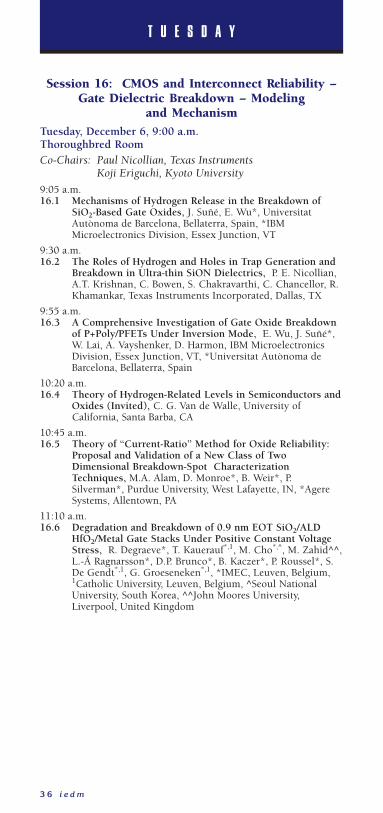
3 6 i e d m
T U E S D A Y
Session 16: CMOS and Interconnect Reliability –Gate Dielectric Breakdown – Modeling
and MechanismTuesday, December 6, 9:00 a.m. Thoroughbred RoomCo-Chairs: Paul Nicollian, Texas Instruments
Koji Eriguchi, Kyoto University
9:05 a.m.16.1 Mechanisms of Hydrogen Release in the Breakdown of
SiO2-Based Gate Oxides, J. Suñé, E. Wu*, UniversitatAutònoma de Barcelona, Bellaterra, Spain, *IBMMicroelectronics Division, Essex Junction, VT
9:30 a.m.16.2 The Roles of Hydrogen and Holes in Trap Generation and
Breakdown in Ultra-thin SiON Dielectrics, P. E. Nicollian,A.T. Krishnan, C. Bowen, S. Chakravarthi, C. Chancellor, R.Khamankar, Texas Instruments Incorporated, Dallas, TX
9:55 a.m.16.3 A Comprehensive Investigation of Gate Oxide Breakdown
of P+Poly/PFETs Under Inversion Mode, E. Wu, J. Suñé*,W. Lai, A. Vayshenker, D. Harmon, IBM MicroelectronicsDivision, Essex Junction, VT, *Universitat Autònoma deBarcelona, Bellaterra, Spain
10:20 a.m.16.4 Theory of Hydrogen-Related Levels in Semiconductors and
Oxides (Invited), C. G. Van de Walle, University ofCalifornia, Santa Barba, CA
10:45 a.m.16.5 Theory of “Current-Ratio” Method for Oxide Reliability:
Proposal and Validation of a New Class of TwoDimensional Breakdown-Spot CharacterizationTechniques, M.A. Alam, D. Monroe*, B. Weir*, P.Silverman*, Purdue University, West Lafayette, IN, *AgereSystems, Allentown, PA
11:10 a.m.16.6 Degradation and Breakdown of 0.9 nm EOT SiO2/ALD
HfO2/Metal Gate Stacks Under Positive Constant VoltageStress, R. Degraeve*, T. Kauerauf*,1, M. Cho*,^, M. Zahid^^,L.-Å Ragnarsson*, D.P. Brunco*, B. Kaczer*, P. Roussel*, S.De Gendt*,1, G. Groeseneken*,1, *IMEC, Leuven, Belgium,1Catholic University, Leuven, Belgium, ^Seoul NationalUniversity, South Korea, ^^John Moores University,Liverpool, United Kingdom
Jp 14-62 10/10/05 11:05 AM Page 36

i e d m 3 7
T U E S D A Y
Luncheon SessionTuesday, December 6, 12:20 p.m.International Ballroom WestLuncheon Presentation: “Bits and Atoms”
Prof. Neil Gershenfeld, MassachusettsInstitute of Technology
Professor Gershenfeld will discuss emerging insights into therelationship between the digital world of bits and the physicalworld of atoms: "building with logic" (programmed assembly, tofabricate perfect macroscopic structures out of imperfectmicroscopic components) and "programming with math"(compiling mathematical programs into distributed physicaldynamics, for engineering in a limit of thermodynamic complexity).Applications include analog logic, interdevice internetworking,paintable computing, and personal fabrication in developed anddeveloping countries.
Prof. Neil Gershenfeld is the Director of MIT's Center for Bits andAtoms. His unique laboratory investigates the relationship betweenthe content of information and its physical representation, frommolecular quantum computers to virtuosic musical instruments.Technology from his lab has been seen and used in settingsincluding New York's Museum of Modern Art and rural Indianvillages, the White House/Smithsonian Millennium celebration andautomobile safety systems, the World Economic Forum and inner-city community centers, Las Vegas shows and Sami herds. He is theauthor of numerous technical publications, patents, and booksincluding "Fab," "When Things Start To Think," "The Nature ofMathematical Modeling," and "The Physics of InformationTechnology," and has been featured in media such as The New YorkTimes, The Economist, CNN, and the McNeil/Lehrer News Hour.Dr. Gershenfeld has a BA in Physics with High Honors fromSwarthmore College, a Ph.D. from Cornell University, was a JuniorFellow of the Harvard University Society of Fellows, and a memberof the research staff at Bell Labs.
Awards Presentation2005 IEEE Cledo Brunetti Award
2005 IEEE Andrew S. Grove Award
2005 IEEE Daniel E. Noble Award
Jp 14-62 10/10/05 11:05 AM Page 37
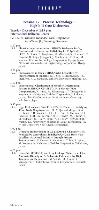
3 8 i e d m
T U E S D A Y
Session 17: Process Technology – High-k II Gate Dielectrics
Tuesday, December 6, 2:15 p.m.International Ballroom CenterCo-Chairs: Hirohito Watanabe, NEC Corporation
Gyo-Young Jin, Samsung Electronics
2:20 p.m.17.1 Fluorine Incorporation into HfSiON Dielectric for Vth
Control and Its Impact on Reliability for Poly-Si GatepFET, M. Inoue, S. Tsujikawa, M. Mizutani, K. Nomura*, T.Hayashi, K. Shiga, J. Yugami, J. Tsuchimoto, Y. Ohno, M.Yoneda, Renesas Technology Corporation, Hyogo, Japan,*Renesas Semiconductor Engineering Corporation, Hyogo,Japan
2:45 p.m.17.2 Improvement in High-k (HfO2/SiO2) Reliability by
Incorporation of Fluorine, K.-I. Seo, R. Sreenivasan, P. C.McIntyre, K. C. Saraswat, Stanford University, Stanford, CA
3:10 p.m.17.3 Experimental Clarification of Mobility Determining
Factors in HfSiON CMISFETs with Various FilmCompositions, R. Iijima, M. Takayanagi*, T. Yamaguchi, M.Koyama, A. Nishiyama, Toshiba Corporation, Yokohama,Japan, *Toshiba Corporation Semiconductor Company,Yokohama, Japan
3:35 p.m.17.4 High Performance Gate First HfSiON Dielectric Satisfying
45nm Node Requirements, M. A. Quevedo-Lopez, S. A.Krishnan, P. D. Kirsch, H. J. Li, J. H. Sim, C. Huffman, J. J.Peterson, B .H. Lee, G. Pant*, B. E. Gnade*, M. J. Kim*, R.M. Wallace*, D. Guo**, H. Bu**, T.P. Ma**, SEMATECH,Austin, TX, *University of Texas at Dallas, Richardson, TX,**Yale University, New Haven, Connecticut
4:00 p.m.17.5 Dramatic Improvement of Ge pMOSFET Characteristics
Realized by Amorphous Zr-Silicate/Ge Gate Stack withExcellent Structural Stability through ProcessTemperatures, Y. Kamata, Y. Kamimuta, T. Ino, R. Iijima,M. Koyama, A. Nishiyama, Toshiba Corporation, Yokohama,Japan
4:25 p.m.17.6 Ultra thin (EOT=3Å) and Low Leakage Dielectrics of La-
Alminate Directly on Si Substrate Fabricated by HighTemperature Deposition, M. Suzuki, M. Tomita, T.Yamaguchi, N. Fukushima, Toshiba Corporation, Kawasaki,Japan
Jp 14-62 10/10/05 11:05 AM Page 38

i e d m 3 9
T U E S D A Y
Session 18: Emerging Technologies – Flexible Electronics
Tuesday, December 6, 2:15 p.m.International Ballroom EastChair: Veena Misra, North Carolina State University
2:20 p.m.18.1 Organic Thin Electronics (Invited), T. Jackson, Penn State
University, University Park, PA
2:45 p.m.18.2 Flexible, Large-Area Sensors and Actuators with Organic
Transistor Integrated Circuits (Invited), T. Someya*,^, T.Sakurai*, T. Sekitani*, *University of Tokyo, Tokyo, Japan,^CREST/JST, Tokyo Japan
3:10 p.m.18.3 Organic Circuits on Flexible Substrates (Invited), H.
Klauk, Max Planck Institute for Solid State Research,Stuttgart, Germany
3:35 p.m.18.4 Organic and Hybrid Organic/Inorganic Transistors for
Chemical and Bio Sensing (Invited), A. Dodabalapur, D.Sharma, L. Wang, C. Burham, D. Fine, The University ofTexas at Austin, Austin, TX
4:00 p.m.18p5 Materials and Patterning Techniques for Macroelectronics
(Invited), J. A. Rogers, University of Illinois, Urbana, IL
Session 19: Solid-State and Nanoelectronic Devices– Novel Device Concepts
Tuesday, December 6, 2:15 p.m.Georgetown RoomCo-Chairs: Mark Reed, Yale University
Zoran Krivokapic, AMD
2:20 p.m.19.1 A Novel Nonvolatile Memory with Spin Torque Transfer
Magnetization Switching: Spin-RAM, M. Hosomi, H.Yamagishi, T. Yamamoto, K. Bessho, Y. Higo, K. Yamane, H.Yamada, M. Shoji, H. Kano, Sony Corporation, Kanagawa,Japan
2:45 p.m.19.2 A New Nano-Electro-Mechanical Field Effect Transistor
(NEMFET) Design for Low-Power Electronics, H. Kam, D.Lee, R. Howe, T.-J. King, University of California, Berkeley,CA
3:10 p.m.19.3 Single Molecular Devices with Fullerenes and
OligoPhenyleneVinylene (OPV) Derivatives (Invited),A. Danilov1, *, S. Kafanov*, T. Bjørnholm1, S. Kubatkin*,
1University of Copenhagen, Denmark, *Chalmers Universityof Technology, Göteborg, Sweden
3:35 p.m.19.4 The Micro to Nano Addressing Block (MNAB), K.
Gopalakrishnan, R. S. Shenoy, C. Rettner, R. King, Y.Zhang*, B. Kurdi, L. D. Bozano, J. J. Welser, M. B.
Jp 14-62 10/10/05 11:05 AM Page 39

4 0 i e d m
T U E S D A Y
Rothwell*, M. Jurich, M. I. Sanchez, M. Hernandez, P. M.Rice, W. P. Risk, H. K. Wickramasinghe, IBM AlmadenResearch Center, San Jose, CA, *IBM T.J. Watson ResearchCenter, Yorktown Heights, NY
4:00 p.m.19.5 Three Terminal Solid-Electrolyte Nanometer Switch,
T. Sakamoto*,1, N. Banno*,1, N. Iguchi*, H. Kawaura*, S. Kaeriyama^, M. Mizuno^, K. Terabe1,^^, T. Hasegawa1,^^,M. Aono1,^^, *NEC Corporation, Ibaraki, Japan, 1ICORP-(JST), Kanagawa, Japan, ^NEC Corporation, Kanagawa,Japan, ^^National Institute of Material Science, Ibaraki,Japan
Session 20: CMOS Devices – Strained-Silicon Technology
Tuesday, December 6, 2:15 p.m.Jefferson RoomCo-Chairs: Yee-Chia Yeo, National University of Singapore
Howard C.-H. Wang, TSMC
2:20 p.m.20.1 Design of High Performance PFETs with Strained Si
Channel and Laser Anneal, Z. Luo, Y. Chong*, J. Kim^, N.Rovedo, B. Greene, S. Panda, T. Sato^^, J. Holt, D.Chidambarrao, J. Li, R. Davis, A. Madan, A. Turansky, O.Gluschenkov, R. Lindsay**, A. Ajmera, J. Lee*, S. Mishra*,R. Amos, D. Schepis, H. Ng, K. Rim, IBM System &Technology Group, Hopewell Junction, NY, *CharteredSemiconductor Manufacturing Ltd., Hopewell Junction, NY,**Infineon Technologies AG, Hopewell Junction, NY,^Samsung Electronics Co. Ltd., Hopewell Junction, NY,^^Toshiba America Electronic Components Inc. at IBMSRDC, Hopewell Junction, NY
2:45 p.m.20.2 Source/Drain Germanium Condensation for P-Channel
Strained Ultra-Thin Body Transistors, K.-J. Chui, K.-W.Ang, A. Madan, G. H. Wang, C.-H. Tung*, L.-Y. Wong*, Y.Wang*, S.-F. Choy*, N. Balasubramanian*, M. F. Li , G.Samudra, Y.-C. Yeo, National Unversity of Singapore,Singapore, *Institute of Microelectronics, Singapore
3:10 p.m.20.3 Thin Body Silicon-on-Insulator N-MOSFET with Silicon-
Carbon Source/Drain Regions for PerformanceEnhancement, K.-W. Ang, K.-J. Chui, V. Bliznetsov*, Y.Wang*, L.-Y. Wong*, C.-H. Tung*, N. Balasubramanian*,M.-F. Li, G. Samudra, Y.-C. Yeo, National University ofSingapore, Singapore, *Institute of Microelectronics,Singapore
3:35 p.m.20.4 New Stress Inducing Technique of Epitaxial Si on Recessed
S/D Fabricated in Substrate Strained-Si of <100>-Channelon Rotated Wafers, T. Sanuki, H. Tanaka, K. Oota*, O.Fujii, R. Yamaguchi, K. Nakayama, Y. Morimasa, Y. Takasu,J. Idebuchi, N. Nishiyama, H. Fukui, H. Yoshimura, K.Matsuo, I. Mizushima, H. Ito, Y. Takegawa, M. Saito*, M.Iwai, N. Nagashima*, F. Matsuoka, Toshiba Corporation,Yokohama, Japan, *Sony Corporation, Yokohama, Japan
Jp 14-62 10/10/05 11:05 AM Page 40

T U E S D A Y
4:00 p.m.20.5 Stress Memorization in High-Performance FDSOI Devices
with Ultra Thin Silicon Channels and 25nm Gate Lengths,D. V. Singh, J. W. Sleight *, J. M. Hergenrother, Z. Ren* , K.A. Jenkins, O. Dokumaci* , L. Black**, J. B. Chang, H.Nakayama^, D. Chidambarrao* , R. Venigalla* , J. Pan**, W.Natzle, B. L. Tessier*, A. Nomura**, J. A. Ott, M. Ieong*, W.Haensch, IBM Semiconductor Research and DevelopmentCenter, Yorktown Heights, NY, *IBM Systems andTechnology Group, Hopewell Junction, NY, **AdvancedMicro Devices Inc., Hopewell Junction, NY, ^SonyElectronics Inc., Hopewell Junction, NY
4:25 p.m.20.6 Uniaxial-Biaxial Stress Hybridization For Super-Critical
Strained-Si Directly On Insulator (SC-SSOI) PMOS WithDifferent Channel Orientations, A.V-Y. Thean, L. Prabhu, V.Vartanian, M. Ramon, B-Y. Nguyen, T. White, H. Collard, Q-H Xie, S. Murphy, J. Cheek, S. Venkatesan, J. Mogab, C.H.Chang*, Y.H. Chiu*, H.C. Tuan*, Y.C. See*, M.S. Liang*,Y.C. Sun*, Freescale Semiconductor Inc., Austin, TX,*TSMC, Taiwan, R.O.C.
4:50 p.m.20.7 Dislocation Engineering in Strained MOS Materials
(Invited), E.A. Fitzgerald, M.L. Lee, D. Isaacson, D.A.Antoniadis, T.A. Langdo, MIT, Cambridge, MA
Session 21: Modeling and Simulation – Nanowires and Nanotubes
Tuesday, December 6, 2:15 p.m.Lincoln RoomCo-Chairs: Gerhard Klimeck, Purdue University
Mark Stettler, Intel Corporation
2:20 p.m.21.1 Computational Study of Carbon Nanotube p-i-n Tunnel
FETs, S. O. Koswatta, D. E. Nikonov*, M. S. Lundstrom,Purdue University, West Lafayette, IN, *Intel Corporation,Santa Clara, CA
2:45 p.m.21.2 Performance of Carbon Nanotube Field Effect Transistors
with Doped Source and Drain Extensions and ArbitraryGeometry, G. Fiori, G.Iannaccone, G. Klimeck*, Universitadegli Studi di Pisa, Pisa, Italy, *Purdue University, WestLafayette, IN
3:10 p.m.21.3 Ballistic Transport in Si, Ge, and GaAs Nanowire
MOSFETs, M. Bescond, N. Cavassilas*, K. Kalna, K.Nehari*, L. Raymond*, J. L. Autran*, M. Lannoo*, A.Asenov, University of Glasgow, Scotland, *LaboratoireMateriaux et Microelectronique de Provence, Marseille,France
3:35 p.m.21.4 Bandstructure and Orientation Effects in Ballistic Si and
Ge Nanowire FETs, J. Wang, A. Rahman, G. Klimeck, M.Lundstrom, Purdue University, West Lafayette, IN
4:00 p.m.21.5 Performance Assessment of Sub-Percolating Nanobundle
i e d m 4 1
T U E S D A Y
Jp 14-62 10/10/05 11:05 AM Page 41
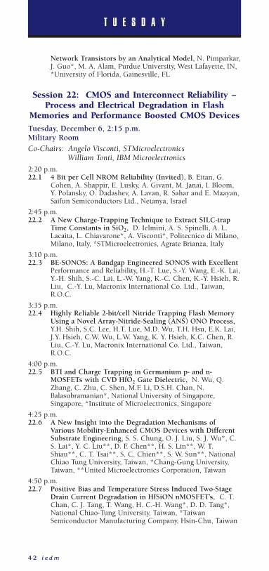
4 2 i e d m
T U E S D A Y
Network Transistors by an Analytical Model, N. Pimparkar,J. Guo*, M. A. Alam, Purdue University, West Lafayette, IN,*University of Florida, Gainesville, FL
Session 22: CMOS and Interconnect Reliability –Process and Electrical Degradation in Flash
Memories and Performance Boosted CMOS DevicesTuesday, December 6, 2:15 p.m.Military RoomCo-Chairs: Angelo Visconti, STMicroelectronics
William Tonti, IBM Microelectronics
2:20 p.m.22.1 4 Bit per Cell NROM Reliability (Invited), B. Eitan, G.
Cohen, A. Shappir, E. Lusky, A. Givant, M. Janai, I. Bloom,Y. Polansky, O. Dadashev, A. Lavan, R. Sahar and E. Maayan,Saifun Semiconductors Ltd., Netanya, Israel
2:45 p.m.22.2 A New Charge-Trapping Technique to Extract SILC-trap
Time Constants in SiO2, D. Ielmini, A. S. Spinelli, A. L.Lacaita, L. Chiavarone*, A. Visconti*, Politecnico di Milano,Milano, Italy, *STMicroelectronics, Agrate Brianza, Italy
3:10 p.m.22.3 BE-SONOS: A Bandgap Engineered SONOS with Excellent
Performance and Reliability, H.-T. Lue, S.-Y. Wang, E.-K. Lai,Y.-H. Shih, S.-C. Lai, L.-W. Yang, K.-C. Chen, K.-Y. Hsieh, R.Liu, C.-Y. Lu, Macronix International Co. Ltd., Taiwan,R.O.C.
3:35 p.m.22.4 Highly Reliable 2-bit/cell Nitride Trapping Flash Memory
Using a Novel Array-Nitride-Sealing (ANS) ONO Process,Y.H. Shih, S.C. Lee, H.T. Lue, M.D. Wu, T.H. Hsu, E.K. Lai,J.Y. Hsieh, C.W. Wu, L.W. Yang, K. Y. Hsieh, K.C. Chen, R.Liu, C.-Y. Lu, Macronix International Co. Ltd., Taiwan,R.O.C.
4:00 p.m.22.5 BTI and Charge Trapping in Germanium p- and n-
MOSFETs with CVD HfO2 Gate Dielectric, N. Wu, Q.Zhang, C. Zhu, C. Shen, M.F. Li, D.S.H. Chan, N.Balasubramanian*, National University of Singapore,Singapore, *Institute of Microelectronics, Singapore
4:25 p.m.22.6 A New Insight into the Degradation Mechanisms of
Various Mobility-Enhanced CMOS Devices with DifferentSubstrate Engineering, S. S. Chung, O. J. Liu, S. J. Wu*, C.S. Lai*, Y. C. Liu**, D. F. Chen**, H. S. Lin**, W. T.Shiau**, C. T. Tsai**, S. C. Chien**, S. W. Sun**, NationalChiao Tung University, Taiwan, *Chang-Gung University,Taiwan, **United Microelectronics Corporation, Taiwan
4:50 p.m.22.7 Positive Bias and Temperature Stress Induced Two-Stage
Drain Current Degradation in HfSiON nMOSFET’s, C. T.Chan, C. J. Tang, T. Wang, H. C.-H. Wang*, D. D. Tang*,National Chiao-Tung University, Taiwan, *TaiwanSemiconductor Manufacturing Company, Hsin-Chu, Taiwan
Jp 14-62 10/10/05 11:05 AM Page 42
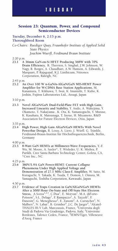
i e d m 4 3
T U E S D A Y
Session 23: Quantum, Power, and CompoundSemiconductor Devices
Tuesday, December 6, 2:15 p.m.Thoroughbred RoomCo-Chairs: Ruediger Quay, Fraunhofer Institute of Applied Solid
State PhysicsJoachim Wuerfl, Ferdinand Braun Institute
2:20 p.m.23.1 A 36mm GaN-on-Si HFET Producing 368W with 70%
Drain Efficiency, R. Therrien, S. Singhal, J.W. Johnson, W.Nagy, R. Borges, A. Chaudhari, A.W. Hanson, A. Edwards, J.Marquart, P. Rajagopal, K.J. Linthicum, NitronexCorporation, Raleigh, NC
2:45 p.m.23.2 An Over 100 W n-GaN/n-AlGaN/GaN MIS-HEMT Power
Amplifier for W-CDMA Base Station Applications, M.Kanamura, T. Kikkawa, T. Iwai, K. Imanishi, T. Kubo, K.Joshin, Fujitsu Laboratories Ltd., Atsugi, Japan
3:10 p.m.
23.3 Novel AlGaN/GaN Dual-Field-Plate FET with High Gain,Increased Linearity and Stability, Y. Ando, A. Wakejima, Y.Okamoto, T. Nakayama , K. Ota, K. Yamanoguchi, Y. Murase,K. Kasahara, K. Matsunaga, T. Inoue, H. Miyamoto, R&DAssociation for Future Electron Devices, Otsu, Japan
3:35 p.m.23.4 High Power, High Gain AlGaN/GaN HEMTs With Novel
Powerbar Design, R. Lossy, A. Liero, J. Würfl. G. Tränkle,Ferdinand-Braun-Institut für Höchstfrequenztechnik, Berlin,Germany
4:00 p.m.23.5 8-Watt GaN HEMTs at Millimeter-Wave Frequencies, Y.-F.
Wu, M. Moore, A. Saxler*, T. Wisleder, U. K. Mishra, P.Parikh, Cree Santa Barbara Technology Center, Goleta, CA,*Cree Inc., NC
4:25 p.m.23.6 380V/1.9A GaN Power-HEMT: Current Collapse
Phenomena Under High Applied Voltage andDemonstration of 27.1 MHz Class-E Amplifier, W. Saito, M.Kuraguchi, Y. Takada, K. Tsuda, T. Domon, I. Omura, M.Yamaguchi, Toshiba Corporation, Kawasaki, Japan
4:50 p.m.23.7 Evidence of Traps Creation in GaN/AlGaN/GaN HEMTs
After a 3000 Hour On-State and Off-State Hot ElectronStress, A.Sozza1,2,3, C.Dua1, E. Morvan1, M.A. diForte-Poisson1, S.L. Delage1, F. Rampazzo2, A. Tazzoli2, F.Danesin2, G. Meneghesso2, E. Zanoni2, A. Curutchet3, N.Malbert3, N. Labat3, B. Grimber4, J.C. De Jaeger4, 1Alcatel-THALES III-V Lab, Marcoussis, France, 2Universita degliStudi di Padova Via Gradenigo, Padova, Italy, 3UniversiteBordeaux, Talence Cedex, France, 4IEMN/Tiger, Villeneuved’Ascq, France
Jp 14-62 10/10/05 11:05 AM Page 43

4 4 i e d m
T U E S D A Y
Session 24: 2005 IEDM Evening Panel DiscussionTuesday, December 6, 8:00 p.m.International Ballroom CenterSemiconductor Research & Development: Who will do it and whowill pay for it in 2010?Moore’s clock is still the major driver of our industry. But thegrowing technical requirements make manufacturing facilitiesincreasingly expensive. This has caused a rising number ofmanufacturing joint ventures. But as R&D budgets are increasingfaster than chip makers’ revenues, and since we don’t want to slowdown Moore’s clock, R&D is consolidating in major initiatives andinstitutes. As the industry is confronting the challenges of thecoming 450mm wafer generation and of replacing the CMOStransistor by a “new switch”, some questions seem legitimate: canwe afford to slow down the clock? or will the consolidationcontinue? And if so, will this result in the ultimate global “public-private partnership”, necessary to preserve the productivity gainsthat invigorate other sectors of the economy? What is the role ofthe equipment and material suppliers?
But there is another aspect that deserves attention. Everybody willagree that technological innovation is an important driver ofeconomic growth. But to what extent are the dynamics ofinnovation determined by the relations between states and regions,and between governments and firms? Is a “techno-national”approach preferred, in which a nation or region invest heavily inorder to exert control over the generation of semiconductorknowledge and attempts to acquire leadership or to avoiddelocalization of its industry? Is a “techno-globalist” approach tobe preferred, in which states will rather provide the necessaryinfrastructure for ambitious exploratory research while firms areresponsible for technology development? And where does scientificexcellence come into the picture? How long can companies do it ontheir own? What about industrial alliances? What about consortiaand/or research institutes? What is the best way to share the futurecosts of semiconductor R&D?
To debate these topics we have invited a distinguished panel ofleaders from industry and R&D organizations. Coming from Asia,Europe and the US they will be able to present a truly globalperspective on these important issues.
Moderator: Gilbert Declerck, IMECPanel Members:
Chun-Yen ChangNational Chiao Tung University
Paolo GarginiIntel
Giang DaoSematech
Hisatsune WatanabeSELETE
Arthur Del PradoASMI
Joel HartmanCrolles Alliance
Jack SunTSMC
Bernie MeyersonIBM
Joo-Tae MoonSamsung
Jp 14-62 10/10/05 11:05 AM Page 44
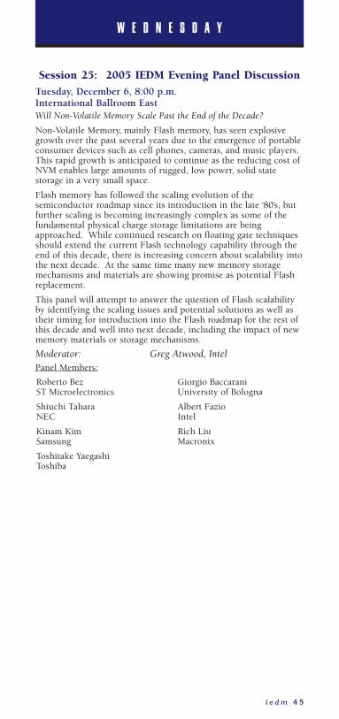
i e d m 4 5
W E D N E S D A Y
Session 25: 2005 IEDM Evening Panel DiscussionTuesday, December 6, 8:00 p.m.International Ballroom EastWill Non-Volatile Memory Scale Past the End of the Decade?
Non-Volatile Memory, mainly Flash memory, has seen explosivegrowth over the past several years due to the emergence of portableconsumer devices such as cell phones, cameras, and music players.This rapid growth is anticipated to continue as the reducing cost ofNVM enables large amounts of rugged, low power, solid statestorage in a very small space.
Flash memory has followed the scaling evolution of thesemiconductor roadmap since its introduction in the late ‘80’s, butfurther scaling is becoming increasingly complex as some of thefundamental physical charge storage limitations are beingapproached. While continued research on floating gate techniquesshould extend the current Flash technology capability through theend of this decade, there is increasing concern about scalability intothe next decade. At the same time many new memory storagemechanisms and materials are showing promise as potential Flashreplacement.
This panel will attempt to answer the question of Flash scalabilityby identifying the scaling issues and potential solutions as well astheir timing for introduction into the Flash roadmap for the rest ofthis decade and well into next decade, including the impact of newmemory materials or storage mechanisms.
Moderator: Greg Atwood, IntelPanel Members:
Roberto BezST Microelectronics
Shiuchi TaharaNEC
Kinam Kim Samsung
Toshitake Yaegashi Toshiba
Giorgio BaccaraniUniversity of Bologna
Albert FazioIntel
Rich Liu Macronix
Jp 14-62 10/10/05 11:05 AM Page 45

4 6 i e d m
T U E S D A Y
Session 26: Modeling and Simulation – Transportin Advanced Planar CMOS Devices
Wednesday, December 7, 9:00 a.m.International Ballroom WestCo-Chairs: Enrico Sangiorgi, University of Bologna
Martin Stadele, Infineon Technologies
9:05 a.m.26.1 First-Principles Modeling of Double-Gate UTSOI
MOSFETs, M. H. Evans*, M. Caussanel*, R. D. Schrimpf*,S. T. Pantelides*,^, *Vanderbilt University, Nashville, TN,^Oak Ridge National Laboratory, Oak Ridge, TN
9:30 a.m.26.2 Novel Channel Materials for Ballistic Nanoscale MOSFETs
Band Structure Effects, A. Rahman, G. Klimeck, M.Lundstrom, Purdue University, West Lafayette, IN
9:55 a.m.26.3 Investigation of Performance Limits of III-V Double-Gate
NMOSFETs, A. Pethe, T. Krishnamohan, D. Kim, S. Oh, H.-S. P. Wong, K. C. Saraswat, Stanford University, Stanford, CA
10:20 a.m.26.4 Scaling the High-Performance Double-Gate SOI MOSFET
Down to the 32 nm Technology Node with SiO2-BasedGate Stacks, N. Barin, M. Braccioli, C. Fiegna*, E.Sangiorgi*, University of Ferrara, Italy, *University ofBologno, Italy
10:45 a.m.26.5 A Study of the Effect of the Interface Roughness on a DG-
MOSFET Using a Full 2D NEGF Technique, A. Martinez,A. Svizhenko*, M. P. Anantram*, J. R. Barker, A. R. Brown,A. Asenov, University of Glasgow, Glasgow, United Kingdom,*NASA Ames Research Center, Moffet Field, CA
11:10 a.m.26.6 Multi-Subband Monte Carlo Modeling of Nano-MOSFETs
With Strong Vertical Quantization and Electron GasDegeneration, L. Lucci, P. Palestri, D. Esseni, L. Selmi,University of Udine, Udine, Italy
Session 27: Process Technology – Fully-Silicided Gates
Wednesday, December 7, 9:00 a.m.International Ballroom CenterCo-Chairs: Sunit Tyagi, Intel Corporation
S.C. Chen, TSMC9:05 a.m.
27.1 Physical Mechanism of Work Function Modulation Due toImpurity Pileup at Ni-FUSI/SiO(N) Interface, Y. Tsuchiya,M. Yoshiki, M. Koyama, A. Kinoshita, J. Koga, ToshibaCorporation, Yokohama, Japan
9:30 a.m.27.2 An Easily Integrable NiSi TOSI-Gate/SiON-Module for LP
SRAM Applications Based on a Single Step Silicidation ofGate and Junction, M. Müller, A. Mondot*, N. Gierczynski,D. Aimé*, B.Froment*, F. Leverd*, P. Gouraud*, A. Talbot*,S. Descombes**, Y. Morand*, G. Ribes*, J.-M. Roux*, S.
Jp 14-62 10/10/05 11:05 AM Page 46

i e d m 4 7
W E D N E S D A Y
Pokrant, F. André*, T.Skotnicki*, Philips Semiconductor,Crolles Cedex, France, *STMicroelectronics, Crolles Cedex,France, **CEA-LETI, Grenoble, France
9:55 a.m.27.3 Modulation of the Ni FUSI Workfunction of by Yb Doping:
from Midgap to N-Type Band-Edge, H.Y. Yu, J.D. Chen*,M.F. Li*, S.J. Lee*, D.L. Kwong^, M. van Dal**, J.A. Kittl, A.Lauwers, E. Augendre, S. Kubicek, C. Zhao, H. Bender, B.Brijs, L. Geenen, P. Absil, M. Jurczak, S. Biesemans, IMEC,Leuven, Belgium, *SNDL, Singapore, **Philips Research,Leuven, Belgium, ^University of Texas, Austin, TX
10:20 a.m.27.4 Lanthanide and Ir-based Dual Metal-Gate/HfAlON CMOS
with Large Work-Function Difference, D. S. Yu*, A.Chin*,#,C. H. Wu^, M.-F. Li#, C. Zhu#, S. J. Wang^, W. J. Yoo#, B. F.Hung*, S. P. McAlister^^, *National Chiao-Tung University,Taiwan, R.O.C., #National University of Singapore,Singapore, ^National Cheng Kung University, Taiwan,R.O.C., ^^National Research Council of Canada, Ottawa,Cananda
10:45 a.m.27.5 Demonstration of Ni Fully GermanoSilicide as a pFET
Gate Electrode Candidate on HfSiON, H.Y. Yu, R.Singanamalla, K. Opsomer, E. Augendre, E. Simoen, J.A.Kittl, S. Kubicek, S. Severi, X.P. Shi, S. Brus, C. Zhao, J.F. deMarneffe, S. Locorotondo, D. Shamiryan, M. Van Dal*, A.Veloso, A. Lauwers, M. Niwa, K. Maex, K. D. Meyer, P. Absil,M. Jurczak, S. Biesemans, IMEC, Leuven, Belgium, *PhilipsResearch, Leuven, Belgium
11:10 a.m.27.6 Systematic Study of Workfunction Engineering and
Scavenging Effect Using NiSi Alloy FUSI Metal Gates withAdvanced Gate Stacks, Y.H. Kim, C. Cabral, Jr., E.P. Gousev,R. Carruthers, L. Gignac, M. Gribelyuk, E. Cartier, S. Zarfar,M. Copel, V. Narayanan, J. Newbury, B. Price, J. Accevedo, P.Jamison, B. Linder, W. Natzle, J. Cai, R. Jammy, M. Ieong,IBM SRDC, Yorktown Heights, NY
11:35 a.m.27.7 CMOS Integration of Dual Work Function Phase
Controlled Ni FUSI with Simultaneous Silicidation ofNMOS (NiSi) and PMOS (Ni-rich silicide) Gates onHfSiON, A. Lauwers, A. Veloso, T. Hoffmann, M.J.H. vanDal, C. Vrancken, S. Brus, S. Locorotondo, J.-F. de Marneffe,B. Sijmus, S. Kubicek, T. Chiarella, M.A. Pawlak, K.Opsomer, M. Niwa, R. Mitsuhashi, K.G. Anil, H.Y. Yu, C.Demeurisse, R. Verbeeck, P. Absil, K. Maex, M. Jurczak, S.Biesemans, J. A. Kittl, IMEC, Leuven, Belgium
12:00 p.m.27.8 NixTa1-xSi and NixPt1-xSi Ternary Alloys for Work
Function Tuning on SiO2, HfSiOx and HfO2 Dielectrics, N.Biswas, S. Novak, M. Ozturk, V. Misra, North Carolina StateUniverisity, Raleigh, NC
Jp 14-62 10/10/05 11:05 AM Page 47

4 8 i e d m
W E D N E S D A Y
Session 28: Integrated Circuits and Manufacturing– Advanced SRAM and Novel Integration
TechnologyWednesday, December 7, 9:00 a.m. International Ballroom EastCo-Chairs: Tahir Ghani, Intel Corporation
Ted Houston, Texas Instruments, Inc.
9:05 a.m.28.1 Erratic Fluctuations of SRAM Cache Vmin at the 90nm
Process Technology Node, M. Agostinelli, J. Hicks, J. Xu, B.Woolery, K. Mistry, K. Zhang, S. Jacobs, J. Jopling, W. Yang,B. Lee, T. Raz, M. Mehalel, P. Kolar, Y. Wang, J. Sandford, D.Pivin, C. Peterson, M. DiBattista, S. Pae, M. Jones, S.Johnson, G. Subramanian, Intel Corporation, Hillsboro, OR
9:30 a.m.28.2 Fluctuation Limits and Scaling Opportunities for CMOS
SRAM Cells, A. Bhavnagarwala, S. Kosonocky, C. Radens*,K. Stawiasz, R. Mann*, Q. Ye*, K. Chin, IBM T.J. WatsonResearch Center, Yorktown Heights, NY, *IBM Systems &Technology Group, Hopewell Junction, NY
9:55 a.m.28.3 High Density and High Speed SRAM Bit-Cells and Ring
Oscillators due to Laser Annealing for 45nm Bulk CMOS,A. Pouydebasque, B. Dumont*, S. Denorme*, F. Wacquant*,M. Bidaud, C. Laviron^, A. Halimaoui*, C. Chaton^, J.D.Chapon*, P. Gouraud*, F. Leverd*, H. Bernard*, S.Warrick**, D. Delille, K. Romanjek, R. Gwoziecki^, N.Planes*, S. Vadot*, I. Pouilloux, F. Arnaud*, F. Boeuf*, T.Skotnicki*, Philips Semiconductors, Crolles, France,*STMicroelectronics, Crolles, France, **FreescaleSemiconductor, Crolles, France, ^CEA-LETI, Grenoble,France
10:20 a.m.28.4 Ultra-Fast Programming of Silicided Polysilicon Fuses
Based on New Insights in the Programming Physics, T.S.Doorn, M. Altheimer*, Philips Research, Eindhoven TheNetherlands, *Philips Semiconductors, Valbonne, France
10:45 a.m.28.5 Wafer-Level Compliant Bump for Three-Dimensional LSI
with High-Density Area Bump Connections, N. Watanabe,T. Kojima, T. Asano, Kyushu Institute of Technology,Fukuoka, Japan
11:10 a.m.28.6 Successful Transferring of Active Transistors, RF-Passive
Components and High Density Interconnect from Bulk Sito Organic Substrates, L. H. Guo, Q. X. Zhang, H. Y. Li, E.B. Liao, L. K. Bera, W. Y. Loh, C. C. Kuo, G. Q. Lo, N.Balasubramanian, D. L. Kwong, Institute ofMicroelectronics, Singapore
11:35 a.m.28.7 Fabrication and Characterization of CMOSFETs on Porous
Silicon for Novel Device Layer Transfer, H. Sanda, J.McVittie, M. Koto*, T. Yonehara*, Y. Nishi, StanfordUniversity, Stanford, CA, *Canon Inc., Kanagawa, Japan
Jp 14-62 10/10/05 11:05 AM Page 48

W E D N E S D A Y
Session 29: CMOS and Interconnect Reliability –Bias-Temperature Instability and Inteface Traps
Wednesday, December 7, 9:00 a.m.Georgetown RoomCo-Chairs: Ben Kaczer, IMEC
Ming-Fu Li, National University of Singapore andInstitute of Microelectronics Singapore
9:05 a.m.29.1 On the Dispersive Versus Arrhenius Temperature
Activation of NBTI Time Evolution in Plasma NitridedGate Oxides: Measurements, Theory, and Implications, D.Varghese, D. Saha, S. Mahapatra, K. Ahmed*, F. Nouri*, M.Alam**, IIT Bombay, Mumbai, India, *Applied Materials,CA, **Purdue University, West Lafayette, IN
9:30 a.m.29.2 Material Dependence of Hydrogen Diffusion and its
Implications for NBTI Degradation, A. T. Krishnan, C.Chancellor, S. Chakravarthi, P. E. Nicollian, V. Reddy, A.Varghese, R. B. Khamankar, S. Krishnan, Texas Instruments,Dallas, TX
9:55 a.m.29.3 Negative Bias Temperature Instability of Carrier-Transport
Enhanced pMOSFET with Performance Boosters, H. S.Rhee, H. Lee, T. Ueno, D. S. Shin, S. H. Lee, M. Kim, H. S.Kim, N.-I. Lee, Samsung Electronics Co. Ltd., Kyunggi-Do,Korea
10:20 a.m.29.4 Defect Passivation with Fluorine in a TaxCy/High-K Gate
Stack for Enhanced Device Threshold Voltage Stability andPerformance, H.-H. Tseng, P.J. Tobin, E. A. Hebert, S.Kalpat, M. E. Ramón, L. Fonseca, Z. X. Jiang, J. K. Schaeffer,R. I. Hegde, D. H. Triyoso, D. C. Gilmer, W. J. Taylor, C. C.Capasso, O. Adetutu, D. Sing, J. Conner, E. Luckowski, B.W. Chan, A. Haggag, S. Backer, R. Noble, M. Jahanbani, Y. H.Chiu, B. E. White, Freescale Semiconductor Inc., Austin, TX
10:45 a.m.29.5 Accurate Circuit Performance Prediction Model and
Lifetime Prediction Method of NBT Stressed Devices forHighly Reliable ULSI Circuits, R. Kuroda, K. Watanabe, A.Teramoto, M. Mifuji*, T. Yamaha*, S. Sugawa, T. Ohmi,Tohoku University, Sendai, Japan, *ROHM Co. Ltd.,Shizuoka, Japan
11:10 a.m.29.6 On-Chip Charge Pumping Method for Characterization of
Interface States of Ultra Thin Gate Oxide in Nano CMOSTechnology, H.-H. Ji, Y.-G. Kim, I.-S. Han, K.-M. Kim, J.-S.Wang, H.-D. Lee, S.-H. Park*, H.-S. Lee*,Y.-S. Kang*, D.-B.Kim*, C.-Y. Lee*, I.-H. Cho*, S.-Y. Kim*, S.-B. Hwang*, J.-G. Lee*, J.-W. Park*, Chungnam National University,Daejeon, Korea, *Magnachip Semiconductor Inc.,Choongbuk, Korea
i e d m 4 9
Jp 14-62 10/10/05 11:05 AM Page 49

W E D N E S D A Y
Session 30: CMOS Devices – SOI and Multi-GateDevices
Wednesday, December 7, 9:00 a.m.Jefferson Room
Co-Chairs: Hitoshi Wakabayashi, NEC CorporationSerge Biesemans, IMEC
9:05 a.m.30.1 High Performance Multi-Gate pMOSFETs using Uniaxially-
Strained SGOI Channels, T. Irisawa, T. Numata, T. Tezuka,K. Usuda, S. Nakaharai, N. Hirashita, N. Sugiyama, E.Toyoda*, S.-I Takagi**, MIRAI-ASET, **MIRAI-AIST,*Toshiba Corporation, Kawasaki, Japan
9:30 a.m.30.2 Inverted T Channel FET (ITFET) — Fabrication and
Characteristics of Vertical-Horizontal, Thin Body, Multi-Gate, Multi-Orientation Devices, ITFET SRAM Bit-CellOperation. A Novel Technology for 45nm and BeyondCMOS, L. Mathew, M. Sadd, S. Kalpat M. Zavala, T.Stephens, R. Mora, S. Bagchi, C. Parker, J. Vasek, D. Sing, R.Shimer, L. Prabhu, G.O. Workman, G. Ablen, Z.Shi, J. Saenz,B. Min, D. Burnett, B.-Y. Nguyen, J. Mogab, M.M.Chowdhury*, W. Zhang*, J.G. Fossum*, FreescaleSemiconductor Inc., Austin, TX, *University of Florida, FL
9:55 a.m.30.3 High Performance 5nm Radius Twin Silicon Nanowire
MOSFET(TSNWFET) : Fabrication on Bulk Si Wafer,Characteristics, and Reliability, S. D. Suk, S.-Y. Lee, S.-M.Kim, E.-J. Yoon, M.-S. Kim, M. Li, D.-S. Shin, K.-H. Lee, H.S. Park, J. N. Han, J.-B. Park, D.-W. Kim, D. Park, B.-I. Ryu,Samsung Electronics Co., Gyeonggi-Do, Korea
10:20 a.m.30.4 Process Integration Technology and Device Characteristics
of CMOS FinFET on Bulk Silicon Substrate with Sub-10nm Fin Width and 20nm Gate Length, K. Okano, T.Izumida, H. Kawasaki, A. Kaneko, A. Yagishita, T.Kanemura, M. Kondo, S. Ito, N. Aoki, K. Miyano, T. Ono, K.Yahashi, K. Iwade, T. Kubota, T. Matsushita, I. Mizushima, S.Inaba, K. Ishimaru, K. Suguro, K. Eguchi, Y. Tsunashima, H.Ishiuchi, Toshiba Corporation Semiconductor Company,Yokohama, Japan
10:45 a.m.30.5 GIDL (Gate-Induced Drain Leakage) and Parasitic
Schottky Barrier Leakage Elimination in AggressivelyScaled HfO2/TiN FinFET Devices, T. Hoffmann, G.Doornbos, I. Ferain, N. Collaert, P. Zimmerman, M.Goodwin, R. Rooyackers, K.G. Anil, Y. Yim, M. Jurczak, S.Biesemans, IMEC, Heverlee, Belgium
11:10 a.m.30.6 Mobility Enhancement due to Volume Inversion in (110)-
Oriented Ultra-thin Body Double-Gate nMOSFETs withBody Thickness Less Than 5 nm, G. Tsutsui, M. Saitoh, T.Saraya, T. Nagumo, T. Hiramoto, University of Tokyo,Tokyo, Japan
11:35 a.m.30.7 Selective Epitaxial Channel Ground Plane Thin SOI CMOS
Devices, Z. Ren, M. Ieong, J. Cai*, J. Holt, D. Boyd, R. Mo,H. Yin, O. Dokumaci, S. Kawanaka**, T. Sato**, P.
5 0 i e d m
Jp 14-62 10/10/05 11:05 AM Page 50
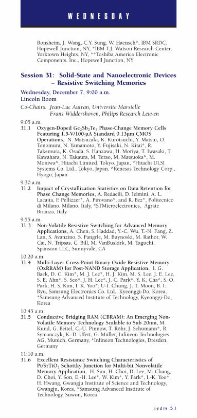
W E D N E S D A Y
Ronsheim, J. Wang, C.Y. Sung, W. Haensch*, IBM SRDC,Hopewell Junction, NY, *IBM T.J. Watson Research Center,Yorktown Heights, NY, **Toshiba America ElectronicComponents, Inc., Hopewell Junction, NY
Session 31: Solid-State and Nanoelectronic Devices– Resistive Switching Memories
Wednesday, December 7, 9:00 a.m.Lincoln RoomCo-Chairs: Jean-Luc Autran, Universite Marsielle
Frans Widdershoven, Philips Research Leuven
9:05 a.m.31.1 Oxygen-Doped Ge2Sb2Te5 Phase-Change Memory Cells
Featuring 1.5-V/100-µA Standard 0.13µm CMOSOperations, N. Matsuzaki, K. Kurotsuchi, Y. Matsui, O.Tonomura, N. Yamamoto, Y. Fujisaki, N. Kitai*, R.Takemura, K. Osada, S. Hanzawa, H. Moriya, T. Iwasaki, T.Kawahara, N. Takaura, M. Terao, M. Matsuoka^, M.Moniwa^, Hitachi Limited, Tokyo, Japan, *Hitachi ULSISystems Co. Ltd., Tokyo, Japan, ^Renesas Technology Corp.,Hyogo, Japan
9:30 a.m.31.2 Impact of Crystallization Statistics on Data Retention for
Phase Change Memories, A. Redaelli, D. Ielmini, A. L.Lacaita, F. Pellizzer*, A. Pirovano*, and R. Bez*, Politecnicodi Milano, Milano, Italy, *STMicroelectronics, AgrateBrianza, Italy.
9:55 a.m.31.3 Non-Volatile Resistive Switching for Advanced Memory
Applications, A. Chen, S. Haddad, Y.-C. Wu, T.-N. Fang, Z.Lan, S. Avanzino, S. Pangrle, M. Buynoski, M. Rathor, W.Cai, N. Tripsas, C. Bill, M. VanBuskirk, M. Taguchi,Spansion LLC, Sunnyvale, CA
10:20 a.m.31.4 Multi-Layer Cross-Point Binary Oxide Resistive Memory
(OxRRAM) for Post-NAND Storage Application, I. G.Baek, D. C. Kim*, M. J. Lee*, H. J. Kim, M. S. Lee, J. E. Lee,S. E. Ahn*, S. Seo*, J. H. Lee*, J. C. Park*, Y. K. Cha*, S. O.Park, H. S. Kim, I. K. Yoo*, U-I. Chung, J. T. Moon, B. I.Ryu, Samsung Electronics Co. Ltd., Kyeonggi-Do, Korea,*Samsung Advanced Institute of Technology, Kyeonggi-Do,Korea
10:45 a.m.31.5 Conductive Bridging RAM (CBRAM): An Emerging Non-
Volatile Memory Technology Scalable to Sub 20nm, M.Kund, G. Beitel, C.-U. Pinnow, T. Röhr, J. Schumann*, R.Symanczyk, K.-D. Ufert, G. Müller, Infineon TechnologiesAG, Munich, Germany, *Infineon Technologies, Dresden,Germany
11:10 a.m.31.6 Excellent Resistance Switching Characteristics of
Pt/SrTiO3 Schottky Junction for Multi-bit NonvolatileMemory Application, H. Sim, H. Choi, D. Lee, M. Chang,D. Choi, Y. Son, E.-H. Lee*, W. Kim*, Y. Park*, I.-K. Yoo*,H. Hwang, Gwangju Institute of Science and Technology,Gwangju, Korea, *Samsung Advanced Institute ofTechnology, Suwon, Korea
i e d m 5 1
Jp 14-62 10/10/05 11:05 AM Page 51

W E D N E S D A Y
Session 32: Quantum, Power, and Semiconductors Devices
Wednesday, December 7, 9:00 a.m.Military RoomCo-Chairs: Jesus del Alamo, Massachusetts Institute of
TechnologyTetsuya Suemitsu, NTT Photonics Laboratories
9:05 a.m.32.1 85nm Gate Length Enhancement and Depletion Mode InSb
Quantum Well Transistors for Ultra High Speed and VeryLow Power Digital Logic Applications, S. Datta, T. Ashley*,R. Chau, K. Hilton*, R. Jefferies*, T. Martin*, T. Phillips*,Intel Corporation, Hillsboro, OR, *QinetiQ, Malvern, UnitedKingdom
9:30 a.m.32.2 Performance Evaluation of 50 nm In0.7Ga0.3As HEMTs For
Beyond-CMOS Logic Applications, D. H. Kim, J. A. delAlamo, J. H. Lee*, K. S. Seo*, MIT, Cambridge, MA, *SeoulNational University, Seoul, Korea
9:55 a.m.32.3 Monolithic Integration of Enhancement- and Depletion-
mode AlGaN/GaN HEMTs for GaN Digital IntegratedCircuits, Y. Cai, Z. Cheng, W. C. W. Tang, K. J. Chen, K. M.Lau, Hong Kong University of Science and Technology, HongKong, R.O.C.
10:20 a.m.32.4 Laterally Scaled-Down Tiered-Edge-Shaped Ohmic
Structure of InP-based HEMTs for 2-S/mm gm and 500-GHz fT, H. Matsuzaki, T. Maruyama*, M. Tokumitsu, T.Enoki, NTT Corporation, Kanagawa, Japan, *NTT AdvancedTechnology Corporation, Kanagawa, Japan
10:45 a.m.32.5 The InP/GaAsSb Type-II Heterostructure System and its
Application to High-Speed DHBTs and Photodetectors:Physics, Surprises, and Opportunities (Invited), C.R.Bolognesi, H.G. Liu, D.W. DiSanto, N.G. Tao, L. Zheng, X.Zhang, S.P. Watkins, Simon Fraser University, Burnaby BC,Canada
11:10 a.m.32.6 Non-Uniform Degradation Behavior Across Device Width
in RF Power GaAs PHEMTs, A. A. Villanueva, J. A. delAlamo, T. Hisaka*, K. Hayashi*, M. Somerville**, MIT,Cambridge, MA, *Mitsubishi Electric, Hyogo, Japan, **OlinCollege, Needham, MA
5 2 i e d m
Jp 14-62 10/10/05 11:05 AM Page 52
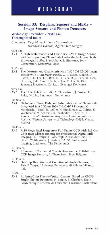
W E D N E S D A Y
Session 33: Displays, Sensors and MEMS – Image Sensors and Photon Detectors
Wednesday, December 7, 9:00 a.m.Thoroughbred RoomCo-Chairs: Keiji Mabuchi, Sony Corporation
Homayoon Haddad, Agilent Technologies
9:05 a.m.33.1 A High-Performance and Low-Noise CMOS Image Sensor
with an Expanding Photodiode Under the Isolation Oxide,K. Itonaga, H. Abe, I. Yoshihara, T. Hirayama, SonyCorporation, Kanagawa, Japan
9:30 a.m.33.2 The Features and Characteristics of 1/3” 5M CMOS Image
Sensor with 1.9x1.9µm2 Pixels, C.-R. Moon, J. Jung, D.Kwon, S.-H. Lee, J.-S. Roh, K.-H. Paik, D.-C. Park, H. Kim,H. Jeong, J.-H. Sim, H. Noh, K. Lee, D. Lee, K. Kim,Samsung Electronics Co. Ltd., Gyeonggi-Do, Korea
9:55 a.m.33.3 The Hole Role (Invited), A. Theuwissen, J. Bosiers, E.
Roks, DALSA, Eindhoven, Netherlands
10:20 a.m.33.4 High-Speed Blue-, Red-, and Infrared-Sensitive Photodiode
Integrated in a 0.35µm SiGe:C-BiCMOS Process, G.Meinhardt, J. Kraft, B. Löffler, H. Enichlmair, G. Röhrer, E.Wachmann, M. Schrems, R. Swoboda*, C. Seidl*, H.Zimmermann*, Austriamicrosystems, Unterpremstätten,Austria, *Vienna University of Technology-EMST, Vienna,Austria
10:45 a.m.33.5 A 28 Mega Pixel Large Area Full Frame CCD with 2x2 On-
Chip RGB Charge Binning for Professional Digital StillImaging, C. Draijer, F. Polderdijk, A. van der Heide, B.Dillen, W. Klaassens, J. Bosiers, DALSA ProfessionalImaging, Eindhoven, The Netherlands
11:10 a.m.33.6 Influence of Terrestrial Cosmic Rays on the Reliability of
CCD Image Sensors, A. Theuwissen, Bree, Belgium
11:35 a.m.33.7 On-Chip Detection and Counting of Single-Photons, S.
Tisa, F. Zappa, I. Labanca, Politecnico di Milano, Milano,Italy
12:00 p.m.33.8 An Intra-Chip Electro-Optical Channel Based on CMOS
Single Photon Detectors, M. Sergio, E. Charbon, EcolePolytechnique Federale de Lausanne, Lausanne, Switzerland
i e d m 5 3
Jp 14-62 10/10/05 11:05 AM Page 53

W E D N E S D A Y
Session 34: Process Techology – Advanced FEOL Technology
Wednesday, December 7, 1:30 p.m.International Ballroom WestCo-Chairs: Kyoichi Suguro, Toshiba Corporation
Mehmet Ozturk, North Carolina State University
1:35 p.m.34.1 A Simple Approach to Optimizing Ultra-thin SiON Gate
Dielectrics Independently for n- and p-MOSFETs, S.Tsujikawa, H. Umeda, T. Kawahara, Y. Kawasaki, K. Shiga, T.Yamashita, T. Hayashi, J. Yugami, Y. Ohno, M. Yoneda,Renesas Technology Corporation, Hyogo, Japan
2:00 p.m.34.2 Dramatic Improvement of Vfb Shift and Gm
max with Ultra-Thin and Ultra-Low-Leakage SiN-Based SiON GateDielectrics, D. Matsushita, K. Muraoka, Y. Nakasaki, K.Kato, S. Kikuchi, K. Sakuma, Y. Mitani, K. Eguchi, M.Takayanagi, Toshiba Corporation, Yokohama, Japan
2:25 p.m.34.3 Interface States as an Active Component for 20 nm Gate-
Length Planar MOSFET with ElectroStatic ChannelExtension (ESCE), G.H. Buh, T. Park, G.H. Yon, C.W.Ryoo, D.C. Kim, Y.G. Shin, U-I. Chung, J.T. Moon, SamsungElectronics Company, Kyunggi-Do, Korea
2:50 p.m.34.4 Single Stress Liner for Both NMOS and PMOS Current
Enhancement by a Novel Ultimate Spacer Process, Y. C.Liu, J.W. Pan, T.Y. Chang, P.W. Liu, B.C. Lan, C.H. Tung,C.H. Tsai, T.F. Chen, C.J. Lee, W.M. Wang, Y.A. Chen, H.L.Shih, L.Y. Tung, L.W. Cheng, T.M. Shen, S.C. Chiang, M.F.Lu, W.T. Chang, Y.H. L*, D. Nayak*, D. Gitlin*, H.L. Meng,C.T. Tsai, United Microelectronics Corporation, Hsin-Chu,Taiwan, *Xilinx, San Jose, CA
3:15 p.m.34.5 Damage-Free Neutral Beam Etching Technology for High
Mobility FinFETs, K. Endo, S. Noda*, M. Masahara, T.Kubota*, T. Ozaki*, S. Samukawa*, Y. Liu, K. Ishii, Y.Ishikawa, E. Sugimata, T. Matsukawa, H. Takashima, H.Yamauchi, E. Suzuki, National Institute of AdvancedIndustrial Science and Technology, Ibaraki, Japan, *TohokuUniversity, Miyagi, Japan
3:40 p.m.34.6 Sidewall Transfer Process and Selective Gate Sidewall
Spacer Formation Technology for Sub-15nm FinFET withElevated Source/Drain Extension, A. Kaneko, A. Yagishita,K. Yahashi, T. Kubota, M. Omura, K. Matsuo, I. Mizushima,K. Okano, H. Kawasaki, S. Inaba, T. Izumida, T. Kanemura,N. Aoki, K. Ishimaru, H. Ishiuchi, K. Suguro, K. Eguchi, Y.Tsunashima, Toshiba Corporation Semiconductor Company,Yokohama, Japan
5 4 i e d m
Jp 14-62 10/10/05 11:05 AM Page 54
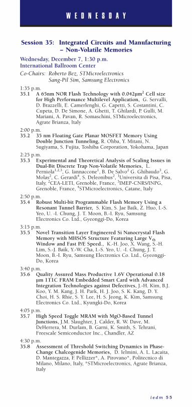
W E D N E S D A Y
Session 35: Integrated Circuits and Manufacturing– Non-Volatile Memories
Wednesday, December 7, 1:30 p.m.International Ballroom CenterCo-Chairs: Roberto Bez, STMicroelectronics
Sang-Pil Sim, Samsung Electronics
1:35 p.m.35.1 A 65nm NOR Flash Technology with 0.042µm2 Cell size
for High Performance Multilevel Application, G. Servalli,D. Brazzelli, E. Camerlenghi, G. Capetti, S. Costantini, C.Cupeta, D. De Simone, A. Ghetti, T. Ghilardi, P. Gulli, M.Mariani, A. Pavan, R. Somaschini, STMicroelectronics,Agrate Brianza, Italy
2:00 p.m.35.2 35 nm Floating Gate Planar MOSFET Memory Using
Double Junction Tunneling, R. Ohba, Y. Mitani, N.Sugiyama, S. Fujita, Toshiba Corporation, Yokohama, Japan
2:25 p.m.35.3 Experimental and Theoretical Analysis of Scaling Issues in
Dual-Bit Discrete Trap Non-Volatile Memories, L.Perniola1,2,3, G. Iannaccone1, B. De Salvo2 G. Ghibaudo3, G.Molas2, C. Gerardi4, S. Deleonibus2, 1Universita di Pisa, Pisa,Italy, 2CEA-LETI, Grenoble, France, 3IMEP-CNRS/INPG,Grenoble, France, 4STMicroelectronics, Catane, Italy
2:50 p.m.35.4 Robust Multi-bit Programmable Flash Memory Using a
Resonant Tunnel Barrier, S. Kim, S. Jae Baik, Z. Huo, I.-S.Yeo, U. -I. Chung, J. T. Moon, B.-I. Ryu, SamsungElectronics Co. Ltd., Gyeonggi-Do, Korea
3:15 p.m.35.5 Novel Transition Layer Engineered Si Nanocrystal Flash
Memory with MHSOS Structure Featuring Large VthWindow and Fast P/E Speed., K.-H. Joo, X. Wang, S.-H.Lim, S.-J. Baik, Y.-W. Cha, I.-S. Yeo, U. -I. Chung, J. T.Moon, B.-I. Ryu, Samsung Electronics Co. Ltd., Gyeonggi-Do, Korea
3:40 p.m.35.6 Quality Assured Mass Productive 1.6V Operational 0.18
µm 1T1C FRAM Embedded Smart Card with AdvancedIntegration Technologies against Defectives, J.-H. Kim, B.J.Koo, Y. M. Kang, J. H. Park, H. J. Joo, S. K. Kang, D. Y.Choi, H. S. Rhie, S. Y. Lee, H. S. Jeong, K. Kim, SamsungElectronics Co. Ltd., Kyungki-Do, Korea
4:05 p.m.35.7 High Speed Toggle MRAM with MgO-Based Tunnel
Junctions, J.M. Slaughter, J. Calder, R. W. Dave, M.DeHerrera, M. Durlam, B. Garni, K. Smith, S. Tehrani,Freescale Semiconductor Inc., Chandler, AZ
4:30 p.m.35.8 Assessment of Threshold Switching Dynamics in Phase-
Change Chalcogenide Memories, D. Ielmini, A. L. Lacaita,D. Mantegazza, F. Pellizzer*, A. Pirovano*, Politecnico diMilano, Milano, Italy, *STMicroelectronics, Agrate Brianza,Italy
i e d m 5 5
Jp 14-62 10/10/05 11:05 AM Page 55

W E D N E S D A Y
Session 36: CMOS Devices – Advanced Gate Stacks
Wednesday, December 7, 1:30 p.m.International Ballroom EastCo-Chairs: Robert Lander, Philips Research Leuven
Kelin Kuhn, Intel Corporation
1:35 p.m.36.1 HfSiON-CMOSFET Technology for Low Standby Power
Applications (Invited), M. Takayanagi, T. Watanabe, R.Iijima*, M. Koyama*, T. Ino*, M. Koike*, K. Sekine, K.Eguchi, A. Nishiyama*, K. Ishimaru*, Toshiba CorporationSemiconductor Co., Yokohama, Japan, *ToshibaCorporation, Yokohama, Japan
2:00 p.m.36.2 Demonstration of Recessed SiGe S/D and Inserted Metal
Gate on HfO2 for High Performance pFETs, P. Verheyen, G.Eneman, R. Rooyackers, R. Loo, L. Eeckhout, D. Rondas, F.Leys, J. Snow, D. Shamiryan, M. Demand, Th. Y. Hoffman,M. Goodwin, H. Fujimoto, C. Ravit, B-C. Lee, M. Caymax,K. De Meyer, P. Absil, M. Jurczak, S. Biesemans, IMEC,Heverlee, Belgium
2:25 p.m.36.3 High Performance nMOSFET with HfSix/HfO2 Gate Stack
by Low Temperature Process, T. Hirano, T. Ando, K. Tai, S.Yamaguchi, T. Kato, S. Hiyama, Y. Hagimoto, S. Takesako, N.Yamagishi, K. Watanabe, R. Yamamoto, S. Kanda, S.Terauchi, Y. Tateshita, Y. Tagawa, H. Iwamoto, M. Saito, S.Kadomura, N. Nagashima, Sony Corporation, Kanagawa,Japan
2:50 p.m.36.4 Direct Measurement of Carrier Profiles in Operating Sub-
30nm N-MOSFETs, H. Fukutome, Y. Momiyama*, E.Yoshida, M. Okuno, T. Itakura**, T. Aoyama, FujitsuLaboratory Ltd., *Fujitsu Limited, **Fujitsu Analysis Lab,Tokyo, Japan
3:15 p.m.36.5 Device and Circuit-Level Analog Performance Trade-Offs:
A Comparative Study of Planar Bulk FETs Versus FinFETs,V. Subramanian1,2, B. Parvais1, J. Borremans1,3, A. Mercha1,D. Linten1,3, P. Wambacq1,3, J. Loo1, M. Dehan1, N. Collaert1,S. Kubicek1, R.J.P. Lander4, J.C. Hooker4, F.N. Cubaynes4, S.Donnay1, M. Jurczak1, G. Groeseneken1,2, W. Sansen2, S.Decoutere1, 1IMEC, Leuven, Belgium, 2K.U. Leuven, Leuven,Belgium, 3V.U. Brussels, Brussels, Belgium, 4Philips ResearchLeuven, Leuven, Belgium
3:40 p.m.36.6 Drive Current Enhancement in High-k/Metal Gate
Germanium-Carbide pMOSFETs Fabricated Directly on SiSubstrates, D.Q. Kelly, J.P. Donnelly, S.V. Joshi, S. Dey, D.I.Garcia Gutierrez, M. Jose Yacamán, S.K. Banerjee, Universityof Texas at Austin, Austin, TX
5 6 i e d m
Jp 14-62 10/10/05 11:05 AM Page 56

W E D N E S D A Y
4:05 p.m.36.7 Vth Tunable CMIS Platform with High-k gate Dielectrics
for 45-nm node, T. Hayashi, M. Mizutani, M. Inoue, J.Yugami, J. Tsuchimoto, M. Anma, S. Komori, K. Tsukamoto,Y. Tsukamoto, K. Nii, Y. Nishida, H. Sayama, T. Yamashita,H. Oda, T. Eimori, Y. Ohji, Renesas Technology Corporation,Hyogo, Japan
Session 37: Displays, Sensors and MEMS – ThinFilm Transistors for Displays and System on PanelWednesday, December 7, 1:30 p.m.Georgetown RoomCo-Chairs: Kyuha Chung, Samsung Electronics
Akintunde Akinwande, Massachusetts Institute ofTechnology
1:35 p.m.37.1 0.1µm Poly-Si Thin Film Transistors for System-on-Panel
(SoP) Applications, B.-Y. Tsui*,^, C.-P. Lin*, C.-F. Huang*,Y.-H. Xiao*, *National Chiao Tung University, Taiwan,R.O.C., ^National Nano Device Laboratories, Taiwan,R.O.C.
2:00 p.m.37.2 High Mobility N-Channel and P-Channel Nanocrystalline
Silicon Thin Film Transistors, C.-H. Lee, A. Sazonov, A.Nathan, University of Waterloo, Waterloo, Canada
2:25 p.m.37.3 High Performance Single Grain Si TFTs Inside a Location-
Controlled Grain by µ-Czochralski Process with CappingLayer, R. Vikas, R. Ishihara, Y. Hiroshima*, D. Abe*, S.Inoue*, T. Shimoda*, J.W. Metselaar, C.I.M. Beenakker, DelftUniversity of Technology, Delft, The Netherlands, *Seiko-Epson Corporation, Nagano, Japan
2:50 p.m.37.4 Low Temperature Single Grain Thin Film Transistor
(LTSG-TFT) with SOI Performance Using CMP-FlattenedMicro-Czochralski Process, H. Shimada, Y. Hiroshima, T.Shimoda, Seiko Epson Corporation, Nagano, Japan
3:15 p.m.37.5 2-bit Poly-Si-TFT Nonvolatile Memory Using Hafnium
Oxide, Hafnium Silicate and Zirconium Silicate, Y.-H. Lin,C.-H. Chien, T.-H. Chou, T.-S. Chao, C.-Y. Chang, T.-F. Lei,National Chiao-Tung University, Taiwan, R.O.C.
3:40 p.m.37.6 Highly Efficient Current Scaling AMOLED Panel
Employing a New Current Mirror Pixel Fabricated byExcimer Laser Annealed Poly-Si TFTs, J.-H. Lee, W.-J.Nam, M.-K. Han, Y.-M. Ha*, C.-H. Lee*, S.-K. Hong*, SeoulNational University, Seoul, Korea, *LG Philips LCD Co. Ltd.,Gyungbuk, Korea
4:05 p.m.
37.7 Novel Solid-State Spatial Light Modulator on IntegratedCircuits for High-Speed Applications with Electro-OpticThin Film, Y. Fujimori, T. Fujii, T. Suzuki, H. Kimura, T.Fuchikami, T. Nakamura, H. Takasu, ROHM Co. Ltd.,Kyoto, Japan
i e d m 5 7
Jp 14-62 10/10/05 11:05 AM Page 57

W E D N E S D A Y
Session 38: Solid-State and Nanoelectronic Devices– Active and Passive Components in CMOS-
Compatible TechnologiesWednesday, December 7, 1:30 p.m.Jefferson RoomCo-Chairs: Yukihiro Kiyota, Sony Corporation
Jamal Deen, McMaster University
1:35 p.m.38.1 Tunable On-Chip Inductors Up to 5 GHz Using Patterned
Permalloy Laminations, J. Salvia, J.A. Bain, C.P. Yue,Carnegie Mellon University, Pittsburgh, PA
2:00 p.m.38.2 Compact On-Chip Monopole Antennas on 20-�-cm Silicon
Substrates for Operation in the 5.8-GHz ISM Band, J.-J.Lin, H.-T. Wu, K.K. O, University of Florida, Gainesville, FL
2:25 p.m.38.3 A Novel CMOS-Compatible L-Shaped Impact-Ionization
MOS (LI-MOS) Transistor, E.-H. Toh, G.H. Wang, G.-Q.Lo*, N. Balasubramanian*, C.-H. Tung*, F. Benistant, L.Chan, G. Samudra, Y.-C. Yeo, National University ofSingapore, Singapore, *Institute of Microelectronics,Singapore
2:50 p.m.38.4 70nm Impact-Ionization Metal Oxide Semiconductor (I-
MOS) Devices Integrated with Tunneling Field EffectTransistors (TFETs), W.Y. Choi, J.Y. Song, J.D. Lee, Y.J.Park, B.-G. Park, Seoul National University, Seoul, Korea
3:15 p.m.38.5 From DRAM to SRAM with a Novel SiGe-based Negative
Differential Resistance (NDR) Device, Y. Liang*, K.Gopalakrishnan*,^, P.B. Griffin*, J.D. Plummer*, *StanfordUniversity, Stanford, CA, ^IBM Almaden Research Center,San Jose, CA
3:40 p.m.38.6 Low-Cost Self-Aligned SiGeC HBT Module for High-
Performance Bulk and SOI RFCMOS Platforms, P.Chevalier, D. Lagarde, G. Avenier, T. Schwartzmann, B.Barbalat, D. Lenoble, J. Bustos, F. Saguin, B. Vandelle, L.Rubaldo, A. Chantre, STMicroelectronics, Crolles, France
Session 39: Modeling and Simulation – Simulationof Doping and Stress Effects in Advanced CMOS
Wednesday, December 7, 1:30 p.m.Lincoln RoomCo-Chairs: Conor Rafferty, Noble Device Technologies
Juergen Lorenz, Fraunhofer IISB
1:35 p.m.39.1 Understanding, Modeling and Optimizing Vacancy
Engineering for Stable Highly Boron-Doped UltrashallowJunctions, N.E.B. Cowern, A.J. Smith, B. Colombeau, R.Gwilliam, B.J. Sealy, University of Surrey, Guildford, UnitedKingdom
2:00 p.m.39.2 Ultra-Thin-Body Fully-Depleted SOI Metal Source/Drain
5 8 i e d m
Jp 14-62 10/10/05 11:05 AM Page 58
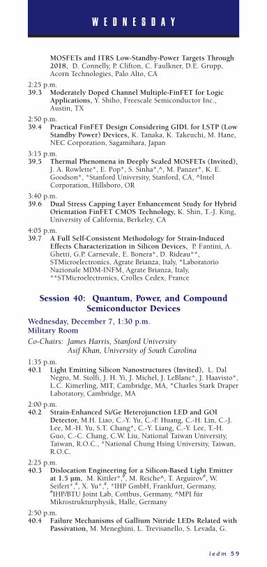
W E D N E S D A Y
MOSFETs and ITRS Low-Standby-Power Targets Through2018, D. Connelly, P. Clifton, C. Faulkner, D.E. Grupp,Acorn Technologies, Palo Alto, CA
2:25 p.m.39.3 Moderately Doped Channel Multiple-FinFET for Logic
Applications, Y. Shiho, Freescale Semiconductor Inc.,Austin, TX
2:50 p.m.39.4 Practical FinFET Design Considering GIDL for LSTP (Low
Standby Power) Devices, K. Tanaka, K. Takeuchi, M. Hane,NEC Corporation, Sagamihara, Japan
3:15 p.m.39.5 Thermal Phenomena in Deeply Scaled MOSFETs (Invited),
J. A. Rowlette*, E. Pop*, S. Sinha*,^, M. Panzer*, K. E.Goodson*, *Stanford University, Stanford, CA, ^IntelCorporation, Hillsboro, OR
3:40 p.m.39.6 Dual Stress Capping Layer Enhancement Study for Hybrid
Orientation FinFET CMOS Technology, K. Shin, T.-J. King,University of California, Berkeley, CA
4:05 p.m.39.7 A Full Self-Consistent Methodology for Strain-Induced
Effects Characterization in Silicon Devices, P. Fantini, A.Ghetti, G.P. Carnevale, E. Bonera*, D. Rideau**,STMicroelectronics, Agrate Brianza, Italy, *LaboratorioNazionale MDM-INFM, Agrate Brianza, Italy,**STMicroelectronics, Crolles Cedex, France
Session 40: Quantum, Power, and CompoundSemiconductor Devices
Wednesday, December 7, 1:30 p.m.Military RoomCo-Chairs: James Harris, Stanford University
Asif Khan, University of South Carolina
1:35 p.m.40.1 Light Emitting Silicon Nanostructures (Invited), L. Dal
Negro, M. Stolfi, J. H. Yi, J. Michel, J. LeBlanc*, J. Haavisto*,L.C. Kimerling, MIT, Cambridge, MA, *Charles Stark DraperLaboratory, Cambridge, MA
2:00 p.m.40.2 Strain-Enhanced Si/Ge Heterojunction LED and GOI
Detector, M.H. Liao, C.-Y. Yu, C.-F. Huang, C.-H. Lin, C.-J.Lee, M.-H. Yu, S.T. Chang*, C.-Y. Liang, C.-Y. Lee, T.-H.Guo, C.-C. Chang, C.W. Liu, National Taiwan University,Taiwan, R.O.C., *National Chung Hsing University, Taiwan,R.O.C.
2:25 p.m.40.3 Dislocation Engineering for a Silicon-Based Light Emitter
at 1.5 µm, M. Kittler*,#, M. Reiche^, T. Arguirov#, W.Seifert*,#, X. Yu*,#, *IHP GmbH, Frankfurt, Germany,#IHP/BTU Joint Lab, Cottbus, Germany, ^MPI fürMikrostrukturphysik, Halle, Germany
2:50 p.m.40.4 Failure Mechanisms of Gallium Nitride LEDs Related with
Passivation, M. Meneghini, L. Trevisanello, S. Levada, G.
i e d m 5 9
Jp 14-62 10/10/05 11:05 AM Page 59
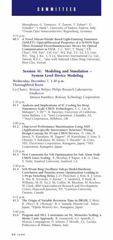
C O M M I T T E E S
6 0 i e d m
Meneghesso, G. Tamiazzo, E. Zanoni T. Zahner*, U.Zehnder*, V. Härle*, University of Padova, Padova, Italy,*Osram Opto Semiconductors, Regensburg, Germany
3:15 p.m.40.5 A Novel Silicon-Nitride Based Light-Emitting Transistor
(SiNLET): Optical/Electrical Properties of a SONOS-TypeThree-Terminal Electroluminescence Device for OpticalCommunication in ULSI, C.C. Yeh*, T. Wang*, Y.R.Chen*, F.M. Pan*, S.H. Gu*, W.J. Tsai, T.C. Lu, Y.Y. Liao,W.C. Ting, J. Ku, C-Y Lu, Macronix International Co. Ltd.,Taiwan, R.O.C., *also with National Chiao-Tung University,Hsin-Chu, Taiwan
Session 41: Modeling and Simulation – System Level Device Modeling
Wednesday, December 7, 1:30 p.m.Thoroughbred RoomCo-Chairs: Reinout Woltjer, Philips Research Laboratories
EindhovenTatsuya Kunikiyo, Renesas Technology Corporation
1:35 p.m.41.1 Analysis and Implications of IC Cooling for Deep
Nanometer Scale CMOS Technologies, S.-C. Lin, R.Mahajan*, V. De**, K. Banerjee, University of California,Santa Barbara, CA, *Intel Corporation, Chandler, AZ,**Intel Corporation, Hillsboro, OR
2:00 p.m.41.2 Chip-Level Performance Maximization Using ASIS
(Application-specific Interconnect Structure) WiringDesign Concept for 45 nm CMOS Devices, N. Oda, H.Imura, N. Kawahara, M. Tagami*, H. Kunishima, S. Sone, S.Ohnishi, Y. Kakuhara, M. Sekine, Y. Hayashi*, K. Ueno,NEC Electronics Corporation, Kanagawa, Japan, *NECCorporation, Kanagawa, Japan
2:25 p.m.41.3 New Constraint for Vth Optimization for Sub 32nm Node
CMOS Gates Scaling, E. Morifuji, P. Kapur, A.K.-A. Chao,Y. Nishi, Stanford University, Stanford, CA
2:50 p.m.41.4 SOI 90-nm Ring Oscillator Sub-ps Model-Hardware
Correlation and Parasitic-aware Optimization Leading to1.94-ps Switching Delay, J.-O. Plouchart, J. Kim, B. J. Gross,K. Wu, R. Trzcinski, V. Karam*, T. Sandwick, P. Hyde, R.Williams, M.-H. Na, J. Mc Cullen, M. Bhushan, M. Ketchen,W. Clark, IBM Semiconductor Research and DevelopmentCenter, Hopewell Junction, NY, *Carleton University,Ontario, Canada
3:15 p.m.41.5 The Origin of Variable Retention Time in DRAM, Y. Mori,
K. Ohyu*, K. Okonogi*, R.-I. Yamada, Hitachi Ltd., Tokyo,Japan, *Elpida Memory Inc., Kanagawa, Japan
3:40 p.m.41.6 Program and SILC Constraints on NC Memories Scaling: a
Monte Carlo Approach, R. Gusmeroli, A.S. Spinelli, C.Monzio Compagnoni, D. Ielmini, F. Morelli, A.L. Lacaita,Politecnico di Milano, Milano, Italy
Jp 14-62 10/10/05 11:05 AM Page 60
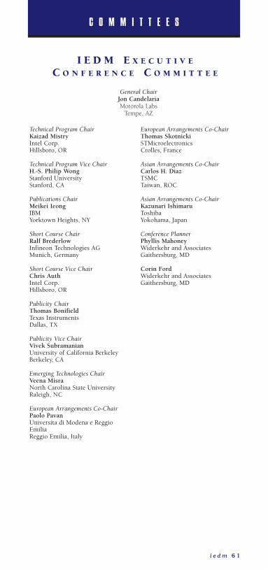
C O M M I T T E E S
I E D M E X E C U T I V EC O N F E R E N C E C O M M I T T E E
i e d m 6 1
Technical Program ChairKaizad MistryIntel Corp.Hillsboro, OR
Technical Program Vice ChairH.-S. Philip WongStanford UniversityStanford, CA
Publications ChairMeikei IeongIBMYorktown Heights, NY
Short Course ChairRalf BrederlowInfineon Technologies AGMunich, Germany
Short Course Vice ChairChris AuthIntel Corp.Hillsboro, OR
Publicity ChairThomas BonifieldTexas InstrumentsDallas, TX
Publicity Vice ChairVivek SubramanianUniversity of California BerkeleyBerkeley, CA
Emerging Technologies ChairVeena MisraNorth Carolina State UniversityRaleigh, NC
European Arrangements Co-ChairPaolo PavanUniversita di Modena e ReggioEmiliaReggio Emilia, Italy
European Arrangements Co-ChairThomas SkotnickiSTMicroelectronicsCrolles, France
Asian Arrangements Co-ChairCarlos H. DiazTSMCTaiwan, ROC
Asian Arrangements Co-ChairKazunari IshimaruToshibaYokohama, Japan
Conference PlannerPhyllis MahoneyWiderkehr and AssociatesGaithersburg, MD
Corin FordWiderkehr and AssociatesGaithersburg, MD
General ChairJon CandelariaMotorola Labs
Tempe, AZ
Jp 14-62 10/10/05 11:05 AM Page 61

C O M M I T T E E S
6 2 i e d m
C M O S D E V I C E SS U B C O M M I T T E E
Toshiro Hiramoto, ChairUniversity of TokyoTokyo, Japan
Serge BiesemansIMECLeuven, Belgium
Frederic BoeufSTMicroelectronicsCrolles, France
David BurnettFreescale SemiconductorAustin, TX
Kelin KuhnIntel CorporationHillsboro, OR
Robert LanderPhilips Research LeuvenLeuven, Belgium
Tatsuya OhguroToshiba CorporationYokohama, Japan
Huiling ShangIBM T. J. Watson Research CenterYorktown Heights, NY
Yuan TaurUniversity of California San DiegoLa Jolla, CA
Hitoshi WakabayashiNEC CorporationKanagawa, Japan
Howard C.-H. WangTSMCTaiwan, ROC
Qi XiangAMDSunnyvale, CA
Yee-Chia YeoNational University of SingaporeSingapore
C M O S A N D I N T E R C O N N E C TR E L I A B I L I T Y S U B C O M M I T T E E
Muhammad Ashraful Alam, ChairPurdue UniversityWest Lafayette, IN
Kaustav BanerjeeUniversity of California
Santa BarbaraSanta Barbara, CA
Koji EriguchiKyoto UniversityKyoto, Japan
Ben KaczerIMEC Leuven, Belgium
Seung KangAgere SystemsAllentown, PA
Charles LerouxCEA Grenoble, France
Ming-Fu LiNational University ofSingapore/Institute ofMicroelectronics SingaporeSingapore
Eiichi MurakamiRenesas Technology Corp.Ibaraki, Japan
Paul NicollianTexas Instruments Inc.Dallas, TX
Takeshi NogamiSony CorporationHopewell Junction, NY
William TontiIBM MicroelectronicsEssex Junction, VT
Angelo ViscontiSTMicroelectronicsAgrate Brianza, Italy
Jp 14-62 10/10/05 11:05 AM Page 62

C O M M I T T E E S
i e d m 6 3
D I S P L A Y S , S E N S O R S A N DM E M S S U B C O M M I T T E E
I N T E G R A T E D C I R C U I T S A N DM A N U F A C T U R I N GS U B C O M M I T T E E
Akintunde Akinwande, ChairMassachusetts Institute ofTechnologyCambridge, MA
Juergen BruggerEcole Polytechnique Federale
de Lausanne Lausanne, Switzerland
Kyuha ChungSamsung ElectronicsGyeonggi-Do, South Korea
Jo De BoeckIMECLeuven, Belgium
Homayoon HaddadAgilent TechnologiesCorvallis, OR
Amit LalCornell UniversityIthaca, NY
Keiji MabuchiSony CorporationKanagawa-ken, Japan
William MilneUniversity of CambridgeCambridge, United Kingdom
Arokia NathanUniversity of WaterlooWaterloo, Ontario, Canada
Roland ThewesInfineon TechnologiesMunich, Germany
Kazuya YonemotoMatsushita Electric
Industrial Co., Ltd.Kyoto, Japan
Darrin YoungCase Western Reserve UniversityCleveland, OH
Luan Tran, ChairMicron Technologies, Inc.Boise, ID
Roberto BezSTMicroelectronicsAgrate Brianza, Italy
Jean-Pierre ColingeUniversity of California DavisCarmichael, CA
Tahir GhaniIntelHillsboro, OR
Ted HoustonTexas InstrumentsDallas, TX
Shih-Fen HuangIBMHopewell Junction, NY
Takashi KobayashiHitachi, Ltd.Tokyo, Japan
Iwao KunishimaToshiba Corporation SemiconductorCompanyYokohama, Japan
Carlos MazureSOITECCrolles Cedex, France
Mike MendicinoMotorolaAustin, TX
Takashi NakabayashiMatsushita Electric Industrial Co.,Ltd.Kyoto, Japan
Yee Chaung SeeTSMCHsinchu, Taiwan
Sang-Pil SimSamsung ElectronicsKyeonggi-Do, Korea
Jp 14-62 10/10/05 11:05 AM Page 63
C O M M I T T E E S
6 4 i e d m
M O D E L I N G A N D S I M U L A T I O NS U B C O M M I T T E E
Conor Rafferty, ChairNoble Device TechnologiesNewark, NJ
Kuntal JoardarTexas InstrumentsTucson, AZ
Gerhard KlimeckPurdue UniversityWest Lafayette, IN
Jeong-Taek KongSamsung Electronics Co., Ltd.Gyeonggi-Do, Korea
Tatsuya KunikiyoRenesas Technology Corp.Hyogo, Japan
Juergen LorenzFraunhofer IISBErlangen, Germany
Mitiko Miura-MattauschHiroshima UniversityHigashi-Hiroshima, Japan
Enrico SangiorgiUniversity of BolognaForli, Italy
Martin StadeleInfineon Technologies AGMunich, Germany
Mark StettlerIntel CorporationHillsboro, OR
Reinout WoltjerPhilips Research LaboratoriesEindhovenEindhoven, The Netherlands
P R O C E S S T E C H N O L O G YS U B C O M M I T T E E
Glen Wilk, ChairASM AmericaPhoenix, AZ
Franck ArnaudSTMicroelectronicsCrolles, France
Gerald BeyerIMECLeuven, Belgium
S.C. ChenTSMCTaiwan, ROC
Simon DeleonibusCEA/LETIGrenoble Cedex, France
Martin GutscheInfineon TechnologiesMunich, Germany
Gyo Young JinSamsung ElectronicsYongin-Si, Gyeonggi-Do, Korea
Mehmet OzturkNorth Carolina State UniversityRaleigh, NC
Kyoichi SuguroToshiba Corp.Yokohama, Japan
Sunit TyagiIntelHillsboro, OR
Victor WangFreescale SemiconductorCrolles Cedex, France
Hirohito WatanabeNEC CorporationKanagawa, Japan
Min YangIBM, TJ Watson Research CenterYorktown Heights, NY
Jp 14-62 10/10/05 11:05 AM Page 64
C O M M I T T E E S
i e d m 6 5
Q U A N T U M P O W E R A N DC O M P O U N D S E M I C O N D U C T O R
D E V I C E S S U B C O M M I T T E E
Gaudenzio Meneghesso, ChairUniversity of PadovaPadova, Italy
Helmut BrechFreescale SemiconductorPhoenix, AZ
David ChowHRL LaboratoriesMalibu, CA
Jesus Del AlamoMassachusetts Institute ofTechnologyCambridge, MA
James HarrisStanford UniversityStanford, CA
Hideki HasegawaHokkaido UniversitySapporo, Japan
Yutaka HoshinoRenesas Technology Corp.Tokyo, Japan
Asif KahnUniversity of South CarolinaColumbia, SC
Ruediger QuayFraunhofer Institute of Applied
Solid-State PhysicsFreiburg, Germany
Dimitris PavlidisTechnische Universitat DarmstadtDarmstadt, Germany
Tetsuya SuemitsuNTT Photonics LaboratoriesKanagawa, Japan
Giovanni VerzellesiUniversita' di Modena e ReggioEmiliaModena, Italy
Joachim WuerflFerdinand-Braun-Institute Berlin, Germany
Mohammed ZaknouneC.N.R.S. IEMNVilleneuve d'Ascq Cedex, France
S O L I D S T A T E A N DN A N O E L E C T R O N I C D E V I C E S
S U B C O M M I T T E E
Bruce White, ChairFreescale SemiconductorAustin, TX
Klaus AufingerInfineon Technologies AGMunich, Germany
Jean-Luc AutranUniversite MarseilleMarseille Cedex 13, France
M. Jamal DeenMcMaster UniversityHamilton, Ontario, Canada
Ali JaveyStanford UniversityStanford, CA
Ted KaminsHewlett-PackardPalo Alto, CA
Yukihiro KiyotaSony CorporationKanagawa, Japan
Zoran KrivokapicAMDSunnyvale, CA
Mark ReedYale UniversityNew Haven, CT
Ken UchidaToshiba Corp.Yokohama, Japan
Frans P. WiddershovenPhilips Research LeuvenLeuven, Belgium
Kanji YohHokkaido UniversitySapporo, Japan
Jp 14-62 10/10/05 11:05 AM Page 65

N O T E S
6 6 i e d m
Jp 14-62 10/10/05 11:05 AM Page 66

N O T E S
i e d m 6 7
Jp 14-62 10/10/05 11:05 AM Page 67

N O T E S
6 8 i e d m
Jp 14-62 10/10/05 11:05 AM Page 68

2005
Hilton Washingtonand TowersWashington, DCDecember 5-7, 2005
Sponsored by Electron Devices Society of IEEE
iedmiedm�
iedmiedm2 0 0 5 C o n f e r e n c ea t a G l a n c e
international Electron Devices meetinginternational Electron Devices meeting
Pres
orted
First
Clas
s Mail
U.S.
Pos
tage
PAID
Rock
ville,
MD
Perm
it No
. 800
1622
0 S.
Fre
deric
k Av
enue
Suite
312
Gaith
ersb
urg,
MD
208
77US
A Adva
nce
Prog
ram
Dec
embe
r 5-
7, 2
005
see
our
hom
e pa
geht
tp://
ww
w.i
eee.
org/
conf
eren
ce/ie
dm
inte
rnat
iona
l Ele
ctro
n D
evic
es m
eetin
gie
dmie
dm20
05
Jp Cover Spreads 10/6/05 12:37 PM Page 1