Journal of Materials Chemistry C -...
7
3616 | J. Mater. Chem. C, 2017, 5, 3616--3622 This journal is © The Royal Society of Chemistry 2017 Cite this: J. Mater. Chem. C, 2017, 5, 3616 Effect of alkyl chain spacer on charge transport in n-type dominant polymer semiconductors with a diketopyrrolopyrrole-thiophene-bithiazole acceptor–donor–acceptor unit† Hojeong Yu,‡ ab Hyong Nam Kim,‡ c Inho Song, a Yeon Hee Ha, c Hyungju Ahn, d Joon Hak Oh * a and Yun-Hi Kim * c Although the effects of alkyl chain spacers have been extensively studied for p-type conjugated polymers with a donor (D)–acceptor (A) repeating unit, few studies have examined their effects for n-type polymers with an A–D–A architecture having two different acceptors in the repeating unit. Herein, diketopyrrolopyrrole-thiophene-bithiazole A–D–A type polymer semiconductors (DPPBTz) con- taining branched alkyl chains of 24-alkyl with C1 spacer (P-24-DPPBTz) and 29-alkyl with C6 spacer (P-29-DPPBTz) were designed and synthesized to elucidate the effect of the alkyl chain branching position on the electron-dominant charge transport system. Due to the strong electron deficiency and trans-planar conformation of the bithiazole group, DPPBTz-based polymer semiconductors exhibit n-type dominant electrical properties with a high electron mobility of up to 1.87 cm 2 V 1 s 1 . Systematic studies on the photophysical properties, thin-film microstructures, and electrical properties of the DPPBTz polymers revealed that upon modification of the branching position, A–D–A n-type dominant semiconductors differently behave compared to D–A p-type dominant semiconductors. This is attributed to the relatively weaker intermolecular interactions in A–D–A type semiconductors, making the C1 spacer more efficient for electron transport. These findings reveal the molecular design rule of alkyl side-chains in A–D–A n-type-dominant conjugated polymers for the first time. Introduction Polymeric semiconductors for organic field-effect transistors (OFETs) have been extensively studied as structural modifications and solution processability can be easily performed and device fabrication is relatively inexpensive. 1,2 Recently, great advances in polymeric semiconductors have been made through molecular design and device optimization. 3–14 A number of polymers exhibit high carrier mobility, exceeding 0.1 cm 2 V 1 s 1 , comparable to that of amorphous silicon. Especially, donor(D)–acceptor(A)-type copolymers containing diketopyrrolopyrrole (DPP) and isoindigo- based copolymers have attracted significant interest for promising applications in OFETs. 5–7,12–17 Optimization of the molecular structure is one of the most effective ways to achieve a high carrier mobility. It has been reported that charge transport in organic semiconductors not only involves intramolecular transport, but also intermolecular and interdomain transport. 3 Various D–A polymers have been designed to obtain a p-planar backbone, which enables high crystallinity in thin films. In general, p-conjugated backbone structures critically affect the coplanarity, solubility, molecular weight, energy level, and molecular packing of the polymers. Long-branched alkyl side chains are highly beneficial for improving the solubility of the polymers; however, as insulators, they tend to degrade the charge transport, and their bulkiness inhibits intermolecular interactions. Recent studies, including work from our research groups, have demonstrated that control over the branching position of the linear spaced-alkyl chains can result in a dramatic increase in the charge carrier mobilities of p-type and p-type-dominant ambipolar polymers. 7,12,18–21 Tuning the alkyl spacer length between the branching point and the backbone from C1 to C6 in DPP-based highly p-extended a Department of Chemical Engineering, Pohang University of Science and Technology (POSTECH), Pohang, Gyeongbuk 790-784, South Korea. E-mail: [email protected] b School of Energy and Chemical Engineering, Ulsan National Institute of Science and Technology (UNIST), Ulsan 689-798, South Korea c Department of Chemistry and RIGET, Gyeongsang National University, 900, Gajwa-dong, Jinju, Gyeongnam, 660-701, South Korea. E-mail: [email protected] d Pohang Accelerator Laboratory, Pohang University of Science and Technology (POSTECH), Pohang, Gyeongbuk 790-784, South Korea † Electronic supplementary information (ESI) available: Synthetic details and characterization data, additional figures (cyclic voltammetry plots, additional XRD analysis data, AFM phase images), FET fabrication and testing. See DOI: 10.1039/c7tc00044h ‡ These authors contributed equally to this work. Received 5th January 2017, Accepted 13th March 2017 DOI: 10.1039/c7tc00044h rsc.li/materials-c Journal of Materials Chemistry C PAPER Published on 14 March 2017. Downloaded by POSTECH Library on 02/06/2017 08:48:00. View Article Online View Journal | View Issue
Transcript of Journal of Materials Chemistry C -...

3616 | J. Mater. Chem. C, 2017, 5, 3616--3622 This journal is©The Royal Society of Chemistry 2017
Cite this: J.Mater. Chem. C, 2017,
5, 3616
Effect of alkyl chain spacer on charge transport inn-type dominant polymer semiconductors with adiketopyrrolopyrrole-thiophene-bithiazoleacceptor–donor–acceptor unit†
Hojeong Yu,‡ab Hyong Nam Kim,‡c Inho Song,a Yeon Hee Ha,c Hyungju Ahn,d
Joon Hak Oh *a and Yun-Hi Kim *c
Although the effects of alkyl chain spacers have been extensively studied for p-type conjugated
polymers with a donor (D)–acceptor (A) repeating unit, few studies have examined their effects for
n-type polymers with an A–D–A architecture having two different acceptors in the repeating unit.
Herein, diketopyrrolopyrrole-thiophene-bithiazole A–D–A type polymer semiconductors (DPPBTz) con-
taining branched alkyl chains of 24-alkyl with C1 spacer (P-24-DPPBTz) and 29-alkyl with C6 spacer
(P-29-DPPBTz) were designed and synthesized to elucidate the effect of the alkyl chain branching
position on the electron-dominant charge transport system. Due to the strong electron deficiency and
trans-planar conformation of the bithiazole group, DPPBTz-based polymer semiconductors exhibit
n-type dominant electrical properties with a high electron mobility of up to 1.87 cm2 V�1 s�1. Systematic
studies on the photophysical properties, thin-film microstructures, and electrical properties of the
DPPBTz polymers revealed that upon modification of the branching position, A–D–A n-type dominant
semiconductors differently behave compared to D–A p-type dominant semiconductors. This is
attributed to the relatively weaker intermolecular interactions in A–D–A type semiconductors, making
the C1 spacer more efficient for electron transport. These findings reveal the molecular design rule of
alkyl side-chains in A–D–A n-type-dominant conjugated polymers for the first time.
Introduction
Polymeric semiconductors for organic field-effect transistors(OFETs) have been extensively studied as structural modificationsand solution processability can be easily performed and devicefabrication is relatively inexpensive.1,2 Recently, great advances inpolymeric semiconductors have been made through moleculardesign and device optimization.3–14 A number of polymers exhibithigh carrier mobility, exceeding 0.1 cm2 V�1 s�1, comparable to
that of amorphous silicon. Especially, donor(D)–acceptor(A)-typecopolymers containing diketopyrrolopyrrole (DPP) and isoindigo-based copolymers have attracted significant interest for promisingapplications in OFETs.5–7,12–17 Optimization of the molecularstructure is one of the most effective ways to achieve a highcarrier mobility. It has been reported that charge transport inorganic semiconductors not only involves intramolecular transport,but also intermolecular and interdomain transport.3 Various D–Apolymers have been designed to obtain a p-planar backbone, whichenables high crystallinity in thin films. In general, p-conjugatedbackbone structures critically affect the coplanarity, solubility,molecular weight, energy level, and molecular packing of thepolymers. Long-branched alkyl side chains are highly beneficialfor improving the solubility of the polymers; however, as insulators,they tend to degrade the charge transport, and their bulkinessinhibits intermolecular interactions. Recent studies, includingwork from our research groups, have demonstrated that controlover the branching position of the linear spaced-alkyl chains canresult in a dramatic increase in the charge carrier mobilities ofp-type and p-type-dominant ambipolar polymers.7,12,18–21
Tuning the alkyl spacer length between the branching pointand the backbone from C1 to C6 in DPP-based highly p-extended
a Department of Chemical Engineering, Pohang University of Science and
Technology (POSTECH), Pohang, Gyeongbuk 790-784, South Korea.
E-mail: [email protected] School of Energy and Chemical Engineering, Ulsan National Institute of Science
and Technology (UNIST), Ulsan 689-798, South Koreac Department of Chemistry and RIGET, Gyeongsang National University, 900,
Gajwa-dong, Jinju, Gyeongnam, 660-701, South Korea. E-mail: [email protected] Pohang Accelerator Laboratory, Pohang University of Science and Technology
(POSTECH), Pohang, Gyeongbuk 790-784, South Korea
† Electronic supplementary information (ESI) available: Synthetic details andcharacterization data, additional figures (cyclic voltammetry plots, additionalXRD analysis data, AFM phase images), FET fabrication and testing. See DOI:10.1039/c7tc00044h‡ These authors contributed equally to this work.
Received 5th January 2017,Accepted 13th March 2017
DOI: 10.1039/c7tc00044h
rsc.li/materials-c
Journal ofMaterials Chemistry C
PAPER
Publ
ishe
d on
14
Mar
ch 2
017.
Dow
nloa
ded
by P
OST
EC
H L
ibra
ry o
n 02
/06/
2017
08:
48:0
0.
View Article OnlineView Journal | View Issue

This journal is©The Royal Society of Chemistry 2017 J. Mater. Chem. C, 2017, 5, 3616--3622 | 3617
p-type polymers causes the maximum hole mobility to increaseby as much as 17.8 cm2 V�1 s�1.10,22 The dramatic change in thecharge transport properties via side-chain engineering can beachieved because the side chains induce backbone planaritysuch that to reduce steric hindrance, and this increases crystal-linity due to long-range ordering. The side chain also affects thechain packing density, and mobility depends on the odd–evennumber of linear alkyl spacers.22,23 Although many systematicstudies for p-type and ambipolar semiconducting polymershave been carried out, studies on n-type dominant polymersare relatively rare.
Recently, one of our groups reported a dramatic polaritychange in an n-type material by introducing a cyano group on awell-known p-type DPP-TVT polymer and as a result, DPP-CNTVT was obtained.14 Reichmanis et al. reported that poly-(dithienyldiketopyrrolopyrrolebithiazole), which is composedof DPP containing alkyl side chains of 27 carbons with a linearspacer of 4 carbons and bithiazole, exhibits an electron mobilityapproaching 0.3 cm2 V�1 s�1.24 The introduction of electron-deficient bithiazole units with transplanar conformationinduced n-type characteristics in a low work-function electrodeand passivating dielectric system. In addition, to minimize stericeffects within the DPPBTz backbone, 5-decylheptadecyl sidechains were introduced. The 27-carbon alkyl with 4-carbon linearspacers not only increased solubility in an eco-friendly solvent,but also promoted p–p interchain interactions.24
In this study, we designed two polymers, P-24-DPPBTz andP-29-DPPBTz, which are composed of two electron-acceptingunits, bithiazole and DPP, and contain 24-carbon alkyl chainswith a 1-carbon linear spacer (C1) and 29-carbon alkyl chainswith a 6-carbon linear spacer (C6), respectively. Although theeffect of the alkyl chain on the dramatic increase in chargecarrier mobility in p-type polymers has been extensively andsystematically studied by adjusting the branching position, fewstudies have examined the development of n-type semiconduc-tors, particularly polymers with an A–D–A architecture, whichhave two different acceptors in the repeating unit. Thus, to thebest of our knowledge, this is the first report on the effect of thealkyl side chain on n-type-dominant semiconducting polymers.
Results and discussionSynthesis and characterization
Synthesis of P-24-DPPBTz and P-29-DPPBTz was carried outvia the Stille coupling reaction using Pd2(dba)3 and P(oTol)3
for 48 h in chlorobenzene (Fig. 1). The synthesis details areprovided in the ESI† (Fig. S1). The crude polymers were purifiedby precipitation from methanol, followed by successive Soxhletextractions. The polymers had good solubility in commonorganic solvents such as tetrahydrofuran, chloroform, andchlorobenzene. Gel-permeation chromatography (GPC) analysisrevealed a number average molecular weight (Mn) of 56 kg mol�1
for P-24-DPPBTz and 64 kg mol�1 for P-29-DPPBTz, with poly-dispersities of 1.55 and 1.78, respectively.
The absorption spectra of P-24-DPPBTz and P-29-DPPBTzwere obtained in chloroform solution. Both polymers showed adistinct dual band absorption (Fig. 2). P-29-DPPBTz showed amarked red-shifted absorption in solution as a planar back-bone was formed such that to reduce steric hindrance byplacing branching points away. This result was similar to thatobtained for p-type polymers.10,22 Both the as-prepared andannealed polymer films showed slightly red-shifted and verybroad absorption peaks compared with those in solution. Theoptical band gaps of the polymers (1.35 eV and 1.29 eV) werecalculated from the absorption edge of 916 nm for P-24-DPPBTzand 954 nm for P-29-DPPBTz, respectively (Table 1). Cyclic voltam-metry (CV) measurements were performed to determine the elec-tronic energy structure of both polymers. The highest occupiedmolecular orbital (HOMO) levels of P-24-DPPBTz and P-29-DPPBTzwere �5.31 eV and �5.35 eV, respectively, and the lowest unoccu-pied molecular orbital (LUMO) levels were �3.96 eV and �4.06 eV,respectively. The low-lying LUMO levels of P-24-DPPBTz andP-29-DPPBTz provided a high potential for good ambient stabilityin electron transport organic semiconductors (Fig. S2, ESI†).
Both P-24-DPPBTz and P-29-DPPBTz showed good thermalstability, with the decomposition temperatures above 420 1C.There was no evidence of phase transitions for either polymerin differential scanning calorimetry (DSC) measurements(Fig. S3, ESI†).
Fig. 1 Schematic for the synthesis of P-24-DPPBTz and P-29-DPPBTz.
Paper Journal of Materials Chemistry C
Publ
ishe
d on
14
Mar
ch 2
017.
Dow
nloa
ded
by P
OST
EC
H L
ibra
ry o
n 02
/06/
2017
08:
48:0
0.
View Article Online
3618 | J. Mater. Chem. C, 2017, 5, 3616--3622 This journal is©The Royal Society of Chemistry 2017
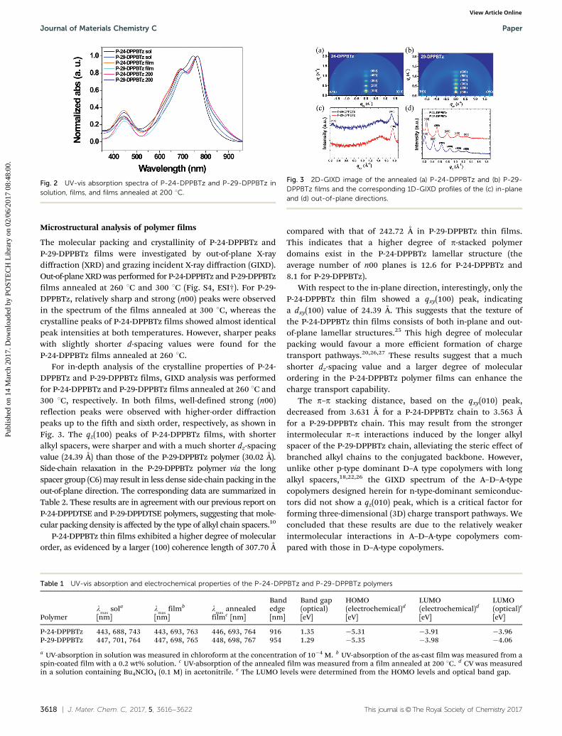
Microstructural analysis of polymer films
The molecular packing and crystallinity of P-24-DPPBTz andP-29-DPPBTz films were investigated by out-of-plane X-raydiffraction (XRD) and grazing incident X-ray diffraction (GIXD).Out-of-plane XRD was performed for P-24-DPPBTz and P-29-DPPBTzfilms annealed at 260 1C and 300 1C (Fig. S4, ESI†). For P-29-DPPBTz, relatively sharp and strong (n00) peaks were observedin the spectrum of the films annealed at 300 1C, whereas thecrystalline peaks of P-24-DPPBTz films showed almost identicalpeak intensities at both temperatures. However, sharper peakswith slightly shorter d-spacing values were found for theP-24-DPPBTz films annealed at 260 1C.
For in-depth analysis of the crystalline properties of P-24-DPPBTz and P-29-DPPBTz films, GIXD analysis was performedfor P-24-DPPBTz and P-29-DPPBTz films annealed at 260 1C and300 1C, respectively. In both films, well-defined strong (n00)reflection peaks were observed with higher-order diffractionpeaks up to the fifth and sixth order, respectively, as shown inFig. 3. The qz(100) peaks of P-24-DPPBTz films, with shorteralkyl spacers, were sharper and with a much shorter dz-spacingvalue (24.39 Å) than those of the P-29-DPPBTz polymer (30.02 Å).Side-chain relaxation in the P-29-DPPBTz polymer via the longspacer group (C6) may result in less dense side-chain packing in theout-of-plane direction. The corresponding data are summarized inTable 2. These results are in agreement with our previous report onP-24-DPPDTSE and P-29-DPPDTSE polymers, suggesting that mole-cular packing density is affected by the type of alkyl chain spacers.10
P-24-DPPBTz thin films exhibited a higher degree of molecularorder, as evidenced by a larger (100) coherence length of 307.70 Å
compared with that of 242.72 Å in P-29-DPPBTz thin films.This indicates that a higher degree of p-stacked polymerdomains exist in the P-24-DPPBTz lamellar structure (theaverage number of n00 planes is 12.6 for P-24-DPPBTz and8.1 for P-29-DPPBTz).
With respect to the in-plane direction, interestingly, only theP-24-DPPBTz thin film showed a qxy(100) peak, indicatinga dxy(100) value of 24.39 Å. This suggests that the texture ofthe P-24-DPPBTz thin films consists of both in-plane and out-of-plane lamellar structures.25 This high degree of molecularpacking would favour a more efficient formation of chargetransport pathways.20,26,27 These results suggest that a muchshorter dz-spacing value and a larger degree of molecularordering in the P-24-DPPBTz polymer films can enhance thecharge transport capability.
The p–p stacking distance, based on the qxy(010) peak,decreased from 3.631 Å for a P-24-DPPBTz chain to 3.563 Åfor a P-29-DPPBTz chain. This may result from the strongerintermolecular p–p interactions induced by the longer alkylspacer of the P-29-DPPBTz chain, alleviating the steric effect ofbranched alkyl chains to the conjugated backbone. However,unlike other p-type dominant D–A type copolymers with longalkyl spacers,18,22,26 the GIXD spectrum of the A–D–A-typecopolymers designed herein for n-type-dominant semiconduc-tors did not show a qz(010) peak, which is a critical factor forforming three-dimensional (3D) charge transport pathways. Weconcluded that these results are due to the relatively weakerintermolecular interactions in A–D–A-type copolymers com-pared with those in D–A-type copolymers.
Fig. 2 UV-vis absorption spectra of P-24-DPPBTz and P-29-DPPBTz insolution, films, and films annealed at 200 1C.
Table 1 UV-vis absorption and electrochemical properties of the P-24-DPPBTz and P-29-DPPBTz polymers
Polymerl
maxsola
[nm]l
maxfilmb
[nm]l
maxannealed
filmc [nm]
Bandedge[nm]
Band gap(optical)[eV]
HOMO(electrochemical)d
[eV]
LUMO(electrochemical)d
[eV]
LUMO(optical)e
[eV]
P-24-DPPBTz 443, 688, 743 443, 693, 763 446, 693, 764 916 1.35 �5.31 �3.91 �3.96P-29-DPPBTz 447, 701, 764 447, 698, 765 448, 698, 767 954 1.29 �5.35 �3.98 �4.06
a UV-absorption in solution was measured in chloroform at the concentration of 10�4 M. b UV-absorption of the as-cast film was measured from aspin-coated film with a 0.2 wt% solution. c UV-absorption of the annealed film was measured from a film annealed at 200 1C. d CV was measuredin a solution containing Bu4NClO4 (0.1 M) in acetonitrile. e The LUMO levels were determined from the HOMO levels and optical band gap.
Fig. 3 2D-GIXD image of the annealed (a) P-24-DPPBTz and (b) P-29-DPPBTz films and the corresponding 1D-GIXD profiles of the (c) in-planeand (d) out-of-plane directions.
Journal of Materials Chemistry C Paper
Publ
ishe
d on
14
Mar
ch 2
017.
Dow
nloa
ded
by P
OST
EC
H L
ibra
ry o
n 02
/06/
2017
08:
48:0
0.
View Article Online

This journal is©The Royal Society of Chemistry 2017 J. Mater. Chem. C, 2017, 5, 3616--3622 | 3619
To elucidate the molecular packing characteristics in termsof morphological aspects, we investigated the morphologies ofthe P-24-DPPBTz and P-29-DPPBTz polymer films (annealed attheir respective optimized temperatures) by tapping-modeatomic force microscopy (AFM). Fig. 4 shows the AFM heightimages (3 � 3 mm scan) of the P-24-DPPBTz and P-29-DPPBTzpolymer films. The corresponding phase images are presented inFig. S2 (ESI†). The P-29-DPPBTz polymer films were composed ofnanoscale fibrillar domains with a good intergrain connectivity.Remarkably, however, the P-24-DPPBTz films exhibited largeaggregates of fibrils with the formation of voids in a multiple-layer structure, which indicates a rough surface coverage.28
Fabrication of solution-processed FETs and I–Vcharacterizations
To investigate the charge transport properties of P-24-DPPBTzand P-29-DPPBTz polymer films, bottom-gate top-contactFETs were fabricated. The polymer solutions were prepared inchlorobenzene at the concentration of 2 mg mL�1. The filmswere deposited on a n-octadecyltrimethoxysilane (OTS)-modifiedSiO2/Si substrate by spin-coating and drop-casting methods. Theexperimental details are included in the Experimental section.The P-24-DPPBTz and P-29-DPPBTz FETs exhibited electron-dominant ambipolar transport, most likely due to the energeti-cally low-lying LUMO levels promoted by the bithiazole groupand the lower injection barriers for electrons with regard to goldelectrodes (work function: B5.1 eV). The electrical performances
of the FETs based on P-24-DPPBTz and P-29-DPPBTz polymerfilms are listed in Table 3. The bithiazole group in the polymerbackbone strengthen the electron charge-carrier transportin the FETs and is expected to afford n-channel dominantambipolar OFETs, in line with our aforementioned hypothesis.To explore the optimized heat treatment conditions with highthermal stability considerations, 23 spin-coated and drop-castpolymer thin films were annealed at 220 1C, 260 1C, and 300 1Cfor 30 min.
Fig. S3 (ESI†) shows the average field-effect mobility varia-tions of P-24-DPPBTz and P-29-DPPBTz FETs with standarddeviation values at various annealing temperatures. The optimalfilms were obtained by the drop-casting method. The bestperformances were achieved by applying a heat treatment ofup to 260 1C and 300 1C for P-24-DPPBTz and P-29-DPPBTz,respectively. The typical transfer and output curves of optimizedFETs based on the P-24-DPPBTz and P-29-DPPBTz films areshown in Fig. 5. In both FETs based on P-24-DPPBTz andP-29-DPPBTz, n-channel dominant ambipolar characteristicswere observed. According to the FET mobility results, FETs basedon P-24-DPPBTz mostly exhibited a higher performance in bothelectron and hole transport than FETs based on P-29-DPPBTz,exhibiting remarkably high maximum (average) me and mh valuesof 1.87 and 0.30 (1.49 and 0.15, respectively) cm2 V�1 s�1 at260 1C, respectively (Table 3). Maximum and average electronmobilities of 0.89 and 0.77 cm2 V�1 s�1, respectively, wereobtained from the optimized P-29-DPPBTz films (annealedat 300 1C), whereas the hole mobilities were approximately0.1 cm2 V�1 s�1 under several annealing conditions. Thesefindings indicate that charge transport in these polymerscontaining a bithiazole group is more significantly affectedby the molecular packing orientation and density than themorphological features.
More importantly, note that in our bithiazole-based polymerbackbone system, a shorter alkyl spacer (C1) was more efficientto enhance electron transport rather than a long alkyl spacer(C6). This result is contrary to that obtained in our previousreport on DPP-SVS and DPP-TVT polymer series that containselenophene–vinylene–selenophene and thiophene–vinylene–thiophene units, respectively; herein, the optimized alkyl chainspacer unit was C6.7,22,23 Other than this exception, the longer
Table 2 Crystallographic parameters calculated from the GIXD diffractogram profiles of the optimized P-24-DPPBTz and P-29-DPPBTz thin films
Crystallographic parametersa 24-DPPBTz 29-DPPBTz
From qz
profile (100) lamellar spacing q (�1
) 0.2576 0.2093d-Spacing (Å) 24.39 30.02Coherence length (Å) 307.70 242.72Avg. # of h00 plane (N) 12.6 8.1
From qxy
profile (100) lamellar spacing q (�1
) 0.2614 N/Ab
d-Spacing (Å) 24.04 N/Ab
(010) p–p stack q (Å�1
) 1.7304 1.7632d-Spacing (Å) 3.63 3.56
a Polymer films were prepared by drop-casting and thermal treatment at the optimized temperature (260 1C and 300 1C for P-24-DPPBTz andP-29-DPPBTz, respectively), and their parameters were calculated from the GIXD profiles. b For 29-DPPBTz films, the (100) lamellar peak was notobserved in the in-plane GIXD patterns.
Fig. 4 AFM height images of the (a) P-24-DPPBTz and (b) P-29-DPPBTzfilms annealed at 260 1C and 300 1C, respectively.
Paper Journal of Materials Chemistry C
Publ
ishe
d on
14
Mar
ch 2
017.
Dow
nloa
ded
by P
OST
EC
H L
ibra
ry o
n 02
/06/
2017
08:
48:0
0.
View Article Online

3620 | J. Mater. Chem. C, 2017, 5, 3616--3622 This journal is©The Royal Society of Chemistry 2017
d-spacings in P-29-DPP-SVS showed two- to three-fold higherhole mobility than those in P-24-DPP-SVS, due to its edge-ondominant molecular orientation.7
Intriguingly, DPPBTz polymers with a smaller alkyl spacershowed better electrical performance both in p-channel andn-channel operations. In DPPBTz polymers, which have anA–D–A architecture, P-24-DPPBTz showed higher hole andelectron mobility. As described above, the XRD spectrumof the A–D–A-type copolymers designed for n-type-dominant
semiconductors did not show a qz(010) peak, which is a criticalfactor for forming 3D charge transport pathways. This couldpresumably be due to the relatively weaker intermolecularinteractions in A–D–A-type copolymers compared with thosein D–A-type copolymers. In A–D–A architecture, the inter-molecular interactions may become weaker due to therelatively poor donor moiety, which can disturb the formationof a bimodal molecular packing, unlike in p-type-dominantD–A systems.
Table 3 OFET performance of P-24-DPPBTz and P-29-DPPBTz films
Polymer FilmsThermalannealing (1C)
p-Channela n-Channelb
mh,maxc
[cm2 V�1 s�1]mh,avg
d
[cm2 V�1 s�1] Ion/Ioff
me,maxc
[cm2 V�1 s�1]me,avg
d
[cm2 V�1 s�1] Ion/Ioff
P-24-DPPBTz Spin-coated As-cast 0.054 0.039 (�0.0092)e 4103 0.59 0.45 (�0.12)e 4103
220 0.12 0.089 (�0.024) 4104 0.99 0.65 (�0.28) 4104
260 0.17 0.10 (�0.040) 4103 1.53 0.96 (�0.46) 4104
300 0.072 0.051 (�0.012) 4103 1.08 0.71 (�0.28) 4103
Drop-cast As-cast 0.081 0.052 (�0.019) 4104 0.59 0.32 (�0.12) 4105
220 0.15 0.13 (�0.018) 4104 1.05 0.72 (�0.23) 4104
260 0.3 0.15 (�0.071) 4104 1.87 1.49 (�0.32) 4106
300 0.14 0.086 (�0.036) 4104 1.23 0.87 (�0.27) 4104
P-29-DPPBTz Spin-coated As-cast 0.065 0.048 (�0.015) 4104 0.26 0.23 (�0.020) 4104
220 0.063 0.051 (�0.013) 4105 0.34 0.26 (�0.053) 4104
260 0.11 0.078 (�0.023) 4105 0.33 0.20 (�0.11) 4105
300 0.16 0.076 (�0.035) 4105 0.38 0.34 (�0.025) 4106
Drop-cast As-cast 0.057 0.045 (�0.012) 4104 0.33 0.30 (�0.016) 4105
220 0.088 0.053 (�0.021) 4104 0.39 0.30 (�0.061) 4104
260 0.13 0.077 (�0.022) 4105 0.58 0.45 (�0.053) 4105
300 0.09 0.066 (�0.023) 4104 0.89 0.77 (�0.10) 4103
a The p-channel characteristics of P-24-DPPBTz measured at VDS = �100 V. b n-Channel characteristics of P-29-DPPBTz-FETs measured atVDS = 100 V. c Maximum mobility over 10 FET devices with a channel length (L) of B50 mm and a channel width (W) of B1000 mm. d Averagemobility over 10 FET devices with a channel length (L) of B50 mm and a channel width (W) of B1000 mm. e Standard deviation.
Fig. 5 FET characteristics of P-24-DPPBTz and P-29-DPPBTz films annealed at 260 1C and 300 1C, respectively. Transfer curves of P-24-DPPBTz andP-29-DPPBTz at (a and e) hole- and (b and f) electron-enhancement operation at VDS = �100 and +100 V, respectively. Output curves of P-24-DPPBTzand P-29-DPPBTz films at (c and g) p- and (d and h) n-channel operation, respectively.
Journal of Materials Chemistry C Paper
Publ
ishe
d on
14
Mar
ch 2
017.
Dow
nloa
ded
by P
OST
EC
H L
ibra
ry o
n 02
/06/
2017
08:
48:0
0.
View Article Online
This journal is©The Royal Society of Chemistry 2017 J. Mater. Chem. C, 2017, 5, 3616--3622 | 3621
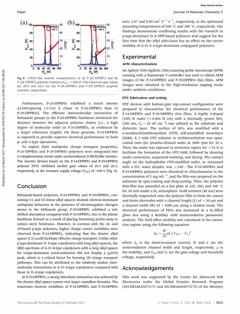
Furthermore, P-24-DPPBTz exhibited a much shorterdz(100)-spacing (E5.63 Å closer in P-24-DPPBTz than inP-29-DPPBTz). The efficient intermolecular interaction ofbithiazole groups in the P-24-DPPBTz backbone shortened thedistance between the adjacent polymer chains (i.e., a highdegree of molecular order in P-24-DPPBTz, as evidenced bya larger coherence length). On these grounds, P-24-DPPBTzis expected to provide superior electrical performance in bothp- and n-type operations.
To exploit their ambipolar charge transport properties,P-24-DPPBTz and P-29-DPPBTz polymers were integrated intoa complementary metal–oxide–semiconductor (CMOS)-like inverter.The inverter devices based on the P-24-DPPBTz and P-29-DPPBTzpolymer FETs exhibited similar gain values of 29.3 and 26.3,respectively, at the constant supply voltage (VDD) of +100 V (Fig. 6).
Conclusion
Bithiazole-based polymers, P-24-DPPBTz and P-29-DPPBTz, con-taining C1 and C6 linear alkyl spacers showed electron-dominantambipolar behaviors in the presence of electronegative nitrogenatoms in the bithiazole group. P-29-DPPBTz exhibited a red-shifted absorption compared with P-24-DPPBTz, due to the planarbackbone formed as a result of placing branching points away toreduce steric hindrance. However, in contrast with the 24- and29-based p-type polymers, higher charge carrier mobilities wereobserved from P-24-DPPBTz, indicating that the shorter alkylspacer (C1) could facilitate effective charge transport. Unlike otherp-type-dominant D–A-type copolymers with long alkyl spacers, theXRD spectrum of A–D–A-type copolymers with a long alkyl spacerfor n-type-dominant semiconductors did not display a qz(010)peak, which is a critical factor for forming 3D charge transportpathways. This can be attributed to the relatively weaker inter-molecular interactions in A–D–A-type copolymers compared withthose in D–A-type copolymers.
In P-24-DPPBTz, a strong interchain interaction was achieved bythe shorter alkyl spacer system over larger crystalline domains. Themaximum electron mobilities of P-24-DPPBTz and P-29-DPPBTz
were 1.87 and 0.89 cm2 V�1 s�1, respectively, at the optimizedannealing temperatures of 260 1C and 300 1C, respectively. Ourfindings demonstrate conflicting results with the research inp-type-dominant D–A DPP-based polymers and suggest for thefirst time that the alkyl side-chain has an effect on the carriermobility of A–D–A n-type-dominant conjugated polymers.
ExperimentalAFM characterization
An Agilent 5500 (Agilent, USA) scanning probe microscope (SPM)running with a Nanoscope V controller was used to obtain AFMimages of the P-24-DPPBTz and P-29-DPPBTz thin films. AFMimages were obtained in the high-resolution tapping modeunder ambient conditions.
FET fabrication and testing
FET devices with bottom-gate top-contact configuration wereprepared to characterize the electrical performance of theP-24-DPPBTz and P-29-DPPBTz thin films. A highly n-doped(100) Si wafer (o0.004 O cm) with a thermally grown SiO2
(300 nm, Ci = 10 nF cm�2) was utilized as the substrate anddielectric layer. The surface of SiO2 was modified with an-octadecyltrimethoxysilane (OTS) self-assembled monolayer(SAM). A 3 mM OTS solution in trichloroethylene was spun-coated onto the piranha-cleaned wafer at 3000 rpm for 30 s.Then, the wafer was exposed to ammonia vapors for B12 h tofacilitate the formation of the OTS SAM, followed by cleaningunder sonication, sequential washing, and drying. The contactangle on the hydrophobic OTS-modified wafer, as measuredwith a D.I. water droplet, was 41061. The P-24-DPPBTz andP-29-DPPBTz polymers were dissolved in chlorobenzene to theconcentration of 2 mg mL�1, and the film was prepared on thesubstrate by spin-coating and drop-casting. Then, the polymerthin-film was annealed on a hot plate at 220, 260, and 300 1Cfor 30 min under a N2 atmosphere. Gold contacts (40 nm) werethermally evaporated onto the polymer film to form the sourceand drain electrodes with a channel length (L) of B50 mm anda channel width (W) of B1000 mm using a shadow mask. Theelectrical performance of FETs was measured in a N2-filledglove box using a Keithley 4200 semiconductor parametricanalyzer. The field-effect mobility was calculated in the satura-tion regime using the following equation:
ID ¼W
2LmCi VGS � VTð Þ2
where ID is the drain-to-source current, W and L are thesemiconductor channel width and length, respectively, m isthe mobility, and VGS and VT are the gate voltage and thresholdvoltage, respectively.
Acknowledgements
This work was supported by the Center for Advanced SoftElectronics under the Global Frontier Research Program(2013M3A6A5073175 and 2013M3A6A5073172) of the Ministry
Fig. 6 CMOS-like inverter characteristics of (a) P-24-DPPBTz and (b)P-29-DPPBTz polymer inverters (VDD = +100 V). The maximum gain valuesare 29.3 and 26.3 for the P-24-DPPBTz and P-29-DPPBTz polymerinverters, respectively.
Paper Journal of Materials Chemistry C
Publ
ishe
d on
14
Mar
ch 2
017.
Dow
nloa
ded
by P
OST
EC
H L
ibra
ry o
n 02
/06/
2017
08:
48:0
0.
View Article Online

3622 | J. Mater. Chem. C, 2017, 5, 3616--3622 This journal is©The Royal Society of Chemistry 2017
of Science, ICT and Future Planning, and by the NationalResearch Foundation of Korea (2014R1A2A2A01007467 and2015R1A2A1A10055620). H. Y. acknowledges the financialsupport received from the Global PhD Fellowship.
References
1 H. Sirringhaus, N. Tessler and R. H. Friend, Science, 1998,280, 1741–1744.
2 H. Yan, Z. Chen, Y. Zheng, C. Newman, J. R. Quinn, F. Dotz,M. Kastler and A. Facchetti, Nature, 2009, 457, 679–686.
3 T. Lei, J.-H. Dou and J. Pei, Adv. Mater., 2012, 24, 6457–6461.4 J. Li, Y. Zhao, H. S. Tan, Y. Guo, C.-A. Di, G. Yu, Y. Liu,
M. Lin, S. H. Lim, Y. Zhou, H. Su and B. S. Ong, Sci. Rep.,2012, 2, 754.
5 C. Wang, H. Dong, W. Hu, Y. Liu and D. Zhu, Chem. Rev.,2012, 112, 2208–2267.
6 S. Wang, A. Kiersnowski, W. Pisula and K. Mullen, J. Am.Chem. Soc., 2012, 134, 4015–4018.
7 T. K. An, I. Kang, H.-J. Yun, H. Cha, J. Hwang, S. Park,J. Kim, Y. J. Kim, D. S. Chung, S.-K. Kwon, Y.-H. Kim andC. E. Park, Adv. Mater., 2013, 25, 7003–7009.
8 M. S. Chen, O. P. Lee, J. R. Niskala, A. T. Yiu, C. J. Tassone,K. Schmidt, P. M. Beaujuge, S. S. Onishi, M. F. Toney, A. Zettland J. M. J. Frechet, J. Am. Chem. Soc., 2013, 135, 19229–19236.
9 I. Kang, T. K. An, J.-A. Hong, H.-J. Yun, R. Kim, D. S. Chung, C. E.Park, Y.-H. Kim and S.-K. Kwon, Adv. Mater., 2013, 25, 524–528.
10 I. Kang, H.-J. Yun, D. S. Chung, S.-K. Kwon and Y.-H. Kim,J. Am. Chem. Soc., 2013, 135, 14896–14899.
11 G. Kim, S.-J. Kang, G. K. Dutta, Y.-K. Han, T. J. Shin,Y.-Y. Noh and C. Yang, J. Am. Chem. Soc., 2014, 136, 9477–9483.
12 H.-R. Tseng, H. Phan, C. Luo, M. Wang, L. A. Perez, S. N.Patel, L. Ying, E. J. Kramer, T.-Q. Nguyen, G. C. Bazan andA. J. Heeger, Adv. Mater., 2014, 26, 2993–2998.
13 H.-J. Yun, S.-J. Kang, Y. Xu, S. O. Kim, Y.-H. Kim, Y.-Y. Nohand S.-K. Kwon, Adv. Mater., 2014, 26, 7300–7307.
14 K. H. Park, K. H. Cheon, Y.-J. Lee, D. S. Chung, S.-K. Kwonand Y.-H. Kim, Chem. Commun., 2015, 51, 8120–8122.
15 H. Bronstein, Z. Chen, R. S. Ashraf, W. Zhang, J. Du,J. R. Durrant, P. Shakya Tuladhar, K. Song, S. E. Watkins,
Y. Geerts, M. M. Wienk, R. A. J. Janssen, T. Anthopoulos,H. Sirringhaus, M. Heeney and I. McCulloch, J. Am. Chem.Soc., 2011, 133, 3272–3275.
16 X. Zhang, L. J. Richter, D. M. DeLongchamp, R. J. Kline,M. R. Hammond, I. McCulloch, M. Heeney, R. S. Ashraf,J. N. Smith, T. D. Anthopoulos, B. Schroeder, Y. H. Geerts,D. A. Fischer and M. F. Toney, J. Am. Chem. Soc., 2011, 133,15073–15084.
17 Z. Chen, M. J. Lee, R. Shahid Ashraf, Y. Gu, S. Albert-Seifried,M. Meedom Nielsen, B. Schroeder, T. D. Anthopoulos,M. Heeney, I. McCulloch and H. Sirringhaus, Adv. Mater.,2012, 24, 647–652.
18 J. Lee, A. R. Han, J. Kim, Y. Kim, J. H. Oh and C. Yang,J. Am. Chem. Soc., 2012, 134, 20713–20721.
19 J. Lee, A. R. Han, H. Yu, T. J. Shin, C. Yang and J. H. Oh,J. Am. Chem. Soc., 2013, 135, 9540–9547.
20 B. Fu, J. Baltazar, A. R. Sankar, P.-H. Chu, S. Zhang, D. M.Collard and E. Reichmanis, Adv. Funct. Mater., 2014, 24,3734–3744.
21 Y. Li and Y. Cao, Sci. China: Chem., 2015, 58, 192–206.22 J. Y. Back, H. Yu, I. Song, I. Kang, H. Ahn, T. J. Shin, S.-K.
Kwon, J. H. Oh and Y.-H. Kim, Chem. Mater., 2015, 27,1732–1739.
23 H. Yu, K. H. Park, I. Song, M.-J. Kim, Y.-H. Kim and J. H. Oh,J. Mater. Chem. C, 2015, 3, 11697–11704.
24 B. Fu, C.-Y. Wang, B. D. Rose, Y. Jiang, M. Chang, P.-H. Chu,Z. Yuan, C. Fuentes-Hernandez, B. Kippelen, J.-L. Bredas,D. M. Collard and E. Reichmanis, Chem. Mater., 2015, 27,2928–2937.
25 H. G. Kim, B. Kang, H. Ko, J. Lee, J. Shin and K. Cho, Chem.Mater., 2015, 27, 829–838.
26 J. Mei, D. H. Kim, A. L. Ayzner, M. F. Toney and Z. Bao, J. Am.Chem. Soc., 2011, 133, 20130–20133.
27 K. Sun, Z. Xiao, S. Lu, W. Zajaczkowski, W. Pisula,E. Hanssen, J. M. White, R. M. Williamson, J. Subbiah,J. Ouyang, A. B. Holmes, W. W. H. Wong and D. J. Jones,Nat. Commun., 2015, 6, 6013.
28 J. Fan, J. D. Yuen, M. Wang, J. Seifter, J.-H. Seo, A. R.Mohebbi, D. Zakhidov, A. Heeger and F. Wudl, Adv. Mater.,2012, 24, 2186–2190.
Journal of Materials Chemistry C Paper
Publ
ishe
d on
14
Mar
ch 2
017.
Dow
nloa
ded
by P
OST
EC
H L
ibra
ry o
n 02
/06/
2017
08:
48:0
0.
View Article Online


![a a,b a Department of Physics, Postech, Pohang, Gyeongbuk ... · arXiv:1610.07266v3 [hep-th] 13 Mar 2017 RG flow of entanglement entropy to thermal entropy Ki-Seok Kima∗ and Chanyong](https://static.fdocuments.us/doc/165x107/5f13715062d4e260a52a869f/a-ab-a-department-of-physics-postech-pohang-gyeongbuk-arxiv161007266v3.jpg)