Development of Mesh Networks - POSTECH - Pohang University of

This journal is©The Royal Society of Chemistry 2015 J. Mater. Chem. C, 2015, 3, 11697--11704 | 11697
Cite this: J.Mater. Chem. C, 2015,
3, 11697
Effect of the alkyl spacer length on the electricalperformance of diketopyrrolopyrrole-thiophenevinylene thiophene polymer semiconductors†
Hojeong Yu,ab Kwang Hun Park,c Inho Song,a Myeong-Jong Kim,c Yun-Hi Kim*d
and Joon Hak Oh*a
For systematic investigation of the structure–property relationship, a series of diketopyrrolopyrrole-
thiophene vinylene thiophene (DPP-TVT) polymers, ranging from 25-DPP-TVT to 32-DPP-TVT, with
branched alkyl groups containing linear spacer groups from C2 to C9, has been synthesized. The
electrical performance of these polymers is clearly dependent on the length of the spacer group and
shows the odd–even alterations in chemical and electronic properties induced by the different alkyl
chain spacers. Spacer groups with even numbers of carbon atoms exhibit higher charge-carrier
mobilities than those with odd numbers of carbon atoms for the linear spacer groups from C2 to C7.
Furthermore, the optimal side chain geometry in the DPP-TVT system for the most efficient charge
transport contains the C6 spacer between the branching point and the backbone, showing the
maximum hole mobility of 8.74 cm2 V�1 s�1 (at VGS, VDS = �100 V). The results obtained herein
demonstrate the intriguing odd–even effects induced by the length of the side chain alkyl spacers for
DPP-TVT polymers, and provide insight into the side chain engineering for the most efficient charge
transport in DPP-based polymer semiconductors.
Introduction
Optimal molecular design of polymer semiconductors via themolecular backbone and side chain engineering has led toremarkable advances in high-performance organic field-effecttransistors (OFETs), surpassing the charge carrier mobility ofamorphous silicon semiconductors.1–3 State-of-the-art, high-performance polymer semiconductors have been mainly obtainedby molecular design for the conjugated backbone unit, mostlyadopting alternating electron donor (D) and accepter (A) buildingblocks that can enhance intermolecular interactions and intra-molecular charge transfer. In recent years, among high-performance
polymer backbones, the electron-accepting diketopyrrolopyrrole(DPP) moiety has attracted great interest in constructing high-performance donor–acceptor (D–A) type polymer semiconductors,4–8
showing charge carrier mobilities over 10 cm2 V�1 s�1.9–13 Therational design of molecular backbones in polymer semi-conductors is of great importance, as it intrinsically determinesthe electronic properties of organic semiconductors.14–19
Recently, however, it turned out that sophisticated sidechain engineering can significantly enhance the charge carriermobility of p-type,20–22 n-type,23,24 and ambipolar conjugatedpolymers.25 This is because the length,25–27 branching pointposition,12,20,28 and bulkiness29 of side chains can also criticallyaffect the physicochemical properties of polymers (i.e., solubility,optical absorption capacity, and solid state packing) and conse-quently influence molecular packing and the p-planar distanceclosely related to the charge transport.1,30,31 In particular, thenumber of carbons in the alkyl side chain and/or spacers resultsin different molecular tilt angles on the deposited substrate.Therefore, depending on the odd or even characteristic of thenumber of carbons, the extension directions of the side chains inmolecular packing may be determined, and the electrical proper-ties of the resulting polymers may be systematically changeable.Such odd–even effects on molecular conformations and packingstructures have been widely observed over organic thin filmsin chemical and/or physical aspects.1,32,33 Especially, odd–even
a Department of Chemical Engineering, Pohang University of Science and
Technology (POSTECH), Pohang, Gyeongbuk 790-784, South Korea.
E-mail: [email protected] School of Energy and Chemical Engineering, Ulsan National Institute of Science
and Technology (UNIST), Ulsan 689-798, South Koreac School of Materials Science and Engineering and Engineering Research Institute,
Gyeongsang National University, Jinju, Gyeongnam 660-701, South Koread Department of Chemistry and Research Institute of Green Energy Convergence
Technology (RIGET), Gyeongsang National University, Jinju, Gyeongnam 660-701,
South Korea. E-mail: [email protected]
† Electronic supplementary information (ESI) available: Synthetic details andcharacterization data, additional figures (cyclic voltammetry plots, additionalXRD analysis data, and AFM phase images), FET fabrication and testing. See DOI:10.1039/c5tc02565f
Received 18th August 2015,Accepted 12th October 2015
DOI: 10.1039/c5tc02565f
www.rsc.org/MaterialsC
Journal ofMaterials Chemistry C
PAPER
Publ
ishe
d on
13
Oct
ober
201
5. D
ownl
oade
d by
Poh
ang
Uni
vers
ity o
f Sc
ienc
e an
d T
echn
olog
y on
10/
11/2
015
05:0
3:26
. View Article OnlineView Journal | View Issue
11698 | J. Mater. Chem. C, 2015, 3, 11697--11704 This journal is©The Royal Society of Chemistry 2015
alterations in chemical and electronic properties of organicthin films have originated from various complex interactionsbetween organic molecules and surfaces (i.e., self-assembledmonolayers) or intra/intermolecular interactions.34–37 This isbecause, depending on the odd or even number of structuralunits, molecular structural orientations follow the most energe-tically favorable arrangement. To date, most of odd–even studieshave been limited to small molecular organic semiconductorssince their packing orientations are simply predicted by theore-tical packing analysis.1,32–40 Furthermore, the influence of alkylchain spacers in the side chains has been mostly investigatedusing a small number of organic semiconductors containingrelatively short alkyl spacers.20,22,25,26,41 Odd–even effects in thepolymeric system have not been widely investigated so far,38 dueto the possibility of free motion of polymer chains.
However, very recently, systematic studies on the effect ofside chain branching positions have been reported in polymersemiconductors containing more than six polymers in series.10,24,42
In our previous study, we have observed the odd–even effect ofthe alkyl side chain spacers in a series of diketopyrrolopyrrole-selenophene vinylene selenophene (DPP-SVS) polymers onmolecular packing and morphology, which subsequently affectedthe charge transport.10 In this regard, studies on the structure–property relationship of polymer semiconductors with a broadscope of the polymer series are highly desirable for the in-depthunderstanding of the intriguing odd–even effects as well as forproviding a molecular design guideline for high-performancepolymer semiconductors.
Herein, a new series of poly(diketopyrrolopyrrole-thiophenevinylene thiophene) (PDPP-TVT) polymers with branched alkylgroups containing linear spacer groups (C2 to C9), rangingfrom 25-DPP-TVT to 32-DPP-TVT, has been synthesized tosystematically explore the possibility of the odd–even effecton the polymer semiconductor system. The D–A structures inDPP-TVT polymers allow efficient intramolecular charge transferand facilitate intermolecular interactions. In addition, the TVTunit enhances the coplanarity of the conjugated p-backbones foreffective molecular packing. The relationship between molecularstructure and electrical properties in DPP-based polymer semi-conductors has been investigated. DPP-TVT polymer thin filmshave been prepared by various solution-based coating methods,such as spin-coating, drop-casting, and solution-shearing techni-ques. Our results clearly revealed the existence of the odd–even
effect on molecular packing, morphology, and electronic propertiesin DPP-TVT polymer thin films. Intriguingly, linear alkyl spacergroups with even numbers (C2, C4, and C6) showed shorter latticespacing values than the alkyl spacer groups with odd numbers(C3, C5, and C7), leading to higher mobilities and well-connectednanoscale granular domains in thin film morphologies. 31-DPP-TVT and 32-DPP-TVT with the alkyl spacers of C8 and C9 did notshow a clear odd–even effect, due to increased unpredictableintermolecular interactions between the long alkyl side chains.Among the series of DPP-TVT polymers, 29-DPP-TVT with thealkyl spacer of C6 exhibited the maximum hole mobility of8.74 cm2 V�1 s�1, due to the optimized p-planar packing andthin-film morphologies. These findings clearly demonstrate theexistence of the odd–even effect of the alkyl spacer length on theelectrical performance of DPP-based polymer semiconductors,and provide molecular design guidelines for side chains of high-performance polymer semiconductors.
Results and discussionSynthetic strategies, synthesis, and characterization
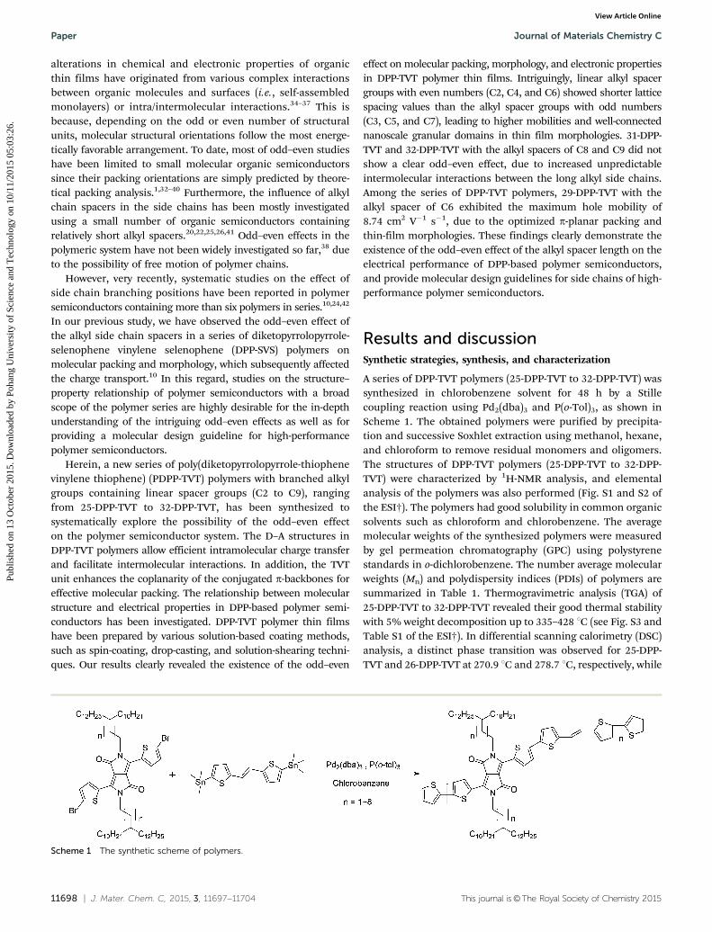
A series of DPP-TVT polymers (25-DPP-TVT to 32-DPP-TVT) wassynthesized in chlorobenzene solvent for 48 h by a Stillecoupling reaction using Pd2(dba)3 and P(o-Tol)3, as shown inScheme 1. The obtained polymers were purified by precipita-tion and successive Soxhlet extraction using methanol, hexane,and chloroform to remove residual monomers and oligomers.The structures of DPP-TVT polymers (25-DPP-TVT to 32-DPP-TVT) were characterized by 1H-NMR analysis, and elementalanalysis of the polymers was also performed (Fig. S1 and S2 ofthe ESI†). The polymers had good solubility in common organicsolvents such as chloroform and chlorobenzene. The averagemolecular weights of the synthesized polymers were measuredby gel permeation chromatography (GPC) using polystyrenestandards in o-dichlorobenzene. The number average molecularweights (Mn) and polydispersity indices (PDIs) of polymers aresummarized in Table 1. Thermogravimetric analysis (TGA) of25-DPP-TVT to 32-DPP-TVT revealed their good thermal stabilitywith 5% weight decomposition up to 335–428 1C (see Fig. S3 andTable S1 of the ESI†). In differential scanning calorimetry (DSC)analysis, a distinct phase transition was observed for 25-DPP-TVT and 26-DPP-TVT at 270.9 1C and 278.7 1C, respectively, while
Scheme 1 The synthetic scheme of polymers.
Paper Journal of Materials Chemistry C
Publ
ishe
d on
13
Oct
ober
201
5. D
ownl
oade
d by
Poh
ang
Uni
vers
ity o
f Sc
ienc
e an
d T
echn
olog
y on
10/
11/2
015
05:0
3:26
. View Article Online

This journal is©The Royal Society of Chemistry 2015 J. Mater. Chem. C, 2015, 3, 11697--11704 | 11699
no phase transition was observed from 50 to 300 1C for 27-DPP-TVT to 32-DPP-TVT (see Fig. S4 and Table S1 of the ESI†).
The UV-vis absorption spectra of the DPP-TVT polymer series(25-DPP-TVT to 32-DPP-TVT) in chloroform solution and thinfilm are displayed in Fig. 1, with the data being summarized inTable 1. The polymers exhibit dual optical absorption from300 to 1000 nm with small high- and intense low-energy bandsattributed to the localized p–p* and internal charge transfer(ICT) transitions, respectively. The absorption maxima ofpolymer films showed slightly wider and broader absorptionscompared with those of solution (Fig. 1). The solution spectrashowed slightly red shifted absorption by approximately 10–12 nmwhen going from 25-DPP-TVT to 32-DPP-TVT, which may resultfrom the reduced steric hindrance by introducing a larger linearspace group between the branching point and the backbone.Interestingly, the solution and thin film spectra showed distinctdual-bands of 0–1 transition and 0–0 transition, which dependedon the odd–even characteristic of the number of linear spacegroups. This indicates that the close packing of the rigid andplanar backbone is closely related to the odd–even characteristic ofthe number of linear space groups. The highest occupied molecularorbital (HOMO) energy levels of all the polymers were measured bycyclic voltammetry, and the resulting HOMO values were between
�5.25 eV and �5.28 eV with optical band gaps from 1.23 eV to1.37 eV (Table 1 and Fig. S5 of the ESI†).
Microstructural analysis of polymer films
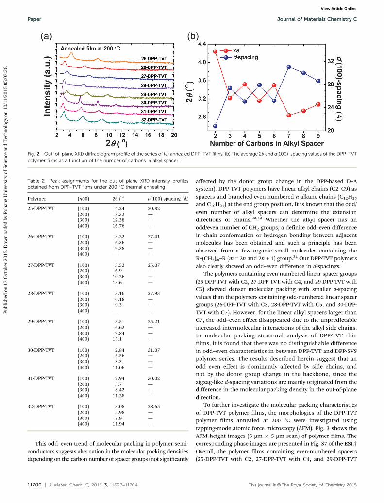
The molecular packing and crystallinity of the DPP-TVT polymerseries (25-DPP-TVT to 32-DPP-TVT) in the film state were investi-gated by performing out-of-plane X-ray diffraction (XRD) analysis.In the annealed polymer films (200 1C for 10 min), well-definedstrong (n00) reflection peaks were observed with higher-orderdiffraction peaks up to (400) reflections, while the as-cast DPP-TVT films exhibited relatively weak and broad diffraction peaks(Fig. S6 and Table S2 of the ESI†). Interestingly, a series of DPP-TVT polymer films containing the spacer group from C2 to C7(from 25-DPP-TVT to 30-DPP-TVT) exhibited broadly fluctuating(100) diffraction peaks as shown in Fig. 2a. Such an odd–eveneffect was clearly observed in the average 2y and d-spacing valuesof the DPP-TVT polymer films (Fig. 2b) and the correspondingout-of-plane XRD data are summarized in Table 2. These resultsshowed that the even-numbered linear spacer groups (25-DPP-TVT with C2, 27-DPP-TVT with C4, and 29-DPP-TVT with C6) hadshorter d-spacing values than those of the polymers with odd-numbered linear spacer groups (26-DPP-TVT with C3, 28-DPP-TVTwith C5, and 30-DPP-TVT with C7).
Table 1 Summary of the optical and electrochemical properties, and the number average molecular weight (Mn) and polydispersity of polymersdetermined by using GPC with polystyrene as the standard
Polymerl0–0
max Sola
[nm]l0–1
max Sola
[nm]l0–0
max filmb
[nm]l0–1
max filmb
[nm]Band gap(optical) [eV]
LUMO(optical) [eV]
HOMO(electrochemical)c [eV]
Mnd
[kDa] (PDI)
25-DPP-TVT 776 ne 785 721 1.31 �3.97 �5.28 633 (1.27)26-DPP-TVT 784 n 802 n 1.23 �4.03 �5.26 348 (3.28)27-DPP-TVT 779 742 781 728 1.29 �3.98 �5.27 284 (2.25)28-DPP-TVT 778 n 778 726 1.37 �3.90 �5.27 49 (5.90)29-DPP-TVT 799 745 800 734 1.28 �3.97 �5.25 519 (2.67)30-DPP-TVT 795 n 795 n 1.27 �4.00 �5.27 44 (1.26)31-DPP-TVT 786 n 787 727 1.32 �3.94 �5.26 179 (3.22)32-DPP-TVT 791 743 791 736 1.30 �3.97 �5.27 242 (2.39)
a UV-absorption for solution was measured by using a chloroform solution of 10�4 M. b UV-absorption for film was measured by spin coating using0.2 wt% solution. c CV was measured in a solution containing Bu4NClO4 (0.1 M) in acetonitrile. d GPC was measured by polystyrene standard inchlorobenzene solvent. e Not observed.
Fig. 1 UV-vis-NIR absorption of the series of DPP-TVT polymers in (a) chloroform solution and (b) thin films.
Journal of Materials Chemistry C Paper
Publ
ishe
d on
13
Oct
ober
201
5. D
ownl
oade
d by
Poh
ang
Uni
vers
ity o
f Sc
ienc
e an
d T
echn
olog
y on
10/
11/2
015
05:0
3:26
. View Article Online
11700 | J. Mater. Chem. C, 2015, 3, 11697--11704 This journal is©The Royal Society of Chemistry 2015
This odd–even trend of molecular packing in polymer semi-conductors suggests alternation in the molecular packing densitiesdepending on the carbon number of spacer groups (not significantly
affected by the donor group change in the DPP-based D–Asystem). DPP-TVT polymers have linear alkyl chains (C2–C9) asspacers and branched even-numbered n-alkane chains (C12H25
and C10H21) at the end group position. It is known that the odd/even number of alkyl spacers can determine the extensiondirections of chains.32,43 Whether the alkyl spacer has anodd/even number of CH2 groups, a definite odd–even differencein chain conformation or hydrogen bonding between adjacentmolecules has been obtained and such a principle has beenobserved from a few organic small molecules containing theR–(CH2)m–R (m = 2n and 2n + 1) group.32 Our DPP-TVT polymersalso clearly showed an odd–even difference in d-spacings.
The polymers containing even-numbered linear spacer groups(25-DPP-TVT with C2, 27-DPP-TVT with C4, and 29-DPP-TVT withC6) showed denser molecular packing with smaller d-spacingvalues than the polymers containing odd-numbered linear spacergroups (26-DPP-TVT with C3, 28-DPP-TVT with C5, and 30-DPP-TVT with C7). However, for the linear alkyl spacers larger thanC7, the odd–even effect disappeared due to the unpredictableincreased intermolecular interactions of the alkyl side chains.In molecular packing structural analysis of DPP-TVT thinfilms, it is found that there was no distinguishable differencein odd–even characteristics in between DPP-TVT and DPP-SVSpolymer series. The results described herein suggest that anodd–even effect is dominantly affected by side chains, andnot by the donor group change in the backbone, since thezigzag-like d-spacing variations are mainly originated from thedifference in the molecular packing density in the out-of-planedirection.
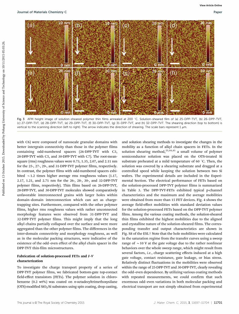
To further investigate the molecular packing characteristicsof DPP-TVT polymer films, the morphologies of the DPP-TVTpolymer films annealed at 200 1C were investigated usingtapping-mode atomic force microscopy (AFM). Fig. 3 shows theAFM height images (5 mm � 5 mm scan) of polymer films. Thecorresponding phase images are presented in Fig. S7 of the ESI.†Overall, the polymer films containing even-numbered spacers(25-DPP-TVT with C2, 27-DPP-TVT with C4, and 29-DPP-TVT
Fig. 2 Out-of-plane XRD diffractogram profile of the series of (a) annealed DPP-TVT films. (b) The average 2y and d(100)-spacing values of the DPP-TVTpolymer films as a function of the number of carbons in alkyl spacer.
Table 2 Peak assignments for the out-of-plane XRD intensity profilesobtained from DPP-TVT films under 200 1C thermal annealing
Polymer (n00) 2y (1) d(100)-spacing (Å)
25-DPP-TVT (100) 4.24 20.82(200) 8.32 —(300) 12.38 —(400) 16.76 —
26-DPP-TVT (100) 3.22 27.41(200) 6.36 —(300) 9.38 —(400) — —
27-DPP-TVT (100) 3.52 25.07(200) 6.9 —(300) 10.26 —(400) 13.6 —
28-DPP-TVT (100) 3.16 27.93(200) 6.18 —(300) 9.3 —(400) — —
29-DPP-TVT (100) 3.5 25.21(200) 6.62 —(300) 9.84 —(400) 13.1 —
30-DPP-TVT (100) 2.84 31.07(200) 5.56 —(300) 8.3 —(400) 11.06 —
31-DPP-TVT (100) 2.94 30.02(200) 5.7 —(300) 8.42 —(400) 11.28 —
32-DPP-TVT (100) 3.08 28.65(200) 5.98 —(300) 8.9 —(400) 11.94 —
Paper Journal of Materials Chemistry C
Publ
ishe
d on
13
Oct
ober
201
5. D
ownl
oade
d by
Poh
ang
Uni
vers
ity o
f Sc
ienc
e an
d T
echn
olog
y on
10/
11/2
015
05:0
3:26
. View Article Online
This journal is©The Royal Society of Chemistry 2015 J. Mater. Chem. C, 2015, 3, 11697--11704 | 11701
with C6) were composed of nanoscale granular domains withbetter intergrain connectivity than those in the polymer filmscontaining odd-numbered spacers (26-DPP-TVT with C3,28-DPP-TVT with C5, and 30-DPP-TVT with C7). The root-mean-square (rms) roughness values were 0.73, 1.35, 2.07, and 2.11 nmfor the 25-, 27-, 29-, and 31-DPP-TVT polymer films, respectively.In contrast, the polymer films with odd-numbered spacers exhi-bited B1.2 times higher average rms roughness values (1.17,2.17, 1.21, and 2.71 nm for the 26-, 28-, 30-, and 32-DPP-TVTpolymer films, respectively). Thin films based on 26-DPP-TVT,28-DPP-TVT, and 30-DPP-TVT molecules showed comparativelyunfavorable interconnected grains with larger holes withindomain–domain interconnection which can act as charge-trapping sites. Furthermore, compared with the other polymerfilms, higher rms roughness values with rather unconnectedmorphology features were observed from 31-DPP-TVT and32-DPP-TVT polymer films. This might imply that the longalkyl chains partially collapsed over the surface and were moreaggregated than the other polymer films. The differences in theinter-domain connectivity and morphology roughness, as wellas in the molecular packing structures, were indicative of theexistence of the odd–even effect of the alkyl chain spacer in theDPP-TVT thin-film microstructures.
Fabrication of solution-processed FETs and I–Vcharacterization
To investigate the charge transport property of a series ofDPP-TVT polymer films, we fabricated bottom-gate top-contactfield-effect transistors (FETs). The polymer solution in chloro-benzene (0.2 wt%) was coated on n-octadecyltrimethoxysilane(OTS)-modified SiO2/Si substrates using spin coating, drop casting,
and solution shearing methods to investigate the changes in themobility as a function of alkyl chain spacers in FETs. In thesolution shearing method,25,44,45 a small volume of polymersemiconductor solution was placed on the OTS-treated Sisubstrate preheated at a mild temperature of 60 1C. Then, thesolution was covered by a shearing substrate and dragged at acontrolled speed while keeping the solution between two Siwafers. The experimental details are included in the Experi-mental Section. The electrical performance of FETs based onthe solution-processed DPP-TVT polymer films is summarizedin Table 3. The DPP-TVT-FETs exhibited typical p-channelcharacteristics and the maximum and the average mobilitieswere obtained from more than 15 FET devices. Fig. 4 shows theaverage field-effect mobilities with standard deviation valuesfor the solution-processed FETs based on the DPP-TVT polymerfilms. Among the various coating methods, the solution-shearedthin films exhibited the highest mobilities due to the alignedand crystalline nature of the solution-sheared films. The corres-ponding transfer and output characteristics are shown inFig. S8 of the ESI.† Note that the hole mobilities were calculatedin the saturation regime from the transfer curves using a sweeprange of B10 V at the gate voltage due to the rather nonlinearbehaviors over the whole sweep range, which might result fromseveral factors, i.e., charge scattering effects induced at a highgate voltage, contact resistance, gate leakage, or bias stress.Relatively distinct fluctuations in the mobilities were observedwithin the range of 25-DPP-TVT and 30-DPP-TVT, clearly revealingthe odd–even dependence. By utilizing various coating methodswith repeated measurements, we could confirm that suchenormous odd–even variations in both molecular packing andelectrical transport are not simply obtained from experimental
Fig. 3 AFM height image of solution-sheared polymer thin films annealed at 200 1C. Solution-sheared film of (a) 25-DPP-TVT, (b) 26-DPP-TVT,(c) 27-DPP-TVT, (d) 28-DPP-TVT, (e) 29-DPP-TVT, (f) 30-DPP-TVT, (g) 31-DPP-TVT, and (h) 32-DPP-TVT. The shearing direction (top to bottom) isvertical to the scanning direction (left to right). The arrow indicates the direction of shearing. The scale bars represent 1 mm.
Journal of Materials Chemistry C Paper
Publ
ishe
d on
13
Oct
ober
201
5. D
ownl
oade
d by
Poh
ang
Uni
vers
ity o
f Sc
ienc
e an
d T
echn
olog
y on
10/
11/2
015
05:0
3:26
. View Article Online

11702 | J. Mater. Chem. C, 2015, 3, 11697--11704 This journal is©The Royal Society of Chemistry 2015
fluctuations in error ranges. In addition to the observation ofthe odd–even effect in the hole transport, the optimized sidechain-containing molecule was found to be 29-DPP-TVT with a
C6 spacer unit. The solution-sheared 29-DPP-TVT films showedthe highest average hole mobility of 8.29 � 0.46 cm2 V�1 s�1,with the maximum mobility of 8.74 cm2 V�1 s�1 at VGS, VDS =� 100 V, due to their shorter d-spacing value and well-interconnected nanoscale granular domains observed in theAFM morphology image.
To explore the practical applications of the optimized29-DPP-TVT, photo-responses of 29-DPP-TVT FETs were inves-tigated upon on-and-off switching of polychromatic light(l = 450–650 nm, lmax = 640 nm, and Pmax = 36 mW cm�2) inthe transistor off-state (VGS = 0 V and VDS = � 100 V) (Fig. S9 ofthe ESI†). The photogenerated charge carriers produced notice-able photocurrents in 29-DPP-TVT FETs. Their highly reprodu-cible photosensitivity could substantiate the potential of29-DPP-TVT for use in photo-sensing applications. In addition,30-DPP-TVT FETs exhibited much lower performance in contrastto 30-DPP-SVS FETs (the average hole mobility of 30-DPP-TVTwas 1.09 � 0.08 cm2 V�1 s�1, while that of 30-DPP-SVS FETs was9.78 � 1.64 cm2 V�1 s�1 in our previous report10). This mightresult from the much larger d-spacing value of 30-DPP-TVT thinfilm than that of 30-DPP-SVS, leading to unfavorable chargetransport in OFET performance (the d-spacing of 30-DPP-TVTwas 31.07 Å, while the d-spacing of 30-DPP-SVS was 28.0 Å). Onthe other hand, slight variations in the mobility were observed byincreasing the side chain length (number) above 30-DPP-TVT.Such variation in the odd–even effect was consistent with theresults from XRD and AFM analyses.
ExperimentalAFM characterization
An Agilent 5500 (Agilent, USA) scanning probe microscope(SPM) equipped with a Nanoscope V controller was used toobtain AFM images of DPP-TVT thin films. AFM images wererecorded in high-resolution tapping mode under ambientconditions.
FET fabrication and testing
FET devices with bottom-gate top-contact configuration wereprepared to characterize the electrical performance of a series ofDPP-TVT polymers. A highly n-doped (100) Si wafer (o0.004 O cm)with a thermally grown SiO2 (300 nm, Ci = 10 nF cm�2) was utilizedas the substrate and dielectric. The surface of SiO2 was modifiedwith the n-octadecyltrimethoxysilane (OTS) self-assembled mono-layer (SAM) as previously reported.37,46,47 3 mM of OTS solution intrichloroethylene was spin-coated on the piranha-cleaned wafer at3000 rpm for 30 s. Then, the wafer was exposed to ammonia vaporfor B12 h to facilitate the formation of OTS SAM, followed bysonication cleaning, sequential washing, and drying. The contactangle on the hydrophobic OTS-modified wafer with D.I. waterdroplets was 41061. The DPP-TVT polymers were dissolved inchlorobenzene (0.2 wt%) and the film was prepared on thesubstrate by various solution-processing methods; spin-coating,drop-casting, and solution-shearing.44,45 In solution-shearing,the substrate temperature and shearing speed were optimized
Table 3 FET performance of DPP-TVT thin films
Conditionsa p-Channel
Polymer Filmsmh,max
b
[cm2 V�1 s�1]mh,avg
c
[cm2 V�1 s�1] Ion/Ioff
25-DPP-TVT Spin-coated 2.62 1.98 (�0.27)d 4104
Drop-cast 3.59 3.38 (�0.20) 4105
Solution-sheared 4.10 3.91 (�0.61) 4106
26-DPP-TVT Spin-coated 0.63 0.57 (�0.03) 4104
Drop-cast 0.71 0.65 (�0.03) 4105
Solution-sheared 0.80 0.71 (�0.08) 4107
27-DPP-TVT Spin-coated 2.81 1.41 (�0.23) 4103
Drop-cast 4.35 3.11 (�0.57) 4106
Solution-sheared 4.69 4.10 (�0.46) 4106
28-DPP-TVT Spin-coated 0.23 0.20 (�0.01) 4106
Drop-cast 0.26 0.23 (�0.01) 4105
Solution-sheared 1.20 0.96 (�0.13) 4105
29-DPP-TVT Spin-coated 5.24 3.21 (�0.87) 4106
Drop-cast 5.76 4.08 (�0.68) 4107
Solution-sheared 8.74 8.29 (�0.46) 4106
30-DPP-TVT Spin-coated 0.77 0.57 (�0.14) 4105
Drop-cast 0.90 0.71 (�0.12) 4105
Solution-sheared 1.23 1.09 (�0.08) 4105
31-DPP-TVT Spin-coated 3.60 3.18 (�0.10) 4105
Drop-cast 4.37 4.17 (�0.15) 4106
Solution-sheared 6.69 6.08 (�0.39) 4107
32-DPP-TVT Spin-coated 3.27 3.10 (�0.11) 4106
Drop-cast 4.31 3.64 (�0.66) 4106
Solution-sheared 4.85 4.09 (�0.44) 4105
a The p-channel characteristics of DPP-TVT FETs were measured at VDS =�100 V. b The maximum mobility over 15 FET devices with a channellength (L) of B50 mm and a channel width (W) of B1000 mm. c Theaverage mobility over 15 FET devices with a channel length (L) of B50 mmand a channel width (W) of B1000 mm. d The standard deviation.
Fig. 4 The average field-effect mobilities obtained from the annealedDPP-TVT thin-film transistors. The distinct odd–even trend with the sidechain length is observed in the range of 25-DPP-TVT to 32-DPP-TVT.
Paper Journal of Materials Chemistry C
Publ
ishe
d on
13
Oct
ober
201
5. D
ownl
oade
d by
Poh
ang
Uni
vers
ity o
f Sc
ienc
e an
d T
echn
olog
y on
10/
11/2
015
05:0
3:26
. View Article Online

This journal is©The Royal Society of Chemistry 2015 J. Mater. Chem. C, 2015, 3, 11697--11704 | 11703
to 60 1C and 0.12 mm s�1, respectively for thin film formation(thickness o30 nm). Then, the polymer thin-film was annealedon a hot plate at 200 1C for 10 min under a N2 atmosphere. Goldcontacts (40 nm) were thermally evaporated onto the polymerfilm to form source and drain electrodes with a channel length(L) of B50 mm and a channel width (W) of B1000 mm using ashadow mask. The electrical performance of FETs was measuredin a N2-filled glove box using a Keithley 4200 semiconductorparametric analyzer. The field-effect mobility was calculated inthe saturation regime using the following equation:
ID ¼W
2LmCi VGS � VTð Þ2
where ID is the drain-to-source current, W and L are the semi-conductor channel width and length, respectively, m is themobility, and VGS and VT are the gate voltage and thresholdvoltage, respectively.
Conclusion
A series of DPP-TVT polymers ranging from 25-DPP-TVT to32-DPP-TVT, with branched alkyl groups containing linearspacer groups from C2 to C9, was synthesized to systematicallyinvestigate the structure–property relationship, especially tostudy the odd–even effect induced by the number of carbonatoms in the alkyl spacer of the DPP-TVT polymer side chains.The solid-state molecular packing density and charge transportcapability were clearly altered, depending on whether the numberwas odd or even. Linear alkyl spacer groups with even numbersof carbon atoms (C2, C4, and C6) exhibited shorter latticespacings than did spacer groups with odd numbers of carbonatoms (C3, C5, and C7), resulting in higher hole mobilities.The optimal alkyl spacer length was confirmed by a series ofDPP-TVT polymers and 29-DPP-TVT containing the C6 linearspacer group exhibited the maximum hole mobility of8.74 cm2 V�1 s�1 (VGS and VDS = �100 V). Our findingssystematically confirm the existence of odd–even effects as afunction of alkyl spacer length in the side chain of DPP-basedpolymer semiconductors. The optimized side chain geometrywith the alkyl spacer of C6 effectively facilitated charge trans-port via the synergistic effect of optimized molecular packingand film morphology. Our results provide practical guidelinesfor the side chain engineering to develop high-performancepolymer semiconductors.
Acknowledgements
This work was supported by the Center for Advanced SoftElectronics under the Global Frontier Research Program(2013M3A6A5073175 and 2013M3A6A5073172) of the Ministryof Science, ICT and Future Planning, and by the NationalResearch Foundation of Korea (2014R1A2A2A01007467 and2012R1A2A2A06047047). H.Y. acknowledges financial supportfrom the Global PhD Fellowship.
References
1 J. Mei, Y. Diao, A. L. Appleton, L. Fang and Z. Bao, J. Am.Chem. Soc., 2013, 135, 6724–6746.
2 H. Sirringhaus, Adv. Mater., 2014, 26, 1319–1335.3 H. Dong, X. Fu, J. Liu, Z. Wang and W. Hu, Adv. Mater.,
2013, 25, 6158–6183.4 T. L. Nelson, T. M. Young, J. Y. Liu, S. P. Mishra, J. A. Belot,
C. L. Balliet, A. E. Javier, T. Kowalewski and R. D.McCullough, Adv. Mater., 2010, 22, 4617–4621.
5 S. C. Ng, H. S. O. Chan, T. T. Ong, K. Kumura, Y. Mazaki andK. Kobayashi, Macromolecules, 1998, 31, 1221–1228.
6 Y. Zhao, Y. Guo and Y. Liu, Adv. Mater., 2013, 25, 5372–5391.7 W. Y. Lee, G. Giri, Y. Diao, C. J. Tassone, J. R. Matthews,
M. L. Sorensen, S. C. B. Mannsfeld, W. C. Chen, H. H. Fong,J. B. H. Tok, M. F. Toney, M. Q. He and Z. Bao, Adv. Funct.Mater., 2014, 24, 3524–3534.
8 H.-J. Yun, H. H. Choi, S.-K. Kwon, Y.-H. Kim and K. Cho,Chem. Mater., 2014, 26, 3928–3937.
9 H.-R. Tseng, H. Phan, C. Luo, M. Wang, L. A. Perez,S. N. Patel, L. Ying, E. J. Kramer, T.-Q. Nguyen, G. C.Bazan and A. J. Heeger, Adv. Mater., 2014, 26, 2993–2998.
10 J. Y. Back, H. Yu, I. Song, I. Kang, H. Ahn, T. J. Shin, S.-K.Kwon, J. H. Oh and Y.-H. Kim, Chem. Mater., 2015, 27,1732–1739.
11 J. Li, Y. Zhao, H. S. Tan, Y. Guo, C. A. Di, G. Yu, Y. Liu,M. Lin, S. H. Lim, Y. Zhou, H. Su and B. S. Ong, Sci. Rep.,2012, 2, 754.
12 I. Kang, H. J. Yun, D. S. Chung, S. K. Kwon and Y. H. Kim,J. Am. Chem. Soc., 2013, 135, 14896–14899.
13 A. R. Han, G. K. Dutta, J. Lee, H. R. Lee, S. M. Lee, H. Ahn,T. J. Shin, J. H. Oh and C. Yang, Adv. Funct. Mater., 2015, 25,247–254.
14 K. Takimiya, I. Osaka and M. Nakano, Chem. Mater., 2014,26, 587–593.
15 W. Jiang, Y. Li and Z. H. Wang, Chem. Soc. Rev., 2013, 42,6113–6127.
16 W. P. Wu, Y. Q. Liu and D. B. Zhu, Chem. Soc. Rev., 2010, 39,1489–1502.
17 Z. Chen, M. J. Lee, R. Shahid Ashraf, Y. Gu, S. Albert-Seifried, M. Meedom Nielsen, B. Schroeder, T. D.Anthopoulos, M. Heeney, I. McCulloch and H. Sirringhaus,Adv. Mater., 2012, 24, 647–652.
18 J. D. Yuen, J. Fan, J. Seifter, B. Lim, R. Hufschmid, A. J.Heeger and F. Wudl, J. Am. Chem. Soc., 2011, 133,20799–20807.
19 T. Lei, Y. Cao, Y. L. Fan, C. J. Liu, S. C. Yuan and J. Pei, J. Am.Chem. Soc., 2011, 133, 6099–6101.
20 T. Lei, J. H. Dou and J. Pei, Adv. Mater., 2012, 24, 6457–6461.21 B. Fu, J. Baltazar, A. R. Sankar, P.-H. Chu, S. Zhang,
D. M. Collard and E. Reichmanis, Adv. Funct. Mater., 2014,24, 3734–3744.
22 I. Meager, R. S. Ashraf, S. Mollinger, B. C. Schroeder,H. Bronstein, D. Beatrup, M. S. Vezie, T. Kirchartz, A. Salleo,J. Nelson and I. McCulloch, J. Am. Chem. Soc., 2013, 135,11537–11540.
Journal of Materials Chemistry C Paper
Publ
ishe
d on
13
Oct
ober
201
5. D
ownl
oade
d by
Poh
ang
Uni
vers
ity o
f Sc
ienc
e an
d T
echn
olog
y on
10/
11/2
015
05:0
3:26
. View Article Online
11704 | J. Mater. Chem. C, 2015, 3, 11697--11704 This journal is©The Royal Society of Chemistry 2015
23 F. J. Zhang, Y. B. Hu, T. Schuettfort, C. A. Di, X. K. Gao,C. R. McNeill, L. Thomsen, S. C. B. Mannsfeld, W. Yuan,H. Sirringhaus and D. B. Zhu, J. Am. Chem. Soc., 2013, 135,2338–2349.
24 J.-H. Dou, Y.-Q. Zheng, T. Lei, S.-D. Zhang, Z. Wang, W.-B.Zhang, J.-Y. Wang and J. Pei, Adv. Funct. Mater., 2014, 24,6270–6278.
25 J. Lee, A. R. Han, H. Yu, T. J. Shin, C. Yang and J. H. Oh,J. Am. Chem. Soc., 2013, 135, 9540–9547.
26 J. Lee, A. R. Han, J. Kim, Y. Kim, J. H. Oh and C. Yang, J. Am.Chem. Soc., 2012, 134, 20713–20721.
27 H. J. Chen, Y. L. Guo, G. Yu, Y. Zhao, J. Zhang, D. Gao, H. T.Liu and Y. Q. Liu, Adv. Mater., 2012, 24, 4618–4622.
28 J. Mei, D. H. Kim, A. L. Ayzner, M. F. Toney and Z. Bao, J. Am.Chem. Soc., 2011, 133, 20130–20133.
29 K. R. Graham, C. Cabanetos, J. P. Jahnke, M. N. Idso, A. ElLabban, G. O. Ngongang Ndjawa, T. Heumueller, K. Vandewal,A. Salleo, B. F. Chmelka, A. Amassian, P. M. Beaujuge andM. D. McGehee, J. Am. Chem. Soc., 2014, 136, 9608–9618.
30 T. Lei, J. Y. Wang and J. Pei, Chem. Mater., 2014, 26, 594–603.31 J. Mei and Z. Bao, Chem. Mater., 2014, 26, 604–615.32 F. Tao and S. L. Bernasek, Chem. Rev., 2007, 107, 1408–1453.33 H. B. Akkerman, S. C. B. Mannsfeld, A. P. Kaushik,
E. Verploegen, L. Burnier, A. P. Zoombelt, J. D. Saathoff,S. Hong, S. Atahan-Evrenk, X. L. Liu, A. Aspuru-Guzik,M. F. Toney, P. Clancy and Z. Bao, J. Am. Chem. Soc., 2013,135, 11006–11014.
34 J. H. Oh, W. Y. Lee, T. Noe, W. C. Chen, M. Konemann andZ. Bao, J. Am. Chem. Soc., 2011, 133, 4204–4207.
35 K. H. Kim, H. Yu, H. Kang, D. J. Kang, C. H. Cho, H. H.Cho, J. H. Oh and B. J. Kim, J. Mater. Chem. A, 2013, 1,14538–14547.
36 M. Gsanger, J. H. Oh, M. Konemann, H. W. Hoffken,A. M. Krause, Z. Bao and F. Wurthner, Angew. Chem., Int.Ed., 2010, 49, 740–743.
37 R. Schmidt, J. H. Oh, Y. S. Sun, M. Deppisch, A. M. Krause,K. Radacki, H. Braunschweig, M. Konemann, P. Erk,Z. Bao and F. Wurthner, J. Am. Chem. Soc., 2009, 131,6215–6228.
38 R. Marty, R. Nigon, D. Leite and H. Frauenrath, J. Am. Chem.Soc., 2014, 136, 3919–3927.
39 H. Ebata, T. Izawa, E. Miyazaki, K. Takimiya, M. Ikeda,H. Kuwabara and T. Yui, J. Am. Chem. Soc., 2007, 129,15732–15733.
40 X.-Y. Wang, F.-D. Zhuang, X. Zhou, D.-C. Yang, J.-Y. Wangand J. Pei, J. Mater. Chem. C, 2014, 2, 8152–8161.
41 S. Chen, B. Sun, W. Hong, H. Aziz, Y. Meng and Y. Li,J. Mater. Chem. C, 2014, 2, 2183–2190.
42 J. Mei, H.-C. Wu, Y. Diao, A. Appleton, H. Wang, Y. Zhou,W.-Y. Lee, T. Kurosawa, W.-C. Chen and Z. Bao, Adv. Funct.Mater., 2015, 25, 3455–3462.
43 T. Toledano, H. Sazan, S. Mukhopadhyay, H. Alon, K. Lerman,T. Bendikov, D. T. Major, C. N. Sukenik, A. Vilan andD. Cahen, Langmuir, 2014, 30, 13596–13605.
44 G. Giri, E. Verploegen, S. C. Mannsfeld, S. Atahan-Evrenk,H. Kim do, S. Y. Lee, H. A. Becerril, A. Aspuru-Guzik, M. F.Toney and Z. Bao, Nature, 2011, 480, 504–508.
45 H. A. Becerril, M. E. Roberts, Z. H. Liu, J. Locklin and Z. Bao,Adv. Mater., 2008, 20, 2588–2594.
46 Y. Ito, A. A. Virkar, S. Mannsfeld, J. H. Oh, M. Toney, J. Locklinand Z. Bao, J. Am. Chem. Soc., 2009, 131, 9396–9404.
47 A. Virkar, S. Mannsfeld, J. H. Oh, M. F. Toney, Y. H. Tan,G. Y. Liu, J. C. Scott, R. Miller and Z. Bao, Adv. Funct. Mater.,2009, 19, 1962–1970.
Paper Journal of Materials Chemistry C
Publ
ishe
d on
13
Oct
ober
201
5. D
ownl
oade
d by
Poh
ang
Uni
vers
ity o
f Sc
ienc
e an
d T
echn
olog
y on
10/
11/2
015
05:0
3:26
. View Article Online